JP2016508286A - Solar cell conductive contact seed layer - Google Patents
Solar cell conductive contact seed layer Download PDFInfo
- Publication number
- JP2016508286A JP2016508286A JP2015546559A JP2015546559A JP2016508286A JP 2016508286 A JP2016508286 A JP 2016508286A JP 2015546559 A JP2015546559 A JP 2015546559A JP 2015546559 A JP2015546559 A JP 2015546559A JP 2016508286 A JP2016508286 A JP 2016508286A
- Authority
- JP
- Japan
- Prior art keywords
- solar cell
- conductive layer
- substrate
- particles
- contact
- Prior art date
- Legal status (The legal status is an assumption and is not a legal conclusion. Google has not performed a legal analysis and makes no representation as to the accuracy of the status listed.)
- Granted
Links
- 229910052710 silicon Inorganic materials 0.000 claims abstract description 110
- 239000000758 substrate Substances 0.000 claims abstract description 106
- 239000010703 silicon Substances 0.000 claims abstract description 82
- XUIMIQQOPSSXEZ-UHFFFAOYSA-N Silicon Chemical compound [Si] XUIMIQQOPSSXEZ-UHFFFAOYSA-N 0.000 claims abstract description 81
- 239000000203 mixture Substances 0.000 claims abstract description 43
- 239000002245 particle Substances 0.000 claims abstract description 38
- 229910052782 aluminium Inorganic materials 0.000 claims abstract description 36
- XAGFODPZIPBFFR-UHFFFAOYSA-N aluminium Chemical compound [Al] XAGFODPZIPBFFR-UHFFFAOYSA-N 0.000 claims abstract description 36
- 238000009792 diffusion process Methods 0.000 claims abstract description 19
- PXHVJJICTQNCMI-UHFFFAOYSA-N Nickel Chemical compound [Ni] PXHVJJICTQNCMI-UHFFFAOYSA-N 0.000 claims description 38
- 239000011856 silicon-based particle Substances 0.000 claims description 38
- 229910021420 polycrystalline silicon Inorganic materials 0.000 claims description 36
- 238000000137 annealing Methods 0.000 claims description 14
- 239000011230 binding agent Substances 0.000 claims description 14
- 230000015572 biosynthetic process Effects 0.000 claims description 14
- 239000010949 copper Substances 0.000 claims description 14
- 229910021419 crystalline silicon Inorganic materials 0.000 claims description 8
- RYGMFSIKBFXOCR-UHFFFAOYSA-N Copper Chemical compound [Cu] RYGMFSIKBFXOCR-UHFFFAOYSA-N 0.000 claims description 7
- 229910052802 copper Inorganic materials 0.000 claims description 7
- 229910052759 nickel Inorganic materials 0.000 claims description 7
- XLOMVQKBTHCTTD-UHFFFAOYSA-N Zinc monoxide Chemical compound [Zn]=O XLOMVQKBTHCTTD-UHFFFAOYSA-N 0.000 claims description 6
- 239000011521 glass Substances 0.000 claims description 6
- XOLBLPGZBRYERU-UHFFFAOYSA-N tin dioxide Chemical compound O=[Sn]=O XOLBLPGZBRYERU-UHFFFAOYSA-N 0.000 claims description 6
- 229910001887 tin oxide Inorganic materials 0.000 claims description 6
- 230000005641 tunneling Effects 0.000 claims description 4
- 238000000034 method Methods 0.000 abstract description 20
- 229920005591 polysilicon Polymers 0.000 description 23
- 238000010304 firing Methods 0.000 description 10
- 238000005424 photoluminescence Methods 0.000 description 10
- 238000004519 manufacturing process Methods 0.000 description 7
- 239000002904 solvent Substances 0.000 description 6
- 239000000463 material Substances 0.000 description 5
- 238000007639 printing Methods 0.000 description 5
- 230000015556 catabolic process Effects 0.000 description 3
- 238000006731 degradation reaction Methods 0.000 description 3
- 230000005496 eutectics Effects 0.000 description 3
- 238000010587 phase diagram Methods 0.000 description 3
- 239000004065 semiconductor Substances 0.000 description 3
- 229910018125 Al-Si Inorganic materials 0.000 description 2
- 229910018520 Al—Si Inorganic materials 0.000 description 2
- VYPSYNLAJGMNEJ-UHFFFAOYSA-N Silicium dioxide Chemical compound O=[Si]=O VYPSYNLAJGMNEJ-UHFFFAOYSA-N 0.000 description 2
- 239000000654 additive Substances 0.000 description 2
- 230000000996 additive effect Effects 0.000 description 2
- CSDREXVUYHZDNP-UHFFFAOYSA-N alumanylidynesilicon Chemical compound [Al].[Si] CSDREXVUYHZDNP-UHFFFAOYSA-N 0.000 description 2
- 239000006117 anti-reflective coating Substances 0.000 description 2
- 238000013459 approach Methods 0.000 description 2
- 239000002019 doping agent Substances 0.000 description 2
- 238000007772 electroless plating Methods 0.000 description 2
- 230000005855 radiation Effects 0.000 description 2
- 238000001878 scanning electron micrograph Methods 0.000 description 2
- 229910018098 Ni-Si Inorganic materials 0.000 description 1
- 229910005883 NiSi Inorganic materials 0.000 description 1
- 229910018529 Ni—Si Inorganic materials 0.000 description 1
- 229910000676 Si alloy Inorganic materials 0.000 description 1
- BQCADISMDOOEFD-UHFFFAOYSA-N Silver Chemical compound [Ag] BQCADISMDOOEFD-UHFFFAOYSA-N 0.000 description 1
- 229910045601 alloy Inorganic materials 0.000 description 1
- 239000000956 alloy Substances 0.000 description 1
- 238000001354 calcination Methods 0.000 description 1
- 229910017052 cobalt Inorganic materials 0.000 description 1
- 239000010941 cobalt Substances 0.000 description 1
- GUTLYIVDDKVIGB-UHFFFAOYSA-N cobalt atom Chemical compound [Co] GUTLYIVDDKVIGB-UHFFFAOYSA-N 0.000 description 1
- 239000013078 crystal Substances 0.000 description 1
- 230000008021 deposition Effects 0.000 description 1
- 238000004090 dissolution Methods 0.000 description 1
- 238000009713 electroplating Methods 0.000 description 1
- 238000010438 heat treatment Methods 0.000 description 1
- 238000007641 inkjet printing Methods 0.000 description 1
- 238000000608 laser ablation Methods 0.000 description 1
- 238000001459 lithography Methods 0.000 description 1
- 229910052751 metal Inorganic materials 0.000 description 1
- 239000002184 metal Substances 0.000 description 1
- 229910021421 monocrystalline silicon Inorganic materials 0.000 description 1
- 238000000059 patterning Methods 0.000 description 1
- 229920001296 polysiloxane Polymers 0.000 description 1
- 238000010248 power generation Methods 0.000 description 1
- 238000005215 recombination Methods 0.000 description 1
- 230000006798 recombination Effects 0.000 description 1
- 238000007788 roughening Methods 0.000 description 1
- 238000007650 screen-printing Methods 0.000 description 1
- 239000000377 silicon dioxide Substances 0.000 description 1
- 235000012239 silicon dioxide Nutrition 0.000 description 1
- 229910052709 silver Inorganic materials 0.000 description 1
- 239000004332 silver Substances 0.000 description 1
- WFKWXMTUELFFGS-UHFFFAOYSA-N tungsten Chemical compound [W] WFKWXMTUELFFGS-UHFFFAOYSA-N 0.000 description 1
- 229910052721 tungsten Inorganic materials 0.000 description 1
- 239000010937 tungsten Substances 0.000 description 1
Images


Classifications
-
- H—ELECTRICITY
- H01—ELECTRIC ELEMENTS
- H01L—SEMICONDUCTOR DEVICES NOT COVERED BY CLASS H10
- H01L31/00—Semiconductor devices sensitive to infrared radiation, light, electromagnetic radiation of shorter wavelength or corpuscular radiation and specially adapted either for the conversion of the energy of such radiation into electrical energy or for the control of electrical energy by such radiation; Processes or apparatus specially adapted for the manufacture or treatment thereof or of parts thereof; Details thereof
- H01L31/02—Details
- H01L31/0224—Electrodes
- H01L31/022408—Electrodes for devices characterised by at least one potential jump barrier or surface barrier
- H01L31/022425—Electrodes for devices characterised by at least one potential jump barrier or surface barrier for solar cells
- H01L31/022441—Electrode arrangements specially adapted for back-contact solar cells
-
- H—ELECTRICITY
- H01—ELECTRIC ELEMENTS
- H01B—CABLES; CONDUCTORS; INSULATORS; SELECTION OF MATERIALS FOR THEIR CONDUCTIVE, INSULATING OR DIELECTRIC PROPERTIES
- H01B1/00—Conductors or conductive bodies characterised by the conductive materials; Selection of materials as conductors
- H01B1/04—Conductors or conductive bodies characterised by the conductive materials; Selection of materials as conductors mainly consisting of carbon-silicon compounds, carbon or silicon
-
- H—ELECTRICITY
- H01—ELECTRIC ELEMENTS
- H01B—CABLES; CONDUCTORS; INSULATORS; SELECTION OF MATERIALS FOR THEIR CONDUCTIVE, INSULATING OR DIELECTRIC PROPERTIES
- H01B1/00—Conductors or conductive bodies characterised by the conductive materials; Selection of materials as conductors
- H01B1/20—Conductive material dispersed in non-conductive organic material
- H01B1/24—Conductive material dispersed in non-conductive organic material the conductive material comprising carbon-silicon compounds, carbon or silicon
-
- H—ELECTRICITY
- H01—ELECTRIC ELEMENTS
- H01L—SEMICONDUCTOR DEVICES NOT COVERED BY CLASS H10
- H01L31/00—Semiconductor devices sensitive to infrared radiation, light, electromagnetic radiation of shorter wavelength or corpuscular radiation and specially adapted either for the conversion of the energy of such radiation into electrical energy or for the control of electrical energy by such radiation; Processes or apparatus specially adapted for the manufacture or treatment thereof or of parts thereof; Details thereof
- H01L31/04—Semiconductor devices sensitive to infrared radiation, light, electromagnetic radiation of shorter wavelength or corpuscular radiation and specially adapted either for the conversion of the energy of such radiation into electrical energy or for the control of electrical energy by such radiation; Processes or apparatus specially adapted for the manufacture or treatment thereof or of parts thereof; Details thereof adapted as photovoltaic [PV] conversion devices
- H01L31/06—Semiconductor devices sensitive to infrared radiation, light, electromagnetic radiation of shorter wavelength or corpuscular radiation and specially adapted either for the conversion of the energy of such radiation into electrical energy or for the control of electrical energy by such radiation; Processes or apparatus specially adapted for the manufacture or treatment thereof or of parts thereof; Details thereof adapted as photovoltaic [PV] conversion devices characterised by at least one potential-jump barrier or surface barrier
- H01L31/068—Semiconductor devices sensitive to infrared radiation, light, electromagnetic radiation of shorter wavelength or corpuscular radiation and specially adapted either for the conversion of the energy of such radiation into electrical energy or for the control of electrical energy by such radiation; Processes or apparatus specially adapted for the manufacture or treatment thereof or of parts thereof; Details thereof adapted as photovoltaic [PV] conversion devices characterised by at least one potential-jump barrier or surface barrier the potential barriers being only of the PN homojunction type, e.g. bulk silicon PN homojunction solar cells or thin film polycrystalline silicon PN homojunction solar cells
- H01L31/0682—Semiconductor devices sensitive to infrared radiation, light, electromagnetic radiation of shorter wavelength or corpuscular radiation and specially adapted either for the conversion of the energy of such radiation into electrical energy or for the control of electrical energy by such radiation; Processes or apparatus specially adapted for the manufacture or treatment thereof or of parts thereof; Details thereof adapted as photovoltaic [PV] conversion devices characterised by at least one potential-jump barrier or surface barrier the potential barriers being only of the PN homojunction type, e.g. bulk silicon PN homojunction solar cells or thin film polycrystalline silicon PN homojunction solar cells back-junction, i.e. rearside emitter, solar cells, e.g. interdigitated base-emitter regions back-junction cells
-
- H—ELECTRICITY
- H01—ELECTRIC ELEMENTS
- H01L—SEMICONDUCTOR DEVICES NOT COVERED BY CLASS H10
- H01L31/00—Semiconductor devices sensitive to infrared radiation, light, electromagnetic radiation of shorter wavelength or corpuscular radiation and specially adapted either for the conversion of the energy of such radiation into electrical energy or for the control of electrical energy by such radiation; Processes or apparatus specially adapted for the manufacture or treatment thereof or of parts thereof; Details thereof
- H01L31/04—Semiconductor devices sensitive to infrared radiation, light, electromagnetic radiation of shorter wavelength or corpuscular radiation and specially adapted either for the conversion of the energy of such radiation into electrical energy or for the control of electrical energy by such radiation; Processes or apparatus specially adapted for the manufacture or treatment thereof or of parts thereof; Details thereof adapted as photovoltaic [PV] conversion devices
- H01L31/06—Semiconductor devices sensitive to infrared radiation, light, electromagnetic radiation of shorter wavelength or corpuscular radiation and specially adapted either for the conversion of the energy of such radiation into electrical energy or for the control of electrical energy by such radiation; Processes or apparatus specially adapted for the manufacture or treatment thereof or of parts thereof; Details thereof adapted as photovoltaic [PV] conversion devices characterised by at least one potential-jump barrier or surface barrier
- H01L31/072—Semiconductor devices sensitive to infrared radiation, light, electromagnetic radiation of shorter wavelength or corpuscular radiation and specially adapted either for the conversion of the energy of such radiation into electrical energy or for the control of electrical energy by such radiation; Processes or apparatus specially adapted for the manufacture or treatment thereof or of parts thereof; Details thereof adapted as photovoltaic [PV] conversion devices characterised by at least one potential-jump barrier or surface barrier the potential barriers being only of the PN heterojunction type
- H01L31/0745—Semiconductor devices sensitive to infrared radiation, light, electromagnetic radiation of shorter wavelength or corpuscular radiation and specially adapted either for the conversion of the energy of such radiation into electrical energy or for the control of electrical energy by such radiation; Processes or apparatus specially adapted for the manufacture or treatment thereof or of parts thereof; Details thereof adapted as photovoltaic [PV] conversion devices characterised by at least one potential-jump barrier or surface barrier the potential barriers being only of the PN heterojunction type comprising a AIVBIV heterojunction, e.g. Si/Ge, SiGe/Si or Si/SiC solar cells
- H01L31/0747—Semiconductor devices sensitive to infrared radiation, light, electromagnetic radiation of shorter wavelength or corpuscular radiation and specially adapted either for the conversion of the energy of such radiation into electrical energy or for the control of electrical energy by such radiation; Processes or apparatus specially adapted for the manufacture or treatment thereof or of parts thereof; Details thereof adapted as photovoltaic [PV] conversion devices characterised by at least one potential-jump barrier or surface barrier the potential barriers being only of the PN heterojunction type comprising a AIVBIV heterojunction, e.g. Si/Ge, SiGe/Si or Si/SiC solar cells comprising a heterojunction of crystalline and amorphous materials, e.g. heterojunction with intrinsic thin layer or HIT® solar cells; solar cells
-
- Y—GENERAL TAGGING OF NEW TECHNOLOGICAL DEVELOPMENTS; GENERAL TAGGING OF CROSS-SECTIONAL TECHNOLOGIES SPANNING OVER SEVERAL SECTIONS OF THE IPC; TECHNICAL SUBJECTS COVERED BY FORMER USPC CROSS-REFERENCE ART COLLECTIONS [XRACs] AND DIGESTS
- Y02—TECHNOLOGIES OR APPLICATIONS FOR MITIGATION OR ADAPTATION AGAINST CLIMATE CHANGE
- Y02E—REDUCTION OF GREENHOUSE GAS [GHG] EMISSIONS, RELATED TO ENERGY GENERATION, TRANSMISSION OR DISTRIBUTION
- Y02E10/00—Energy generation through renewable energy sources
- Y02E10/50—Photovoltaic [PV] energy
- Y02E10/546—Polycrystalline silicon PV cells
-
- Y—GENERAL TAGGING OF NEW TECHNOLOGICAL DEVELOPMENTS; GENERAL TAGGING OF CROSS-SECTIONAL TECHNOLOGIES SPANNING OVER SEVERAL SECTIONS OF THE IPC; TECHNICAL SUBJECTS COVERED BY FORMER USPC CROSS-REFERENCE ART COLLECTIONS [XRACs] AND DIGESTS
- Y02—TECHNOLOGIES OR APPLICATIONS FOR MITIGATION OR ADAPTATION AGAINST CLIMATE CHANGE
- Y02E—REDUCTION OF GREENHOUSE GAS [GHG] EMISSIONS, RELATED TO ENERGY GENERATION, TRANSMISSION OR DISTRIBUTION
- Y02E10/00—Energy generation through renewable energy sources
- Y02E10/50—Photovoltaic [PV] energy
- Y02E10/547—Monocrystalline silicon PV cells
Abstract
太陽電池導電性コンタクトのシード層、及び太陽電池導電性コンタクトのシード層の形成方法が開示される。例えば、太陽電池は基板を含む。基板上にエミッタ領域が配置される。導電性コンタクトはエミッタ領域上に配置され、エミッタ領域と接触する導電層を含む。導電層は、およそ15%超のSiとその残りのAl、という組成を有する、複数のアルミニウム/シリコン(Al/Si)粒子から成る。別の実施例において、太陽電池は、基板の表面、又はその付近に拡散領域を有する基板を含む。導電性コンタクトは拡散領域の上方に配置され、基板と接触する導電層を含む。導電層は、およそ15%超のSiとその残りのAl、という組成を有する、複数のアルミニウム/シリコン(Al/Si)粒子から成る。A seed layer for a solar cell conductive contact and a method for forming a seed layer for a solar cell conductive contact are disclosed. For example, a solar cell includes a substrate. An emitter region is disposed on the substrate. The conductive contact is disposed on the emitter region and includes a conductive layer in contact with the emitter region. The conductive layer is composed of a plurality of aluminum / silicon (Al / Si) particles having a composition of approximately greater than 15% Si and the remaining Al. In another embodiment, the solar cell includes a substrate having a diffusion region at or near the surface of the substrate. The conductive contact is disposed above the diffusion region and includes a conductive layer that contacts the substrate. The conductive layer is composed of a plurality of aluminum / silicon (Al / Si) particles having a composition of approximately greater than 15% Si and the remaining Al.
Description
本発明の実施形態は、再生可能エネルギーの分野、特に、太陽電池導電性コンタクトのシード層、及び太陽電池導電性コンタクトのシード層の形成方法の分野に属する。 Embodiments of the present invention belong to the field of renewable energy, in particular, the field of solar cell conductive contact seed layers and methods of forming solar cell conductive contact seed layers.
一般的に太陽電池として知られる光電池は、太陽放射を電気エネルギーへと直接変換するための既知の装置である。一般的に、太陽電池は、基板の表面付近にp−n接合を形成する半導体処理技術を使用して、半導体ウエファ又は基板上に製造される。太陽放射が基板の表面に衝突し、基板の中に入ると、基板のバルク内に電子及び正孔の対が生成する。電子及び正孔の対が基板のpドープ及びnドープ領域に移動することにより、ドープ領域間における電圧差が生じる。ドープ領域は、太陽電池の導電性領域に接続され、電流を太陽電池からそれと連結された外部回路へと方向付ける。 Photovoltaic cells, commonly known as solar cells, are known devices for directly converting solar radiation into electrical energy. In general, solar cells are fabricated on a semiconductor wafer or substrate using semiconductor processing techniques that form a pn junction near the surface of the substrate. When solar radiation strikes the surface of the substrate and enters the substrate, electron and hole pairs are generated in the bulk of the substrate. As the electron and hole pairs move to the p-doped and n-doped regions of the substrate, a voltage difference occurs between the doped regions. The doped region is connected to the conductive region of the solar cell and directs current from the solar cell to an external circuit coupled thereto.
効率は、太陽電池の発電能力に直接関係するので、太陽電池の重要な特性である。同様に、太陽電池を生産する上での効率は、このような太陽電池の費用効果に直接関係する。したがって、太陽電池の効率を向上させるための技術、又は太陽電池の製造における効率を向上させるための技術が、一般的に望ましい。本発明の幾つかの実施形態は、太陽電池構造体を製造するための新規なプロセスを提供することによって、太陽電池の製造効率の向上を可能にする。本発明の幾つかの実施形態は、新規な太陽電池構造体を提供することによって、太陽電池の効率向上を可能にしている。 Efficiency is an important characteristic of a solar cell because it is directly related to the power generation capacity of the solar cell. Similarly, the efficiency in producing solar cells is directly related to the cost effectiveness of such solar cells. Therefore, a technique for improving the efficiency of a solar cell or a technique for improving the efficiency in manufacturing a solar cell is generally desirable. Some embodiments of the present invention allow for improved solar cell manufacturing efficiency by providing a novel process for manufacturing solar cell structures. Some embodiments of the present invention allow for improved solar cell efficiency by providing a novel solar cell structure.
太陽電池導電性コンタクトのシード層、及び太陽電池導電性コンタクトのシード層の形成方法が本明細書において記載される。以下の記載において、本発明の実施形態の完全な理解をもたらすために、具体的なプロセスフロー作業など、多くの具体的詳細が説明される。本発明の実施形態が、これらの具体的な詳細に捕われずに実施され得ることが、当業者には明らかとなる。他の場合には、本発明の実施形態を不必要に不明瞭にしないために、リソグラフィ及びパターニング技術などの、周知の製造技術は詳細に説明されない。更に、図中に示される様々な実施形態は例示的な表現であり、必ずしも縮尺通りに描かれていないことが理解される。 A seed layer for a solar cell conductive contact and a method for forming a seed layer for a solar cell conductive contact are described herein. In the following description, numerous specific details are set forth, such as specific process flow operations, in order to provide a thorough understanding of embodiments of the present invention. It will be apparent to those skilled in the art that embodiments of the present invention may be practiced without these specific details. In other instances, well-known manufacturing techniques, such as lithography and patterning techniques, will not be described in detail so as not to unnecessarily obscure the embodiments of the present invention. Further, it is understood that the various embodiments shown in the figures are exemplary representations and are not necessarily drawn to scale.
複数の導電性コンタクトを有する太陽電池が本明細書において開示される。一実施形態において、太陽電池は基板を含む。基板上にエミッタ領域が配置される。導電性コンタクトはエミッタ領域上に配置され、エミッタ領域と接触する導電層を含む。導電層は、およそ15%超のSiとその残りのAl、という組成を有する、複数のアルミニウム/シリコン(Al/Si)粒子から成る。別の実施形態において、太陽電池は、基板の表面、又は表面の付近に、拡散領域を有する基板を含む。導電性コンタクトは拡散領域の上方に配置され、基板と接触する導電層を含む。導電層は、およそ15%超のSiとその残りのAl、という組成を有する、複数のアルミニウム/シリコン(Al/Si)粒子から成る。更に他の(別の)実施形態において、部分的に製造された太陽電池が基板を含む。エミッタ領域は、基板内、又は基板の上方に配置される。導電性コンタクトは、エミッタ領域のシリコン領域上に配置され、シリコン領域と接触する導電層を含む。導電層は、導電層のアニール中に導電層がシリコン領域の有意な部分を消耗することがないように、十分な量のSiを備える組成を有する、複数のアルミニウム/シリコン(Al/Si)粒子から成る。組成の残りの部分はAlである。 Disclosed herein is a solar cell having a plurality of conductive contacts. In one embodiment, the solar cell includes a substrate. An emitter region is disposed on the substrate. The conductive contact is disposed on the emitter region and includes a conductive layer in contact with the emitter region. The conductive layer is composed of a plurality of aluminum / silicon (Al / Si) particles having a composition of approximately greater than 15% Si and the remaining Al. In another embodiment, the solar cell includes a substrate having a diffusion region at or near the surface of the substrate. The conductive contact is disposed above the diffusion region and includes a conductive layer that contacts the substrate. The conductive layer is composed of a plurality of aluminum / silicon (Al / Si) particles having a composition of approximately greater than 15% Si and the remaining Al. In yet another (another) embodiment, a partially fabricated solar cell includes a substrate. The emitter region is disposed in the substrate or above the substrate. The conductive contact is disposed on the silicon region of the emitter region and includes a conductive layer in contact with the silicon region. The conductive layer has a plurality of aluminum / silicon (Al / Si) particles having a composition with a sufficient amount of Si so that the conductive layer does not consume a significant portion of the silicon region during annealing of the conductive layer. Consists of. The rest of the composition is Al.
本明細書において記載される1つ以上の実施形態は、複数の印刷される導電性シード粒子内にシリコンを含めることにより、シリコンベースのエミッタ領域内のフォトルミネッセンス(PL)の劣化を制御することを対象としている。より具体的に、最初に形成される導電性印刷シード層から、導電性コンタクトを形成するときに、複数のアルミニウム−シリコン合金粒子から成るペーストが印刷され得る。ペーストは、装置に電気コンタクトを形成するため(及び、例えば、溶媒を熱してペーストから除去するため)に焼成又はアニールされる。装置基板、又は他のシリコン層のシリコンは、焼成中、アルミニウムに急速に溶解し得る。基板からのシリコンが溶解すると、これにより基板中に複数のピットが生じる場合がある。これらのピットはひいては、装置の表面において高度な再結合を生じる場合があり、PL信号の減少、及び装置の効率性の低減を生じる。1つ以上の実施形態において、このように基板からのシリコンの溶解を防ぐために、ペースト自体の中に十分なシリコンも含むようにして、アルミニウムが堆積される。 One or more embodiments described herein control photoluminescence (PL) degradation in a silicon-based emitter region by including silicon in a plurality of printed conductive seed particles. Is targeted. More specifically, a paste consisting of a plurality of aluminum-silicon alloy particles can be printed from the initially formed conductive printing seed layer when forming the conductive contacts. The paste is fired or annealed to make electrical contacts to the device (and to remove the solvent from the paste by, for example, heating). The device substrate, or other silicon layer silicon, can rapidly dissolve in aluminum during firing. As the silicon from the substrate dissolves, this may cause multiple pits in the substrate. These pits can in turn cause a high degree of recombination at the surface of the device, resulting in a decrease in the PL signal and a reduction in the efficiency of the device. In one or more embodiments, aluminum is deposited such that it also includes sufficient silicon in the paste itself to prevent dissolution of the silicon from the substrate.
シリコンによるピットの形成は、堆積されるアルミニウム膜にいくらかのシリコンを含める(例えば、約1%のシリコンが有効であり得る)ことにより、軽減又は排除することができる。追加のシリコンが高温においてアルミニウムに溶解することにより、基板から溶解するシリコンが殆ど又は全くなくなる。一実施例において、我々独自の試験が、およそ550℃で焼成したスパッタリングしたアルミニウム膜において、ピット形成を防ぐのにおよそ2%のシリコンしか必要とされないことを示した。更に、577℃という、アルミニウム−シリコン共晶を超える焼成温度において、必要とされるシリコンの量は位相図に従うものと予測される。しかしながら、およそ5マイクロメートルの直径であり、およそ580℃で焼成された複数のアルミニウムの粒子から作製されたアルミニウム膜で発明者らが行った試験では、12%のシリコンが含まれている場合にピット形成が生じた。Al/Si共晶の位相図に基づけば、12%のシリコンが含まれていれば、ピット形成を低減し、PLを改善するのに十分なはずであった。実際には、使用される複数の粒子内のシリコンが15%未満であると、PLの劣化を防ぐためには不十分であることが見出された。したがって、アルミニウム/シリコン共晶点、又はこれを超える温度でアルミニウムペーストを焼成するためには、一実施形態において、位相図により元来示されるものよりも多くのシリコンがペーストに含まれる。しかしながら、一実施形態において、ペーストが効果的な導電性ペーストでなくならないためには、限られた量のシリコンのみが含まれ得る。一実施例として、図1は、本発明の実施形態による、ペースト状添加物内の標的シリコン(Si)含有量の関数としての、フォトルミネッセンス(PL)中央点(焼成後)のプロット100である。プロット100において看取されるように、PLの劣化と、シリコン含有量との間には関係性がある。
The formation of pits by silicon can be reduced or eliminated by including some silicon in the deposited aluminum film (eg, about 1% silicon can be effective). As additional silicon dissolves in aluminum at high temperatures, little or no silicon dissolves from the substrate. In one example, our own test showed that in a sputtered aluminum film fired at approximately 550 ° C., only approximately 2% silicon is required to prevent pit formation. Furthermore, at a calcination temperature of 577 ° C., which exceeds the aluminum-silicon eutectic, the amount of silicon required is expected to follow a phase diagram. However, tests conducted by the inventors on aluminum films that were approximately 5 micrometers in diameter and made from a plurality of aluminum particles fired at approximately 580 ° C. showed that they contained 12% silicon. Pit formation occurred. Based on the Al / Si eutectic phase diagram, 12% silicon should have been sufficient to reduce pit formation and improve PL. In practice, it has been found that less than 15% silicon in the particles used is insufficient to prevent PL degradation. Thus, to fire the aluminum paste at or above the aluminum / silicon eutectic point, in one embodiment, the paste contains more silicon than originally shown by the phase diagram. However, in one embodiment, only a limited amount of silicon can be included so that the paste must not be an effective conductive paste. As an example, FIG. 1 is a
一実施形態において、アルミニウムベースの導電性シードペーストにおいて、アルミニウムに対して15%超のシリコンが含まれる。1つのこのような実施形態において、25%ものシリコンが使用される。25%近い使用量は、その上にペーストが堆積されたシリコン領域におけるピット形成を低減することができる。例えば、本発明の実施形態により、図2Aは、内部のアルミニウムに対して15%のシリコンを有するシードペーストを焼成した後のシリコン基板の走査型電子顕徽鏡(SEM)画像200Aであり、一方で、図2Bは、内部のアルミニウムに対して25%のシリコンを有するシードペーストの焼成後のシリコン基板のSEM画像200Bである。画像200A及び200Bの比較において看取され得るように、25%の相対シリコン量に対し、15%の相対シリコン量においてより多くのピット形成が生じた。 In one embodiment, the aluminum-based conductive seed paste includes greater than 15% silicon relative to aluminum. In one such embodiment, as much as 25% silicon is used. A usage of close to 25% can reduce pit formation in the silicon area on which the paste is deposited. For example, in accordance with an embodiment of the present invention, FIG. 2A is a scanning electron microscope (SEM) image 200A of a silicon substrate after firing a seed paste having 15% silicon relative to the internal aluminum, FIG. 2B is an SEM image 200B of the silicon substrate after firing the seed paste having 25% silicon with respect to the inner aluminum. As can be seen in the comparison of images 200A and 200B, more pit formation occurred at 15% relative silicon content versus 25% relative silicon content.
第1の態様において、複数のAl/Si粒子を有するシード層は、太陽電池の基板の上方に形成される複数のエミッタ領域を有する太陽電池のための、複数の裏面コンタクトなどの複数のコンタクトを製造するために、使用され得る。例えば、本発明の実施形態により、図3Aは、基板の上方に形成される複数のエミッタ領域上に形成される複数の導電性コンタクトを有する太陽電池の一部の断面図を例示する。 In a first aspect, a seed layer having a plurality of Al / Si particles comprises a plurality of contacts, such as a plurality of back contacts, for a solar cell having a plurality of emitter regions formed above a substrate of the solar cell. Can be used to manufacture. For example, according to an embodiment of the invention, FIG. 3A illustrates a cross-sectional view of a portion of a solar cell having a plurality of conductive contacts formed on a plurality of emitter regions formed above the substrate.
図3Aを参照し、太陽電池300Aの一部は、複数のn型ドープポリシリコン領域420、複数のp型ドープポリシリコン領域422、及び複数のトレンチ416により露出される基板400のオン部分の上方に配置されたパターン付き誘電層424を含む。複数の導電性コンタクト428は、誘電層424内に配置された複数のコンタクト開口部内に配置され、複数のn型ドープポリシリコン領域420、及び複数のp型ドープポリシリコン領域422に連結される。パターン付き誘電層、複数のn型ドープポリシリコン領域420、複数のp型ドープのポリシリコン領域422、基板400、及び複数のトレンチ416の材料、及び製造方法は、図4A〜4Cに関連して以下に記載され得る。更に、複数のn型ドープポリシリコン領域420、及び複数のp型ドープポリシリコン領域422は、一実施形態において、太陽電池300Aのエミッタ領域をもたらし得る。このように、一実施形態において、複数の導電性コンタクト428は、複数のエミッタ領域上に配置される。一実施形態において、複数の導電性コンタクト428は、バックコンタクト型太陽電池のための複数のバックコンタクトであり、太陽電池300Aの受光表面(図3Aに401として示される方向)と反対側の太陽電池表面上に位置する。更に、一実施形態において、複数のエミッタ領域は、薄い又はトンネル誘電層402(図4Aと関連して更に詳細に記載される)上に形成される。
Referring to FIG. 3A, a portion of
一実施形態において、図3Aを再び参照し、複数の導電性コンタクト428のそれぞれは、太陽電池300Aの複数のエミッタ領域と接触する、導電層330を含む。1つのこのような実施形態において、導電層330は、複数のアルミニウム/シリコン(Al/Si)粒子から成り、複数の粒子は、およそ15%超のSiと、残りの部分のAlという組成を有する。特定のこのような実施形態において、複数のAl/Si粒子はおよそ25%未満のSiと、残りの部分のAlという組成を有する。一実施形態において、複数のAl/Si粒子は微結晶性である。1つのこのような実施形態において、複数のAl/Si粒子の結晶性は、およそ550〜580℃の範囲の温度で行われるアニール(例えば、レーザー焼成が挙げられるがこれに限定されない)により生じる。しかしながら、別の実施形態において、複数のAl/Si粒子は相分離している。
In one embodiment, referring again to FIG. 3A, each of the plurality of
一実施形態において、導電層330は、およそ10〜30%の結合剤及びフリットと、残りの部分の複数のAl/Si粒子を含む、全組成物を有する。1つのこのような実施形態において、結合剤は、酸化亜鉛(ZnO)、酸化スズ(SnO)、又は両方から成り、フリットは複数のガラス粒子から成る。最初に適用されるとき、シード層(例えば、適用される際の層330)は更に、溶媒を含む。しかしながら、上記のように、シード層をアニールして、溶媒が除去され、最終的な構成において、本質的に結合剤、フリット、及び複数のAl/Si粒子が残される。
In one embodiment, the
一実施形態において、導電層330は、およそ100マイクロメートルよりも大きな厚さを有し、そこから製造される導電性コンタクト428は、本質的に導電層330のみからなる太陽電池のバックコンタクトである。しかしながら、別の実施形態において、導電層330は、およそ2〜10マイクロメートルの厚さを有する。この実施形態において、図3Aに示されるように、導電性コンタクト428は、太陽電池のバックコンタクトであり、導電層330、導電層330上に配置された無電解めっきニッケル(Ni)層332、及びNi層上に配置された電気めっき銅(Cu)層334から成る。
In one embodiment,
第2の態様において、複数のAl/Si粒子を有するシード層は、太陽電池の基板内に形成された複数のエミッタ領域を有する太陽電池のための、複数の裏面コンタクトなどの複数のコンタクトを製造するために使用され得る。例えば図3Bは、本発明の実施形態による、基板内に形成された複数のエミッタ領域上に形成された複数の導電性コンタクトを有する太陽電池の一部の断面図を例示する。 In a second aspect, a seed layer having a plurality of Al / Si particles produces a plurality of contacts, such as a plurality of back contacts, for a solar cell having a plurality of emitter regions formed in a substrate of the solar cell. Can be used to For example, FIG. 3B illustrates a cross-sectional view of a portion of a solar cell having a plurality of conductive contacts formed on a plurality of emitter regions formed in a substrate, according to an embodiment of the invention.
図3Bを参照し、太陽電池300Bの一部は、複数のn型ドープ拡散領域320、複数のp型ドープ拡散領域322、及びバルク結晶シリコン基板などの基板300のオン部分の上方に配置されたパターン付き誘電層324を含む。複数の導電性コンタクト328は、誘電層324内に配置される複数のコンタクト開口部内に配置され、複数のn型ドープ拡散領域320、及び複数のp型ドープ拡散領域322に連結されている。一実施形態において、拡散領域320及び322は、複数のn型ドーパント及び複数のp型ドーパントをそれぞれ備えるシリコン基板の複数のドープ領域により形成される。更に、複数のn型ドープ拡散領域320、及び複数のp型ドープ拡散領域322は一実施形態において、太陽電池300Bの複数のエミッタ領域をもたらす。一実施形態において、複数の導電性コンタクト328は、複数のエミッタ領域上に配置される。一実施形態において、図3Bに示されるように、導電性コンタクト328は、バックコンタクト型太陽電池のバックコンタクトであり、反対側の粗面化受光表面301など、受光表面と反対側の太陽電池の表面上に位置する。
Referring to FIG. 3B, a portion of solar cell 300B is disposed above an ON portion of
一実施形態において、図3Bを再び参照し、複数の導電性コンタクト328のそれぞれは、太陽電池300Bの複数のエミッタ領域と接触する、導電層330を含む。1つのこのような実施形態において、導電層330は、複数のアルミニウム/シリコン(Al/Si)粒子から成り、複数の粒子は、およそ15%超のSiと、残りの部分のAlという組成を有する。特定のこのような実施形態において、複数のAl/Si粒子はおよそ25%未満のSiと、残りの部分のAlという組成を有する。一実施形態において、複数のAl/Si粒子は微結晶性である。1つのこのような実施形態において、複数のAl/Si粒子の結晶性は、およそ550〜580℃の範囲の温度で行われるアニール(例えば、レーザー焼成が挙げられるがこれに限定されない)により生じる。しかしながら、別の実施形態において、複数のAl/Si粒子は相分離している。
In one embodiment, referring again to FIG. 3B, each of the plurality of conductive contacts 328 includes a
一実施形態において、導電層330は、およそ10〜30%の結合剤及びフリットと、残りの部分の複数のAl/Si粒子を含む、全組成物を有する。1つのこのような実施形態において、結合剤は、酸化亜鉛(ZnO)、酸化スズ(SnO)、又は両方から成り、フリットは複数のガラス粒子から成る。最初に適用されるとき、シード層(例えば、適用される際の層330)は更に、溶媒を含む。しかしながら、上記のように、シード層をアニールして、溶媒が除去され、最終的な構成において、本質的に結合剤、フリット、及び複数のAl/Si粒子が残される。
In one embodiment, the
一実施形態において、導電層330は、およそ100マイクロメートルよりも大きな厚さを有し、そこから製造される複数の導電性コンタクト328は、本質的に導電層330のみからなる太陽電池のバックコンタクトである。しかしながら、別の実施形態において、導電層330は、およそ2〜10マイクロメートルの厚さを有する。この実施形態において、図3Bに示されるように、導電性コンタクト328は、太陽電池のバックコンタクトであり、導電層330、導電層330上に配置された無電解めっきニッケル(Ni)層332、及びNi層上に配置された電気めっき銅(Cu)層334から成る。
In one embodiment, the
図1及び図2Bを再び参照し、かつ図3A及び3Bに関連して、一実施形態において、部分的に製造された太陽電池は、基板、基板内又はその上方に配置されるエミッタ領域、及びエミッタ領域のシリコン領域上に配置された(例えば、ポリシリコン層、又はシリコン基板上に配置された)導電性コンタクトを含む。1つのこのような実施形態において、導電性コンタクトは、シリコン領域と接触している導電層を含む。導電層は、導電層が導電層のアニール(例えば、レーザー焼成)中に、シリコン領域の有意な部分を消耗させることがないように、十分な量のSiを含む組成を有する、複数のアルミニウム/シリコン(Al/Si)粒子から成る。特定の実施形態において、Al/Si組成物の残りの部分はAlである。ある実施形態において、複数のAl/Si粒子は、およそ15%超、およそ25%未満のSiと、残りの部分のAlを備える組成を有する。 Referring back to FIGS. 1 and 2B and in conjunction with FIGS. 3A and 3B, in one embodiment, a partially fabricated solar cell includes a substrate, an emitter region disposed in or above the substrate, and A conductive contact is disposed on the silicon region of the emitter region (eg, disposed on a polysilicon layer or a silicon substrate). In one such embodiment, the conductive contact includes a conductive layer in contact with the silicon region. The conductive layer includes a plurality of aluminum / silicone compositions having a sufficient amount of Si so that the conductive layer does not consume a significant portion of the silicon region during annealing (eg, laser firing) of the conductive layer. It consists of silicon (Al / Si) particles. In certain embodiments, the remaining portion of the Al / Si composition is Al. In some embodiments, the plurality of Al / Si particles have a composition comprising greater than approximately 15%, less than approximately 25% Si, and the remaining Al.
導電層が、アニール中にシリコン領域の有意な部分を消耗することがないように、十分な量のSiを備える組成を有する複数のアルミニウム/シリコン(Al/Si)粒子から成る導電層の使用は、シリコン基板、又は基板の上方に形成されるポリシリコン層から形成されるエミッタ領域を有する構造に使用され得る。例えば、第1実施形態において、参照として図3Aを参照し、太陽電池は、基板上に配置されたトンネリング誘電層上に配置された多結晶シリコン領域から成るエミッタ領域を含む。導電層は、エミッタ領域の上方に配置された絶縁層のトレンチ内に配置され、多結晶シリコン領域と接触している。1つのこのような実施形態において、導電層が多結晶シリコン領域と接触する、多結晶シリコン領域にピット形成が殆ど又は全く存在しない。別の例において、第2実施形態において、参照として図3Bを参照し、太陽電池はバルク結晶シリコン基板から製造され、導電層は、基板表面の上方に配置された絶縁層のトレンチ内に配置される。1つのこのような実施形態において、導電層がバルク結晶シリコン基板と接触するバルク結晶シリコン基板にピット形成が殆ど又は全く存在しない。 The use of a conductive layer composed of a plurality of aluminum / silicon (Al / Si) particles having a composition with a sufficient amount of Si so that the conductive layer does not consume a significant portion of the silicon region during annealing. , A silicon substrate, or a structure having an emitter region formed from a polysilicon layer formed over the substrate. For example, in the first embodiment, referring to FIG. 3A as a reference, a solar cell includes an emitter region consisting of a polycrystalline silicon region disposed on a tunneling dielectric layer disposed on a substrate. The conductive layer is disposed in the trench of the insulating layer disposed above the emitter region, and is in contact with the polycrystalline silicon region. In one such embodiment, there is little or no pit formation in the polycrystalline silicon region where the conductive layer is in contact with the polycrystalline silicon region. In another example, in the second embodiment, referring to FIG. 3B as a reference, the solar cell is fabricated from a bulk crystalline silicon substrate, and the conductive layer is disposed in a trench in an insulating layer disposed above the substrate surface. The In one such embodiment, there is little or no pit formation in the bulk crystalline silicon substrate where the conductive layer contacts the bulk crystalline silicon substrate.
いくつかの材料が上記で具体的に記載されているが、いくつかの材料は、他のもので容易に代替することができ、他のこのような実施形態も、依然として本発明の実施形態の趣旨及び範囲の範囲内である。例えば、一実施形態において、III〜V族の材料基板など、異なる材料基板が、シリコン基板の代わりに使用されてもよい。別の実施形態において、複数の銀(Ag)粒子などが、複数のAl粒子の代わりに、又はこれに加えてシードペースト内に使用されてもよい。別の実施形態において、めっきした、又は同様に堆積させたコバルト(Co)、又はタングステン(W)が、上記のメッキしたNiの代わりに、又はこれに加えて使用され得る。 Although some materials are specifically described above, some materials can be easily substituted with others, and other such embodiments are still present in the embodiments of the present invention. Within the spirit and scope. For example, in one embodiment, a different material substrate, such as a III-V material substrate, may be used in place of the silicon substrate. In another embodiment, a plurality of silver (Ag) particles or the like may be used in the seed paste instead of or in addition to the plurality of Al particles. In another embodiment, plated or similarly deposited cobalt (Co) or tungsten (W) may be used in place of or in addition to the plated Ni described above.
更に、形成される複数のコンタクトは、図3Bに記載されたようにバルク基板上に直接形成される必要はない。例えば、一実施形態において、図3Aに記載されたように、上記に記載されるもののような複数の導電性コンタクトが、バルク基板の上方(例えば、裏面に)に形成された半導体領域上に形成される。一実施例として、図4A〜4Cは、本発明の実施形態により、複数の導電性コンタクトを有する太陽電池を作製する方法における様々な処理操作の断面図を例示する。 Further, the contacts that are formed need not be formed directly on the bulk substrate as described in FIG. 3B. For example, in one embodiment, as described in FIG. 3A, a plurality of conductive contacts, such as those described above, are formed on a semiconductor region formed above (eg, on the back surface) of the bulk substrate. Is done. As an example, FIGS. 4A-4C illustrate cross-sectional views of various processing operations in a method of making a solar cell having a plurality of conductive contacts, according to embodiments of the present invention.
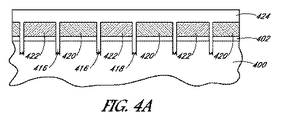
図4Aを参照し、バックコンタクト型太陽電池のコンタクトの形成方法は、基板400上に薄い誘電層402を形成することを含む。
Referring to FIG. 4A, a method for forming a contact of a back contact solar cell includes forming a
一実施形態において、薄い誘電層402は、二酸化ケイ素から成り、およそ5〜50オングストロームの範囲の厚さを有する。一実施形態において、この薄い誘電層402は、トンネリング酸化膜として機能する。一実施形態において、基板400は、n型ドープ単結晶シリコン基板など、バルク単結晶基板である。しかしながら、別の実施形態において、基板400は、太陽電池基板全体の上に配置された多結晶シリコン層を含む。
In one embodiment, the
再び図4Aを参照し、n型ドープポリシリコン領域420と、p型ドープポリシリコン領域422との間にトレンチ416が形成される。また図4Aに示されるように、トレンチ416の一部が、粗面化特徴部418を有するように粗面化されてもよい。
Referring to FIG. 4A again, a
再び図4Aを参照し、誘電層424は、複数のn型ドープポリシリコン領域420、複数のp型ドープポリシリコン領域422、及びトレンチ416により露出した基板400の一部の上方に形成される。一実施形態において、誘電層424の下面は、複数のn型ドープしたポリシリコン領域420、複数のp型ドープポリシリコン領域422、及び基板400の露出部分と共形となるように形成され、一方で誘電層424の上面は、図4Aに示されるように実質的に平坦である。特定の実施形態では、誘電層424は、反射防止膜(ARC)層である。
Referring again to FIG. 4A, a
図4Bを参照し、複数のコンタクト開口部426が、誘電層424内に形成される。複数のコンタクト開口部426は、複数のn型ドープポリシリコン領域420、及び複数のp型ドープポリシリコン領域422への露出をもたらす。一実施形態において、複数のコンタクト開口部426がレーザーアブレーションによって形成される。一実施形態において、図4Bに示されるように、n型ドープポリシリコン領域420に達するコンタクト開口部426は、p型ドープポリシリコン領域422に達するコンタクト開口部と実質的に同じ高さを有する。
Referring to FIG. 4B, a plurality of
図4Cを参照し、バックコンタクト型太陽電池のコンタクトの形成方法は更に、複数のコンタクト開口部426内にあり、複数のn型ドープポリシリコン領域420に連結され、複数のp型ドープポリシリコン領域422に連結された、導電性コンタクト428を形成することを含む。一実施形態において、複数の導電性コンタクト428は、金属から成り、堆積(この堆積は以下でより詳細に記載される)、リソグラフ、及びエッチ手法によって形成される。
Referring to FIG. 4C, the method for forming the contact of the back contact solar cell further includes a plurality of p-type doped polysilicon regions in the plurality of
したがって、一実施形態において、複数の導電性コンタクト428は、バルクN型シリコン基板400の受光表面401と反対側の、バルクN型シリコン基板400の表面上、又は表面の上方に形成される。図4Cに示されるように、特定の実施形態において、複数の導電性コンタクトは、基板400の表面の上方の領域(422/420)上に形成される。形成することには、導電層のアニール中に導電層がシリコン領域の有意な部分を消耗させないように、十分な量のSiを備える組成を有する複数のアルミニウム/シリコン(Al/Si)粒子からなる導電層を形成することを含み得る。特定の実施形態において、Al/Si組成物の残りの部分はAlである。ある実施形態において、複数のAl/Si粒子は、およそ15%超、およそ25%未満のSiと、残りの部分のAlを備える組成を有する。複数の導電性コンタクトを形成することは更に、導電層上に無電解めっきニッケル(Ni)層を形成することを含み得る。加えて、銅(Cu)層は、Ni層上に電気めっきにより形成され得る。
Accordingly, in one embodiment, the plurality of
一実施形態において、導電層を形成することは、バルクN型シリコン基板、又はそのような基板の上方に形成されたポリシリコン層にペーストを印刷することを含む。ペーストは、溶媒、及び複数のアルミニウム/シリコン(Al/Si)合金粒子から成る場合がある。印刷することは、スクリーン印刷、又はインクジェット印刷が挙げられるがこれらに限定されない技術を使用することを含む。加えて、本明細書において記載される1つ以上の実施形態は、無電解めっきNiを内部に組み込むことにより、シリコン基板上に形成された印刷したAlシードの接触抵抗を低減するためのアプローチ、及びそれにより生じる構造を対象としている。より具体的に1つ以上の実施形態が、Alペーストシード層から始まる接触形成を対象としている。ペーストのAlと、その下のシリコン基板との間に接触を形成するために、シード印刷の後にアニールが行われる。次に、Alペーストの上に無電解めっきを行うことにより、Niが堆積される。ペーストは多孔性構造であるため、Niは、複数のAl粒子の上方だけではなく、その外側上にも形成され、少なくとも空隙の一部を満たす。Niは、より多くのNiがAlの上部に形成することができる(Siから離れる)という意味で、等級分けすることができる。それでも、複数のAl粒子の外側の上のNiは、最終的にそこに形成される接触部の接触抵抗を低減するために使用することができる。特に、Alペーストの厚さが全体的に減少すると、Alとシリコンの境界面においてより多くのNiを堆積させることができる。シード印刷の後ではなく、Ni無電解めっきの後にアニールが行われるとき、Ni−Si境界面において、NiSi接触部が形成され得る。更に、複数のAl粒子の空隙、又は孔の中に存在するNiを有することにより、Al−Si境界面にAl−Si接触部が形成され得る。従来の手法と比較して、形成される複数の接触部は、コンタクト構造形成における所与の領域内で、実際の金属のシリコンに対する接触部のより大きな表面積を有し得る。結果として、接触抵抗は、従来のコンタクトと比較してより低くなる場合がある。 In one embodiment, forming the conductive layer includes printing a paste on a bulk N-type silicon substrate, or a polysilicon layer formed over such a substrate. The paste may consist of a solvent and a plurality of aluminum / silicon (Al / Si) alloy particles. Printing includes using techniques that include, but are not limited to, screen printing or ink jet printing. In addition, one or more embodiments described herein include an approach for reducing the contact resistance of printed Al seeds formed on a silicon substrate by incorporating electroless plated Ni therein. And the resulting structure. More specifically, one or more embodiments are directed to contact formation starting from an Al paste seed layer. Annealing is performed after seed printing in order to form a contact between the paste Al and the underlying silicon substrate. Next, Ni is deposited by performing electroless plating on the Al paste. Since the paste has a porous structure, Ni is formed not only above the plurality of Al particles but also on the outside thereof and fills at least part of the voids. Ni can be graded in the sense that more Ni can form on top of Al (away from Si). Nevertheless, the Ni on the outside of the plurality of Al particles can be used to reduce the contact resistance of the contacts that will eventually form there. In particular, when the thickness of the Al paste is reduced as a whole, more Ni can be deposited at the interface between Al and silicon. When annealing is performed after Ni electroless plating rather than after seed printing, NiSi contacts can be formed at the Ni-Si interface. Furthermore, an Al-Si contact portion can be formed at the Al-Si interface by having Ni present in voids or holes of a plurality of Al particles. Compared to conventional approaches, the multiple contacts that are formed may have a larger surface area of the actual metal-to-silicon contact within a given area in the contact structure formation. As a result, the contact resistance may be lower compared to conventional contacts.
したがって、太陽電池導電性コンタクトのシード層、及び太陽電池導電性コンタクトのシード層の形成方法が開示された。本発明の実施形態により、太陽電池は基板を含む。基板上にエミッタ領域が配置される。導電性コンタクトはエミッタ領域上に配置され、エミッタ領域と接触する導電層を含む。導電層は、およそ15%超のSiとその残りのAl、という組成を有する、複数のアルミニウム/シリコン(Al/Si)粒子から成る。一実施形態において、複数のAl/Si粒子は、およそ25%未満のSiと、残りの部分のAlという組成を有する。本発明の別の実施形態により、太陽電池は、基板の表面、又は表面の付近に拡散領域を有する基板を含む。導電性コンタクトは拡散領域の上方に配置され、基板と接触する導電層を含む。導電層は、およそ15%超のSiとその残りのAl、という組成を有する、複数のアルミニウム/シリコン(Al/Si)粒子から成る。一実施形態において、複数のAl/Si粒子は、およそ25%未満のSiと、残りの部分のAlという組成を有する。 Accordingly, a seed layer for a solar cell conductive contact and a method for forming a seed layer for a solar cell conductive contact have been disclosed. According to an embodiment of the present invention, the solar cell includes a substrate. An emitter region is disposed on the substrate. The conductive contact is disposed on the emitter region and includes a conductive layer in contact with the emitter region. The conductive layer is composed of a plurality of aluminum / silicon (Al / Si) particles having a composition of approximately greater than 15% Si and the remaining Al. In one embodiment, the plurality of Al / Si particles have a composition of approximately less than 25% Si and the remaining Al. According to another embodiment of the present invention, a solar cell includes a substrate having a diffusion region at or near the surface of the substrate. The conductive contact is disposed above the diffusion region and includes a conductive layer that contacts the substrate. The conductive layer is composed of a plurality of aluminum / silicon (Al / Si) particles having a composition of approximately greater than 15% Si and the remaining Al. In one embodiment, the plurality of Al / Si particles have a composition of approximately less than 25% Si and the remaining Al.
したがって、太陽電池導電性コンタクトのシード層、及び太陽電池導電性コンタクトのシード層の形成方法が開示された。本発明の実施形態により、太陽電池は基板を含む。基板上にエミッタ領域が配置される。導電性コンタクトはエミッタ領域上に配置され、エミッタ領域と接触する導電層を含む。導電層は、およそ15%超のSiとその残りのAl、という組成を有する、複数のアルミニウム/シリコン(Al/Si)粒子から成る。一実施形態において、複数のAl/Si粒子は、およそ25%未満のSiと、残りの部分のAlという組成を有する。本発明の別の実施形態により、太陽電池は、基板の表面、又は表面の付近に拡散領域を有する基板を含む。導電性コンタクトは拡散領域の上方に配置され、基板と接触する導電層を含む。導電層は、およそ15%超のSiとその残りのAl、という組成を有する、複数のアルミニウム/シリコン(Al/Si)粒子から成る。一実施形態において、複数のAl/Si粒子は、およそ25%未満のSiと、残りの部分のAlという組成を有する。
[項目1]
太陽電池であって、
基板と、
前記基板の上方に配置されるエミッタ領域と、
前記エミッタ領域上に配置され、前記エミッタ領域と接触する導電層を含む、導電性コンタクトであって、前記導電層は、およそ15%超のSiと残りの部分のAlから本質的に成る組成を有する、複数のアルミニウム/シリコン(Al/Si)粒子を含む、導電性コンタクトと、
を備える、太陽電池。
[項目2]
前記複数のAl/Si粒子は、およそ25%未満のSiと残りの部分のAlから本質的に成る組成を有する、項目1に記載の太陽電池。
[項目3]
前記複数のAl/Si粒子は微結晶性である、項目1に記載の太陽電池。
[項目4]
前記導電層は、およそ10〜30%の結合剤及びフリットと、残りの部分の前記複数のAl/Si粒子から本質的に成る組成を有する、項目1に記載の太陽電池。
[項目5]
前記結合剤は、酸化亜鉛(ZnO)、酸化スズ(SnO)、又は両方を含み、前記フリットは複数のガラス粒子を含む、項目4に記載の太陽電池。
[項目6]
前記導電層は、およそ100マイクロメートル超の厚さを有し、前記導電性コンタクトは、前記導電層から本質的に成る前記太陽電池のバックコンタクトである、項目1に記載の太陽電池。
[項目7]
前記導電層はおよそ2〜10マイクロメートルの厚さを有し、前記導電性コンタクトは、前記導電層、前記導電層上に配置された無電解めっきニッケル(Ni)層、及び前記Ni層上に配置された電気めっき銅(Cu)層を含む、前記太陽電池のバックコンタクトである、項目1に記載の太陽電池。
[項目8]
前記複数のAl/Si粒子の前記結晶性は、およそ550〜580℃の範囲の温度で行われるアニールにより生じる、項目3に記載の太陽電池。
[項目9]
前記エミッタ領域は、前記基板上に配置されたトンネリング誘電層上に配置された多結晶シリコン領域を含み、前記導電層は、前記エミッタ領域の上方に配置された絶縁層のトレンチ内に配置され、かつ前記多結晶シリコン領域と接触しており、前記導電層が前記多結晶シリコン領域と接触する前記多結晶シリコン領域にはピットの形成が殆ど、又は全く認められない、項目1に記載の太陽電池。
[項目10]
太陽電池であって、
基板であって、前記基板の表面に又は前記表面の付近に拡散領域を有する基板と、
前記拡散領域の上方に配置され、前記基板と接触する導電層を含む、導電性コンタクトであって、前記導電層はおよそ15%超のSiと、残りの部分のAlから本質的に成る組成を有する複数のアルミニウム/シリコン(Al/Si)粒子を含む、導電性コンタクトと、
を備える、太陽電池。
[項目11]
前記複数のAl/Si粒子は、およそ25%未満のSiと残りの部分のAlから本質的に成る組成を有する、項目10に記載の太陽電池。
[項目12]
前記複数のAl/Si粒子は微結晶性である、項目10に記載の太陽電池。
[項目13]
前記導電層は、およそ10〜30%の結合剤及びフリットと、残りの部分の前記複数のAl/Si粒子から本質的に成る組成を有する、項目10に記載の太陽電池。
[項目14]
前記結合剤は、酸化亜鉛(ZnO)、酸化スズ(SnO)、又は両方を含み、前記フリットは複数のガラス粒子を含む、項目13に記載の太陽電池。
[項目15]
前記導電層は、およそ100マイクロメートル超の厚さを有し、前記導電性コンタクトは、前記導電層から本質的に成る前記太陽電池のバックコンタクトである、項目10に記載の太陽電池。
[項目16]
前記導電層はおよそ2〜10マイクロメートルの厚さを有し、前記導電性コンタクトは、前記導電層、前記導電層上に配置された無電解めっきニッケル(Ni)層、及び前記Ni層上に配置された電気めっき銅(Cu)層を含む、前記太陽電池のバックコンタクトである、項目10に記載の太陽電池。
[項目17]
前記複数のAl/Si粒子の前記結晶性は、およそ550〜580℃の範囲の温度で行われるアニールから生じる、項目12に記載の太陽電池。
[項目18]
前記基板はバルク結晶シリコン基板であり、前記導電層は前記基板の前記表面の上方に配置された絶縁層のトレンチ内に配置され、前記導電層が前記バルク結晶シリコン基板と接触する前記バルク結晶シリコン基板にはピットの形成が殆ど、又は全く認められない、項目10に記載の太陽電池。
[項目19]
部分的に製造された太陽電池であって、
基板と、
前記基板内、又は前記基板の上方に配置されたエミッタ領域と、
前記エミッタ領域のシリコン領域上に配置され、前記シリコン領域と接触する導電層を含む導電性コンタクトであって、前記導電層は、前記導電層が前記導電層のアニール中に前記シリコン領域の有意な部分を消耗することがないように、十分な量のSiと、残りの部分のAlから成る組成を有する、複数のアルミニウム/シリコン(Al/Si)粒子を含む、導電性コンタクトと、
を含む、部分的に作製された太陽電池。
[項目20]
前記複数のAl/Si粒子は、およそ15%超、およそ25%未満のSiと、残りの部分のAlから本質的に成る組成を有する、項目19に記載の太陽電池。
Accordingly, a seed layer for a solar cell conductive contact and a method for forming a seed layer for a solar cell conductive contact have been disclosed. According to an embodiment of the present invention, the solar cell includes a substrate. An emitter region is disposed on the substrate. The conductive contact is disposed on the emitter region and includes a conductive layer in contact with the emitter region. The conductive layer is composed of a plurality of aluminum / silicon (Al / Si) particles having a composition of approximately greater than 15% Si and the remaining Al. In one embodiment, the plurality of Al / Si particles have a composition of approximately less than 25% Si and the remaining Al. According to another embodiment of the present invention, a solar cell includes a substrate having a diffusion region at or near the surface of the substrate. The conductive contact is disposed above the diffusion region and includes a conductive layer that contacts the substrate. The conductive layer is composed of a plurality of aluminum / silicon (Al / Si) particles having a composition of approximately greater than 15% Si and the remaining Al. In one embodiment, the plurality of Al / Si particles have a composition of approximately less than 25% Si and the remaining Al.
[Item 1]
A solar cell,
A substrate,
An emitter region disposed above the substrate;
A conductive contact disposed on the emitter region and comprising a conductive layer in contact with the emitter region, the conductive layer having a composition consisting essentially of greater than approximately 15% Si and the remaining Al. A conductive contact comprising a plurality of aluminum / silicon (Al / Si) particles;
A solar cell comprising:
[Item 2]
The solar cell of item 1, wherein the plurality of Al / Si particles have a composition consisting essentially of less than approximately 25% Si and the remaining Al.
[Item 3]
Item 2. The solar cell according to Item 1, wherein the plurality of Al / Si particles are microcrystalline.
[Item 4]
Item 2. The solar cell of item 1, wherein the conductive layer has a composition consisting essentially of approximately 10-30% binder and frit, and the remaining portion of the plurality of Al / Si particles.
[Item 5]
Item 5. The solar cell according to Item 4, wherein the binder includes zinc oxide (ZnO), tin oxide (SnO), or both, and the frit includes a plurality of glass particles.
[Item 6]
Item 2. The solar cell of item 1, wherein the conductive layer has a thickness greater than approximately 100 micrometers, and the conductive contact is a back contact of the solar cell consisting essentially of the conductive layer.
[Item 7]
The conductive layer has a thickness of about 2 to 10 micrometers, and the conductive contact is formed on the conductive layer, an electroless plated nickel (Ni) layer disposed on the conductive layer, and the Ni layer. Item 2. The solar cell of item 1, wherein the solar cell is a back contact of the solar cell, including an disposed electroplated copper (Cu) layer.
[Item 8]
Item 4. The solar cell according to Item 3, wherein the crystallinity of the plurality of Al / Si particles is caused by annealing performed at a temperature in a range of approximately 550 to 580 ° C.
[Item 9]
The emitter region includes a polycrystalline silicon region disposed on a tunneling dielectric layer disposed on the substrate, and the conductive layer is disposed in a trench in an insulating layer disposed above the emitter region; The solar cell according to item 1, wherein the solar cell is in contact with the polycrystalline silicon region, and little or no pit formation is observed in the polycrystalline silicon region in which the conductive layer is in contact with the polycrystalline silicon region. .
[Item 10]
A solar cell,
A substrate having a diffusion region on or near the surface of the substrate;
A conductive contact disposed above the diffusion region and comprising a conductive layer in contact with the substrate, the conductive layer comprising a composition consisting essentially of greater than approximately 15% Si and the remaining Al. A conductive contact comprising a plurality of aluminum / silicon (Al / Si) particles having:
A solar cell comprising:
[Item 11]
Item 11. The solar cell of item 10, wherein the plurality of Al / Si particles have a composition consisting essentially of less than approximately 25% Si and the remaining Al.
[Item 12]
Item 11. The solar cell according to Item 10, wherein the plurality of Al / Si particles are microcrystalline.
[Item 13]
Item 11. The solar cell of item 10, wherein the conductive layer has a composition consisting essentially of approximately 10-30% binder and frit, and the remaining portion of the plurality of Al / Si particles.
[Item 14]
[Item 15]
Item 11. The solar cell of item 10, wherein the conductive layer has a thickness greater than approximately 100 micrometers, and the conductive contact is a back contact of the solar cell consisting essentially of the conductive layer.
[Item 16]
The conductive layer has a thickness of about 2 to 10 micrometers, and the conductive contact is formed on the conductive layer, an electroless plated nickel (Ni) layer disposed on the conductive layer, and the Ni layer. Item 11. The solar cell according to item 10, wherein the solar cell is a back contact of the solar cell, including a disposed electroplated copper (Cu) layer.
[Item 17]
Item 13. The solar cell of item 12, wherein the crystallinity of the plurality of Al / Si particles results from annealing performed at a temperature in the range of approximately 550-580 ° C.
[Item 18]
The substrate is a bulk crystalline silicon substrate, the conductive layer is disposed in a trench of an insulating layer disposed above the surface of the substrate, and the conductive layer contacts the bulk crystalline silicon substrate. Item 11. The solar cell according to item 10, wherein little or no pit formation is observed on the substrate.
[Item 19]
A partially manufactured solar cell,
A substrate,
An emitter region disposed in or above the substrate;
A conductive contact disposed on a silicon region of the emitter region and including a conductive layer in contact with the silicon region, wherein the conductive layer is a significant portion of the silicon region during annealing of the conductive layer; A conductive contact comprising a plurality of aluminum / silicon (Al / Si) particles having a composition comprising a sufficient amount of Si and the remaining portion of Al so as not to consume portions;
A partially fabricated solar cell comprising
[Item 20]
20. The solar cell of item 19, wherein the plurality of Al / Si particles have a composition consisting essentially of greater than about 15%, less than about 25% Si, and the balance of Al.
Claims (20)
基板と、
前記基板の上方に配置されるエミッタ領域と、
前記エミッタ領域上に配置され、前記エミッタ領域と接触する導電層を含む、導電性コンタクトであって、前記導電層は、およそ15%超のSiと残りの部分のAlから本質的に成る組成を有する、複数のアルミニウム/シリコン(Al/Si)粒子を含む、導電性コンタクトと、
を備える、太陽電池。 A solar cell,
A substrate,
An emitter region disposed above the substrate;
A conductive contact disposed on the emitter region and comprising a conductive layer in contact with the emitter region, the conductive layer having a composition consisting essentially of greater than approximately 15% Si and the remaining Al. A conductive contact comprising a plurality of aluminum / silicon (Al / Si) particles;
A solar cell comprising:
基板であって、前記基板の表面に又は前記表面の付近に拡散領域を有する基板と、
前記拡散領域の上方に配置され、前記基板と接触する導電層を含む、導電性コンタクトであって、前記導電層はおよそ15%超のSiと、残りの部分のAlから本質的に成る組成を有する複数のアルミニウム/シリコン(Al/Si)粒子を含む、導電性コンタクトと、
を備える、太陽電池。 A solar cell,
A substrate having a diffusion region on or near the surface of the substrate;
A conductive contact disposed above the diffusion region and comprising a conductive layer in contact with the substrate, the conductive layer comprising a composition consisting essentially of greater than approximately 15% Si and the remaining Al. A conductive contact comprising a plurality of aluminum / silicon (Al / Si) particles having:
A solar cell comprising:
基板と、
前記基板内、又は前記基板の上方に配置されたエミッタ領域と、
前記エミッタ領域のシリコン領域上に配置され、前記シリコン領域と接触する導電層を含む導電性コンタクトであって、前記導電層は、前記導電層が前記導電層のアニール中に前記シリコン領域の有意な部分を消耗することがないように、十分な量のSiと、残りの部分のAlから成る組成を有する、複数のアルミニウム/シリコン(Al/Si)粒子を含む、導電性コンタクトと、
を含む、部分的に作製された太陽電池。 A partially manufactured solar cell,
A substrate,
An emitter region disposed in or above the substrate;
A conductive contact disposed on a silicon region of the emitter region and including a conductive layer in contact with the silicon region, wherein the conductive layer is a significant portion of the silicon region during annealing of the conductive layer; A conductive contact comprising a plurality of aluminum / silicon (Al / Si) particles having a composition comprising a sufficient amount of Si and the remaining portion of Al so as not to consume portions;
A partially fabricated solar cell comprising
Applications Claiming Priority (3)
| Application Number | Priority Date | Filing Date | Title |
|---|---|---|---|
| US13/706,728 | 2012-12-06 | ||
| US13/706,728 US20140158192A1 (en) | 2012-12-06 | 2012-12-06 | Seed layer for solar cell conductive contact |
| PCT/US2013/072904 WO2014089103A1 (en) | 2012-12-06 | 2013-12-03 | Seed layer for solar cell conductive contact |
Publications (2)
| Publication Number | Publication Date |
|---|---|
| JP2016508286A true JP2016508286A (en) | 2016-03-17 |
| JP6355213B2 JP6355213B2 (en) | 2018-07-11 |
Family
ID=50879651
Family Applications (1)
| Application Number | Title | Priority Date | Filing Date |
|---|---|---|---|
| JP2015546559A Active JP6355213B2 (en) | 2012-12-06 | 2013-12-03 | Solar cell |
Country Status (10)
| Country | Link |
|---|---|
| US (2) | US20140158192A1 (en) |
| EP (1) | EP2929567A4 (en) |
| JP (1) | JP6355213B2 (en) |
| KR (1) | KR20150092754A (en) |
| CN (1) | CN105637593A (en) |
| AU (1) | AU2013355406B2 (en) |
| MX (1) | MX2015007055A (en) |
| SG (1) | SG11201504417VA (en) |
| TW (1) | TWI603485B (en) |
| WO (1) | WO2014089103A1 (en) |
Families Citing this family (7)
| Publication number | Priority date | Publication date | Assignee | Title |
|---|---|---|---|---|
| US9837576B2 (en) * | 2014-09-19 | 2017-12-05 | Sunpower Corporation | Solar cell emitter region fabrication with differentiated P-type and N-type architectures and incorporating dotted diffusion |
| CN104362216B (en) * | 2014-10-23 | 2017-02-15 | 云南大学 | Production method of front grid line electrode of crystalline silicon solar cell |
| US20160163901A1 (en) * | 2014-12-08 | 2016-06-09 | Benjamin Ian Hsia | Laser stop layer for foil-based metallization of solar cells |
| US10535790B2 (en) * | 2015-06-25 | 2020-01-14 | Sunpower Corporation | One-dimensional metallization for solar cells |
| US20160380126A1 (en) | 2015-06-25 | 2016-12-29 | David Aaron Randolph Barkhouse | Multi-layer barrier for metallization |
| CN209389043U (en) * | 2018-11-27 | 2019-09-13 | 晶澳(扬州)太阳能科技有限公司 | Crystal silicon solar energy battery and photovoltaic module |
| CN115000226B (en) * | 2022-07-29 | 2022-10-11 | 中国华能集团清洁能源技术研究院有限公司 | Back contact heterojunction battery piece and manufacturing method thereof |
Citations (13)
| Publication number | Priority date | Publication date | Assignee | Title |
|---|---|---|---|---|
| JPS5984477A (en) * | 1982-11-04 | 1984-05-16 | Matsushita Electric Ind Co Ltd | Formation of electrode of solar battery |
| JPH03250671A (en) * | 1990-01-31 | 1991-11-08 | Sharp Corp | Semiconductor photoelectric converting device and its manufacture |
| JP2002539625A (en) * | 1999-03-17 | 2002-11-19 | エバラ・ソーラー・インコーポレーテッド | Aluminum alloy back junction solar cell and its manufacturing process |
| JP2007208049A (en) * | 2006-02-02 | 2007-08-16 | Kyocera Corp | Photoelectric converter, manufacturing method thereof, and optical generator |
| JP2009087957A (en) * | 2005-12-28 | 2009-04-23 | Naoetsu Electronics Co Ltd | Solar battery |
| WO2010074283A1 (en) * | 2008-12-26 | 2010-07-01 | 株式会社アルバック | Film-forming device and film-forming method for forming passivation films as well as manufacturing method for solar cell elements |
| JP2011512661A (en) * | 2008-02-15 | 2011-04-21 | ローベルト ボツシユ ゲゼルシヤフト ミツト ベシユレンクテル ハフツング | Method for producing single-crystal n-type silicon solar cell and solar cell produced according to the method |
| US20120145232A1 (en) * | 2010-12-10 | 2012-06-14 | Kim Yu Kyung | Solar cell having improved rear contact |
| JP2012129487A (en) * | 2010-12-15 | 2012-07-05 | Qinghua Univ | Solar battery and manufacturing method of the same |
| WO2012122403A1 (en) * | 2011-03-08 | 2012-09-13 | E. I. Du Pont De Nemours And Company | Process for making silver powder particles with small size crystallites |
| JP2012212542A (en) * | 2011-03-31 | 2012-11-01 | Aica Kogyo Co Ltd | Paste composition |
| JP2013143499A (en) * | 2012-01-11 | 2013-07-22 | Toyo Aluminium Kk | Paste composition |
| WO2013115076A1 (en) * | 2012-02-02 | 2013-08-08 | 東洋アルミニウム株式会社 | Paste composition |
Family Cites Families (23)
| Publication number | Priority date | Publication date | Assignee | Title |
|---|---|---|---|---|
| US4790883A (en) * | 1987-12-18 | 1988-12-13 | Porponth Sichanugrist | Low light level solar cell |
| US5626976A (en) * | 1995-07-24 | 1997-05-06 | Motorola, Inc. | Flexible energy storage device with integral charging unit |
| KR100366354B1 (en) * | 2001-01-03 | 2002-12-31 | 삼성에스디아이 주식회사 | manufacturing method of silicon solar cell |
| US20030178057A1 (en) * | 2001-10-24 | 2003-09-25 | Shuichi Fujii | Solar cell, manufacturing method thereof and electrode material |
| CN1180486C (en) * | 2001-10-31 | 2004-12-15 | 四川大学 | Silicon solar cell of nesa with transparent conductive folm front electrode |
| JP4221643B2 (en) * | 2002-05-27 | 2009-02-12 | ソニー株式会社 | Photoelectric conversion device |
| JP2006261621A (en) * | 2005-02-21 | 2006-09-28 | Osaka Univ | Solar battery and its manufacturing method |
| US20090025786A1 (en) * | 2007-05-07 | 2009-01-29 | Georgia Tech Research Corporation | Solar cell having high quality back contact with screen-printed local back surface field |
| US8491718B2 (en) * | 2008-05-28 | 2013-07-23 | Karin Chaudhari | Methods of growing heteroepitaxial single crystal or large grained semiconductor films and devices thereon |
| KR101142861B1 (en) * | 2009-02-04 | 2012-05-08 | 엘지전자 주식회사 | Solar cell and manufacturing method of the same |
| US20100269893A1 (en) * | 2009-04-23 | 2010-10-28 | E. I. Du Pont De Nemours And Company | Metal pastes and use thereof in the production of positive electrodes on p-type silicon surfaces |
| CN102414833B (en) * | 2009-04-29 | 2014-07-09 | 三菱电机株式会社 | Solar cell and method of producing same |
| KR101144810B1 (en) * | 2009-07-06 | 2012-05-11 | 엘지전자 주식회사 | Electrode paste for solar cell, solar cell using the paste, and manufacturing method of the solar cell |
| US9984787B2 (en) * | 2009-11-11 | 2018-05-29 | Samsung Electronics Co., Ltd. | Conductive paste and solar cell |
| KR101178180B1 (en) * | 2010-05-07 | 2012-08-30 | 한국다이요잉크 주식회사 | Composition For fabricating rear electrode of crystalline solar cell |
| US20120037216A1 (en) * | 2010-08-13 | 2012-02-16 | Samsung Electronics Co., Ltd. | Conductive paste and electronic device and solar cell including an electrode formed using the conductive paste |
| JP5430520B2 (en) * | 2010-08-21 | 2014-03-05 | 京セラ株式会社 | Manufacturing method of solar cell |
| CN102637767B (en) * | 2011-02-15 | 2015-03-18 | 上海凯世通半导体有限公司 | Solar cell manufacturing method and solar cell |
| US8802486B2 (en) * | 2011-04-25 | 2014-08-12 | Sunpower Corporation | Method of forming emitters for a back-contact solar cell |
| KR20120128875A (en) * | 2011-05-18 | 2012-11-28 | 삼성디스플레이 주식회사 | Solar cell and method for fabricating the same |
| DE102011056087B4 (en) * | 2011-12-06 | 2018-08-30 | Solarworld Industries Gmbh | Solar cell wafer and process for metallizing a solar cell |
| TW201349255A (en) * | 2012-02-24 | 2013-12-01 | Applied Nanotech Holdings Inc | Metallization paste for solar cells |
| WO2013149093A1 (en) * | 2012-03-28 | 2013-10-03 | Solexel, Inc. | Back contact solar cells using aluminum-based alloy metallization |
-
2012
- 2012-12-06 US US13/706,728 patent/US20140158192A1/en not_active Abandoned
-
2013
- 2013-12-03 SG SG11201504417VA patent/SG11201504417VA/en unknown
- 2013-12-03 EP EP13861441.7A patent/EP2929567A4/en not_active Withdrawn
- 2013-12-03 CN CN201380066655.2A patent/CN105637593A/en active Pending
- 2013-12-03 AU AU2013355406A patent/AU2013355406B2/en not_active Ceased
- 2013-12-03 MX MX2015007055A patent/MX2015007055A/en unknown
- 2013-12-03 WO PCT/US2013/072904 patent/WO2014089103A1/en active Application Filing
- 2013-12-03 JP JP2015546559A patent/JP6355213B2/en active Active
- 2013-12-03 KR KR1020157017492A patent/KR20150092754A/en not_active Application Discontinuation
- 2013-12-05 TW TW102144717A patent/TWI603485B/en active
-
2016
- 2016-03-04 US US15/061,903 patent/US20160190364A1/en not_active Abandoned
Patent Citations (13)
| Publication number | Priority date | Publication date | Assignee | Title |
|---|---|---|---|---|
| JPS5984477A (en) * | 1982-11-04 | 1984-05-16 | Matsushita Electric Ind Co Ltd | Formation of electrode of solar battery |
| JPH03250671A (en) * | 1990-01-31 | 1991-11-08 | Sharp Corp | Semiconductor photoelectric converting device and its manufacture |
| JP2002539625A (en) * | 1999-03-17 | 2002-11-19 | エバラ・ソーラー・インコーポレーテッド | Aluminum alloy back junction solar cell and its manufacturing process |
| JP2009087957A (en) * | 2005-12-28 | 2009-04-23 | Naoetsu Electronics Co Ltd | Solar battery |
| JP2007208049A (en) * | 2006-02-02 | 2007-08-16 | Kyocera Corp | Photoelectric converter, manufacturing method thereof, and optical generator |
| JP2011512661A (en) * | 2008-02-15 | 2011-04-21 | ローベルト ボツシユ ゲゼルシヤフト ミツト ベシユレンクテル ハフツング | Method for producing single-crystal n-type silicon solar cell and solar cell produced according to the method |
| WO2010074283A1 (en) * | 2008-12-26 | 2010-07-01 | 株式会社アルバック | Film-forming device and film-forming method for forming passivation films as well as manufacturing method for solar cell elements |
| US20120145232A1 (en) * | 2010-12-10 | 2012-06-14 | Kim Yu Kyung | Solar cell having improved rear contact |
| JP2012129487A (en) * | 2010-12-15 | 2012-07-05 | Qinghua Univ | Solar battery and manufacturing method of the same |
| WO2012122403A1 (en) * | 2011-03-08 | 2012-09-13 | E. I. Du Pont De Nemours And Company | Process for making silver powder particles with small size crystallites |
| JP2012212542A (en) * | 2011-03-31 | 2012-11-01 | Aica Kogyo Co Ltd | Paste composition |
| JP2013143499A (en) * | 2012-01-11 | 2013-07-22 | Toyo Aluminium Kk | Paste composition |
| WO2013115076A1 (en) * | 2012-02-02 | 2013-08-08 | 東洋アルミニウム株式会社 | Paste composition |
Also Published As
| Publication number | Publication date |
|---|---|
| EP2929567A1 (en) | 2015-10-14 |
| JP6355213B2 (en) | 2018-07-11 |
| AU2013355406B2 (en) | 2017-06-29 |
| EP2929567A4 (en) | 2015-12-02 |
| TWI603485B (en) | 2017-10-21 |
| US20160190364A1 (en) | 2016-06-30 |
| TW201431098A (en) | 2014-08-01 |
| AU2013355406A1 (en) | 2014-06-12 |
| KR20150092754A (en) | 2015-08-13 |
| SG11201504417VA (en) | 2015-07-30 |
| CN105637593A (en) | 2016-06-01 |
| MX2015007055A (en) | 2015-09-28 |
| WO2014089103A1 (en) | 2014-06-12 |
| US20140158192A1 (en) | 2014-06-12 |
Similar Documents
| Publication | Publication Date | Title |
|---|---|---|
| JP6355213B2 (en) | Solar cell | |
| US9978889B2 (en) | Conductive contact for solar cell | |
| AU2018205118A1 (en) | Enhanced adhesion of seed layer for solar cell conductive contact | |
| US9312042B2 (en) | Metal seed layer for solar cell conductive contact | |
| TW201532288A (en) | Metallization of solar cells | |
| US20140179056A1 (en) | Laser-absorbing seed layer for solar cell conductive contact | |
| CN109716535B (en) | Three-layer semiconductor stack for patterning features on solar cells | |
| WO2015048197A1 (en) | Solar cell contact structures formed from metal paste | |
| JP6050376B2 (en) | Solar cell and manufacturing method thereof | |
| US20150096612A1 (en) | Back-contact solar cell and manufacturing method thereof | |
| US10056506B2 (en) | Firing metal with support | |
| US20210381650A1 (en) | Interdigitated back contact metal-insulator-semiconductor solar cell with printed oxide tunnel junctions | |
| Sun et al. | Electroplated Al as the front electrode in crystalline-Si solar cells |
Legal Events
| Date | Code | Title | Description |
|---|---|---|---|
| A621 | Written request for application examination |
Free format text: JAPANESE INTERMEDIATE CODE: A621 Effective date: 20161121 |
|
| A977 | Report on retrieval |
Free format text: JAPANESE INTERMEDIATE CODE: A971007 Effective date: 20171019 |
|
| A131 | Notification of reasons for refusal |
Free format text: JAPANESE INTERMEDIATE CODE: A131 Effective date: 20171024 |
|
| A521 | Request for written amendment filed |
Free format text: JAPANESE INTERMEDIATE CODE: A523 Effective date: 20180123 |
|
| TRDD | Decision of grant or rejection written | ||
| A01 | Written decision to grant a patent or to grant a registration (utility model) |
Free format text: JAPANESE INTERMEDIATE CODE: A01 Effective date: 20180515 |
|
| A61 | First payment of annual fees (during grant procedure) |
Free format text: JAPANESE INTERMEDIATE CODE: A61 Effective date: 20180608 |
|
| R150 | Certificate of patent or registration of utility model |
Ref document number: 6355213 Country of ref document: JP Free format text: JAPANESE INTERMEDIATE CODE: R150 |
|
| R250 | Receipt of annual fees |
Free format text: JAPANESE INTERMEDIATE CODE: R250 |
|
| R250 | Receipt of annual fees |
Free format text: JAPANESE INTERMEDIATE CODE: R250 |
|
| RD02 | Notification of acceptance of power of attorney |
Free format text: JAPANESE INTERMEDIATE CODE: R3D02 |
|
| S111 | Request for change of ownership or part of ownership |
Free format text: JAPANESE INTERMEDIATE CODE: R313113 |
|
| R350 | Written notification of registration of transfer |
Free format text: JAPANESE INTERMEDIATE CODE: R350 |
|
| R250 | Receipt of annual fees |
Free format text: JAPANESE INTERMEDIATE CODE: R250 |