JP2016207702A - 薄板の分離方法 - Google Patents
薄板の分離方法 Download PDFInfo
- Publication number
- JP2016207702A JP2016207702A JP2015083642A JP2015083642A JP2016207702A JP 2016207702 A JP2016207702 A JP 2016207702A JP 2015083642 A JP2015083642 A JP 2015083642A JP 2015083642 A JP2015083642 A JP 2015083642A JP 2016207702 A JP2016207702 A JP 2016207702A
- Authority
- JP
- Japan
- Prior art keywords
- thin plate
- sic substrate
- separation
- starting point
- modified layer
- Prior art date
- Legal status (The legal status is an assumption and is not a legal conclusion. Google has not performed a legal analysis and makes no representation as to the accuracy of the status listed.)
- Granted
Links
Images


Classifications
-
- H10P95/112—
-
- H10P52/00—
-
- B—PERFORMING OPERATIONS; TRANSPORTING
- B23—MACHINE TOOLS; METAL-WORKING NOT OTHERWISE PROVIDED FOR
- B23K—SOLDERING OR UNSOLDERING; WELDING; CLADDING OR PLATING BY SOLDERING OR WELDING; CUTTING BY APPLYING HEAT LOCALLY, e.g. FLAME CUTTING; WORKING BY LASER BEAM
- B23K26/00—Working by laser beam, e.g. welding, cutting or boring
- B23K26/0006—Working by laser beam, e.g. welding, cutting or boring taking account of the properties of the material involved
-
- B—PERFORMING OPERATIONS; TRANSPORTING
- B23—MACHINE TOOLS; METAL-WORKING NOT OTHERWISE PROVIDED FOR
- B23K—SOLDERING OR UNSOLDERING; WELDING; CLADDING OR PLATING BY SOLDERING OR WELDING; CUTTING BY APPLYING HEAT LOCALLY, e.g. FLAME CUTTING; WORKING BY LASER BEAM
- B23K26/00—Working by laser beam, e.g. welding, cutting or boring
- B23K26/50—Working by transmitting the laser beam through or within the workpiece
- B23K26/53—Working by transmitting the laser beam through or within the workpiece for modifying or reforming the material inside the workpiece, e.g. for producing break initiation cracks
-
- B—PERFORMING OPERATIONS; TRANSPORTING
- B24—GRINDING; POLISHING
- B24B—MACHINES, DEVICES, OR PROCESSES FOR GRINDING OR POLISHING; DRESSING OR CONDITIONING OF ABRADING SURFACES; FEEDING OF GRINDING, POLISHING, OR LAPPING AGENTS
- B24B7/00—Machines or devices designed for grinding plane surfaces on work, including polishing plane glass surfaces; Accessories therefor
- B24B7/20—Machines or devices designed for grinding plane surfaces on work, including polishing plane glass surfaces; Accessories therefor characterised by a special design with respect to properties of the material of non-metallic articles to be ground
- B24B7/22—Machines or devices designed for grinding plane surfaces on work, including polishing plane glass surfaces; Accessories therefor characterised by a special design with respect to properties of the material of non-metallic articles to be ground for grinding inorganic material, e.g. stone, ceramics, porcelain
- B24B7/228—Machines or devices designed for grinding plane surfaces on work, including polishing plane glass surfaces; Accessories therefor characterised by a special design with respect to properties of the material of non-metallic articles to be ground for grinding inorganic material, e.g. stone, ceramics, porcelain for grinding thin, brittle parts, e.g. semiconductors, wafers
-
- B—PERFORMING OPERATIONS; TRANSPORTING
- B26—HAND CUTTING TOOLS; CUTTING; SEVERING
- B26F—PERFORATING; PUNCHING; CUTTING-OUT; STAMPING-OUT; SEVERING BY MEANS OTHER THAN CUTTING
- B26F3/00—Severing by means other than cutting; Apparatus therefor
- B26F3/002—Precutting and tensioning or breaking
-
- B—PERFORMING OPERATIONS; TRANSPORTING
- B28—WORKING CEMENT, CLAY, OR STONE
- B28D—WORKING STONE OR STONE-LIKE MATERIALS
- B28D5/00—Fine working of gems, jewels, crystals, e.g. of semiconductor material; apparatus or devices therefor
-
- H10P34/42—
-
- H10P90/12—
-
- B—PERFORMING OPERATIONS; TRANSPORTING
- B23—MACHINE TOOLS; METAL-WORKING NOT OTHERWISE PROVIDED FOR
- B23K—SOLDERING OR UNSOLDERING; WELDING; CLADDING OR PLATING BY SOLDERING OR WELDING; CUTTING BY APPLYING HEAT LOCALLY, e.g. FLAME CUTTING; WORKING BY LASER BEAM
- B23K2103/00—Materials to be soldered, welded or cut
- B23K2103/50—Inorganic material, e.g. metals, not provided for in B23K2103/02 – B23K2103/26
- B23K2103/56—Inorganic material, e.g. metals, not provided for in B23K2103/02 – B23K2103/26 semiconducting
-
- H—ELECTRICITY
- H10—SEMICONDUCTOR DEVICES; ELECTRIC SOLID-STATE DEVICES NOT OTHERWISE PROVIDED FOR
- H10D—INORGANIC ELECTRIC SEMICONDUCTOR DEVICES
- H10D62/00—Semiconductor bodies, or regions thereof, of devices having potential barriers
- H10D62/40—Crystalline structures
- H10D62/405—Orientations of crystalline planes
-
- H—ELECTRICITY
- H10—SEMICONDUCTOR DEVICES; ELECTRIC SOLID-STATE DEVICES NOT OTHERWISE PROVIDED FOR
- H10D—INORGANIC ELECTRIC SEMICONDUCTOR DEVICES
- H10D62/00—Semiconductor bodies, or regions thereof, of devices having potential barriers
- H10D62/80—Semiconductor bodies, or regions thereof, of devices having potential barriers characterised by the materials
- H10D62/83—Semiconductor bodies, or regions thereof, of devices having potential barriers characterised by the materials being Group IV materials, e.g. B-doped Si or undoped Ge
- H10D62/832—Semiconductor bodies, or regions thereof, of devices having potential barriers characterised by the materials being Group IV materials, e.g. B-doped Si or undoped Ge being Group IV materials comprising two or more elements, e.g. SiGe
- H10D62/8325—Silicon carbide
-
- H—ELECTRICITY
- H10—SEMICONDUCTOR DEVICES; ELECTRIC SOLID-STATE DEVICES NOT OTHERWISE PROVIDED FOR
- H10D—INORGANIC ELECTRIC SEMICONDUCTOR DEVICES
- H10D62/00—Semiconductor bodies, or regions thereof, of devices having potential barriers
- H10D62/80—Semiconductor bodies, or regions thereof, of devices having potential barriers characterised by the materials
- H10D62/85—Semiconductor bodies, or regions thereof, of devices having potential barriers characterised by the materials being Group III-V materials, e.g. GaAs
- H10D62/8503—Nitride Group III-V materials, e.g. AlN or GaN
Landscapes
- Engineering & Computer Science (AREA)
- Mechanical Engineering (AREA)
- Physics & Mathematics (AREA)
- Optics & Photonics (AREA)
- Chemical & Material Sciences (AREA)
- Plasma & Fusion (AREA)
- Forests & Forestry (AREA)
- Life Sciences & Earth Sciences (AREA)
- Inorganic Chemistry (AREA)
- Ceramic Engineering (AREA)
- Power Engineering (AREA)
- Computer Hardware Design (AREA)
- Microelectronics & Electronic Packaging (AREA)
- Condensed Matter Physics & Semiconductors (AREA)
- General Physics & Mathematics (AREA)
- Manufacturing & Machinery (AREA)
- General Chemical & Material Sciences (AREA)
- Chemical Kinetics & Catalysis (AREA)
- Oil, Petroleum & Natural Gas (AREA)
- Mechanical Treatment Of Semiconductor (AREA)
- High Energy & Nuclear Physics (AREA)
- Crystals, And After-Treatments Of Crystals (AREA)
- Laser Beam Processing (AREA)
- Electromagnetism (AREA)
- Health & Medical Sciences (AREA)
- Toxicology (AREA)
- Processing Of Stones Or Stones Resemblance Materials (AREA)
- Crystallography & Structural Chemistry (AREA)
Abstract
Description
波長 :1064nm
繰り返し周波数 :80kHz
平均出力 :3.2W
パルス幅 :4ns
スポット径 :10μm
集光レンズの開口数(NA) :0.45
インデックス量 :400μm
上述したレーザー加工条件においては、図7において、改質層23からc面に沿って伝播するクラック25の幅W1が略250μmに設定され、インデックス量W2が400μmに設定される。
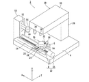
このウエーハ分離ステップは、例えば図9に示すような押圧機構54により実施する。押圧機構54は、コラム52内に内蔵された移動機構により上下方向に移動するヘッド56と、ヘッド56に対して、図9(B)に示すように、矢印R方向に回転される押圧部材58とを含んでいる。
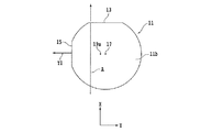
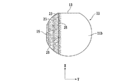
11 SiC基板
11a 第一の面(表面)
11b 第二の面(裏面)
13 第一のオリエンテーションフラット
15 第二のオリエンテーションフラット
17 第一の面の垂線
19 c軸
21 c面
23 改質層
25 クラック
26 支持テーブル
27 薄板(薄膜)
30 レーザービーム照射ユニット
36 集光器(レーザーヘッド)
54 押圧機構
56 ヘッド
58 押圧部材
Claims (5)
- 第一の面と該第一の面と反対側の第二の面と、該第一の面から該第二の面に至るc軸と、該c軸に直交するc面とを有するSiC基板の該第一の面にエピタキシャル成長によって積層された薄板をSiC基板から分離する薄板の分離方法であって、
SiC基板に対して透過性を有する波長のレーザービームの集光点を該第二の面からSiC基板の該第一の面近傍に位置付けると共に、該集光点とSiC基板とを相対的に移動して該レーザービームを該第二の面に照射し、該第一の面に平行な改質層及び該改質層から伸長するクラックを形成して分離起点を形成する分離起点形成ステップと、
該分離起点形成ステップを実施した後、外力を付与して該分離起点から該薄板をSiC基板から分離する分離ステップと、を備え、
該分離起点形成ステップは、該第二の面の垂線に対して該c軸がオフ角分傾き、該第二の面と該c面との間にオフ角が形成される方向と直交する方向にレーザービームの集光点を移動して直線状の改質層を形成する改質層形成ステップと、
該オフ角が形成される方向に該集光点を相対的に移動して所定量インデックスするインデックスステップと、
を含むことを特徴とする薄板の分離方法。 - 該分離起点形成ステップにおいて、該集光点は該薄板側に位置付けられ、該分離ステップを実施すると、SiC基板側に該薄板の一部が残存する請求項1記載の薄板の分離方法。
- 該分離起点形成ステップにおいて、該集光点はSiC基板側に位置付けられ、該分離ステップを実施すると、該薄板側にSiC基板の一部が残存する請求項1記載の薄板の分離方法。
- 該分離ステップを実施した後、SiC基板に残存する該薄板の一部を研削して除去する研削ステップを更に備えた請求項2記載の薄板の分離方法。
- 該分離ステップを実施した後、該薄板の裏面に残存するSiC基板の一部を研削して除去する研削ステップを更に備えた請求項3記載の薄板の分離方法。
Priority Applications (8)
| Application Number | Priority Date | Filing Date | Title |
|---|---|---|---|
| JP2015083642A JP6456228B2 (ja) | 2015-04-15 | 2015-04-15 | 薄板の分離方法 |
| TW105105705A TWI663015B (zh) | 2015-04-15 | 2016-02-25 | 薄板的分離方法 |
| MYPI2016701027A MY177241A (en) | 2015-04-15 | 2016-03-22 | Thin plate separating method |
| KR1020160033877A KR102309388B1 (ko) | 2015-04-15 | 2016-03-22 | 박판의 분리 방법 |
| SG10201602313YA SG10201602313YA (en) | 2015-04-15 | 2016-03-24 | Thin plate separating method |
| CN201610190979.2A CN106057737B (zh) | 2015-04-15 | 2016-03-30 | 薄板的分离方法 |
| DE102016205917.3A DE102016205917A1 (de) | 2015-04-15 | 2016-04-08 | Dünnplattenherstellungsverfahren |
| US15/098,945 US9941130B2 (en) | 2015-04-15 | 2016-04-14 | Thin plate separating method |
Applications Claiming Priority (1)
| Application Number | Priority Date | Filing Date | Title |
|---|---|---|---|
| JP2015083642A JP6456228B2 (ja) | 2015-04-15 | 2015-04-15 | 薄板の分離方法 |
Publications (2)
| Publication Number | Publication Date |
|---|---|
| JP2016207702A true JP2016207702A (ja) | 2016-12-08 |
| JP6456228B2 JP6456228B2 (ja) | 2019-01-23 |
Family
ID=57043702
Family Applications (1)
| Application Number | Title | Priority Date | Filing Date |
|---|---|---|---|
| JP2015083642A Active JP6456228B2 (ja) | 2015-04-15 | 2015-04-15 | 薄板の分離方法 |
Country Status (8)
| Country | Link |
|---|---|
| US (1) | US9941130B2 (ja) |
| JP (1) | JP6456228B2 (ja) |
| KR (1) | KR102309388B1 (ja) |
| CN (1) | CN106057737B (ja) |
| DE (1) | DE102016205917A1 (ja) |
| MY (1) | MY177241A (ja) |
| SG (1) | SG10201602313YA (ja) |
| TW (1) | TWI663015B (ja) |
Cited By (8)
| Publication number | Priority date | Publication date | Assignee | Title |
|---|---|---|---|---|
| KR20180119481A (ko) * | 2017-04-25 | 2018-11-02 | 가부시기가이샤 디스코 | SiC 웨이퍼의 생성 방법 |
| US10388526B1 (en) | 2018-04-20 | 2019-08-20 | Semiconductor Components Industries, Llc | Semiconductor wafer thinning systems and related methods |
| US10468304B1 (en) | 2018-05-31 | 2019-11-05 | Semiconductor Components Industries, Llc | Semiconductor substrate production systems and related methods |
| US10896815B2 (en) | 2018-05-22 | 2021-01-19 | Semiconductor Components Industries, Llc | Semiconductor substrate singulation systems and related methods |
| US11121035B2 (en) | 2018-05-22 | 2021-09-14 | Semiconductor Components Industries, Llc | Semiconductor substrate processing methods |
| US11264280B2 (en) | 2017-06-19 | 2022-03-01 | Rohm Co., Ltd. | Semiconductor device manufacturing method and wafer-attached structure |
| US11830771B2 (en) | 2018-05-31 | 2023-11-28 | Semiconductor Components Industries, Llc | Semiconductor substrate production systems and related methods |
| US11854889B2 (en) | 2018-05-24 | 2023-12-26 | Semiconductor Components Industries, Llc | Die cleaning systems and related methods |
Families Citing this family (13)
| Publication number | Priority date | Publication date | Assignee | Title |
|---|---|---|---|---|
| JP6429715B2 (ja) * | 2015-04-06 | 2018-11-28 | 株式会社ディスコ | ウエーハの生成方法 |
| JP6478821B2 (ja) * | 2015-06-05 | 2019-03-06 | 株式会社ディスコ | ウエーハの生成方法 |
| JP6781639B2 (ja) * | 2017-01-31 | 2020-11-04 | 株式会社ディスコ | ウエーハ生成方法 |
| JP6896344B2 (ja) * | 2017-09-22 | 2021-06-30 | 株式会社ディスコ | チップの製造方法 |
| US10940611B2 (en) | 2018-07-26 | 2021-03-09 | Halo Industries, Inc. | Incident radiation induced subsurface damage for controlled crack propagation in material cleavage |
| JP7235456B2 (ja) * | 2018-08-14 | 2023-03-08 | 株式会社ディスコ | 半導体基板の加工方法 |
| JP7128067B2 (ja) * | 2018-09-14 | 2022-08-30 | 株式会社ディスコ | ウエーハの生成方法およびレーザー加工装置 |
| US10562130B1 (en) | 2018-12-29 | 2020-02-18 | Cree, Inc. | Laser-assisted method for parting crystalline material |
| US11024501B2 (en) | 2018-12-29 | 2021-06-01 | Cree, Inc. | Carrier-assisted method for parting crystalline material along laser damage region |
| US10576585B1 (en) | 2018-12-29 | 2020-03-03 | Cree, Inc. | Laser-assisted method for parting crystalline material |
| US12525453B2 (en) * | 2019-04-19 | 2026-01-13 | Tokyo Electron Limited | Processing apparatus and processing method |
| JP7308652B2 (ja) * | 2019-04-26 | 2023-07-14 | 株式会社ディスコ | デバイスチップの製造方法 |
| US10611052B1 (en) | 2019-05-17 | 2020-04-07 | Cree, Inc. | Silicon carbide wafers with relaxed positive bow and related methods |
Citations (3)
| Publication number | Priority date | Publication date | Assignee | Title |
|---|---|---|---|---|
| JP2012146878A (ja) * | 2011-01-13 | 2012-08-02 | Hamamatsu Photonics Kk | レーザ加工方法 |
| WO2012108052A1 (ja) * | 2011-02-10 | 2012-08-16 | 信越ポリマー株式会社 | 単結晶基板製造方法および内部改質層形成単結晶部材 |
| JP2013049161A (ja) * | 2011-08-30 | 2013-03-14 | Hamamatsu Photonics Kk | 加工対象物切断方法 |
Family Cites Families (24)
| Publication number | Priority date | Publication date | Assignee | Title |
|---|---|---|---|---|
| FR2716303B1 (fr) * | 1994-02-11 | 1996-04-05 | Franck Delorme | Laser à réflecteurs de Bragg distribués, accordable en longueur d'onde, à réseaux de diffraction virtuels activés sélectivement. |
| JP2000094211A (ja) | 1998-09-22 | 2000-04-04 | Honda Motor Co Ltd | フライスカッタ |
| JP2000094221A (ja) | 1998-09-24 | 2000-04-04 | Toyo Advanced Technologies Co Ltd | 放電式ワイヤソー |
| JP2005268752A (ja) * | 2004-02-19 | 2005-09-29 | Canon Inc | レーザ割断方法、被割断部材および半導体素子チップ |
| JP4749799B2 (ja) * | 2005-08-12 | 2011-08-17 | 浜松ホトニクス株式会社 | レーザ加工方法 |
| US8728234B2 (en) | 2008-06-04 | 2014-05-20 | Sixpoint Materials, Inc. | Methods for producing improved crystallinity group III-nitride crystals from initial group III-nitride seed by ammonothermal growth |
| CN101663125B (zh) * | 2007-04-05 | 2012-11-28 | 查目工程股份有限公司 | 激光加工方法及切割方法以及具有多层基板的结构体的分割方法 |
| JP2009135448A (ja) * | 2007-11-01 | 2009-06-18 | Semiconductor Energy Lab Co Ltd | 半導体基板の作製方法及び半導体装置の作製方法 |
| JP2011040564A (ja) * | 2009-08-11 | 2011-02-24 | Toshiba Corp | 半導体素子の製造方法および製造装置 |
| JP2011077102A (ja) | 2009-09-29 | 2011-04-14 | Toyoda Gosei Co Ltd | ウエハ、iii族窒化物系化合物半導体素子、及びそれらの製造方法 |
| JP2011077325A (ja) | 2009-09-30 | 2011-04-14 | Sumitomo Electric Ind Ltd | Iii族窒化物半導体基板の製造方法 |
| JP2011165766A (ja) * | 2010-02-05 | 2011-08-25 | Disco Abrasive Syst Ltd | 光デバイスウエーハの加工方法 |
| JP5558128B2 (ja) * | 2010-02-05 | 2014-07-23 | 株式会社ディスコ | 光デバイスウエーハの加工方法 |
| JP2012238746A (ja) * | 2011-05-12 | 2012-12-06 | Disco Abrasive Syst Ltd | 光デバイスウエーハの分割方法 |
| JP5904720B2 (ja) * | 2011-05-12 | 2016-04-20 | 株式会社ディスコ | ウエーハの分割方法 |
| US9214353B2 (en) * | 2012-02-26 | 2015-12-15 | Solexel, Inc. | Systems and methods for laser splitting and device layer transfer |
| KR20140011071A (ko) * | 2012-07-17 | 2014-01-28 | 서울바이오시스 주식회사 | 질화물 반도체층과 성장 기판 분리 방법 |
| JP6180223B2 (ja) | 2013-08-06 | 2017-08-16 | 株式会社ディスコ | ウェーハの製造方法 |
| JP6358941B2 (ja) * | 2014-12-04 | 2018-07-18 | 株式会社ディスコ | ウエーハの生成方法 |
| JP6395633B2 (ja) * | 2015-02-09 | 2018-09-26 | 株式会社ディスコ | ウエーハの生成方法 |
| JP6425606B2 (ja) * | 2015-04-06 | 2018-11-21 | 株式会社ディスコ | ウエーハの生成方法 |
| JP6482389B2 (ja) * | 2015-06-02 | 2019-03-13 | 株式会社ディスコ | ウエーハの生成方法 |
| JP6472333B2 (ja) * | 2015-06-02 | 2019-02-20 | 株式会社ディスコ | ウエーハの生成方法 |
| JP6482423B2 (ja) * | 2015-07-16 | 2019-03-13 | 株式会社ディスコ | ウエーハの生成方法 |
-
2015
- 2015-04-15 JP JP2015083642A patent/JP6456228B2/ja active Active
-
2016
- 2016-02-25 TW TW105105705A patent/TWI663015B/zh active
- 2016-03-22 KR KR1020160033877A patent/KR102309388B1/ko active Active
- 2016-03-22 MY MYPI2016701027A patent/MY177241A/en unknown
- 2016-03-24 SG SG10201602313YA patent/SG10201602313YA/en unknown
- 2016-03-30 CN CN201610190979.2A patent/CN106057737B/zh active Active
- 2016-04-08 DE DE102016205917.3A patent/DE102016205917A1/de active Pending
- 2016-04-14 US US15/098,945 patent/US9941130B2/en active Active
Patent Citations (3)
| Publication number | Priority date | Publication date | Assignee | Title |
|---|---|---|---|---|
| JP2012146878A (ja) * | 2011-01-13 | 2012-08-02 | Hamamatsu Photonics Kk | レーザ加工方法 |
| WO2012108052A1 (ja) * | 2011-02-10 | 2012-08-16 | 信越ポリマー株式会社 | 単結晶基板製造方法および内部改質層形成単結晶部材 |
| JP2013049161A (ja) * | 2011-08-30 | 2013-03-14 | Hamamatsu Photonics Kk | 加工対象物切断方法 |
Cited By (17)
| Publication number | Priority date | Publication date | Assignee | Title |
|---|---|---|---|---|
| KR20180119481A (ko) * | 2017-04-25 | 2018-11-02 | 가부시기가이샤 디스코 | SiC 웨이퍼의 생성 방법 |
| KR102450902B1 (ko) | 2017-04-25 | 2022-10-04 | 가부시기가이샤 디스코 | SiC 웨이퍼의 생성 방법 |
| US11264280B2 (en) | 2017-06-19 | 2022-03-01 | Rohm Co., Ltd. | Semiconductor device manufacturing method and wafer-attached structure |
| US12148667B2 (en) | 2017-06-19 | 2024-11-19 | Rohm Co., Ltd. | Semiconductor device manufacturing method and wafer-attached structure |
| US11742243B2 (en) | 2017-06-19 | 2023-08-29 | Rohm Co., Ltd. | Semiconductor device manufacturing method and wafer-attached structure |
| US10388526B1 (en) | 2018-04-20 | 2019-08-20 | Semiconductor Components Industries, Llc | Semiconductor wafer thinning systems and related methods |
| US10665458B2 (en) | 2018-04-20 | 2020-05-26 | Semiconductor Components Industries, Llc | Semiconductor wafer thinning systems and related methods |
| US11152211B2 (en) | 2018-04-20 | 2021-10-19 | Semiconductor Components Industries, Llc | Semiconductor wafer thinning systems and related methods |
| US11823953B2 (en) | 2018-05-22 | 2023-11-21 | Semiconductor Components Industries, Llc | Semiconductor substrate processing methods |
| US11373859B2 (en) | 2018-05-22 | 2022-06-28 | Semiconductor Components Industries, Llc | Semiconductor substrate singulation systems and related methods |
| US11121035B2 (en) | 2018-05-22 | 2021-09-14 | Semiconductor Components Industries, Llc | Semiconductor substrate processing methods |
| US10896815B2 (en) | 2018-05-22 | 2021-01-19 | Semiconductor Components Industries, Llc | Semiconductor substrate singulation systems and related methods |
| US11854889B2 (en) | 2018-05-24 | 2023-12-26 | Semiconductor Components Industries, Llc | Die cleaning systems and related methods |
| US12230543B2 (en) | 2018-05-24 | 2025-02-18 | Semiconductor Components Industries, Llc | Die cleaning systems and related methods |
| US10770351B2 (en) | 2018-05-31 | 2020-09-08 | Semiconductor Components Industries, Llc | Semiconductor substrate production systems and related methods |
| US11830771B2 (en) | 2018-05-31 | 2023-11-28 | Semiconductor Components Industries, Llc | Semiconductor substrate production systems and related methods |
| US10468304B1 (en) | 2018-05-31 | 2019-11-05 | Semiconductor Components Industries, Llc | Semiconductor substrate production systems and related methods |
Also Published As
| Publication number | Publication date |
|---|---|
| MY177241A (en) | 2020-09-09 |
| TW201641206A (zh) | 2016-12-01 |
| SG10201602313YA (en) | 2016-11-29 |
| DE102016205917A1 (de) | 2016-10-20 |
| JP6456228B2 (ja) | 2019-01-23 |
| CN106057737B (zh) | 2021-06-29 |
| US20160307763A1 (en) | 2016-10-20 |
| US9941130B2 (en) | 2018-04-10 |
| TWI663015B (zh) | 2019-06-21 |
| CN106057737A (zh) | 2016-10-26 |
| KR20160123224A (ko) | 2016-10-25 |
| KR102309388B1 (ko) | 2021-10-05 |
Similar Documents
| Publication | Publication Date | Title |
|---|---|---|
| JP6456228B2 (ja) | 薄板の分離方法 | |
| KR102475682B1 (ko) | SiC 기판의 분리 방법 | |
| JP6472347B2 (ja) | ウエーハの薄化方法 | |
| JP6486239B2 (ja) | ウエーハの加工方法 | |
| JP6395634B2 (ja) | ウエーハの生成方法 | |
| JP6486240B2 (ja) | ウエーハの加工方法 | |
| KR102361278B1 (ko) | 웨이퍼의 생성 방법 | |
| JP6482425B2 (ja) | ウエーハの薄化方法 | |
| JP6391471B2 (ja) | ウエーハの生成方法 | |
| JP6395632B2 (ja) | ウエーハの生成方法 | |
| JP6358941B2 (ja) | ウエーハの生成方法 | |
| KR20220162659A (ko) | 웨이퍼의 생성 방법 | |
| JP6429715B2 (ja) | ウエーハの生成方法 | |
| JP6355540B2 (ja) | ウエーハの生成方法 | |
| KR20160143529A (ko) | 웨이퍼의 생성 방법 | |
| JP6472332B2 (ja) | ウエーハの生成方法 |
Legal Events
| Date | Code | Title | Description |
|---|---|---|---|
| A621 | Written request for application examination |
Free format text: JAPANESE INTERMEDIATE CODE: A621 Effective date: 20180221 |
|
| A977 | Report on retrieval |
Free format text: JAPANESE INTERMEDIATE CODE: A971007 Effective date: 20181207 |
|
| TRDD | Decision of grant or rejection written | ||
| A01 | Written decision to grant a patent or to grant a registration (utility model) |
Free format text: JAPANESE INTERMEDIATE CODE: A01 Effective date: 20181218 |
|
| A61 | First payment of annual fees (during grant procedure) |
Free format text: JAPANESE INTERMEDIATE CODE: A61 Effective date: 20181218 |
|
| R150 | Certificate of patent or registration of utility model |
Ref document number: 6456228 Country of ref document: JP Free format text: JAPANESE INTERMEDIATE CODE: R150 |
|
| R250 | Receipt of annual fees |
Free format text: JAPANESE INTERMEDIATE CODE: R250 |
|
| R250 | Receipt of annual fees |
Free format text: JAPANESE INTERMEDIATE CODE: R250 |
|
| R250 | Receipt of annual fees |
Free format text: JAPANESE INTERMEDIATE CODE: R250 |
|
| R250 | Receipt of annual fees |
Free format text: JAPANESE INTERMEDIATE CODE: R250 |
|
| R250 | Receipt of annual fees |
Free format text: JAPANESE INTERMEDIATE CODE: R250 |