JP2016100926A - Power conversion device - Google Patents
Power conversion device Download PDFInfo
- Publication number
- JP2016100926A JP2016100926A JP2014234076A JP2014234076A JP2016100926A JP 2016100926 A JP2016100926 A JP 2016100926A JP 2014234076 A JP2014234076 A JP 2014234076A JP 2014234076 A JP2014234076 A JP 2014234076A JP 2016100926 A JP2016100926 A JP 2016100926A
- Authority
- JP
- Japan
- Prior art keywords
- converter
- phase
- power converter
- energy storage
- circuit
- Prior art date
- Legal status (The legal status is an assumption and is not a legal conclusion. Google has not performed a legal analysis and makes no representation as to the accuracy of the status listed.)
- Granted
Links
- 238000006243 chemical reaction Methods 0.000 title claims abstract description 43
- 239000004065 semiconductor Substances 0.000 claims abstract description 58
- 238000004146 energy storage Methods 0.000 claims abstract description 31
- 238000007599 discharging Methods 0.000 claims description 12
- 238000012544 monitoring process Methods 0.000 claims description 11
- 238000005520 cutting process Methods 0.000 claims description 2
- 239000003990 capacitor Substances 0.000 description 89
- 238000010586 diagram Methods 0.000 description 13
- 238000004804 winding Methods 0.000 description 9
- 238000000926 separation method Methods 0.000 description 7
- 230000002159 abnormal effect Effects 0.000 description 3
- 230000000694 effects Effects 0.000 description 2
- 230000005284 excitation Effects 0.000 description 2
- 238000004519 manufacturing process Methods 0.000 description 2
- 238000000034 method Methods 0.000 description 2
- 230000003071 parasitic effect Effects 0.000 description 2
- 230000002265 prevention Effects 0.000 description 2
- 230000015556 catabolic process Effects 0.000 description 1
- 239000012141 concentrate Substances 0.000 description 1
- 239000004020 conductor Substances 0.000 description 1
- 238000009413 insulation Methods 0.000 description 1
- 230000000630 rising effect Effects 0.000 description 1
- 229920006395 saturated elastomer Polymers 0.000 description 1
- 238000004904 shortening Methods 0.000 description 1
- 238000003860 storage Methods 0.000 description 1
- 238000012795 verification Methods 0.000 description 1
Images


Abstract
Description
この発明は、半導体スイッチング素子とエネルギ蓄積要素とを有する複数の変換器セルを備えた電力変換装置に関するものである。 The present invention relates to a power conversion device including a plurality of converter cells each having a semiconductor switching element and an energy storage element.
近年、高圧・大容量用途の電力変換装置においては、主回路となる電力変換器としてマルチレベル変換器の実用化が図られている。
このような電力変換器では、電力変換器の交流端子U、V、Wに、複数台の変換器セルを直列に接続し、これらの変換器セルに内在する半導体スイッチング素子をオン/オフ制御する。変換器セルには、ブリッジセルと呼ばれるフルブリッジの回路が用いられる。そして、交流端子U、V、Wに発生する無効電力、あるいは有効電力を自由に制御することの可能なモジュラー・マルチレベル・カスケード変換器(Modular Multilevel Cascade Converter)が開示されている(例えば、非特許文献1参照)。
In recent years, in power converters for high-voltage and large-capacity applications, multi-level converters have been put to practical use as power converters serving as main circuits.
In such a power converter, a plurality of converter cells are connected in series to the AC terminals U, V, and W of the power converter, and the semiconductor switching elements included in these converter cells are on / off controlled. . A full-bridge circuit called a bridge cell is used for the converter cell. A modular multilevel cascade converter capable of freely controlling reactive power generated in the AC terminals U, V, and W or active power is disclosed (for example, non-multi-level cascade converter). Patent Document 1).
一方、複数台の変換器セルを、交流端子U、V、Wと直流端子との間に直列に接続し、これらの変換器セルに内在する半導体スイッチング素子をオン/オフ制御する。変換器セルには、チョッパセルと呼ばれるハーフブリッジの回路が用いられる。そして、交流端子U、V、Wには交流電圧を、直流端子には直流電圧を発生させることのできる回路構成のモジュラー・マルチレベル変換器が開示されている(例えば、非特許文献2参照)。 On the other hand, a plurality of converter cells are connected in series between the AC terminals U, V, W and the DC terminal, and the semiconductor switching elements inherent in these converter cells are controlled to be turned on / off. A half-bridge circuit called a chopper cell is used for the converter cell. And the modular multilevel converter of the circuit structure which can generate | occur | produce an alternating voltage to an alternating current terminal U, V, and W and a direct current voltage to a direct current terminal is disclosed (for example, refer nonpatent literature 2). .
さらに、前述のような変換器セルである変換器ユニット内のコンデンサを初期充電及び放電するため、以下の構成が開示されている。トランスは、スター結線で構成される一次巻線及び二次巻線と、デルタ結線で構成される三次巻線とを有する。一次巻線は交流遮断器を介して高電圧の交流電力系統に接続され、二次巻線は前記モジュラー・マルチレベル変換器の交流端子に接続され、三次巻線は、遮断器と初期充電及び放電用抵抗とを介して、低電圧の交流電源に接続される。3相短絡用スイッチが遮断器と初期充電及び放電用抵抗の間に設けられ、遮断器が3相交流電源側に設けられ、初期充電及び放電用抵抗がトランスの三次巻線側に設けられる(例えば、特許文献1参照)。 Furthermore, in order to initially charge and discharge a capacitor in a converter unit which is a converter cell as described above, the following configuration is disclosed. The transformer includes a primary winding and a secondary winding configured by star connection, and a tertiary winding configured by delta connection. The primary winding is connected to a high voltage AC power system through an AC circuit breaker, the secondary winding is connected to the AC terminal of the modular multilevel converter, and the tertiary winding is connected to the circuit breaker and the initial charge and It is connected to a low-voltage AC power supply via a discharging resistor. A three-phase short-circuit switch is provided between the circuit breaker and the initial charging and discharging resistor, a circuit breaker is provided on the three-phase AC power source side, and an initial charging and discharging resistor is provided on the tertiary winding side of the transformer ( For example, see Patent Document 1).
上記のような従来の電力変換装置では、電力変換器の交流端子を交流電源に接続して使用した際に、交流電源の電圧が正常範囲内から逸脱して過電圧となると、電力変換器の変換器セルに内在するエネルギ蓄積要素(例えばコンデンサ)の両端の電圧も過電圧となる。このような状態で変換器セル内の半導体スイッチング素子をスイッチング動作させ続けると、半導体スイッチング素子がオン状態からオフ状態に変化するターンオフの際に発生するサージ電圧が、エネルギ蓄積要素の両端の電圧に重畳される。このようにエネルギ蓄積要素の両端の電圧が上昇している状態にも関わらず、半導体スイッチング素子をスイッチング動作し続けることで、半導体スイッチング素子に印加される電圧が、半導体スイッチング素子の耐圧を超過して素子を破損してしまう可能性がある。 In the conventional power converter as described above, when the AC terminal of the power converter is connected to the AC power source and the voltage of the AC power source deviates from the normal range and becomes an overvoltage, the conversion of the power converter is performed. The voltage across the energy storage element (eg, capacitor) inherent in the vessel cell is also an overvoltage. If the semiconductor switching element in the converter cell continues to be switched in such a state, the surge voltage generated at the time of turn-off in which the semiconductor switching element changes from the on state to the off state becomes the voltage across the energy storage element. Superimposed. In this way, the voltage applied to the semiconductor switching element exceeds the breakdown voltage of the semiconductor switching element by continuing the switching operation of the semiconductor switching element in spite of the state where the voltage across the energy storage element is rising. May damage the device.
このような問題点を回避する為には、エネルギ蓄積要素の電圧が過電圧になると電力変換装置の運転を停止させる。上記非特許文献1、2記載の電力変換装置では交流電源の電圧が正常に戻っても、エネルギ蓄積要素を速やかに正常電圧範囲まで放電させて電力変換装置を再起動するのは困難であった。
In order to avoid such problems, the operation of the power converter is stopped when the voltage of the energy storage element becomes an overvoltage. In the power converters described in
上記特許文献1に記載の電力変換装置では、エネルギ蓄積要素であるコンデンサを放電するために、初期充電及び放電用抵抗を用いた放電用回路を、変圧器と交流電源との間に設けている。
しかし、コンデンサの放電電流を放電用回路に流すための経路切替用の短絡用スイッチや、放電用回路の経路も別途必要になり、装置構成が大型化して信頼性が低下するものであった。
In the power conversion device described in
However, a short-circuit switch for switching the path for flowing the discharge current of the capacitor to the discharge circuit and a path for the discharge circuit are also required separately, which increases the size of the apparatus and reduces the reliability.
この発明は上述のような課題を解決するためになされたものであり、電力変換装置が備えるエネルギ蓄積要素を速やかに放電することができ、且つ装置構成の小型化および低コスト化が可能で、信頼性の高い電力変換装置の提供を目的とする。 The present invention has been made to solve the above-described problems, and can quickly discharge the energy storage element included in the power conversion device, and can reduce the size and cost of the device configuration. An object is to provide a highly reliable power conversion device.
この発明に係る電力変換装置は、多相交流回路の各相にそれぞれ接続された複数の相アームを有する電力変換器と、制御装置とを備え、前記相アームは、それぞれエネルギ蓄積要素と半導体スイッチング素子とを有する変換器セルを、1あるいは複数直列接続して備え、前記電力変換器は、前記電力変換器内で前記変換器セルを介して流れる循環電流の経路内に直列接続され、前記エネルギ蓄積要素の放電に用いる抵抗と、前記抵抗に並列接続され前記抵抗をバイパスする第1バイパススイッチとを備えたものである。 The power conversion device according to the present invention includes a power converter having a plurality of phase arms respectively connected to each phase of a multiphase AC circuit, and a control device, wherein the phase arms are respectively energy storage elements and semiconductor switching devices. One or a plurality of converter cells having an element connected in series, wherein the power converter is connected in series in a path of a circulating current flowing through the converter cell in the power converter, and the energy converter A resistor used for discharging the storage element, and a first bypass switch connected in parallel to the resistor and bypassing the resistor.
この発明に係る電力変換装置によれば、電力変換装置が備えるエネルギ蓄積要素を速やかに放電し、且つ装置構成の小型化および低コスト化が可能で、信頼性の高い電力変換装置を提供することができる。 According to the power conversion device of the present invention, it is possible to quickly discharge the energy storage element included in the power conversion device, and to provide a highly reliable power conversion device that can reduce the size and cost of the device configuration. Can do.
実施の形態1.
以下、本発明の実施の形態1による電力変換装置100について図を用いて説明する。
図1は、本発明の実施の形態1による電力変換装置100を示す概略構成図である。
電力変換装置100は、多相交流回路である3相交流電源(以下、交流回路1と称す)に接続されて電力変換を行う電力変換器30と、電力変換器30の動作を制御する制御装置50とを備える。
Hereinafter,
FIG. 1 is a schematic configuration diagram showing a
図1に示すように、電力変換器30は、U相、V相、W相の3つの相アーム20をデルタ結線状に接続して構成されている。各相アーム20は、直列に接続された複数の変換器セル10を備えており、複数の変換器セル10にリアクトル3と抵抗40とがさらに直列に接続されている。さらに抵抗40には、この抵抗40をバイパスするためのスイッチである第1バイパススイッチ41が並列に接続されている。
各相アーム20は、変圧器2を介して交流回路1の各相の交流端子U、V、Wにそれぞれ接続されており、変圧器2と交流回路1との間には、電力変換器30と交流回路1とを切り離して電流を遮断するための切離スイッチ42が直列に接続されている。
As shown in FIG. 1, the
Each
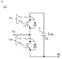
図2は、本発明の実施の形態1による電力変換器30内の各変換器セル10の回路構成図である。
図に示すように、変換器セル10は、半導体スイッチング素子16a、16b、16c、16dに、各々還流ダイオード17a、17b、17c、17dが逆並列に接続された半導体素子15a、15b、15c、15dと、エネルギ蓄積要素ESとを備えたフルブリッジ回路である。
半導体素子15cと半導体素子15dとの接続点には、変換器セル10の出力端子Poを、半導体素子15aと半導体素子15bとの接続点には、変換器セル10の出力端子Noを設ける。図1に示すように、変換器セル10の出力端子Poは、他の変換器セル10の出力端子Noへ接続される。
FIG. 2 is a circuit configuration diagram of each
As shown in the figure, the
An output terminal Po of the
図3は、変換器セル10の出力電圧と、半導体スイッチング素子16a〜16dとのスイッチング状態の関係を示す図である。
図に示すように、半導体スイッチング素子16a〜16dをオン/オフさせることで、変換器セル10の出力端子間には、コンデンサ11の両端の正電圧か、負電圧か、零電圧のいずれかを出力することができる。
例えば、半導体スイッチング素子16cと16bがオン、16dと16aがオフの場合では、コンデンサ11の両端の正電圧が出力される。
また例えば、半導体スイッチング素子16dと16aがオン、16cと16bがオフの場合では、コンデンサ11の両端の負電圧が出力される。
また例えば、半導体スイッチング素子16cと16aがオン、16dと16bがオフの場合では零電圧が出力され、半導体スイッチング素子16dと16bがオン、16cと16aがオフの場合も零電圧が出力される。
各スイッチング状態の切替時には、デッドタイムと呼ばれる短絡防止期間を入れてもよい。
FIG. 3 is a diagram illustrating the relationship between the output voltage of the
As shown in the figure, by turning on / off the semiconductor switching elements 16a to 16d, a positive voltage, a negative voltage, or a zero voltage between both ends of the
For example, when the
For example, when the
Further, for example, when the
When switching each switching state, a short-circuit prevention period called dead time may be inserted.
制御装置50は、各変換器セル10がそれぞれ備えるエネルギ蓄積要素ESの両端の電圧Vdcを監視する監視部51を備えている。
さらに制御装置50内には、電圧Vdcを判定する為の基準電圧Vbと、交流回路1の電圧Vacを判定するための電圧Vacbとが予め設定されている。
The
Further, in the
上記のエネルギ蓄積要素ESとして、ここでは例としてコンデンサ11を用いる。
また、上記の半導体スイッチング素子16a、16b、16c、16dには、IGBT(Insulated−Gate Bipolar Transistor)やGCT(Gate Commutated Turn−off thyristor)、MOSFET(Metal−Oxide−Semiconductor Field−Effect Transistor)などの半導体スイッチング素子を使用する。
また、電流容量に応じて各半導体素子15a、15b、15c、15dは、それぞれ複数素子を並列に接続して用いてもよい。
また、上記の切離スイッチ42および第1バイパススイッチ41は、開閉器でも良いし遮断器でも良い。
なお、上記の変圧器2は必ずしも必要ではなく、電圧調整や絶縁が不要であれば省略することができる。その場合、変圧器2の漏れインダクタンスの代わりにリアクトルを接続してもよい。
As the energy storage element ES, a
The
Further, according to the current capacity, each of the
Further, the
In addition, said
以下、本発明の実施の形態1による電力変換装置100の制御動作について説明する。
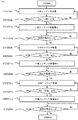
図4は、本発明の実施の形態1による電力変換装置100の制御動作を示すフロー図である。
電力変換装置100の運転を開始する際、制御装置50は、開閉指令50bにより第1バイパススイッチ41を開状態に制御する(STEP001)。
次に、制御装置50は、開閉指令50cにより切離スイッチ42を閉状態に制御して、電力変換器30を交流回路1に接続する(STEP002)。
これにより、交流回路1から抵抗40を介して各変換器セル10内のコンデンサ11に充電電流が流れ、コンデンサ11は初期充電される。この初期充電時に発生する突入電流は抵抗40により抑制される。
次に、制御装置50は、開閉指令50bにより第1バイパススイッチ41を閉状態に制御して、抵抗40をバイパスさせる(STEP003)。
次に、制御装置50は、スイッチング指令50aにより変換器セル10内の半導体スイッチング素子16a、16b、16c、16dをオン、オフさせるスイッチング動作を行って変換器セル10の出力を制御し、電力変換器30から交流電力(無効電力)を出力する(STEP004)。
Hereinafter, the control operation of
FIG. 4 is a flowchart showing a control operation of
When starting the operation of the
Next, the
Thereby, a charging current flows from the
Next, the
Next, the
STEP004の電力変換装置100の通常運転中において、交流回路1の電圧が正常範囲を逸脱して過電圧となった場合では、その影響をうけて変換器セル10が備えるコンデンサ11の電圧Vdcも過電圧となる。
制御装置50は、図示しない電圧センサにより検出された複数のコンデンサ11の両端の電圧Vdcを監視部51により監視し、少なくとも1つのコンデンサ11の両端の電圧Vdcが、予め設定された基準電圧Vbを超過して過電圧となった際には、電力変換器30の異常状態と判定する(STEP005、Yes)
基準電圧Vbとは、コンデンサ11の電圧Vdcがこの基準電圧Vbを超えた場合に、制御装置50が異常とみなす電圧値である。
During normal operation of the
The
The reference voltage Vb is a voltage value that the
次に、制御装置50は、スイッチング指令50aにより電力変換器30内の全ての半導体スイッチング素子16a、16b、16c、16dをオフにして(この状態をゲートブロック状態と呼ぶ)、電力変換器30の交流出力を停止する(STEP006)。
Next, the
次に、制御装置50は、開閉指令50cにより切離スイッチ42を開状態に制御して、電力変換器30を交流回路1から切り離す(STEP007)。
次に、制御装置50は、開閉指令50bにより抵抗40をバイパスしていた第1バイパススイッチ41を開状態に制御する(STEP008)。
Next, the
Next, the
次に、制御装置50は、スイッチング指令50aにより電力変換器30内の全ての変換器セル10が、コンデンサ11の両端の正または負の電圧の出力状態を維持するように制御する(STEP009)。
このように、電力変換器30を交流回路1から切り離した上で、全ての変換器セル10が正または負の電圧の出力状態を維持するように変換器セル10を制御する。これにより、デルタ結線にて形成された電力変換器30の循環電流の経路内に、抵抗40を介してコンデンサ11からの放電電流を流して、コンデンサ11のエネルギを放電させることができる。
こうして、コンデンサ11の両端の電圧Vdcを速やかに基準電圧Vb以下の正常範囲内まで下げることができる。
なお、STEP009においては、全ての変換器セル10の出力電圧が同一極性(同一方向)となるように制御している。
Next, the
In this way, after the
In this way, the voltage Vdc across the
In STEP 009, the output voltages of all the
次に、制御装置50は、監視部51により、コンデンサ11の両端の電圧Vdcが、基準電圧Vb以下の正常範囲内であることを確認する(STEP010、Yes)。
次に、制御装置50は、スイッチング指令50aにより、変換器セル10の正または負の電圧の出力状態を維持する制御を停止させて全ての半導体スイッチング素子16a〜16dをオフし、コンデンサ11の放電を停止する(STEP011)。
Next, the
Next, the
次に、制御装置50は、交流回路1の電圧Vacが電圧Vacb以下の正常範囲内であることを確認する(STEP012、Yes)。
電圧Vacbとは、交流回路1の電圧値であり、電力変換装置100が通常動作を継続しうる正常電圧範囲に基づく電圧値である。通常、交流回路1の電圧状態などによって設計される。
Next, the
The voltage Vacb is a voltage value of the
次に、制御装置50は、開閉指令50cにより切離スイッチ42を閉状態に制御して、交流回路1と電力変換器30とを接続する(STEP013)。
次に、制御装置50は、開閉指令50bにより第1バイパススイッチを閉状態に制御して、抵抗40をバイパスする(STEP014)。
次に、制御装置50は、スイッチング指令50aにより、電力変換器30の通常動作時のスイッチング動作を再開させ、電力変換器30から交流電力を出力して電力変換装置100の通常運転を開始する(STEP015)。
Next, the
Next, the
Next, in response to the switching
なお、上記STEP010において、検出されたコンデンサ11の両端の電圧Vdcが、監視部51により基準電圧Vbを超えて正常範囲外と判定された場合は(STEP010、No)、STEP009に戻り、引き続きコンデンサ11を放電させる。
In step 010, if the detected voltage Vdc across the
なお、上記のSTEP009のコンデンサ11の放電時において、各変換器セル10に流れる最大電流Imaxは、
最大電流Imax=(基準電圧Vb×変換器セル10の数)/(抵抗40の抵抗値R×抵抗40の数)
で導出できる。
抵抗40は、この最大電流Imaxが、変換器セル10内の半導体素子15a〜15dの定格電流以下になるように抵抗値Rを選定する。これにより、半導体素子15a〜15dを破損する恐れがない。
Note that the maximum current Imax flowing through each
Maximum current Imax = (reference voltage Vb × number of converter cells 10) / (resistance value R of
Can be derived.
The
上記のように構成された本実施の形態の電力変換装置100によると、電力変換器30内の変換器セル10のコンデンサ11の両端の電圧Vdcが過電圧となった異常状態では、電力変換器30の出力を停止させた上で、電力変換器30を交流回路1から切り離す。そして、コンデンサ11が放電するように変換器セル10の正または負の出力状態を維持することで、電力変換器30内で変換器セル10を介して流れる循環電流の経路に、コンデンサ11から放電された電流を流す。これにより、この循環電流の経路内に直列接続された抵抗40によってコンデンサ11のエネルギを放電させることが可能になる。
According to the
また、交流回路1の電圧が正常範囲内に戻った場合には、早急な電力変換装置100の再起動が要求される。
本実施の形態による電力変換装置100では、循環電流の経路内に抵抗40を設け、コンデンサ11を放電させるように変換器セル10を制御するため、コンデンサ11の電圧Vdcを速やかに正常範囲内まで下げることができる。このため、交流回路1の電圧が正常範囲内に復帰した場合に、直ちに電力変換装置100を再起動して交流回路1に接続させることができるため、所望の無効電力を出力できない期間を短縮することができる。
Further, when the voltage of the
In
また、コンデンサ11の両端の電圧Vdcが高い状態で、半導体スイッチング素子16a〜16dをターンオフスイッチングすることがなく、過電圧による半導体素子15a〜15dの破損を回避することができる。
In addition, the semiconductor switching elements 16a to 16d are not turned off when the voltage Vdc across the
また、上述したように、コンデンサ11は完全に放電せず、コンデンサ11の両端の電圧Vdcが基準電圧Vb以下になった時点で、コンデンサ11の放電を停止する上記STEP011の制御に移行する。このため、電力変換装置100の再起動において、起動時間をさらに短縮することができる。
Further, as described above, the
また、本実施の形態による電力変換装置100は、予め電力変換器30内に存在する循環電流が流れる経路を用いてコンデンサ11の放電を行うものなので、放電用の経路を別途設ける必要がなく、そのための追加の設備も不要である。
さらに、コンデンサ11を放電するための抵抗40を、コンデンサ11の初期充電用抵抗にも利用するため、使用する部品数が少なく、信頼性を向上させることができ、また小型化が可能で製造安価である。
なお、本実施の形態では、U相、V相、W相の全ての相アーム20にそれぞれ抵抗40を配置した例を挙げて説明しているが、この形態に限るものではなく、少なくとも一つの抵抗40が、電力変換器30の循環電流の経路内に直列に接続されていればよい。
In addition, since the
Further, since the
In the present embodiment, the example in which the
なお、上記STEP009では、全ての変換器セル10のコンデンサ11を放電状態にした。しかしながら、全ての変換器セル10のコンデンサ11を放電状態にする制御に限るものではない。例えば、過電圧となった変換器セル10のコンデンサ11のみを正または負の電圧の出力状態にして放電し、その他の変換器セル10を零電圧の出力状態にしてもよい。この場合、過電圧状態でないコンデンサ11を放電しないため、電力変換装置100の再起動時において、起動時間をさらに短縮することができる。
In STEP 009, the
また、上記のSTEP005では、複数のコンデンサ11の両端の電圧Vdcのうちで、少なくとも1つのコンデンサ11の両端の電圧Vdcが、基準電圧Vbを超過したかどうかの判定を行ったが、これに限るものではない。例えば複数のコンデンサ11の両端の電圧Vdcの平均値を用いて判定するものでもよく、また例えば、基準となる任意の変換器セル10を選出し、その両端の電圧Vdcで判定するものでもよい。
また、上記のSTEP002とSTEP003、STEP007とSTEP008およびSTEP013とSTEP014の制御順番は逆でもよい。
In STEP 005 described above, it is determined whether or not the voltage Vdc at both ends of at least one
Also, the control order of STEP002 and STEP003, STEP007 and STEP008, and STEP013 and STEP014 may be reversed.
実施の形態2.
以下、この発明の実施の形態2を、上記実施の形態1と異なる箇所を中心に図を用いて説明する。上記実施の形態1と同様の部分は同一符号を付して説明を省略する。
図5は、本発明の実施の形態2による電力変換装置200を示す概略構成図である。
電力変換装置200は、直流と交流との間で電力変換を行う電力変換器230と、電力変換器230の動作を制御する制御装置50とを備える。
The second embodiment of the present invention will be described below with reference to the drawings, focusing on the differences from the first embodiment. The same parts as those in the first embodiment are denoted by the same reference numerals and the description thereof is omitted.
FIG. 5 is a schematic configuration diagram showing a
The
図5に示す様に、電力変換器230は、正側直流母線4Pに接続される相アームである正側相アーム220Pと、負側直流母線4Nに接続される相アームである負側相アーム220Nとを直列接続して構成したU相、V相、W相の3つのレグ回路225を備えている。
各正側相アーム220Pおよび負側相アーム220Nは、直列に接続された複数の変換器セル210を備えている。正側相アーム220Pが備える複数の変換器セル210には、リアクトル203Pと抵抗40とがさらに直列に接続されており、負側相アーム220Nが備える複数の変換器セル210には、リアクトル203Nと抵抗40とがさらに直列に接続されている。さらに各抵抗40には、この抵抗40をバイパスするためのスイッチである第1バイパススイッチ41が並列に接続されている。
As shown in FIG. 5, the
Each positive
U相、V相、W相のレグ回路225は、正側直流母線4Pと負側直流母線4Nとの間に並列に接続されている。各相の正側相アーム220Pと負側相アーム220Nとの接続点は、それぞれ変圧器2を介して3相の交流回路1の各相の交流端子U、V、Wに接続されている。変圧器2と交流回路1との間には、電力変換器230と交流回路1とを切り離して電流を遮断するための切離スイッチ42が直列に接続される。また電力変換器230と直流端子P、Nとの間には、直流端子P、Nに接続される直流電源などの直流回路(図示せず)と電力変換器230とを切り離して電流を遮断するための切離スイッチ244が直列に接続されている。
The U-phase, V-phase, and W-
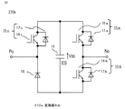
図6は、本発明の実施の形態2による電力変換器230内の各変換器セル210の回路構成図である。
図に示すように、変換器セル210は、半導体スイッチング素子16c、16dに、各々還流ダイオード17c、17dが逆並列に接続された半導体素子15c、15dと、コンデンサ11とを備えたハーフブリッジ回路である。
半導体素子15cと半導体素子15dとの接続点には、変換器セル210の出力端子Poを、コンデンサ11の負側には、変換器セル210の出力端子Noを設ける。
図5に示すように、変換器セル210の出力端子Poは、他の変換器セル210の出力端子Noへ接続される。
なお、半導体素子15c、15dには、電流容量に応じてそれぞれ複数の半導体素子を並列に接続して用いてもよい。また、上記の切離スイッチ244は、開閉器でも良いし遮断器でも良い。
FIG. 6 is a circuit configuration diagram of each
As shown in the figure, the
An output terminal Po of the
As shown in FIG. 5, the output terminal Po of the
A plurality of semiconductor elements may be connected in parallel to the
図7は、本発明の実施の形態2による変換器セル210の出力電圧と、半導体スイッチング素子16c、16dのスイッチング状態の関係を示す図である。
図に示すように、半導体スイッチング素子16c、16dをオン/オフさせることで、変換器セル210の出力端子Po、No間には、コンデンサ11の両端の正電圧か零電圧のいずれかを出力することができる。
例えば、半導体スイッチング素子16cがオン、16dがオフの場合では、コンデンサ11の両端の正電圧が出力される。
また例えば、半導体スイッチング素子16dがオン、16cがオフの場合は、零電圧が出力される。
各スイッチング状態の切替時には、デッドタイムと呼ばれる短絡防止期間を入れてもよい。
FIG. 7 is a diagram showing the relationship between the output voltage of
As shown in the figure, by turning on / off the
For example, when the
Further, for example, when the
When switching each switching state, a short-circuit prevention period called dead time may be inserted.
また、制御装置50の監視部51は、実施の形態1と同様に各変換器セル210がそれぞれ備えるコンデンサ11の両端の電圧Vdcを監視する。
Further, the
以下、本発明の実施の形態2による電力変換装置200の制御動作について説明する。
図8は、本発明の実施の形態2による電力変換装置の制御動作を示すフロー図である。
実施の形態1で示したSTEP001〜STEP008、STEP012〜STEP015までの制御動作は、後述の異なる点を除いては、本実施の形態についてもほぼ同様のものであり、図8においての図示は便宜上省略する。
Hereinafter, the control operation of the
FIG. 8 is a flowchart showing a control operation of the power conversion device according to the second embodiment of the present invention.
The control operation from STEP001 to STEP008 and STEP012 to STEP015 shown in the first embodiment is almost the same as that of the present embodiment except for different points described later, and the illustration in FIG. 8 is omitted for convenience. To do.
まず、STEP001〜STEP008において、実施の形態1と異なる点を以下に述べる。
STEP002において、本実施の形態では、開閉指令50cにより切離スイッチ42と切離スイッチ244とを閉状態に制御する。切離スイッチ244に対する開閉指令50cの図示は便宜上省略する。
First, differences from
In STEP002, in this embodiment, the
またSTEP004において、本実施の形態では、制御装置50は、変換器セル210内の半導体スイッチング素子16c、16dをオン、オフさせるスイッチング動作を行って変換器セル210の出力を制御し、交流端子U、V、Wには交流電圧を、直流端子P、Nには直流電圧を発生させる。
STEP006において、本実施の形態では、電力変換器230の全変換器セル210の半導体スイッチング素子16c、16dをオフして出力を停止する。
STEP007において、制御装置50は、切離スイッチ42と切離スイッチ244とを開状態に制御する。
In STEP 004, in the present embodiment, the
In STEP 006, in this embodiment, the
In STEP007, the
制御装置50は、図4に示すSTEP001〜STEP008を経て、コンデンサ11の電圧Vdcが基準電圧Vbを超過する過電圧時には電力変換器230の出力を停止させ、電力変換器230を、交流回路1と直流回路(直流端子P、N)とから切り離す。
The
次に、制御装置50は、U相を選択して、スイッチング指令50aによりU相のレグ回路225が備える全ての変換器セル210が、コンデンサ11の両端の正電圧の出力状態を維持するように制御する。そして、その他のV相およびW相のレグ回路225が備える全ての変換器セル210が零電圧の出力状態を維持するように制御する。(STEP2009a)。
このように、U相の変換器セル210のみを出力状態に制御する理由を説明する。例えば、U相、V相、W相の全ての変換器セル210を出力状態にすると、変換器セル210のコンデンサ11の両端の電圧が略等しい場合には、抵抗40に印加される電圧は略零となる。そのため、放電電流が流れず、コンデンサ11を放電することができないからである。
本実施の形態では、抵抗40に電圧が印加されるように、放電対象の相の変換器セル210のみを正の出力状態とし、その他の2相の変換器セル210の直流回路を零出力状態に制御する。
Next, the
The reason why only the
In the present embodiment, only the
こうして、電力変換器230を交流回路1と直流回路とから切り離した上で、U相のレグ回路225と、V相およびW相のレグ回路225との間に電位差を生じさせることにより、抵抗40に電圧が印加される。これにより、U相のレグ回路225と他の2相のレグ回路225との間に、抵抗40を介してU相のコンデンサ11からの放電電流を流して、U相の全てのコンデンサ11のエネルギを放電させることができる。
こうして、U相の全てのコンデンサ11の両端の電圧Vdcを速やかに基準電圧Vb以下の正常範囲内まで下げることができる。
In this way, the
In this way, the voltage Vdc at both ends of all the
次に、制御装置50は、監視部51により、U相の各コンデンサ11の両端の電圧Vdcが、基準電圧Vb以下の正常範囲内であることを判定する(STEP2010a、Yes)。
次に、制御装置50は、スイッチング指令50aによりU相の全ての変換器セル210の正電圧の出力状態を維持する制御を停止させて全変換器セル210半導体スイッチング素子16c、16dをオフし、U相のコンデンサ11の放電を停止する(STEP2011a)。
次に、制御装置50は、図示しない電流センサにより、抵抗40を流れる電流Icが、零となったことを確認する(STEP2050a、Yes)。
Next, the
Next, the
Next, the
次に、制御装置50は、V相を選択して、スイッチング指令50aによりV相のレグ回路225が備える全ての変換器セル210が、コンデンサ11の両端の正電圧の出力状態を維持するように制御する。そして、その他のU相およびW相のレグ回路225が備える全ての変換器セル210が零電圧の出力状態を維持するように制御する(STEP2009b)。
これにより、V相のレグ回路225と他の2相のレグ回路225との間に、抵抗40を介してV相のコンデンサ11からの放電電流を流して、V相の全てのコンデンサ11のエネルギを放電させることができる。
Next, the
As a result, the discharge current from the V-
次に、制御装置50は、監視部51により、V相の各コンデンサ11の両端の電圧Vdcが、基準電圧Vb以下の正常範囲内であることを判定する(STEP2010b、Yes)。
次に、制御装置50は、スイッチング指令50aによりV相の全ての変換器セル210の正電圧の出力状態を維持する制御を停止させて全変換器セル210の半導体スイッチング素子16c、16dをオフし、V相のコンデンサ11の放電を停止する(STEP2011b)。
次に、制御装置50は、図示しない電流センサにより、抵抗40を流れる電流Icが、零となったことを確認する(STEP2050b、Yes)。
Next, the
Next, the
Next, the
次に、制御装置50は、W相を選択して、スイッチング指令50aによりW相のレグ回路225が備える全ての変換器セル210が、コンデンサ11の両端の正電圧の出力状態を維持するように制御する。そして、その他のU相およびV相のレグ回路225が備える全ての変換器セル210が零電圧の出力状態を維持するように制御する(STEP2009c)。
これにより、W相のレグ回路225と他の2相のレグ回路225との間に、抵抗40を介してW相のコンデンサ11からの放電電流を流して、W相の全てのコンデンサ11のエネルギを放電させることができる。
Next, the
As a result, the discharge current from the W-
次に、制御装置50は、監視部51により、W相の各コンデンサ11の両端の電圧Vdcが、基準電圧Vb以下の正常範囲内であることを判定する(STEP2010c、Yes)。
次に、制御装置50は、スイッチング指令50aによりW相の全ての変換器セル210の正電圧の出力状態を維持する制御を停止させて全変換器セル210の半導体スイッチング素子16c、16dをオフし、W相のコンデンサ11の放電を停止する(STEP2011c)。
次に、制御装置50は、図示しない電流センサにより、抵抗40を流れる電流Icが、零となったことを確認する(STEP2050c、Yes)。
Next, the
Next, the
Next, the
次に、制御装置50は、図4に示すSTEP012以降の制御動作に移行するが、その制御動作で実施の形態1と異なる点を以下に述べる。
STEP013において、本実施の形態では、切離スイッチ42と切離スイッチ244とを閉状態に制御する。
Next, the
In STEP013, in this embodiment, the
またSTEP015において、本実施の形態では、制御装置50は、電力変換器230から交流電圧と直流電圧とを発生させる。
こうして、制御装置50は、図4に示すSTEP012〜STEP015を経て、電力変換器230を、交流回路1と直流回路とに接続し、電力変換器230の交流出力と直流出力とを開始する。
In STEP015, in the present embodiment,
In this way, the
なお、上記のSTEP2009a、2009b、2009cのコンデンサ11の放電時において、各変換器セル210に流れる最大電流Imaxは、
最大電流Imax=(基準電圧Vb×出力状態の変換器セル210の数)/(放電経路内の等価抵抗値Re)
で導出できる。
等価抵抗値Reは、上記STEP2009a〜2050cのような場合は、
等価抵抗値Re=抵抗40の抵抗値R×(2+(2/2))=抵抗40の抵抗値R×3
で導出できる。
抵抗40は、この最大電流Imaxが、変換器セル210内の半導体素子15c、15dの定格電流以下になるように選定する。これにより半導体素子15c、15dを破損する恐れがない。
It should be noted that the maximum current Imax flowing through each
Maximum current Imax = (reference voltage Vb × number of
Can be derived.
The equivalent resistance value Re is as in STEP 2009a to 2050c above.
Equivalent resistance value Re = resistance value R of
Can be derived.
The
また、上記の制御例では、制御装置は始めにU相を選択して、U相のレグ回路225が備えるコンデンサ11を放電し、次にV相を選択してV相のコンデンサ11を放電し、次にW相を選択してW相のコンデンサ11の放電を行ったが、選択する相の順番はこれに限るものではない。
In the above control example, the control device first selects the U phase, discharges the
上記のように構成された本実施の形態の電力変換装置200によると、上記実施の形態1と同様の効果を奏し、循環電流の経路内に抵抗40を設け、コンデンサ11を放電させるように変換器セル210を制御するため、コンデンサ11の電圧Vdcを速やかに正常範囲内まで下げることができる。このため、交流回路1の電圧が正常範囲内に復帰した場合に、直ちに電力変換装置200を再起動して交流回路1と直流回路とに接続させることができる。
According to the
また、予め電力変換器230内に存在する循環電流が流れる経路を用いてコンデンサ11の放電を行うものなので、放電用の経路を別途設ける必要がなく、そのための追加の設備も不要である。
さらに、コンデンサ11を放電するための抵抗40を、コンデンサ11の初期充電用抵抗にも利用するため、使用する部品数が少なく、信頼性を向上させることができ、また小型化が可能で製造安価である。
なお、本実施の形態では、U相、V相、W相の全ての正側相アーム220Pおよび負側相アーム220にNそれぞれ抵抗40を配置した例を挙げて説明しているが、この形態に限るものではなく、少なくとも一つの抵抗40が、電力変換器230の循環電流の経路内に直列に接続されていれば、コンデンサ11の放電に用いることができる。
In addition, since the
Further, since the
In the present embodiment, an example in which resistors 40 are arranged in each of the
なお、上記STEP2009a、2009b、2009cでは、各レグ回路225内の全ての変換器セル210のコンデンサ11を放電状態にした。しかしながら、各レグ回路225内の全ての変換器セル210のコンデンサ11を放電状態にする制御に限るものではない。例えば、過電圧となった変換器セル210のコンデンサ11のみを正の電圧の出力状態にして放電し、その他の変換器セル210を零電圧の出力状態にしてもよい。この場合、過電圧状態でないコンデンサ11を放電しないため、電力変換装置200の再起動時において、起動時間をさらに短縮することができる。
In STEP 2009a, 2009b, and 2009c, the
また、上述した制御では、1相を順次選択して、選択された相を順次放電したが、これに限るものではない。コンデンサ11を放電するように出力状態に制御される変換器セル210の数を、レグ回路225間で電位差が生じるように決定することで、抵抗40を介して放電電流を流すことができ、コンデンサ11は放電される。
In the above-described control, one phase is sequentially selected, and the selected phase is sequentially discharged. However, the present invention is not limited to this. By determining the number of
本実施の形態では、図6に示すハーフブリッジの変換器セル210を前提として説明したが、実施の形態1の図2に示すフルブリッジ回路(変換器セル10)を用いてもよい。その場合、実施の形態1と同様に、変換器セル10のコンデンサ11の両端の正電圧、負電圧および零電圧の出力が可能になる。
この場合、上記STEP2009a、2009b、2009cのコンデンサ11の放電制御において、抵抗40に電圧が印加されるように、放電対象の相における変換器セル10は正または負の出力状態に制御する。
また、図9は、さらに別例による変換器セル210aの回路構成を示す図である。
図9に示すように、変換器セル210aは、3つの半導体素子15a、15b、15cとダイオード18とコンデンサ11とで構成される。
図2、図9で示す構成の変換器セル10、210aを用いることで、正負直流母線4P、4N間が短絡した時の短絡電流を抑制することができる。
In the present embodiment, the description has been made on the assumption that the
In this case, in the discharge control of the
FIG. 9 is a diagram showing a circuit configuration of a
As shown in FIG. 9, the
By using the
図10〜図12は、本発明の実施の形態2による電力変換装置200の他の構成例である。
図10に示す電力変換装置200aは、図5に示すリアクトル203Pとリアクトル203Nとを磁気結合させたリアクトル203を用いている。
図11に示す電力変換装置200bは、図5に示すリアクトル203Pとリアクトル203Nとを、負極側(負側直流母線4Nの側)に集中させて、リアクトル203Nのみを配置している。
図12に示す電力変換装置200cは、リアクトルを備えていないが、配線インダクタンスなどの寄生インダクタンスを有しており、この寄生インダクタンスが図5に示すリアクトル203P、203Nの代替の働きを有する。
上記図10〜図12に示す構成の電力変換装置200a〜200cにおいても、本発明の適用が可能であり、同様の効果を奏する。
FIGS. 10-12 is another example of a structure of the
A
The power converter 200b shown in FIG. 11 concentrates the
The
The
実施の形態3.
以下、この発明の実施の形態3を、上記実施の形態1および2と異なる箇所を中心に図を用いて説明する。上記実施の形態1および2と同様の部分は同一符号を付して説明を省略する。
図13は、本発明の実施の形態3による電力変換装置300を示す概略構成図である。
本実施の形態で用いる電力変換器30は、実施の形態1と同様である。
実施の形態1と異なる点は、交流回路1と変圧器2との間の各相に、抵抗306を直列に接続したところである。さらに抵抗306には、この抵抗306をバイパスするための第2バイパススイッチ345が並列に接続されている。
この抵抗306は、変圧器2が磁気飽和した場合に励磁電流を抑制することができる。
The third embodiment of the present invention will be described below with reference to the drawings, focusing on the differences from the first and second embodiments. Portions similar to those in the first and second embodiments are given the same reference numerals and description thereof is omitted.
FIG. 13: is a schematic block diagram which shows the
The
The difference from the first embodiment is that a
The
実施の形態1のSTEP001と同様に、電力変換装置300の運転を開始する際には、制御装置50は、開閉指令50bにより第1バイパススイッチ41を開状態に制御し、さらに本実施の形態では、開閉指令50dにより第2バイパススイッチ345を開状態に制御する。
そして、実施の形態1のSTEP002と同様に、制御装置50は、開閉指令50cにより切離スイッチ42を閉状態に制御して、電力変換器30を交流回路1に接続する。
こうして変圧器2の励磁電流やコンデンサ11の初期充電電流を、抵抗306と抵抗40とで抑制するため、変圧器2や半導体素子15a〜15dの破壊を防止することができる。
As in STEP001 of the first embodiment, when starting the operation of the
And similarly to STEP002 of
In this way, since the exciting current of the
抵抗306は、変圧器2の巻線の電流を低減することに寄与するのに対し、電力変換器30内の半導体素子15a〜15dの電流は、抵抗306と抵抗40との両方で抑制される。
ここで、抵抗306と抵抗40との抵抗値の合計は、コンデンサ11の初期充電電流を抑制することができる抵抗値に設計される。これは、通常、変圧器の巻線よりも、半導体素子の方が過電流には弱いため、変圧器2の励磁電流を抑制するよりも、電力変換器30内の半導体素子15a〜15dの方を保護する目的が大きいためである。
The
Here, the sum of the resistance values of the
このような構成とすることで、電力変換器30の循環電流の経路内に接続された抵抗40の抵抗値を小さくすることができる。これにより電力変換器30を小型化することができ、信頼性を向上することが可能になる。
By setting it as such a structure, the resistance value of the
また、上記実施の形態1、2および3に示した電力変換装置の回路構成は、あくまでも一例であって、1あるいは複数の直列に接続された変換器セルを備え、かつ変換器セルを通って循環電流が流れる経路が存在し、その経路内に抵抗40が配置されていれば、本発明の係る範囲となる。
なお、変換器セルが直列に接続された回路構成を備える電力変換器は、一般には、カスケード変換器と呼ばれる変換器や、MMC(Modular Multilevel Converter、モジュラー・マルチレベル変換器)や、チェーン接続変換器などが挙げられる。
Moreover, the circuit configuration of the power converter shown in the first, second, and third embodiments is merely an example, and includes one or a plurality of converter cells connected in series, and passes through the converter cell. If there is a path through which the circulating current flows, and the
A power converter having a circuit configuration in which converter cells are connected in series is generally a converter called a cascade converter, an MMC (Modular Multilevel Converter), a chain connection converter, or the like. For example.
なお、本発明は、その発明の範囲内において、各実施の形態を自由に組み合わせたり、各実施の形態を適宜、変形、省略することが可能である。 It should be noted that the present invention can be freely combined with each other within the scope of the invention, and each embodiment can be appropriately modified or omitted.
1 交流回路、2 変圧器、10,210,210a 変換器セル、
11 コンデンサ、16a,16b,16c,16d 半導体スイッチング素子、
20 相アーム、220P 正側相アーム、220N 負側相アーム、
225 レグ回路、30,230 電力変換器、40 抵抗、4P 正側直流母線、
4N 負側直流母線、41 第1バイパススイッチ、42 切離スイッチ、
50 制御装置、51 監視部、
100,200,200a,200b,200c,300 電力変換装置、
306 抵抗、345 第2バイパススイッチ。
1 AC circuit, 2 transformer, 10, 210, 210a converter cell,
11 capacitor, 16a, 16b, 16c, 16d semiconductor switching element,
20 phase arm, 220P positive side phase arm, 220N negative side phase arm,
225 leg circuit, 30, 230 power converter, 40 resistance, 4P positive side DC bus,
4N negative side DC bus, 41 first bypass switch, 42 disconnect switch,
50 control device, 51 monitoring unit,
100, 200, 200a, 200b, 200c, 300 power converter,
306 resistor, 345 second bypass switch.
Claims (16)
制御装置とを備え、
前記相アームは、それぞれエネルギ蓄積要素と半導体スイッチング素子とを有する変換器セルを、1あるいは複数直列接続して備え、
前記電力変換器は、
前記電力変換器内で前記変換器セルを介して流れる循環電流の経路内に直列接続され、前記エネルギ蓄積要素の放電に用いる抵抗と、
前記抵抗に並列接続され前記抵抗をバイパスする第1バイパススイッチとを備えたことを特徴とする電力変換装置。 A power converter having a plurality of phase arms respectively connected to each phase of the polyphase AC circuit;
A control device,
The phase arm comprises one or more converter cells each having an energy storage element and a semiconductor switching element connected in series,
The power converter is
A resistor connected in series in the path of the circulating current flowing through the converter cell in the power converter and used for discharging the energy storage element;
A power conversion device comprising: a first bypass switch connected in parallel to the resistor and bypassing the resistor.
前記エネルギ蓄積要素の電圧を監視する監視部を備え、前記エネルギ蓄積要素の電圧が基準電圧を超えると、前記電力変換器と前記多相交流回路とを切り離し、前記第1バイパススイッチを開状態に制御し、前記エネルギ蓄積要素が放電するように前記変換器セルを正または負の出力状態に制御して、前記エネルギ蓄積要素から放電された電流を前記循環電流の経路に流すことを特徴とする請求項1に記載の電力変換装置。 The controller is
A monitoring unit for monitoring the voltage of the energy storage element; when the voltage of the energy storage element exceeds a reference voltage, the power converter and the polyphase AC circuit are disconnected, and the first bypass switch is opened. Controlling and controlling the converter cell to a positive or negative output state so that the energy storage element discharges, and causing the current discharged from the energy storage element to flow in the path of the circulating current. The power conversion device according to claim 1.
少なくとも一つの前記相アーム内に、前記抵抗が配置されたことを特徴とする請求項2または請求項3に記載の電力変換装置。 A positive-side phase arm connected to a positive-side DC bus and a negative-side phase arm connected to a negative-side DC bus among the plurality of phase arms are connected in series, and the connection point is the polyphase AC circuit. Are connected in parallel between the positive DC bus and the negative DC bus, and the power converter performs power conversion between AC and DC. ,
The power converter according to claim 2 or 3, wherein the resistor is disposed in at least one of the phase arms.
前記変圧器と前記多相交流回路との間に、電流を遮断する切離スイッチが直列接続され、
前記制御装置は、前記エネルギ蓄積要素の電圧が前記基準電圧を超えると、前記切離スイッチを開状態に制御することを特徴とする請求項2から請求項8のいずれか1項に記載の電力変換装置。 The power converter is connected to the polyphase AC circuit via a transformer,
Between the transformer and the polyphase AC circuit, a disconnect switch for cutting off current is connected in series,
The electric power according to any one of claims 2 to 8, wherein the control device controls the disconnect switch to an open state when a voltage of the energy storage element exceeds the reference voltage. Conversion device.
Priority Applications (1)
| Application Number | Priority Date | Filing Date | Title |
|---|---|---|---|
| JP2014234076A JP6261491B2 (en) | 2014-11-19 | 2014-11-19 | Power converter |
Applications Claiming Priority (1)
| Application Number | Priority Date | Filing Date | Title |
|---|---|---|---|
| JP2014234076A JP6261491B2 (en) | 2014-11-19 | 2014-11-19 | Power converter |
Publications (3)
| Publication Number | Publication Date |
|---|---|
| JP2016100926A true JP2016100926A (en) | 2016-05-30 |
| JP2016100926A5 JP2016100926A5 (en) | 2017-02-09 |
| JP6261491B2 JP6261491B2 (en) | 2018-01-17 |
Family
ID=56077644
Family Applications (1)
| Application Number | Title | Priority Date | Filing Date |
|---|---|---|---|
| JP2014234076A Active JP6261491B2 (en) | 2014-11-19 | 2014-11-19 | Power converter |
Country Status (1)
| Country | Link |
|---|---|
| JP (1) | JP6261491B2 (en) |
Cited By (17)
| Publication number | Priority date | Publication date | Assignee | Title |
|---|---|---|---|---|
| JP2017216809A (en) * | 2016-05-31 | 2017-12-07 | 東芝三菱電機産業システム株式会社 | Power inversion apparatus |
| JP6261842B1 (en) * | 2017-05-18 | 2018-01-17 | 三菱電機株式会社 | Reactive power compensator and control method thereof |
| WO2018033204A1 (en) * | 2016-08-18 | 2018-02-22 | Siemens Aktiengesellschaft | Method for operating a multi-phase multi-stage converter |
| JP2018064436A (en) * | 2016-10-14 | 2018-04-19 | 富士電機株式会社 | Multi-cell converter device |
| JP6338791B1 (en) * | 2017-05-26 | 2018-06-06 | 三菱電機株式会社 | Power converter |
| JP2018093637A (en) * | 2016-12-05 | 2018-06-14 | 東芝三菱電機産業システム株式会社 | Power conversion device |
| KR20180075340A (en) * | 2016-12-26 | 2018-07-04 | 주식회사 효성 | Power device for sub-module controller of mmc converter |
| WO2018154783A1 (en) * | 2017-02-27 | 2018-08-30 | 三菱電機株式会社 | Electric power conversion apparatus and dc power transmission system |
| WO2018173144A1 (en) * | 2017-03-22 | 2018-09-27 | 東芝三菱電機産業システム株式会社 | Power conversion device |
| CN108599207A (en) * | 2018-01-15 | 2018-09-28 | 武汉大学 | A kind of energy storage topological structure applying to high speed rail system |
| WO2018193606A1 (en) * | 2017-04-21 | 2018-10-25 | 東芝三菱電機産業システム株式会社 | Power conversion device |
| JP2018170832A (en) * | 2017-03-29 | 2018-11-01 | 東芝三菱電機産業システム株式会社 | Power conversion device |
| CN109494752A (en) * | 2018-11-22 | 2019-03-19 | 詹长江 | A kind of centralization resistance energy-consuming device and its control method |
| JP6685477B1 (en) * | 2019-02-12 | 2020-04-22 | 三菱電機株式会社 | Power conversion device and power conversion system |
| JP2021513317A (en) * | 2018-01-31 | 2021-05-20 | 南京南瑞▲継▼保▲電気▼有限公司Nr Electric Co., Ltd | Power module Redundant energy acquisition circuit and its control method |
| JP6899987B1 (en) * | 2020-12-09 | 2021-07-07 | 三菱電機株式会社 | Power converter |
| JP7387078B1 (en) | 2023-03-24 | 2023-11-27 | 三菱電機株式会社 | power converter |
Families Citing this family (1)
| Publication number | Priority date | Publication date | Assignee | Title |
|---|---|---|---|---|
| WO2021051315A1 (en) * | 2019-09-18 | 2021-03-25 | 西门子股份公司 | Modular multilevel converter and discharge method therefor |
Citations (2)
| Publication number | Priority date | Publication date | Assignee | Title |
|---|---|---|---|---|
| JP2013121223A (en) * | 2011-12-07 | 2013-06-17 | Hitachi Ltd | Power converter |
| JP2014108000A (en) * | 2012-11-29 | 2014-06-09 | Toshiba Corp | Power conversion device |
-
2014
- 2014-11-19 JP JP2014234076A patent/JP6261491B2/en active Active
Patent Citations (2)
| Publication number | Priority date | Publication date | Assignee | Title |
|---|---|---|---|---|
| JP2013121223A (en) * | 2011-12-07 | 2013-06-17 | Hitachi Ltd | Power converter |
| JP2014108000A (en) * | 2012-11-29 | 2014-06-09 | Toshiba Corp | Power conversion device |
Cited By (32)
| Publication number | Priority date | Publication date | Assignee | Title |
|---|---|---|---|---|
| JP2017216809A (en) * | 2016-05-31 | 2017-12-07 | 東芝三菱電機産業システム株式会社 | Power inversion apparatus |
| WO2018033204A1 (en) * | 2016-08-18 | 2018-02-22 | Siemens Aktiengesellschaft | Method for operating a multi-phase multi-stage converter |
| JP2018064436A (en) * | 2016-10-14 | 2018-04-19 | 富士電機株式会社 | Multi-cell converter device |
| JP2018093637A (en) * | 2016-12-05 | 2018-06-14 | 東芝三菱電機産業システム株式会社 | Power conversion device |
| KR101943882B1 (en) | 2016-12-26 | 2019-01-30 | 효성중공업 주식회사 | Power device for sub-module controller of mmc converter |
| KR20180075340A (en) * | 2016-12-26 | 2018-07-04 | 주식회사 효성 | Power device for sub-module controller of mmc converter |
| WO2018124523A3 (en) * | 2016-12-26 | 2018-08-23 | 주식회사 효성 | Power supply for submodule controller of mmc converter |
| JPWO2018154783A1 (en) * | 2017-02-27 | 2019-11-21 | 三菱電機株式会社 | Power converter and DC power transmission system |
| WO2018154783A1 (en) * | 2017-02-27 | 2018-08-30 | 三菱電機株式会社 | Electric power conversion apparatus and dc power transmission system |
| EP3588764A4 (en) * | 2017-02-27 | 2020-02-26 | Mitsubishi Electric Corporation | Electric power conversion apparatus and dc power transmission system |
| WO2018173144A1 (en) * | 2017-03-22 | 2018-09-27 | 東芝三菱電機産業システム株式会社 | Power conversion device |
| JPWO2018173144A1 (en) * | 2017-03-22 | 2020-01-16 | 東芝三菱電機産業システム株式会社 | Power converter |
| JP2018170832A (en) * | 2017-03-29 | 2018-11-01 | 東芝三菱電機産業システム株式会社 | Power conversion device |
| WO2018193606A1 (en) * | 2017-04-21 | 2018-10-25 | 東芝三菱電機産業システム株式会社 | Power conversion device |
| EP3614553A4 (en) * | 2017-04-21 | 2020-11-18 | Toshiba Mitsubishi-Electric Industrial Systems Corporation | Power conversion device |
| JPWO2018193606A1 (en) * | 2017-04-21 | 2020-01-09 | 東芝三菱電機産業システム株式会社 | Power converter |
| WO2018211658A1 (en) * | 2017-05-18 | 2018-11-22 | 三菱電機株式会社 | Reactive power compensation device and method for controlling same |
| US11101656B2 (en) | 2017-05-18 | 2021-08-24 | Mitsubishi Electric Corporation | Reactive power compensation device and method for controlling the same |
| JP6261842B1 (en) * | 2017-05-18 | 2018-01-17 | 三菱電機株式会社 | Reactive power compensator and control method thereof |
| WO2018216208A1 (en) * | 2017-05-26 | 2018-11-29 | 三菱電機株式会社 | Power conversion device |
| JP6338791B1 (en) * | 2017-05-26 | 2018-06-06 | 三菱電機株式会社 | Power converter |
| US11031882B2 (en) | 2017-05-26 | 2021-06-08 | Mitsubishi Electric Corporation | Modular multilevel converter having capacitor degradation determination |
| CN108599207A (en) * | 2018-01-15 | 2018-09-28 | 武汉大学 | A kind of energy storage topological structure applying to high speed rail system |
| JP2021513317A (en) * | 2018-01-31 | 2021-05-20 | 南京南瑞▲継▼保▲電気▼有限公司Nr Electric Co., Ltd | Power module Redundant energy acquisition circuit and its control method |
| JP6999043B2 (en) | 2018-01-31 | 2022-01-18 | 南京南瑞▲継▼保▲電気▼有限公司 | Power module Redundant energy acquisition circuit and its control method |
| CN109494752A (en) * | 2018-11-22 | 2019-03-19 | 詹长江 | A kind of centralization resistance energy-consuming device and its control method |
| CN109494752B (en) * | 2018-11-22 | 2022-04-15 | 詹长江 | Centralized resistance energy consumption device and control method thereof |
| WO2020165954A1 (en) * | 2019-02-12 | 2020-08-20 | 三菱電機株式会社 | Power conversion device and power conversion system |
| JP6685477B1 (en) * | 2019-02-12 | 2020-04-22 | 三菱電機株式会社 | Power conversion device and power conversion system |
| JP6899987B1 (en) * | 2020-12-09 | 2021-07-07 | 三菱電機株式会社 | Power converter |
| WO2022123697A1 (en) * | 2020-12-09 | 2022-06-16 | 三菱電機株式会社 | Power conversion device |
| JP7387078B1 (en) | 2023-03-24 | 2023-11-27 | 三菱電機株式会社 | power converter |
Also Published As
| Publication number | Publication date |
|---|---|
| JP6261491B2 (en) | 2018-01-17 |
Similar Documents
| Publication | Publication Date | Title |
|---|---|---|
| JP6261491B2 (en) | Power converter | |
| US10128773B2 (en) | Electric power conversion device and electric power system | |
| US9787213B2 (en) | Power cell bypass method and apparatus for multilevel inverter | |
| EP2814161B1 (en) | Power stage precharging and dynamic braking apparatus for multilevel inverter | |
| US10128741B2 (en) | Power conversion device | |
| US10790761B2 (en) | Power conversion device and DC power transmission system | |
| US9042146B2 (en) | DC pre-charge circuit | |
| WO2018051587A1 (en) | Power conversion apparatus and power system | |
| EP2471164B1 (en) | Converter cell module with autotransformer bypass, voltage source converter system comprising such a module and a method for controlling such a system | |
| US20200295595A1 (en) | Uninterruptible power supply device | |
| US9680388B2 (en) | System and method for starting a variable frequency drive with reduced arc flash risk | |
| CN108432108A (en) | The balance of voltage in modular multilevel converter with triangular arrangement | |
| US11196338B2 (en) | Semiconductor topologies and devices for soft starting and active fault protection of power converters | |
| JP2017118806A (en) | Power conversion device and control method | |
| JP6953885B2 (en) | Power supply and cutoff switch circuit | |
| CN109417348B (en) | Protection of semiconductors in power converters | |
| WO2015172825A1 (en) | Ac fault handling arrangement | |
| EP3910771A1 (en) | Dc bus precharge system | |
| JP2003230275A (en) | Protection method for pwm cycloconverter | |
| JP6700578B2 (en) | Uninterruptible power system | |
| JP7442749B1 (en) | power converter | |
| CN108462380B (en) | Method for mitigating the effects of AC input voltage surges in a transformerless rectifier UPS system | |
| CN111293910A (en) | Series modular converter | |
| WO2020030245A1 (en) | A method of controlling an mmc | |
| JP2013078260A (en) | Low-frequency breaker |
Legal Events
| Date | Code | Title | Description |
|---|---|---|---|
| A521 | Request for written amendment filed |
Free format text: JAPANESE INTERMEDIATE CODE: A523 Effective date: 20161228 |
|
| A621 | Written request for application examination |
Free format text: JAPANESE INTERMEDIATE CODE: A621 Effective date: 20161228 |
|
| A977 | Report on retrieval |
Free format text: JAPANESE INTERMEDIATE CODE: A971007 Effective date: 20171025 |
|
| TRDD | Decision of grant or rejection written | ||
| A01 | Written decision to grant a patent or to grant a registration (utility model) |
Free format text: JAPANESE INTERMEDIATE CODE: A01 Effective date: 20171114 |
|
| A61 | First payment of annual fees (during grant procedure) |
Free format text: JAPANESE INTERMEDIATE CODE: A61 Effective date: 20171212 |
|
| R150 | Certificate of patent or registration of utility model |
Ref document number: 6261491 Country of ref document: JP Free format text: JAPANESE INTERMEDIATE CODE: R150 |
|
| R250 | Receipt of annual fees |
Free format text: JAPANESE INTERMEDIATE CODE: R250 |
|
| R250 | Receipt of annual fees |
Free format text: JAPANESE INTERMEDIATE CODE: R250 |
|
| R250 | Receipt of annual fees |
Free format text: JAPANESE INTERMEDIATE CODE: R250 |
|
| R250 | Receipt of annual fees |
Free format text: JAPANESE INTERMEDIATE CODE: R250 |