JP2016100314A - Light emitting device - Google Patents

Light emitting device Download PDF

Info

Publication number
JP2016100314A
JP2016100314A JP2014239112A JP2014239112A JP2016100314A JP 2016100314 A JP2016100314 A JP 2016100314A JP 2014239112 A JP2014239112 A JP 2014239112A JP 2014239112 A JP2014239112 A JP 2014239112A JP 2016100314 A JP2016100314 A JP 2016100314A
Authority
JP
Japan
Prior art keywords
electrode
substrate
film
terminal
emitting device
Prior art date
Legal status (The legal status is an assumption and is not a legal conclusion. Google has not performed a legal analysis and makes no representation as to the accuracy of the status listed.)
Pending
Application number
JP2014239112A
Other languages
Japanese (ja)
Inventor
中馬 隆
Takashi Chuma
隆 中馬
Current Assignee (The listed assignees may be inaccurate. Google has not performed a legal analysis and makes no representation or warranty as to the accuracy of the list.)
Pioneer Corp
Original Assignee
Pioneer Electronic Corp
Priority date (The priority date is an assumption and is not a legal conclusion. Google has not performed a legal analysis and makes no representation as to the accuracy of the date listed.)
Filing date
Publication date
Application filed by Pioneer Electronic Corp filed Critical Pioneer Electronic Corp
Priority to JP2014239112A priority Critical patent/JP2016100314A/en
Publication of JP2016100314A publication Critical patent/JP2016100314A/en
Pending legal-status Critical Current

Links

Images

Abstract

PROBLEM TO BE SOLVED: To provide a light emitting device which prevents a short circuit from occurring between a first electrode and a second electrode while reducing the number of terminals connected with the first electrode when multiple areas, which are supplied with electric power, are provided in the first electrode.SOLUTION: A light emitting part 140 is formed on a first surface of a substrate 100 and has a first electrode 110; a second substrate 130; and an organic layer 120. The second electrode 130 is positioned on the first electrode 110. The organic layer 120 is positioned between the first electrode 110 and the second electrode 130. A conductive film 170 is formed on the first surface of the substrate 100 and electrically connected with portions of the first electrode 110 which are different from each other. A moistureproof film 101 is formed on the first surface of the substrate 100 to cover the conductive film 170. A first terminal 112 is formed on the first surface of the substrate 100 and connected with the conductive film 170. A second terminal 132 is formed on the first surface of the substrate 100 and connected with the second electrode 130.SELECTED DRAWING: Figure 1

Description

本発明は発光装置に関する。   The present invention relates to a light emitting device.

近年は、発光素子として有機EL(Organic Electroluminescence)素子を有する発光装置の開発が進んでいる。有機EL素子は、有機層を、透明電極である第1電極と、第2電極とで挟んだ構成を有している。透明導電材料は、Alなどの金属材料と比較して抵抗が高い。このため、第1電極には給電される領域が複数設けられる場合が多い。例えば特許文献1には、第1電極の上に複数の導電性の柱状部材を設け、この柱状部材を介して第1電極に給電することが記載されている。   In recent years, development of light-emitting devices having organic EL (Organic Electroluminescence) elements as light-emitting elements has been progressing. The organic EL element has a configuration in which an organic layer is sandwiched between a first electrode that is a transparent electrode and a second electrode. The transparent conductive material has a higher resistance than a metal material such as Al. For this reason, the first electrode is often provided with a plurality of regions to be fed. For example, Patent Document 1 describes that a plurality of conductive columnar members are provided on a first electrode and power is supplied to the first electrode through the columnar members.

なお、特許文献2には、第1電極と同一層に、第1電極に接続する端子と第2電極に接続する端子とを形成することが記載されている。   Patent Document 2 describes that a terminal connected to the first electrode and a terminal connected to the second electrode are formed in the same layer as the first electrode.

特開2008−166181号公報JP 2008-166181 A 国際公開第2012/133715号International Publication No. 2012/133715

第1電極及び第2電極には、上記した端子を介してリード端子などの配線が接続される。この接続工程を簡略化するためには、第1電極の端子を少なくするのが好ましい。一方、上記したように、透明導電材料からなる第1電極には給電される領域が複数設けられる場合が多い。この場合、第1電極の端子を少なくするためには、この端子と第1電極の間に導電層を引き回す必要が出てくる。しかし、第1電極は第2電極と電位が異なるため、上記した導電層が第2電極と短絡しないようにする必要が出てくる。   A wiring such as a lead terminal is connected to the first electrode and the second electrode via the above-described terminals. In order to simplify this connection process, it is preferable to reduce the number of terminals of the first electrode. On the other hand, as described above, the first electrode made of a transparent conductive material is often provided with a plurality of regions to be fed. In this case, in order to reduce the number of terminals of the first electrode, it is necessary to draw a conductive layer between the terminal and the first electrode. However, since the potential of the first electrode is different from that of the second electrode, it is necessary to prevent the above-described conductive layer from being short-circuited with the second electrode.

本発明が解決しようとする課題としては、第1電極に給電される領域を複数設けた場合において、第1電極に接続する端子の数を少なくしつつ、第1電極と第2電極とが短絡しないようにすることが一例として挙げられる。   As a problem to be solved by the present invention, when a plurality of regions to be fed to the first electrode are provided, the first electrode and the second electrode are short-circuited while reducing the number of terminals connected to the first electrode. One example is to avoid this.

請求項1に記載の発明は、基板と、
前記基板の第1面に形成され、第1電極、前記第1電極の上に位置する第2電極、及び前記第1電極と前記第2電極の間に位置する有機層を有する発光部と、
前記基板の前記第1面に形成され、前記第1電極の複数の部分に電気的に接続されている導電膜と、
前記基板の前記第1面に形成され、前記導電膜を覆う第1絶縁膜と、
前記基板の前記第1面に形成され、前記導電膜に接続する第1端子と、
前記基板の前記第1面に形成され、前記第2電極に接続する第2端子と、
を備える発光装置である。
The invention according to claim 1 is a substrate;
A light-emitting unit formed on the first surface of the substrate and having a first electrode, a second electrode located on the first electrode, and an organic layer located between the first electrode and the second electrode;
A conductive film formed on the first surface of the substrate and electrically connected to a plurality of portions of the first electrode;
A first insulating film formed on the first surface of the substrate and covering the conductive film;
A first terminal formed on the first surface of the substrate and connected to the conductive film;
A second terminal formed on the first surface of the substrate and connected to the second electrode;
It is a light-emitting device provided with.

実施形態に係る発光装置の構成を示す平面図である。It is a top view which shows the structure of the light-emitting device which concerns on embodiment. 図1から第2電極、第2端子、及び引出配線を取り除いた図である。It is the figure which removed the 2nd electrode, the 2nd terminal, and the extraction wiring from FIG. 図2から有機層を取り除いた図である。It is the figure which removed the organic layer from FIG. 図1のA−A断面図である。It is AA sectional drawing of FIG. 図1のB−B断面図である。It is BB sectional drawing of FIG. 変形例1に係る発光装置の構成を示す平面図である。6 is a plan view showing a configuration of a light emitting device according to Modification Example 1. FIG. 図6のA−A断面図である。It is AA sectional drawing of FIG. 変形例2に係る発光装置の平面図である。12 is a plan view of a light emitting device according to Modification 2. FIG. 図8のA−A断面図である。It is AA sectional drawing of FIG. 図8のB−B断面図である。It is BB sectional drawing of FIG.

以下、本発明の実施の形態について、図面を用いて説明する。尚、すべての図面において、同様な構成要素には同様の符号を付し、適宜説明を省略する。   Hereinafter, embodiments of the present invention will be described with reference to the drawings. In all the drawings, the same reference numerals are given to the same components, and the description will be omitted as appropriate.

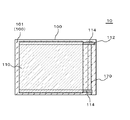
図1は、実施形態に係る発光装置10の構成を示す平面図である。図2は、図1から第2電極130、第2端子132、及び引出配線134を取り除いた図である。図3は、図2から有機層120を取り除いた図である。実施形態に係る発光装置10は、基板100、発光部140、導電膜170、防湿膜101(第1絶縁膜の一例)、第1端子112、及び第2端子132を備えている。発光部140は基板100の第1面に形成されており、第1電極110、第2電極130、及び有機層120を有している。第2電極130は第1電極110の上に位置している。有機層120は第1電極110と第2電極130の間に位置している。導電膜170は基板100の第1面に形成されており、第1電極110の互いに異なる部分すなわち複数の部分に電気的に接続されている。防湿膜101は基板100の第1面に形成されており、導電膜170を覆っている。第1端子112は基板100の第1面に形成されており、導電膜170に接続している。第2端子132は基板100の第1面に形成されており、第2電極130に接続している。以下、詳細に説明する。   FIG. 1 is a plan view showing a configuration of a light emitting device 10 according to the embodiment. FIG. 2 is a diagram in which the second electrode 130, the second terminal 132, and the lead wiring 134 are removed from FIG. 1. FIG. 3 is a diagram in which the organic layer 120 is removed from FIG. The light emitting device 10 according to the embodiment includes a substrate 100, a light emitting unit 140, a conductive film 170, a moisture-proof film 101 (an example of a first insulating film), a first terminal 112, and a second terminal 132. The light emitting unit 140 is formed on the first surface of the substrate 100 and includes the first electrode 110, the second electrode 130, and the organic layer 120. The second electrode 130 is located on the first electrode 110. The organic layer 120 is located between the first electrode 110 and the second electrode 130. The conductive film 170 is formed on the first surface of the substrate 100 and is electrically connected to different portions of the first electrode 110, that is, a plurality of portions. The moisture-proof film 101 is formed on the first surface of the substrate 100 and covers the conductive film 170. The first terminal 112 is formed on the first surface of the substrate 100 and is connected to the conductive film 170. The second terminal 132 is formed on the first surface of the substrate 100 and is connected to the second electrode 130. Details will be described below.

基板100は、例えばガラス基板や樹脂基板などの透光性を有する基板である。基板100は可撓性を有していてもよい。可撓性を有している場合、基板100の厚さは、例えば10μm以上1000μm以下である。基板100は、例えば矩形などの多角形である。基板100が樹脂基板である場合、基板100は、例えばPEN(ポリエチレンナフタレート)、PES(ポリエーテルサルホン)、PET(ポリエチレンテレフタラート)、又はポリイミドを用いて形成されている。   The substrate 100 is a light-transmitting substrate such as a glass substrate or a resin substrate. The substrate 100 may have flexibility. In the case of flexibility, the thickness of the substrate 100 is, for example, not less than 10 μm and not more than 1000 μm. The substrate 100 is, for example, a polygon such as a rectangle. When the substrate 100 is a resin substrate, the substrate 100 is formed using, for example, PEN (polyethylene naphthalate), PES (polyethersulfone), PET (polyethylene terephthalate), or polyimide.

本図に示す例において、基板100は樹脂基板である。このため、水分が基板100を透過することを抑制するために、基板100のうち少なくとも発光部140が形成されている面(好ましくは両面)には、防湿膜101が形成されている。防湿膜101は、例えばSiN膜やSiON膜などの無機膜を有している。防湿膜101は、この無機膜と有機膜とを積層した膜であってもよい。ここで有機膜としては、例えばアクリル系樹脂やエポキシ系樹脂で、紫外線や熱で硬化し、ガスバリア性を有する物を用いることができる。防湿膜101の厚さは、例えば0.1μm以上10μm以下である。 In the example shown in the figure, the substrate 100 is a resin substrate. For this reason, in order to suppress moisture from passing through the substrate 100, the moisture-proof film 101 is formed on at least the surface (preferably both surfaces) of the substrate 100 where the light emitting unit 140 is formed. The moisture-proof film 101 includes an inorganic film such as a SiN x film or a SiON film. The moisture-proof film 101 may be a film in which this inorganic film and an organic film are laminated. Here, as the organic film, for example, an acrylic resin or an epoxy resin that is cured by ultraviolet rays or heat and has a gas barrier property can be used. The thickness of the moisture-proof film 101 is, for example, not less than 0.1 μm and not more than 10 μm.

なお、基板100の平面形状は、例えば矩形などの多角形である。そして上述した第1端子112及び第2端子132は基板100の一辺に沿って配置されている。そして導電膜170は、この一辺に沿って延在している。   The planar shape of the substrate 100 is a polygon such as a rectangle. The first terminal 112 and the second terminal 132 described above are arranged along one side of the substrate 100. The conductive film 170 extends along this one side.

基板100の第1面には発光部140が形成されている。発光部140は、有機EL素子を有している。この有機EL素子は、第1電極110、有機層120、及び第2電極130をこの順に積層させた構成を有している。第1電極110は例えば陽極であり、第2電極130は例えば陰極である。   A light emitting unit 140 is formed on the first surface of the substrate 100. The light emitting unit 140 has an organic EL element. This organic EL element has a configuration in which a first electrode 110, an organic layer 120, and a second electrode 130 are laminated in this order. The first electrode 110 is, for example, an anode, and the second electrode 130 is, for example, a cathode.

第1電極110は、光透過性を有する透明電極である。透明電極の材料は、金属を含む材料、例えば、ITO(Indium Tin Oxide)、IZO(Indium Zinc Oxide)、IWZO(Indium Tungsten Zinc Oxide)、ZnO(Zinc Oxide)等の金属酸化物である。第1電極110の厚さは、例えば10nm以上500nm以下である。第1電極110は、例えばスパッタリング法又は蒸着法を用いて形成される。なお、第1電極110は、カーボンナノチューブ、又はPEDOT/PSSなどの導電性有機材料であってもよく、この場合印刷法で形成されてもよい。   The first electrode 110 is a transparent electrode having optical transparency. The material of the transparent electrode is a material containing a metal, for example, a metal oxide such as ITO (Indium Tin Oxide), IZO (Indium Zinc Oxide), IWZO (Indium Tungsten Zinc Oxide), or ZnO (Zinc Oxide). The thickness of the first electrode 110 is, for example, not less than 10 nm and not more than 500 nm. The first electrode 110 is formed using, for example, a sputtering method or a vapor deposition method. The first electrode 110 may be a carbon nanotube or a conductive organic material such as PEDOT / PSS. In this case, the first electrode 110 may be formed by a printing method.

有機層120は発光層を有している。有機層120は、例えば、正孔注入層、発光層、及び電子注入層をこの順に積層させた構成を有している。正孔注入層と発光層との間には正孔輸送層が形成されていてもよい。また、発光層と電子注入層との間には電子輸送層が形成されていてもよい。有機層120は蒸着法で形成されてもよい。また、有機層120のうち少なくとも一つの層、例えば第1電極110と接触する層は、インクジェット法、印刷法、又はスプレー法などの塗布法によって形成されてもよい。なお、この場合、有機層120の残りの層は、蒸着法によって形成されている。また、有機層120のすべての層が、塗布法を用いて形成されていてもよい。   The organic layer 120 has a light emitting layer. The organic layer 120 has a configuration in which, for example, a hole injection layer, a light emitting layer, and an electron injection layer are stacked in this order. A hole transport layer may be formed between the hole injection layer and the light emitting layer. In addition, an electron transport layer may be formed between the light emitting layer and the electron injection layer. The organic layer 120 may be formed by a vapor deposition method. In addition, at least one layer of the organic layer 120, for example, a layer in contact with the first electrode 110, may be formed by a coating method such as an inkjet method, a printing method, or a spray method. In this case, the remaining layers of the organic layer 120 are formed by vapor deposition. Moreover, all the layers of the organic layer 120 may be formed using the apply | coating method.

第2電極130は、例えば、Al、Au、Ag、Pt、Mg、Sn、Zn、及びInからなる第1群の中から選択される金属、又はこの第1群から選択される金属の合金からなる金属層を含んでいる。この場合、第2電極130は遮光性を有している。第2電極130の厚さは、例えば10nm以上500nm以下である。ただし、第2電極130は、第1電極110の材料として例示した材料を用いて形成されていてもよいし、上述した金属、又は金属合金を極薄膜化したものでも良い。この場合、第2電極130は透明もしくは半透明状態になっている。第2電極130は、例えばスパッタリング法、蒸着法もしくは印刷法を用いて形成される。なお、有機層120は第2電極130よりも広く形成されている。このため、第1電極110と第2電極130は短絡しない。   The second electrode 130 is made of, for example, a metal selected from the first group consisting of Al, Au, Ag, Pt, Mg, Sn, Zn, and In, or an alloy of a metal selected from the first group. Contains a metal layer. In this case, the second electrode 130 has a light shielding property. The thickness of the second electrode 130 is, for example, not less than 10 nm and not more than 500 nm. However, the second electrode 130 may be formed using the material exemplified as the material of the first electrode 110, or may be a thin film made of the above-described metal or metal alloy. In this case, the second electrode 130 is in a transparent or translucent state. The second electrode 130 is formed using, for example, a sputtering method, a vapor deposition method, or a printing method. The organic layer 120 is formed wider than the second electrode 130. For this reason, the 1st electrode 110 and the 2nd electrode 130 do not short-circuit.

発光装置10は、第1端子112を有している。第1端子112は第1電極110に電気的に接続している。本図に示す例において、第1端子112は引出配線114の一端である。   The light emitting device 10 has a first terminal 112. The first terminal 112 is electrically connected to the first electrode 110. In the example shown in the drawing, the first terminal 112 is one end of the lead wiring 114.

詳細には、防湿膜101と第1電極110の間には、引出配線114が形成されている。引出配線114は例えば金属膜、又は金属膜を積層した積層膜である。引出配線114は、例えばMo又はMo合金からなる膜、Al又はAl合金からなる膜、及びMo又はMo合金からなる膜をこの順に積層した構成を有している。引出配線114の一端は第1電極110の外部に延在しており、第1端子112となっている。本図に示す例では、基板100は矩形であり、第1電極110も矩形である。そして引出配線114は、第1電極110の4辺のうち導電膜170と交わる方向に延在している2辺のそれぞれに沿って形成されている。なお、第1端子112は一方の引出配線114にのみ形成されている。第1端子112を有さない引出配線114は、導電膜170を介して第1端子112に接続している。   Specifically, a lead-out wiring 114 is formed between the moisture-proof film 101 and the first electrode 110. The lead wiring 114 is, for example, a metal film or a laminated film in which metal films are laminated. The lead-out wiring 114 has a configuration in which, for example, a film made of Mo or Mo alloy, a film made of Al or Al alloy, and a film made of Mo or Mo alloy are stacked in this order. One end of the lead wiring 114 extends to the outside of the first electrode 110 and serves as a first terminal 112. In the example shown in the figure, the substrate 100 is rectangular, and the first electrode 110 is also rectangular. The lead-out wiring 114 is formed along each of two sides extending in a direction intersecting the conductive film 170 among the four sides of the first electrode 110. The first terminal 112 is formed only on one lead wiring 114. The lead-out wiring 114 that does not have the first terminal 112 is connected to the first terminal 112 through the conductive film 170.

なお、導電膜170に沿う方向において、引出配線134及び第2端子132は、第1の引出配線114と導電膜170の接続点(平面視における交点)と、第2の引出配線114と導電膜170の接続点(平面視における交点)の間に位置している。   Note that in the direction along the conductive film 170, the lead-out wiring 134 and the second terminal 132 are connected to the connection point (intersection in plan view) of the first lead-out wiring 114 and the conductive film 170, and the second lead-out wiring 114 and the conductive film. It is located between 170 connection points (intersection points in plan view).

また、発光装置10は第2端子132を有している。第2端子132は防湿膜101の上に位置しており、また、第2電極130に接続している。本図に示す例において、第2電極130の一部は基板100の縁に向かって第2電極130の本体から飛びだしており、引出配線134となっている。そして、引出配線134の一端が第2端子132となっている。なお、引出配線134は、導電膜170と重なる方向に延在している。このようにして、第1端子112と第2端子132は基板100の同一の辺に沿って配置される。   In addition, the light emitting device 10 has a second terminal 132. The second terminal 132 is located on the moisture-proof film 101 and is connected to the second electrode 130. In the example shown in this drawing, a part of the second electrode 130 protrudes from the main body of the second electrode 130 toward the edge of the substrate 100 and serves as a lead-out wiring 134. One end of the lead wiring 134 serves as the second terminal 132. The lead wiring 134 extends in a direction overlapping the conductive film 170. In this way, the first terminal 112 and the second terminal 132 are disposed along the same side of the substrate 100.

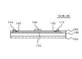
図4は図1のA−A断面図であり、図5は図1のB−B断面図である。図5に示すように、基板100と防湿膜101の間には導電膜170が形成されている。導電膜170は、例えば銀などからなる金属膜と、ITOやIZOなどの透明導電材料からなる膜との積層構造を有していても良いし、金属膜のみで形成されていてもよい。   4 is a cross-sectional view taken along the line AA in FIG. 1, and FIG. 5 is a cross-sectional view taken along the line BB in FIG. As shown in FIG. 5, a conductive film 170 is formed between the substrate 100 and the moisture-proof film 101. The conductive film 170 may have a laminated structure of, for example, a metal film made of silver or the like and a film made of a transparent conductive material such as ITO or IZO, or may be formed of only a metal film.

また、図4及び図5に示すように、引出配線114は防湿膜101の上に形成されている。そして防湿膜101のうち引出配線114と導電膜170の双方と重なる部分には、開口103が形成されている。引出配線114の一部は、開口103の内部に入り込み、導電膜170に接続している。このようにして、引出配線114は導電膜170に接続している。   Further, as shown in FIGS. 4 and 5, the lead-out wiring 114 is formed on the moisture-proof film 101. An opening 103 is formed in a portion of the moisture-proof film 101 that overlaps both the lead-out wiring 114 and the conductive film 170. A part of the lead wiring 114 enters the opening 103 and is connected to the conductive film 170. In this way, the lead wiring 114 is connected to the conductive film 170.

なお、発光装置10は、さらに封止部材を有していてもよい。封止部材は、例えばガラス、樹脂又は金属箔を用いて形成されており、基板100と同様の多角形や円形である。また封止部材の中央に凹部を設けた形状を有してもよい。そして封止部材の縁は接着材で基板100に固定されている。これにより、封止部材と基板100で囲まれた空間は封止される。そして発光部140は、この封止された空間の中に位置している。なお、封止部材はALD法で形成された膜又はCVD法で形成された膜であってもよい。   The light emitting device 10 may further include a sealing member. The sealing member is formed using, for example, glass, resin, or metal foil, and has the same polygon or circle as the substrate 100. Moreover, you may have the shape which provided the recessed part in the center of the sealing member. The edge of the sealing member is fixed to the substrate 100 with an adhesive. Thereby, the space surrounded by the sealing member and the substrate 100 is sealed. And the light emission part 140 is located in this sealed space. The sealing member may be a film formed by the ALD method or a film formed by the CVD method.

また、発光装置10は、さらに乾燥剤を有していてもよい。乾燥剤は、例えば封止部材によって封止された空間内、例えば封止部材のうち基板100に対向する面に配置されている。   The light emitting device 10 may further have a desiccant. The desiccant is disposed, for example, in the space sealed by the sealing member, for example, on the surface of the sealing member that faces the substrate 100.

次に、発光装置10の製造方法について説明する。まず、防湿膜101を形成する前の基板100を準備する。次いで、基板100の第1面上に、導電膜170となる導電膜を形成する。次いで、この導電膜上にレジストパターンを形成し、このレジストパターンを用いて導電膜をエッチングする。これにより、導電膜170が形成される。なお、導電膜170は、マスクを用いたスパッタリング法や、インクジェット法などの塗布法を用いて形成されてもよい。   Next, a method for manufacturing the light emitting device 10 will be described. First, the substrate 100 before forming the moisture-proof film 101 is prepared. Next, a conductive film to be the conductive film 170 is formed over the first surface of the substrate 100. Next, a resist pattern is formed on the conductive film, and the conductive film is etched using the resist pattern. Thereby, the conductive film 170 is formed. Note that the conductive film 170 may be formed by a sputtering method using a mask or a coating method such as an inkjet method.

次いで、基板100に防湿膜101を形成する。防湿膜101は、例えばCVD法やスパッタリング法を用いて形成される。次いで、防湿膜101上にレジストパターンを形成し、このレジストパターンをマスクとして防湿膜101を除去する。これにより、防湿膜101には開口103が形成される。なお、開口103の形成には、RIE(Reactive Ion Etching)などのドライエッチング、またはウェットエッチングが用いられる。もしくは、防湿膜101は開口部を設けたマスクを用いた真空成膜法や、塗布型材料を用いた印刷法によってパターニングされてもよい。   Next, a moisture-proof film 101 is formed on the substrate 100. The moisture-proof film 101 is formed using, for example, a CVD method or a sputtering method. Next, a resist pattern is formed on the moisture-proof film 101, and the moisture-proof film 101 is removed using this resist pattern as a mask. Thereby, an opening 103 is formed in the moisture-proof film 101. The opening 103 is formed by dry etching such as RIE (Reactive Ion Etching) or wet etching. Alternatively, the moisture-proof film 101 may be patterned by a vacuum film forming method using a mask provided with an opening or a printing method using a coating type material.

次いで、防湿膜101上に、引出配線114となる導電膜を、例えばスパッタリング法を用いて形成する。次いで、この導電膜を、例えばフォトリソグラフィー法を利用して所定のパターンにする。これにより、引出配線114及び第1端子112が形成される。この工程において、引出配線114の一部は開口103の中に位置するため、引出配線114は導電膜170に接続する。   Next, a conductive film to be the lead wiring 114 is formed on the moisture-proof film 101 by using, for example, a sputtering method. Next, the conductive film is formed into a predetermined pattern using, for example, a photolithography method. Thereby, the lead wiring 114 and the first terminal 112 are formed. In this process, since a part of the lead wiring 114 is located in the opening 103, the lead wiring 114 is connected to the conductive film 170.

次いで、防湿膜101上及び引出配線114上に、第1電極110となる導電膜を、例えばスパッタリング法を用いて形成する。次いで、この導電膜を、例えばフォトリソグラフィー法を利用して所定のパターンにする。これにより、第1電極110が形成される。また第1電極110は、スパッタリング法で成膜する際に、開口部を設けたマスクを用いることで所定のパターンに形成してもよいし、塗布型材料を用いた印刷法によって形成してもよい。   Next, a conductive film to be the first electrode 110 is formed on the moisture-proof film 101 and the lead wiring 114 by using, for example, a sputtering method. Next, the conductive film is formed into a predetermined pattern using, for example, a photolithography method. Thereby, the first electrode 110 is formed. The first electrode 110 may be formed in a predetermined pattern by using a mask provided with an opening when forming a film by a sputtering method, or may be formed by a printing method using a coating type material. Good.

次いで、有機層120及び第2電極130をこの順に形成する。有機層120が蒸着法で形成される層を含む場合、この層は、例えばマスクを用いるなどして所定のパターンに形成される。第2電極130も、例えばマスクを用いるなどして所定のパターンに形成される。その後、封止部材(図示せず)を用いて発光部140を封止する。   Next, the organic layer 120 and the second electrode 130 are formed in this order. When the organic layer 120 includes a layer formed by an evaporation method, this layer is formed in a predetermined pattern using, for example, a mask. The second electrode 130 is also formed in a predetermined pattern using, for example, a mask. Thereafter, the light emitting unit 140 is sealed using a sealing member (not shown).

なお、上述した例において、引出配線114は第1電極110が形成される前に形成されているが、第1電極110が形成された後に形成されてもよい。この場合、引出配線114のうち第1電極110と重なる部分は、第1電極110の上に位置する。   In the above-described example, the lead-out wiring 114 is formed before the first electrode 110 is formed, but may be formed after the first electrode 110 is formed. In this case, a portion of the lead-out wiring 114 that overlaps the first electrode 110 is located on the first electrode 110.

また、引出配線114を設けずに、導電膜170を、本実施形態における導電膜170と引出配線114を合わせたパターンにしてもよい。この場合、導電膜170は基板100の3辺に沿ったパターンになる。そして、導電膜170のうち引出配線114に相当するラインの上には防湿膜101は形成されず、直接第1電極110に接続する。   Further, the conductive film 170 may be a pattern in which the conductive film 170 and the lead wiring 114 in this embodiment are combined without providing the lead wiring 114. In this case, the conductive film 170 has a pattern along the three sides of the substrate 100. The moisture-proof film 101 is not formed on the line corresponding to the lead wiring 114 in the conductive film 170, and is directly connected to the first electrode 110.

以上、本実施形態によれば、導電膜170は第1電極110のうち互いに異なる部分に電気的に接続している。このため、導電膜170を第1端子112に接続することにより、第1端子112から第1電極110のうち互いに異なる部分に給電することができる。従って、第1端子112の数を増やすことなく、第1電極110のうち給電される領域を増やすことができる。また、導電膜170は絶縁性の防湿膜101によって覆われている。このため、導電膜170を設けても、第1電極110と第2電極130が短絡する可能性はない。   As described above, according to the present embodiment, the conductive film 170 is electrically connected to different portions of the first electrode 110. For this reason, by connecting the conductive film 170 to the first terminal 112, power can be supplied from the first terminal 112 to different portions of the first electrode 110. Therefore, it is possible to increase the power supply area of the first electrode 110 without increasing the number of the first terminals 112. The conductive film 170 is covered with an insulating moisture-proof film 101. For this reason, even if the conductive film 170 is provided, there is no possibility that the first electrode 110 and the second electrode 130 are short-circuited.

また本実施形態では、防湿膜101と基板100の間に導電膜170を設けている。従って、導電膜170を覆う絶縁膜を新たに設ける必要がない。従って、発光装置10の製造コストが増加することを抑制できる。   In this embodiment, a conductive film 170 is provided between the moisture-proof film 101 and the substrate 100. Therefore, it is not necessary to newly provide an insulating film that covers the conductive film 170. Therefore, an increase in the manufacturing cost of the light emitting device 10 can be suppressed.

また、第2端子132と第1端子112は、基板100の同一の辺に沿って配置されている。このため、第1端子112及び第2端子132にリード端子などの導電部材を接続するときの労力は少なくなる。特に本実施形態では、第2端子132は2つの引出配線114の間に位置している。従って、第1端子112と第2端子132を近づけることができるため、上記した労力はさらに少なくなる。また、FPC(Flexible Printed Circuits)と接続する必要がある場合にも、小面積のFPCを使用することが可能となり、発光装置10の製造コスト増加を抑制できる。   The second terminal 132 and the first terminal 112 are arranged along the same side of the substrate 100. For this reason, labor when connecting a conductive member such as a lead terminal to the first terminal 112 and the second terminal 132 is reduced. In particular, in the present embodiment, the second terminal 132 is located between the two lead wires 114. Therefore, since the first terminal 112 and the second terminal 132 can be brought closer to each other, the above-described labor is further reduced. Further, even when it is necessary to connect to an FPC (Flexible Printed Circuits), it is possible to use an FPC with a small area, and an increase in manufacturing cost of the light emitting device 10 can be suppressed.

(変形例1)
図6は、変形例1に係る発光装置10の構成を示す平面図であり、実施形態における図3に対応している。図7は図6のA−A断面図を示している。ただし説明のため、図7には有機層120、及び第2電極130も示している。
(Modification 1)
FIG. 6 is a plan view showing a configuration of the light emitting device 10 according to the first modification, and corresponds to FIG. 3 in the embodiment. FIG. 7 shows a cross-sectional view taken along the line AA of FIG. However, for the sake of explanation, FIG. 7 also shows the organic layer 120 and the second electrode 130.

本変形例に係る発光装置10は、複数の補助配線160を備えている点を除いて、実施形態に係る発光装置10と同様の構成である。補助配線160は第1電極110の下に形成されている。詳細には、複数の補助配線160は、2つの引出配線114の間を互いに平行に延在している。そして、補助配線160は、引出配線114と同一工程で形成されており、また、引出配線114と一体になっている。このため、補助配線160の層構造は、引出配線114の層構造と同一である。   The light emitting device 10 according to this modification has the same configuration as that of the light emitting device 10 according to the embodiment, except that a plurality of auxiliary wirings 160 are provided. The auxiliary wiring 160 is formed under the first electrode 110. Specifically, the plurality of auxiliary wirings 160 extend in parallel between the two lead wirings 114. The auxiliary wiring 160 is formed in the same process as the extraction wiring 114 and is integrated with the extraction wiring 114. For this reason, the layer structure of the auxiliary wiring 160 is the same as the layer structure of the lead-out wiring 114.

なお、本変形例によっても、引出配線114及び補助配線160は、第1電極110が形成された後に形成されてもよい。この場合、引出配線114のうち第1電極110と重なる部分、及び補助配線160は、第1電極110の上に位置する。   Note that, also in this modification, the lead-out wiring 114 and the auxiliary wiring 160 may be formed after the first electrode 110 is formed. In this case, a portion of the extraction wiring 114 that overlaps the first electrode 110 and the auxiliary wiring 160 are located on the first electrode 110.

本変形例によっても、実施形態と同様に、第1端子112の数を増やすことなく、第1電極110のうち給電される領域を増やすことができる。また、導電膜170を設けても、第1電極110と第2電極130が短絡する可能性は増加しない。また、第1端子112及び第2端子132にリード端子などの導電部材を接続するときの労力は少なくなる。さらに、FPC(Flexible Printed Circuits)と接続する際にも、小面積のFPCを使用することが可能となり、発光装置10の製造コスト増加を抑制できる。   Also according to the present modification, similarly to the embodiment, it is possible to increase the power supply area of the first electrode 110 without increasing the number of the first terminals 112. Further, even if the conductive film 170 is provided, the possibility that the first electrode 110 and the second electrode 130 are short-circuited does not increase. Further, labor for connecting a conductive member such as a lead terminal to the first terminal 112 and the second terminal 132 is reduced. Furthermore, when connecting with FPC (Flexible Printed Circuits), it becomes possible to use FPC with a small area, and an increase in manufacturing cost of the light emitting device 10 can be suppressed.

また、第1電極110上に補助配線160を設けているため、第1電極110の見かけ上の抵抗を少なくすることができる。従って、発光装置10の輝度の面内分布を小さくすることができる。   Further, since the auxiliary wiring 160 is provided on the first electrode 110, the apparent resistance of the first electrode 110 can be reduced. Therefore, the in-plane distribution of luminance of the light emitting device 10 can be reduced.

(変形例2)
図8は、変形例2に係る発光装置10の平面図である。図9は図8のA−A断面図であり、図10は図8のB−B断面図である。本変形例に係る発光装置10は、以下の点を除いて、実施形態又は変形例1に係る発光装置10と同様の構成である。
(Modification 2)
FIG. 8 is a plan view of the light emitting device 10 according to the second modification. 9 is a cross-sectional view taken along the line AA in FIG. 8, and FIG. 10 is a cross-sectional view taken along the line BB in FIG. The light emitting device 10 according to this modification has the same configuration as that of the light emitting device 10 according to the embodiment or modification 1 except for the following points.

まず、基板100はガラス基板である。このため、第1電極110及び引出配線114と基板100の間には、防湿膜101は形成されていない。   First, the substrate 100 is a glass substrate. Therefore, the moisture-proof film 101 is not formed between the first electrode 110 and the lead wiring 114 and the substrate 100.

また、第1電極110の縁は、第2絶縁膜150によって覆われている。第2絶縁膜150は例えばポリイミドなどの感光性の樹脂材料によって形成されており、第1電極110のうち発光部140の発光領域となる部分を囲んでいる。第2絶縁膜150を設けることにより、第1電極110の縁において第1電極110と第2電極130が短絡することを抑制できる。   The edge of the first electrode 110 is covered with the second insulating film 150. The second insulating film 150 is made of, for example, a photosensitive resin material such as polyimide, and surrounds a portion of the first electrode 110 that becomes a light emitting region of the light emitting unit 140. By providing the second insulating film 150, it is possible to prevent the first electrode 110 and the second electrode 130 from being short-circuited at the edge of the first electrode 110.

また、導電膜170は第1絶縁膜152によって覆われている。第1絶縁膜152は、例えば感光性の樹脂材料によって形成されている。また、第1絶縁膜152は導電膜170と重なる領域にのみ形成されている。第1絶縁膜152は、導電膜170が形成された後、引出配線114が形成される前に形成される。   The conductive film 170 is covered with the first insulating film 152. The first insulating film 152 is made of, for example, a photosensitive resin material. Further, the first insulating film 152 is formed only in a region overlapping with the conductive film 170. The first insulating film 152 is formed after the conductive film 170 is formed and before the extraction wiring 114 is formed.

本変形例によっても、実施形態と同様に、第1端子112の数を増やすことなく、第1電極110のうち給電される領域を増やすことができる。また、導電膜170を設けても、第1電極110と第2電極130が短絡する可能性は増加しない。また、第1端子112及び第2端子132にリード端子などの導電部材を接続するときの労力は少なくなる。さらに、FPC(Flexible Printed Circuits)と接続する際にも、小面積のFPCを使用することが可能となり、発光装置10の製造コスト増加を抑制できる。   Also according to the present modification, similarly to the embodiment, it is possible to increase the power supply area of the first electrode 110 without increasing the number of the first terminals 112. Further, even if the conductive film 170 is provided, the possibility that the first electrode 110 and the second electrode 130 are short-circuited does not increase. Further, labor for connecting a conductive member such as a lead terminal to the first terminal 112 and the second terminal 132 is reduced. Furthermore, when connecting with FPC (Flexible Printed Circuits), it becomes possible to use FPC with a small area, and an increase in manufacturing cost of the light emitting device 10 can be suppressed.

以上、図面を参照して実施形態及び実施例について述べたが、これらは本発明の例示であり、上記以外の様々な構成を採用することもできる。   As mentioned above, although embodiment and the Example were described with reference to drawings, these are illustrations of this invention and can also employ | adopt various structures other than the above.

10 発光装置
100 基板
101 防湿膜
103 開口
110 第1電極
112 第1端子
120 有機層
130 第2電極
132 第2端子
140 発光部
150 第2絶縁膜
152 第1絶縁膜
160 補助配線
170 導電膜
DESCRIPTION OF SYMBOLS 10 Light-emitting device 100 Substrate 101 Moisture-proof film 103 Opening 110 1st electrode 112 1st terminal 120 Organic layer 130 2nd electrode 132 2nd terminal 140 Light-emitting part 150 2nd insulating film 152 1st insulating film 160 Auxiliary wiring 170 Conductive film

Claims (6)

基板と、
前記基板の第1面に形成され、第1電極、前記第1電極の上に位置する第2電極、及び前記第1電極と前記第2電極の間に位置する有機層を有する発光部と、
前記基板の前記第1面に形成され、前記第1電極の複数の部分に電気的に接続されている導電膜と、
前記基板の前記第1面に形成され、前記導電膜を覆う第1絶縁膜と、
前記基板の前記第1面に形成され、前記導電膜に接続する第1端子と、
前記基板の前記第1面に形成され、前記第2電極に接続する第2端子と、
を備える発光装置。
A substrate,
A light-emitting unit formed on the first surface of the substrate and having a first electrode, a second electrode located on the first electrode, and an organic layer located between the first electrode and the second electrode;
A conductive film formed on the first surface of the substrate and electrically connected to a plurality of portions of the first electrode;
A first insulating film formed on the first surface of the substrate and covering the conductive film;
A first terminal formed on the first surface of the substrate and connected to the conductive film;
A second terminal formed on the first surface of the substrate and connected to the second electrode;
A light emitting device comprising:
請求項1に記載の発光装置において、
前記基板は多角形であり、
前記導電膜は前記多角形の一辺に沿って形成されており、
前記第1端子及び前記第2端子は、前記一辺に沿う位置に配置されており、かつ前記第1絶縁膜の上に位置している発光装置。
The light-emitting device according to claim 1.
The substrate is polygonal;
The conductive film is formed along one side of the polygon;
The light emitting device, wherein the first terminal and the second terminal are disposed at a position along the one side and are located on the first insulating film.
請求項2に記載の発光装置において、
前記一辺に沿う方向において、前記第2端子は、前記導電膜と前記第1電極が電気的に接続している複数の接続点の間に位置している発光装置。
The light-emitting device according to claim 2.
In the direction along the one side, the second terminal is located between a plurality of connection points at which the conductive film and the first electrode are electrically connected.
請求項1〜3のいずれか一項に記載の発光装置において、
前記基板は樹脂基板であり、
前記第1絶縁膜は、前記基板の前記第1面に形成された防湿膜であり、
前記第1端子は、前記防湿膜の上に形成されており、かつ前記防湿膜に形成された開口を介して前記第1電極に電気的に接続している発光装置。
In the light-emitting device as described in any one of Claims 1-3,
The substrate is a resin substrate;
The first insulating film is a moisture-proof film formed on the first surface of the substrate;
The light emitting device, wherein the first terminal is formed on the moisture-proof film and is electrically connected to the first electrode through an opening formed in the moisture-proof film.
請求項4に記載の発光装置において、
前記防湿膜は無機膜を有している発光装置。
The light-emitting device according to claim 4.
The moisture-proof film is a light emitting device having an inorganic film.
請求項1〜3のいずれか一項に記載の発光装置において、
前記第1絶縁膜は樹脂膜である発光装置。
In the light-emitting device as described in any one of Claims 1-3,
The light emitting device wherein the first insulating film is a resin film.
JP2014239112A 2014-11-26 2014-11-26 Light emitting device Pending JP2016100314A (en)

Priority Applications (1)

Application Number Priority Date Filing Date Title
JP2014239112A JP2016100314A (en) 2014-11-26 2014-11-26 Light emitting device

Applications Claiming Priority (1)

Application Number Priority Date Filing Date Title
JP2014239112A JP2016100314A (en) 2014-11-26 2014-11-26 Light emitting device

Publications (1)

Publication Number Publication Date
JP2016100314A true JP2016100314A (en) 2016-05-30

Family

ID=56077371

Family Applications (1)

Application Number Title Priority Date Filing Date
JP2014239112A Pending JP2016100314A (en) 2014-11-26 2014-11-26 Light emitting device

Country Status (1)

Country Link
JP (1) JP2016100314A (en)

Citations (8)

* Cited by examiner, † Cited by third party
Publication number Priority date Publication date Assignee Title
JP2004319484A (en) * 2003-04-11 2004-11-11 Eastman Kodak Co Method and device for forming transparent moisture-proof layer, and moisture-proof oled device
JP2007156058A (en) * 2005-12-05 2007-06-21 Seiko Epson Corp Light emitting device and electronic apparatus
JP2009205897A (en) * 2008-02-27 2009-09-10 Rohm Co Ltd Organic light-emitting device and manufacturing method of the same
JP2009211828A (en) * 2008-02-29 2009-09-17 Rohm Co Ltd Illuminating device and method of manufacturing illuminating device
WO2010150648A1 (en) * 2009-06-25 2010-12-29 コニカミノルタホールディングス株式会社 Organic electronics panel and method for producing the same
JP2012146686A (en) * 2000-02-22 2012-08-02 Semiconductor Energy Lab Co Ltd El display device
WO2012133716A1 (en) * 2011-03-29 2012-10-04 Necライティング株式会社 Organic el light emitting device, manufacturing method therefor, and organic el illumination device
WO2013118508A1 (en) * 2012-02-07 2013-08-15 パナソニック株式会社 Composite substrate, method for manufacturing same, and organic electroluminescence device

Patent Citations (8)

* Cited by examiner, † Cited by third party
Publication number Priority date Publication date Assignee Title
JP2012146686A (en) * 2000-02-22 2012-08-02 Semiconductor Energy Lab Co Ltd El display device
JP2004319484A (en) * 2003-04-11 2004-11-11 Eastman Kodak Co Method and device for forming transparent moisture-proof layer, and moisture-proof oled device
JP2007156058A (en) * 2005-12-05 2007-06-21 Seiko Epson Corp Light emitting device and electronic apparatus
JP2009205897A (en) * 2008-02-27 2009-09-10 Rohm Co Ltd Organic light-emitting device and manufacturing method of the same
JP2009211828A (en) * 2008-02-29 2009-09-17 Rohm Co Ltd Illuminating device and method of manufacturing illuminating device
WO2010150648A1 (en) * 2009-06-25 2010-12-29 コニカミノルタホールディングス株式会社 Organic electronics panel and method for producing the same
WO2012133716A1 (en) * 2011-03-29 2012-10-04 Necライティング株式会社 Organic el light emitting device, manufacturing method therefor, and organic el illumination device
WO2013118508A1 (en) * 2012-02-07 2013-08-15 パナソニック株式会社 Composite substrate, method for manufacturing same, and organic electroluminescence device

Similar Documents

Publication Publication Date Title
US20240099050A1 (en) Light-emitting device
JP6617024B2 (en) Light emitting device
JP2016149223A (en) Light-emitting device
JPWO2016151820A1 (en) Light emitting device
JP6555911B2 (en) Light emitting device
JP2016100314A (en) Light emitting device
JP2016072283A (en) Light emission device
JP6496138B2 (en) Light emitting device
WO2017183118A1 (en) Light-emitting device
JPWO2017163331A1 (en) LIGHT EMITTING DEVICE, ELECTRONIC DEVICE, AND METHOD FOR MANUFACTURING LIGHT EMITTING DEVICE
JP6700013B2 (en) Light emitting device
JP6580336B2 (en) Light emitting device
JP2016095990A (en) Light emission device
JP6294071B2 (en) Light emitting device
WO2017154207A1 (en) Light-emitting device
JP2021193687A (en) Light-emitting device
JP2014203526A (en) Junction structure and light-emitting device
JP2019201004A (en) Light-emitting device
JP2020013797A (en) Light-emitting device manufacturing method
JP2019165026A (en) Light-emitting device
JP2017162765A (en) Light-emitting device
WO2016129114A1 (en) Light-emitting device and method for producing light-emitting device
JP2016143529A (en) Light emission device
WO2016151819A1 (en) Light-emitting device
WO2016059714A1 (en) Light emitting device

Legal Events

Date Code Title Description
A621 Written request for application examination

Free format text: JAPANESE INTERMEDIATE CODE: A621

Effective date: 20171005

A977 Report on retrieval

Free format text: JAPANESE INTERMEDIATE CODE: A971007

Effective date: 20180810

A131 Notification of reasons for refusal

Free format text: JAPANESE INTERMEDIATE CODE: A131

Effective date: 20181002

A02 Decision of refusal

Free format text: JAPANESE INTERMEDIATE CODE: A02

Effective date: 20190402