JP2015204301A - Semiconductor device and method of manufacturing the same - Google Patents
Semiconductor device and method of manufacturing the same Download PDFInfo
- Publication number
- JP2015204301A JP2015204301A JP2014081239A JP2014081239A JP2015204301A JP 2015204301 A JP2015204301 A JP 2015204301A JP 2014081239 A JP2014081239 A JP 2014081239A JP 2014081239 A JP2014081239 A JP 2014081239A JP 2015204301 A JP2015204301 A JP 2015204301A
- Authority
- JP
- Japan
- Prior art keywords
- electrode film
- type silicon
- semiconductor device
- silicon substrate
- layer
- Prior art date
- Legal status (The legal status is an assumption and is not a legal conclusion. Google has not performed a legal analysis and makes no representation as to the accuracy of the status listed.)
- Pending
Links
- 239000004065 semiconductor Substances 0.000 title claims abstract description 52
- 238000004519 manufacturing process Methods 0.000 title claims abstract description 18
- XUIMIQQOPSSXEZ-UHFFFAOYSA-N Silicon Chemical compound [Si] XUIMIQQOPSSXEZ-UHFFFAOYSA-N 0.000 claims abstract description 64
- 229910052710 silicon Inorganic materials 0.000 claims abstract description 64
- 239000010703 silicon Substances 0.000 claims abstract description 64
- 239000000758 substrate Substances 0.000 claims abstract description 36
- 229910008332 Si-Ti Inorganic materials 0.000 claims abstract description 22
- 229910006749 Si—Ti Inorganic materials 0.000 claims abstract description 22
- 239000010936 titanium Substances 0.000 claims abstract description 21
- 229910018125 Al-Si Inorganic materials 0.000 claims abstract description 17
- 229910018520 Al—Si Inorganic materials 0.000 claims abstract description 17
- RTAQQCXQSZGOHL-UHFFFAOYSA-N Titanium Chemical compound [Ti] RTAQQCXQSZGOHL-UHFFFAOYSA-N 0.000 claims abstract description 13
- 229910052719 titanium Inorganic materials 0.000 claims abstract description 13
- 230000001681 protective effect Effects 0.000 claims description 13
- 229910021341 titanium silicide Inorganic materials 0.000 claims description 11
- 238000010438 heat treatment Methods 0.000 claims description 9
- 230000006866 deterioration Effects 0.000 abstract description 4
- 229910000789 Aluminium-silicon alloy Inorganic materials 0.000 abstract description 3
- 238000000034 method Methods 0.000 description 22
- 229910000679 solder Inorganic materials 0.000 description 9
- 238000010586 diagram Methods 0.000 description 6
- 230000015572 biosynthetic process Effects 0.000 description 5
- 230000001771 impaired effect Effects 0.000 description 5
- 238000009792 diffusion process Methods 0.000 description 4
- 229910045601 alloy Inorganic materials 0.000 description 3
- 239000000956 alloy Substances 0.000 description 3
- 230000000694 effects Effects 0.000 description 3
- 230000004888 barrier function Effects 0.000 description 2
- 239000012528 membrane Substances 0.000 description 2
- 229910052751 metal Inorganic materials 0.000 description 2
- 239000002184 metal Substances 0.000 description 2
- 229910000838 Al alloy Inorganic materials 0.000 description 1
- 230000007547 defect Effects 0.000 description 1
- 230000032798 delamination Effects 0.000 description 1
- 230000002349 favourable effect Effects 0.000 description 1
- 230000002427 irreversible effect Effects 0.000 description 1
- 238000000926 separation method Methods 0.000 description 1
- 230000001629 suppression Effects 0.000 description 1
Images


Classifications
-
- H—ELECTRICITY
- H01—ELECTRIC ELEMENTS
- H01L—SEMICONDUCTOR DEVICES NOT COVERED BY CLASS H10
- H01L29/00—Semiconductor devices adapted for rectifying, amplifying, oscillating or switching, or capacitors or resistors with at least one potential-jump barrier or surface barrier, e.g. PN junction depletion layer or carrier concentration layer; Details of semiconductor bodies or of electrodes thereof ; Multistep manufacturing processes therefor
- H01L29/40—Electrodes ; Multistep manufacturing processes therefor
- H01L29/43—Electrodes ; Multistep manufacturing processes therefor characterised by the materials of which they are formed
- H01L29/45—Ohmic electrodes
- H01L29/456—Ohmic electrodes on silicon
-
- H—ELECTRICITY
- H01—ELECTRIC ELEMENTS
- H01L—SEMICONDUCTOR DEVICES NOT COVERED BY CLASS H10
- H01L21/00—Processes or apparatus adapted for the manufacture or treatment of semiconductor or solid state devices or of parts thereof
- H01L21/02—Manufacture or treatment of semiconductor devices or of parts thereof
- H01L21/04—Manufacture or treatment of semiconductor devices or of parts thereof the devices having at least one potential-jump barrier or surface barrier, e.g. PN junction, depletion layer or carrier concentration layer
- H01L21/0445—Manufacture or treatment of semiconductor devices or of parts thereof the devices having at least one potential-jump barrier or surface barrier, e.g. PN junction, depletion layer or carrier concentration layer the devices having semiconductor bodies comprising crystalline silicon carbide
- H01L21/048—Making electrodes
- H01L21/0485—Ohmic electrodes
-
- H—ELECTRICITY
- H01—ELECTRIC ELEMENTS
- H01L—SEMICONDUCTOR DEVICES NOT COVERED BY CLASS H10
- H01L21/00—Processes or apparatus adapted for the manufacture or treatment of semiconductor or solid state devices or of parts thereof
- H01L21/02—Manufacture or treatment of semiconductor devices or of parts thereof
- H01L21/04—Manufacture or treatment of semiconductor devices or of parts thereof the devices having at least one potential-jump barrier or surface barrier, e.g. PN junction, depletion layer or carrier concentration layer
- H01L21/18—Manufacture or treatment of semiconductor devices or of parts thereof the devices having at least one potential-jump barrier or surface barrier, e.g. PN junction, depletion layer or carrier concentration layer the devices having semiconductor bodies comprising elements of Group IV of the Periodic System or AIIIBV compounds with or without impurities, e.g. doping materials
- H01L21/28—Manufacture of electrodes on semiconductor bodies using processes or apparatus not provided for in groups H01L21/20 - H01L21/268
- H01L21/283—Deposition of conductive or insulating materials for electrodes conducting electric current
- H01L21/285—Deposition of conductive or insulating materials for electrodes conducting electric current from a gas or vapour, e.g. condensation
- H01L21/28506—Deposition of conductive or insulating materials for electrodes conducting electric current from a gas or vapour, e.g. condensation of conductive layers
- H01L21/28512—Deposition of conductive or insulating materials for electrodes conducting electric current from a gas or vapour, e.g. condensation of conductive layers on semiconductor bodies comprising elements of Group IV of the Periodic System
- H01L21/28568—Deposition of conductive or insulating materials for electrodes conducting electric current from a gas or vapour, e.g. condensation of conductive layers on semiconductor bodies comprising elements of Group IV of the Periodic System the conductive layers comprising transition metals
-
- H—ELECTRICITY
- H01—ELECTRIC ELEMENTS
- H01L—SEMICONDUCTOR DEVICES NOT COVERED BY CLASS H10
- H01L29/00—Semiconductor devices adapted for rectifying, amplifying, oscillating or switching, or capacitors or resistors with at least one potential-jump barrier or surface barrier, e.g. PN junction depletion layer or carrier concentration layer; Details of semiconductor bodies or of electrodes thereof ; Multistep manufacturing processes therefor
- H01L29/40—Electrodes ; Multistep manufacturing processes therefor
- H01L29/41—Electrodes ; Multistep manufacturing processes therefor characterised by their shape, relative sizes or dispositions
- H01L29/417—Electrodes ; Multistep manufacturing processes therefor characterised by their shape, relative sizes or dispositions carrying the current to be rectified, amplified or switched
- H01L29/41708—Emitter or collector electrodes for bipolar transistors
-
- H—ELECTRICITY
- H01—ELECTRIC ELEMENTS
- H01L—SEMICONDUCTOR DEVICES NOT COVERED BY CLASS H10
- H01L29/00—Semiconductor devices adapted for rectifying, amplifying, oscillating or switching, or capacitors or resistors with at least one potential-jump barrier or surface barrier, e.g. PN junction depletion layer or carrier concentration layer; Details of semiconductor bodies or of electrodes thereof ; Multistep manufacturing processes therefor
- H01L29/66—Types of semiconductor device ; Multistep manufacturing processes therefor
- H01L29/68—Types of semiconductor device ; Multistep manufacturing processes therefor controllable by only the electric current supplied, or only the electric potential applied, to an electrode which does not carry the current to be rectified, amplified or switched
- H01L29/70—Bipolar devices
- H01L29/72—Transistor-type devices, i.e. able to continuously respond to applied control signals
- H01L29/73—Bipolar junction transistors
- H01L29/732—Vertical transistors
-
- H—ELECTRICITY
- H01—ELECTRIC ELEMENTS
- H01L—SEMICONDUCTOR DEVICES NOT COVERED BY CLASS H10
- H01L29/00—Semiconductor devices adapted for rectifying, amplifying, oscillating or switching, or capacitors or resistors with at least one potential-jump barrier or surface barrier, e.g. PN junction depletion layer or carrier concentration layer; Details of semiconductor bodies or of electrodes thereof ; Multistep manufacturing processes therefor
- H01L29/66—Types of semiconductor device ; Multistep manufacturing processes therefor
- H01L29/86—Types of semiconductor device ; Multistep manufacturing processes therefor controllable only by variation of the electric current supplied, or only the electric potential applied, to one or more of the electrodes carrying the current to be rectified, amplified, oscillated or switched
- H01L29/861—Diodes
- H01L29/8611—Planar PN junction diodes
Abstract
Description
本発明は、半導体装置および半導体装置の製造方法に関する。 The present invention relates to a semiconductor device and a method for manufacturing the semiconductor device.
従来、例えば、下記の特許文献1、2に開示されているように、シリコン基板に多層電極膜を設けた半導体装置が知られている。例えば特許文献1の図6を参照すると、シリコン基板の表面に、Tiなどのバリアメタルと、AlSi合金などのAl合金電極と、Ni電極と、Au電極とが積層された構造が記載されている。
Conventionally, for example, as disclosed in
N型シリコン(Si)にチタン(Ti)からなる電極を設けてSi−Ti接合を形成すると、良好なオーミックコンタクト性が得られる。強固なSi−Ti接合を得るために、理想的には、700℃程度の高温プロセスを用いチタンシリサイドなどの反応層を得ることが好ましい。しかし、このような高温プロセスを行うと、半導体基板に既に形成された素子構造部、電極膜、および保護膜の機能が損なわれるという問題がある。これに対し、そのような高温プロセスを行わずにチタンシリサイドなどの反応層が形成されていないSi−Ti接合を用いることも考えられる。しかしながら、その場合には、チタン電極に更に他の電極膜を重ねて多層電極膜を形成した後に、この多層電極膜に熱処理工程(200度以上)を加えると、多層電極膜の応力によりSi−Ti界面剥離が発生するという問題があった。 If an Si-Ti junction is formed by providing an electrode made of titanium (Ti) on N-type silicon (Si), good ohmic contact properties can be obtained. In order to obtain a strong Si-Ti junction, ideally, it is preferable to obtain a reaction layer such as titanium silicide using a high temperature process of about 700 ° C. However, when such a high temperature process is performed, there is a problem that the functions of the element structure, the electrode film, and the protective film already formed on the semiconductor substrate are impaired. On the other hand, it is conceivable to use a Si—Ti junction in which a reaction layer such as titanium silicide is not formed without performing such a high temperature process. However, in that case, if another electrode film is further stacked on the titanium electrode to form a multilayer electrode film, and then a heat treatment step (200 ° C. or more) is applied to the multilayer electrode film, Si— There was a problem that Ti interface peeling occurred.
本発明は、上述のような課題を解決するためになされたもので、良好な電気特性を得つつ、シリコン基板に形成された保護膜などの機能が損なわれるのを抑制し、Si−Ti面の剥離を抑制することもできる半導体装置および半導体装置の製造方法を提供することを目的とする。 The present invention has been made in order to solve the above-described problems, and while suppressing good functions such as a protective film formed on a silicon substrate while obtaining good electrical characteristics, the Si-Ti surface An object of the present invention is to provide a semiconductor device and a method of manufacturing the semiconductor device that can suppress the peeling of the semiconductor device.
本発明にかかる半導体装置の製造方法は、一方の面にN型シリコン層を備え、他方の面側にPN接合、電極膜、および保護膜の少なくとも1つを備えるシリコン基板を準備する工程と、前記N型シリコン層の上に、チタンからなる第1電極膜を形成する工程と、前記第1電極膜の上に、Al−Siからなる第2電極膜を形成する工程と、前記第2電極膜の上に、Niからなる第3電極膜を形成する工程と、前記第3電極膜を形成した後の前記シリコン基板を加熱する工程と、を備え、前記N型シリコン層と前記第1電極膜の間にチタンシリサイドが形成されていない。 A method for manufacturing a semiconductor device according to the present invention includes a step of preparing a silicon substrate including an N-type silicon layer on one surface and at least one of a PN junction, an electrode film, and a protective film on the other surface side; Forming a first electrode film made of titanium on the N-type silicon layer; forming a second electrode film made of Al—Si on the first electrode film; and the second electrode. Forming a third electrode film made of Ni on the film; and heating the silicon substrate after forming the third electrode film, the N-type silicon layer and the first electrode No titanium silicide is formed between the films.
本発明にかかる半導体装置は、一方の面にN型シリコン層を備え、他方の面側にPN接合、電極膜、および保護膜の少なくとも1つを備えるシリコン基板と、チタンからなり、前記N型シリコン層の上に形成され前記N型シリコン層との間にチタンシリサイドを有さない第1電極膜と、Al−Siからなり、前記第1電極膜の上に形成された第2電極膜と、前記第2電極膜の上に形成され、Niからなる第3電極膜と、を備える。 A semiconductor device according to the present invention includes an N-type silicon layer on one surface and a silicon substrate including at least one of a PN junction, an electrode film, and a protective film on the other surface side, and titanium. A first electrode film formed on a silicon layer and having no titanium silicide between the N-type silicon layer; a second electrode film made of Al-Si and formed on the first electrode film; And a third electrode film made of Ni and formed on the second electrode film.
本発明によれば、Si−Ti接合によるオーミックコンタクトを得つつ、高温プロセスが要求されるチタンシリサイドは形成しないことでシリコン基板上の保護膜などの機能が低下するのを回避し、かつ、Si−Ti界面剥離抑制用にAl−Siからなる第2電極膜を挿入している。これにより、良好な電気特性を得つつ、シリコン基板に形成された保護膜などの機能が損なわれるのを抑制し、Si−Ti面の剥離を抑制することもできる。 According to the present invention, an ohmic contact by Si—Ti junction is obtained, and titanium silicide that requires a high-temperature process is not formed, thereby avoiding deterioration of functions such as a protective film on a silicon substrate, and Si A second electrode film made of Al-Si is inserted to suppress -Ti interface peeling. Thereby, while obtaining favorable electrical characteristics, it can suppress that functions, such as a protective film formed in the silicon substrate, are impaired, and can also suppress peeling of a Si-Ti surface.
実施の形態1.
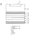
図1は、本発明の実施の形態1にかかる半導体装置10を示す図である。半導体装置10は、N型シリコン基板2を備えている。N型シリコン基板2は、一方の面にP型シリコンからなりN型シリコン基板2とPN接合を形成するアノード層1を有し、他方の面にN型シリコン層からなるカソード層3を有する。半導体装置10は、さらに、カソード層3の上に形成されチタンからなりSiTi接合を形成する第1電極膜4と、第1電極膜4の上に形成されAl−SiからなりTi−AlSi接合を形成する第2電極膜7と、第2電極膜の上に形成されNiからなりAlSi−Ni接合を形成する第3電極膜5と、第3電極膜5の上に形成されAuからなる第4電極膜6を備える。これらの電極膜により「多層電極膜」が形成されている。半導体装置10は、N型シリコン基板2の表面と裏面とにそれぞれ電極を有するダイオードである。図示しないが、アノード層1の上にさらに電極膜および保護膜が設けられていても良い。
FIG. 1 is a diagram illustrating a
図2および図3は、本発明の実施の形態1にかかる半導体装置10の作用効果を説明するための図である。図2および図3に示す矢印は、Al−Siからなる第2電極膜7とNiからなる第3電極膜5との間で互いに及ぼしあう力を模式的に図示している。実施の形態1では、Si−Ti接合(つまりカソード層3と第1電極膜4との間の接合)とNi(つまり第3電極膜5)の間にAl−Siからなる第2電極膜7を形成している。これにより、チタンシリサイドなどの反応層を形成させずに電極形成後の熱処理(例えば200度以上)を実施しても、図2および図3に示すようにSi−Tiに加わる応力を緩和でき、熱処理後もSi−Ti面剥離を抑制可能である。以上説明したように、本実施の形態によれば、アノード層1側の面に形成された構成(すなわちPN接合、電極膜、および保護膜)の機能を損なうことがなく、良好な電気特性を有するSi−Ti接合を維持しつつ、電極形成後の熱工程の際に多層電極膜に発生する応力によるSi−Ti界面剥離を抑制することができる。
2 and 3 are diagrams for explaining the function and effect of the
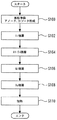
図4は、本発明の実施の形態1にかかる半導体装置10の製造方法を示すフローチャートである。先ず、N型シリコン基板2を準備し、このN型シリコン基板2にアノード層1およびカソード層3をそれぞれ形成する工程を実施する(ステップS100)。アノード層1には、他の電極膜および保護膜が設けられても良い。次に、カソード層3の上に、チタンからなる第1電極膜4を形成する工程を実施する(ステップS102)。次に、第1電極膜4の上に、Al−Siからなる第2電極膜7を形成する工程を実施する(ステップS104)。次に、第2電極膜7の上に、Niからなる第3電極膜5を形成する工程を実施する(ステップS106)。次に、第3電極膜5の上に、Auからなる第4電極膜6を形成する工程を実施する(ステップS108)。その後、多層電極形成後の熱処理(例えば200度以上)を実施する(ステップS110)。これらの工程により、図1を用いて説明した半導体装置10が得られる。
FIG. 4 is a flowchart showing a method for manufacturing the
強固なSi−Ti間の結合を得るためにチタンシリサイドなどの反応層を形成する方法があるが、その形成は700℃程度の高温プロセスが必要となる。アノード層1とアノード層1側に設けられた図示しない電極膜および保護膜とがN型シリコン基板2に形成された後でこのような高温プロセスを実施すると、それらの有すべき機能が損なわれてしまうという問題がある。そこで、本実施の形態では、そのような高温プロセスを実施しないようにしている。
There is a method of forming a reaction layer such as titanium silicide in order to obtain a strong Si-Ti bond, but the formation requires a high temperature process of about 700 ° C. When such a high-temperature process is performed after the
仮にチタンシリサイドがない状態で多層電極形成後に熱処理を実施すると、Tiからなる第1電極膜4に形成されているNiからなる第3電極膜5においてグレイン成長などによる不可逆な変化により応力が発生し、この応力が熱処理後も残存する。本実施の形態によれば、第2電極膜7が設けられているのでSi−Tiに加わる応力を緩和でき、上述したチタンシリサイドなどの反応層を形成させなくとも熱処理後におけるSi−Ti面剥離を抑制可能である。
If heat treatment is performed after forming the multilayer electrode in the absence of titanium silicide, stress is generated in the
実施の形態2.
図5は、本発明の実施の形態2にかかる半導体装置20を示す図である。半導体装置20は、第3電極膜5と第2電極膜7との間に設けられ、チタンで構成された第5電極膜9を、更に備える。これ以外の構成は実施の形態1の半導体装置10と同じである。Al−Siとはんだは合金層の形成が困難であり、はんだがAl−Siに拡散するとオーミック不良および密着強度低下による剥離が発生する。その対策として、はんだとの合金層形成膜としてNi電極膜を有しオーミック電極へのはんだ拡散防止のバリアメタル層としてTi電極膜を有する多層電極が用いられている。実施の形態1の半導体装置10に、Al−Siからなる第2電極膜7とNiからなる第3電極膜5の間に、Al−Siへのはんだ拡散防止のため、Tiからなる第5電極膜9を設けている。これにより、良好な電気特性を有するSi−Ti接合を維持しつつ、Si−Ti接合とNiの間にAl−Siを形成することができる。電極形成後の熱工程による多層電極膜から発生する応力によるSi−Ti界面剥離抑制に加え、Al−Siへのはんだ拡散を防止することによりはんだ接合性悪化を抑制できる。
FIG. 5 is a diagram showing a
図6は、本発明の実施の形態2にかかる半導体装置20の製造方法を示すフローチャートである。第3電極膜5を形成するステップS104の工程の前に、第2電極膜7の上にチタンからなる第5電極膜9を形成する工程(ステップS120)を更に備える。これ以外は図4のフローチャートに示す製造方法と同じである。
FIG. 6 is a flowchart showing a method for manufacturing the
実施の形態3.
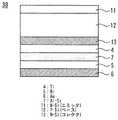
図7は、本発明の実施の形態3にかかる半導体装置30を示す図である。半導体装置30はNPNトランジスタである。半導体装置30は、一方の面にN型シリコンからなるエミッタ層11を有し他方の面にN型シリコンからなるコレクタ層13を有するP型シリコン基板12を備える。P型シリコン基板12がベース層となることで、エミッタ層11およびコレクタ層13を含むNPNトランジスタが構成される。図8は、半導体装置30の製造方法を示すフローチャートである。図4のステップS100に代えて、P型シリコン基板12の一方の面にN型シリコンからなるエミッタ層11を設け、他方の面にN型シリコンからなるコレクタ層13を設ける。これにより、実施の形態1と同様に、良好な電気特性を得つつ、P型シリコン基板12に形成された保護膜などの機能が損なわれるのを抑制し、Si−Ti面の剥離を抑制することができる。
FIG. 7 is a diagram showing a
実施の形態4.
図9は、本発明の実施の形態4にかかる半導体装置40を示す図である。半導体装置40は、半導体装置30にTiからなる第5電極膜9を追加したものである。それ以外の構成は半導体装置30と同じである。図10は、半導体装置40の製造方法を示すフローチャートである。図8のフローチャートに、実施の形態2にかかるステップS120を追加したものである。これにより、電極形成後の熱工程による多層電極膜から発生する応力によるSi−Ti界面剥離抑制に加え、Al−Siへのはんだ拡散を防止することにより、はんだ接合性悪化を抑制できる。
FIG. 9 is a diagram showing a
1 アノード層、2 N型シリコン基板、3 カソード層、4、5、6、7、9 電極膜、10、20、30、40 半導体装置、11 エミッタ層、12 P型シリコン基板、13 コレクタ層
DESCRIPTION OF
Claims (8)
前記N型シリコン層の上に、チタンからなる第1電極膜を形成することでSi−Ti接合を形成する工程と、
前記第1電極膜の上に、Al−Siからなる第2電極膜を形成する工程と、
前記第2電極膜の上に、Niからなる第3電極膜を形成する工程と、
前記第3電極膜を形成した後の前記シリコン基板を加熱する工程と、
を備え、
前記N型シリコン層と前記第1電極膜の間にチタンシリサイドが形成されていない半導体装置の製造方法。 Providing a silicon substrate having an N-type silicon layer on one side and at least one of a PN junction, an electrode film, and a protective film on the other side;
Forming a Si-Ti junction by forming a first electrode film made of titanium on the N-type silicon layer;
Forming a second electrode film made of Al-Si on the first electrode film;
Forming a third electrode film made of Ni on the second electrode film;
Heating the silicon substrate after forming the third electrode film;
With
A method of manufacturing a semiconductor device in which titanium silicide is not formed between the N-type silicon layer and the first electrode film.
チタンからなり、前記N型シリコン層の上に形成されてSi−Ti接合を形成し、前記N型シリコン層との間にチタンシリサイドを有さない第1電極膜と、
Al−Siからなり、前記第1電極膜の上に形成された第2電極膜と、
前記第2電極膜の上に形成され、Niからなる第3電極膜と、
を備える半導体装置。 A silicon substrate having an N-type silicon layer on one side and at least one of a PN junction, an electrode film, and a protective film on the other side;
A first electrode film made of titanium, formed on the N-type silicon layer to form a Si-Ti junction, and having no titanium silicide between the N-type silicon layer;
A second electrode film made of Al-Si and formed on the first electrode film;
A third electrode film formed on the second electrode film and made of Ni;
A semiconductor device comprising:
Priority Applications (4)
| Application Number | Priority Date | Filing Date | Title |
|---|---|---|---|
| JP2014081239A JP2015204301A (en) | 2014-04-10 | 2014-04-10 | Semiconductor device and method of manufacturing the same |
| US14/585,456 US9755037B2 (en) | 2014-04-10 | 2014-12-30 | Semiconductor device and method of manufacturing semiconductor device |
| DE102015202123.8A DE102015202123A1 (en) | 2014-04-10 | 2015-02-06 | Semiconductor device and method for manufacturing a semiconductor device |
| CN201510160872.9A CN104979179B (en) | 2014-04-10 | 2015-04-07 | The manufacture method of semiconductor device and semiconductor device |
Applications Claiming Priority (1)
| Application Number | Priority Date | Filing Date | Title |
|---|---|---|---|
| JP2014081239A JP2015204301A (en) | 2014-04-10 | 2014-04-10 | Semiconductor device and method of manufacturing the same |
Publications (2)
| Publication Number | Publication Date |
|---|---|
| JP2015204301A true JP2015204301A (en) | 2015-11-16 |
| JP2015204301A5 JP2015204301A5 (en) | 2016-08-04 |
Family
ID=54193404
Family Applications (1)
| Application Number | Title | Priority Date | Filing Date |
|---|---|---|---|
| JP2014081239A Pending JP2015204301A (en) | 2014-04-10 | 2014-04-10 | Semiconductor device and method of manufacturing the same |
Country Status (4)
| Country | Link |
|---|---|
| US (1) | US9755037B2 (en) |
| JP (1) | JP2015204301A (en) |
| CN (1) | CN104979179B (en) |
| DE (1) | DE102015202123A1 (en) |
Families Citing this family (2)
| Publication number | Priority date | Publication date | Assignee | Title |
|---|---|---|---|---|
| JP2017103404A (en) * | 2015-12-04 | 2017-06-08 | シャープ株式会社 | Semiconductor device and manufacturing method of the same |
| JP6494802B2 (en) * | 2016-01-19 | 2019-04-03 | 三菱電機株式会社 | Power semiconductor device and method for manufacturing power semiconductor device |
Citations (8)
| Publication number | Priority date | Publication date | Assignee | Title |
|---|---|---|---|---|
| JPS55165673A (en) * | 1979-06-12 | 1980-12-24 | Fujitsu Ltd | Semiconductor device |
| JPS6439775A (en) * | 1987-08-06 | 1989-02-10 | Fuji Electric Co Ltd | Formation of electrode film of semiconductor device |
| JPH03183126A (en) * | 1989-12-13 | 1991-08-09 | Kawasaki Steel Corp | Manufacture of semiconductor device |
| JPH0521372A (en) * | 1991-07-17 | 1993-01-29 | Nippondenso Co Ltd | Formation of electrode of semiconductor device |
| JPH0864799A (en) * | 1994-08-18 | 1996-03-08 | Toshiba Corp | Semiconductor chip, semiconductor device using it and manufacture thereof |
| JPH11274102A (en) * | 1998-03-25 | 1999-10-08 | Matsushita Electron Corp | Semiconductor device and manufacture thereof |
| JP2008004739A (en) * | 2006-06-22 | 2008-01-10 | Fuji Electric Device Technology Co Ltd | Semiconductor device |
| JP2013194291A (en) * | 2012-03-21 | 2013-09-30 | Mitsubishi Electric Corp | Semiconductor device and method for manufacturing the same |
Family Cites Families (12)
| Publication number | Priority date | Publication date | Assignee | Title |
|---|---|---|---|---|
| EP0523701B1 (en) | 1991-07-17 | 1998-01-07 | Denso Corporation | Method of forming electrodes of semiconductor device |
| DE19734434C1 (en) * | 1997-08-08 | 1998-12-10 | Siemens Ag | Semiconductor body with reverse-side metallisation e.g. for power semiconductor |
| JP3703435B2 (en) * | 2002-02-05 | 2005-10-05 | 三菱電機株式会社 | Semiconductor device |
| US8575474B2 (en) * | 2006-03-20 | 2013-11-05 | Heracus Precious Metals North America Conshohocken LLC | Solar cell contacts containing aluminum and at least one of boron, titanium, nickel, tin, silver, gallium, zinc, indium and copper |
| JP4221012B2 (en) | 2006-06-12 | 2009-02-12 | トヨタ自動車株式会社 | Semiconductor device and manufacturing method thereof |
| JP5381420B2 (en) * | 2008-07-22 | 2014-01-08 | 富士電機株式会社 | Semiconductor device |
| JP2010129585A (en) | 2008-11-25 | 2010-06-10 | Toyota Motor Corp | Method for manufacturing semiconductor device |
| DE112009004530B4 (en) * | 2009-03-23 | 2015-04-02 | Toyota Jidosha Kabushiki Kaisha | Semiconductor device |
| JP2011049393A (en) * | 2009-08-27 | 2011-03-10 | Mitsubishi Electric Corp | Semiconductor device and method of manufacturing the same |
| JP4970530B2 (en) * | 2009-12-28 | 2012-07-11 | 株式会社ノリタケカンパニーリミテド | Solar cell paste composition, method for producing the same, and solar cell |
| JP5585379B2 (en) * | 2010-10-21 | 2014-09-10 | 富士電機株式会社 | Semiconductor device manufacturing method and manufacturing apparatus thereof |
| JP5925103B2 (en) | 2012-10-15 | 2016-05-25 | 株式会社デンソーアイティーラボラトリ | Route search device, navigation device, route search method, route search program, and navigation program |
-
2014
- 2014-04-10 JP JP2014081239A patent/JP2015204301A/en active Pending
- 2014-12-30 US US14/585,456 patent/US9755037B2/en active Active
-
2015
- 2015-02-06 DE DE102015202123.8A patent/DE102015202123A1/en active Pending
- 2015-04-07 CN CN201510160872.9A patent/CN104979179B/en active Active
Patent Citations (8)
| Publication number | Priority date | Publication date | Assignee | Title |
|---|---|---|---|---|
| JPS55165673A (en) * | 1979-06-12 | 1980-12-24 | Fujitsu Ltd | Semiconductor device |
| JPS6439775A (en) * | 1987-08-06 | 1989-02-10 | Fuji Electric Co Ltd | Formation of electrode film of semiconductor device |
| JPH03183126A (en) * | 1989-12-13 | 1991-08-09 | Kawasaki Steel Corp | Manufacture of semiconductor device |
| JPH0521372A (en) * | 1991-07-17 | 1993-01-29 | Nippondenso Co Ltd | Formation of electrode of semiconductor device |
| JPH0864799A (en) * | 1994-08-18 | 1996-03-08 | Toshiba Corp | Semiconductor chip, semiconductor device using it and manufacture thereof |
| JPH11274102A (en) * | 1998-03-25 | 1999-10-08 | Matsushita Electron Corp | Semiconductor device and manufacture thereof |
| JP2008004739A (en) * | 2006-06-22 | 2008-01-10 | Fuji Electric Device Technology Co Ltd | Semiconductor device |
| JP2013194291A (en) * | 2012-03-21 | 2013-09-30 | Mitsubishi Electric Corp | Semiconductor device and method for manufacturing the same |
Also Published As
| Publication number | Publication date |
|---|---|
| DE102015202123A1 (en) | 2015-10-15 |
| CN104979179B (en) | 2018-03-16 |
| CN104979179A (en) | 2015-10-14 |
| US9755037B2 (en) | 2017-09-05 |
| US20150294871A1 (en) | 2015-10-15 |
Similar Documents
| Publication | Publication Date | Title |
|---|---|---|
| US9224645B2 (en) | Silicon carbide semiconductor device and method for manufacturing the same | |
| WO2010021136A1 (en) | Semiconductor device and semiconductor device manufacturing method | |
| WO2013125596A1 (en) | Sic semiconductor device and method for manufacturing same | |
| JPWO2017199706A1 (en) | Power semiconductor device and manufacturing method thereof | |
| JP2018133445A (en) | Semiconductor device and manufacturing method of the same | |
| WO2011099338A1 (en) | Semiconductor device and method for manufacturing semiconductor device | |
| JP2015204301A (en) | Semiconductor device and method of manufacturing the same | |
| JP6091703B2 (en) | Method for manufacturing silicon carbide semiconductor device and silicon carbide semiconductor device | |
| JPWO2015052782A1 (en) | Method for manufacturing silicon carbide semiconductor device | |
| JP2016143804A (en) | Semiconductor device | |
| JP2012248736A (en) | Semiconductor device | |
| JP2015204301A5 (en) | ||
| JP5722933B2 (en) | Laminated electrode | |
| JP2009049144A (en) | Semiconductor substrate and manufacturing method therefor | |
| JP2015165527A (en) | Semiconductor device and manufacturing method of the same | |
| JP2015056641A (en) | Semiconductor device and method of manufacturing the same | |
| JP2018056163A5 (en) | ||
| US10325776B2 (en) | Method of manufacturing semiconductor device including forming protective film within recess in substrate | |
| JP2017157776A (en) | Electrode film, semiconductor device having the same, and method of manufacturing semiconductor device | |
| JP6260711B2 (en) | Manufacturing method of semiconductor device | |
| JP2016184660A (en) | Semiconductor device and method of manufacturing the same | |
| JP2014157957A (en) | Semiconductor device | |
| JP6090474B2 (en) | Semiconductor device and manufacturing method of semiconductor device | |
| JP2015026669A (en) | Nitride semiconductor device | |
| JP2012129537A (en) | Semiconductor device |
Legal Events
| Date | Code | Title | Description |
|---|---|---|---|
| A521 | Request for written amendment filed |
Free format text: JAPANESE INTERMEDIATE CODE: A523 Effective date: 20160620 |
|
| A621 | Written request for application examination |
Free format text: JAPANESE INTERMEDIATE CODE: A621 Effective date: 20160620 |
|
| A131 | Notification of reasons for refusal |
Free format text: JAPANESE INTERMEDIATE CODE: A131 Effective date: 20170207 |
|
| A977 | Report on retrieval |
Free format text: JAPANESE INTERMEDIATE CODE: A971007 Effective date: 20170209 |
|
| A521 | Request for written amendment filed |
Free format text: JAPANESE INTERMEDIATE CODE: A523 Effective date: 20170331 |
|
| A02 | Decision of refusal |
Free format text: JAPANESE INTERMEDIATE CODE: A02 Effective date: 20170704 |