JP2012248736A - Semiconductor device - Google Patents
Semiconductor device Download PDFInfo
- Publication number
- JP2012248736A JP2012248736A JP2011120244A JP2011120244A JP2012248736A JP 2012248736 A JP2012248736 A JP 2012248736A JP 2011120244 A JP2011120244 A JP 2011120244A JP 2011120244 A JP2011120244 A JP 2011120244A JP 2012248736 A JP2012248736 A JP 2012248736A
- Authority
- JP
- Japan
- Prior art keywords
- junction
- diode
- schottky
- schottky barrier
- semiconductor device
- Prior art date
- Legal status (The legal status is an assumption and is not a legal conclusion. Google has not performed a legal analysis and makes no representation as to the accuracy of the status listed.)
- Pending
Links
- 239000004065 semiconductor Substances 0.000 title claims abstract description 116
- 230000004888 barrier function Effects 0.000 claims abstract description 70
- 239000012535 impurity Substances 0.000 claims abstract description 50
- HBMJWWWQQXIZIP-UHFFFAOYSA-N silicon carbide Chemical compound [Si+]#[C-] HBMJWWWQQXIZIP-UHFFFAOYSA-N 0.000 claims abstract description 28
- 229910010271 silicon carbide Inorganic materials 0.000 claims abstract description 27
- 229910052710 silicon Inorganic materials 0.000 claims abstract description 7
- 239000010703 silicon Substances 0.000 claims abstract description 6
- 230000015556 catabolic process Effects 0.000 claims description 19
- 230000001681 protective effect Effects 0.000 description 16
- 238000004519 manufacturing process Methods 0.000 description 14
- 238000000034 method Methods 0.000 description 13
- 239000000758 substrate Substances 0.000 description 13
- 230000008569 process Effects 0.000 description 9
- 238000011084 recovery Methods 0.000 description 6
- 229910000679 solder Inorganic materials 0.000 description 6
- 230000007423 decrease Effects 0.000 description 5
- PXHVJJICTQNCMI-UHFFFAOYSA-N nickel Substances [Ni] PXHVJJICTQNCMI-UHFFFAOYSA-N 0.000 description 5
- XUIMIQQOPSSXEZ-UHFFFAOYSA-N Silicon Chemical compound [Si] XUIMIQQOPSSXEZ-UHFFFAOYSA-N 0.000 description 4
- 230000000052 comparative effect Effects 0.000 description 4
- 238000010586 diagram Methods 0.000 description 4
- 238000005468 ion implantation Methods 0.000 description 4
- 239000002184 metal Substances 0.000 description 4
- 229910052751 metal Inorganic materials 0.000 description 4
- 229910052581 Si3N4 Inorganic materials 0.000 description 3
- BASFCYQUMIYNBI-UHFFFAOYSA-N platinum Chemical compound [Pt] BASFCYQUMIYNBI-UHFFFAOYSA-N 0.000 description 3
- HQVNEWCFYHHQES-UHFFFAOYSA-N silicon nitride Chemical compound N12[Si]34N5[Si]62N3[Si]51N64 HQVNEWCFYHHQES-UHFFFAOYSA-N 0.000 description 3
- 239000010936 titanium Substances 0.000 description 3
- 230000001133 acceleration Effects 0.000 description 2
- 230000003749 cleanliness Effects 0.000 description 2
- 238000009826 distribution Methods 0.000 description 2
- 230000005684 electric field Effects 0.000 description 2
- 230000017525 heat dissipation Effects 0.000 description 2
- 150000002500 ions Chemical class 0.000 description 2
- 230000007257 malfunction Effects 0.000 description 2
- 239000000463 material Substances 0.000 description 2
- 239000007769 metal material Substances 0.000 description 2
- 230000002093 peripheral effect Effects 0.000 description 2
- 230000006798 recombination Effects 0.000 description 2
- IJGRMHOSHXDMSA-UHFFFAOYSA-N Atomic nitrogen Chemical compound N#N IJGRMHOSHXDMSA-UHFFFAOYSA-N 0.000 description 1
- ZOKXTWBITQBERF-UHFFFAOYSA-N Molybdenum Chemical compound [Mo] ZOKXTWBITQBERF-UHFFFAOYSA-N 0.000 description 1
- RTAQQCXQSZGOHL-UHFFFAOYSA-N Titanium Chemical compound [Ti] RTAQQCXQSZGOHL-UHFFFAOYSA-N 0.000 description 1
- 230000004913 activation Effects 0.000 description 1
- 229910052782 aluminium Inorganic materials 0.000 description 1
- XAGFODPZIPBFFR-UHFFFAOYSA-N aluminium Chemical compound [Al] XAGFODPZIPBFFR-UHFFFAOYSA-N 0.000 description 1
- 238000000137 annealing Methods 0.000 description 1
- 230000015572 biosynthetic process Effects 0.000 description 1
- 238000004140 cleaning Methods 0.000 description 1
- 230000020169 heat generation Effects 0.000 description 1
- 238000010438 heat treatment Methods 0.000 description 1
- 230000004048 modification Effects 0.000 description 1
- 238000012986 modification Methods 0.000 description 1
- 229910052750 molybdenum Inorganic materials 0.000 description 1
- 239000011733 molybdenum Substances 0.000 description 1
- 229910052759 nickel Inorganic materials 0.000 description 1
- 238000005268 plasma chemical vapour deposition Methods 0.000 description 1
- 229910052697 platinum Inorganic materials 0.000 description 1
- 230000005855 radiation Effects 0.000 description 1
- 238000005215 recombination Methods 0.000 description 1
- 238000000926 separation method Methods 0.000 description 1
- 238000009751 slip forming Methods 0.000 description 1
- 229910052719 titanium Inorganic materials 0.000 description 1
Images


Classifications
-
- H—ELECTRICITY
- H01—ELECTRIC ELEMENTS
- H01L—SEMICONDUCTOR DEVICES NOT COVERED BY CLASS H10
- H01L29/00—Semiconductor devices adapted for rectifying, amplifying, oscillating or switching, or capacitors or resistors with at least one potential-jump barrier or surface barrier, e.g. PN junction depletion layer or carrier concentration layer; Details of semiconductor bodies or of electrodes thereof ; Multistep manufacturing processes therefor
- H01L29/66—Types of semiconductor device ; Multistep manufacturing processes therefor
- H01L29/86—Types of semiconductor device ; Multistep manufacturing processes therefor controllable only by variation of the electric current supplied, or only the electric potential applied, to one or more of the electrodes carrying the current to be rectified, amplified, oscillated or switched
- H01L29/861—Diodes
- H01L29/872—Schottky diodes
-
- H—ELECTRICITY
- H01—ELECTRIC ELEMENTS
- H01L—SEMICONDUCTOR DEVICES NOT COVERED BY CLASS H10
- H01L2224/00—Indexing scheme for arrangements for connecting or disconnecting semiconductor or solid-state bodies and methods related thereto as covered by H01L24/00
- H01L2224/01—Means for bonding being attached to, or being formed on, the surface to be connected, e.g. chip-to-package, die-attach, "first-level" interconnects; Manufacturing methods related thereto
- H01L2224/42—Wire connectors; Manufacturing methods related thereto
- H01L2224/47—Structure, shape, material or disposition of the wire connectors after the connecting process
- H01L2224/48—Structure, shape, material or disposition of the wire connectors after the connecting process of an individual wire connector
- H01L2224/4805—Shape
- H01L2224/4809—Loop shape
- H01L2224/48091—Arched
-
- H—ELECTRICITY
- H01—ELECTRIC ELEMENTS
- H01L—SEMICONDUCTOR DEVICES NOT COVERED BY CLASS H10
- H01L2224/00—Indexing scheme for arrangements for connecting or disconnecting semiconductor or solid-state bodies and methods related thereto as covered by H01L24/00
- H01L2224/01—Means for bonding being attached to, or being formed on, the surface to be connected, e.g. chip-to-package, die-attach, "first-level" interconnects; Manufacturing methods related thereto
- H01L2224/42—Wire connectors; Manufacturing methods related thereto
- H01L2224/47—Structure, shape, material or disposition of the wire connectors after the connecting process
- H01L2224/48—Structure, shape, material or disposition of the wire connectors after the connecting process of an individual wire connector
- H01L2224/481—Disposition
- H01L2224/48135—Connecting between different semiconductor or solid-state bodies, i.e. chip-to-chip
- H01L2224/48137—Connecting between different semiconductor or solid-state bodies, i.e. chip-to-chip the bodies being arranged next to each other, e.g. on a common substrate
-
- H—ELECTRICITY
- H01—ELECTRIC ELEMENTS
- H01L—SEMICONDUCTOR DEVICES NOT COVERED BY CLASS H10
- H01L2224/00—Indexing scheme for arrangements for connecting or disconnecting semiconductor or solid-state bodies and methods related thereto as covered by H01L24/00
- H01L2224/73—Means for bonding being of different types provided for in two or more of groups H01L2224/10, H01L2224/18, H01L2224/26, H01L2224/34, H01L2224/42, H01L2224/50, H01L2224/63, H01L2224/71
- H01L2224/732—Location after the connecting process
- H01L2224/73251—Location after the connecting process on different surfaces
- H01L2224/73265—Layer and wire connectors
Abstract
Description
本発明は、ショットキーバリアダイオードを有する半導体装置に関する。 The present invention relates to a semiconductor device having a Schottky barrier diode.
ショットキーバリアダイオード(SBD)は順方向電圧を下げやすく、スイッチング時のリカバリー電流が小さい。しかし、SBDの逆方向耐圧は低く、逆方向耐圧を高めると順方向電圧が上がるというトレードオフの特性を有する。一方、pn接合ダイオードはSBDに比べて逆方向耐圧が高いが、順方向電圧が高く、スイッチング時のリカバリー電流が大きい。 A Schottky barrier diode (SBD) is easy to lower the forward voltage and has a small recovery current during switching. However, the reverse breakdown voltage of SBD is low and has a trade-off characteristic that the forward voltage increases as the reverse breakdown voltage is increased. On the other hand, the pn junction diode has a higher reverse breakdown voltage than the SBD, but has a high forward voltage and a large recovery current during switching.
これらの問題を改善するダイオードとして、ファーストリカバリーダイオード(FRD)がある。FRDでは、pn接合部分にバイポーラ電流の再結合中心が形成され、スイッチング時のリカバリー電流が抑制される。再結合中心を多く注入するとリカバリー電流は抑制されるが、逆方向電圧印加時のリーク電流が増加し、順方向電圧が上昇する。 As a diode for improving these problems, there is a fast recovery diode (FRD). In FRD, a recombination center of bipolar current is formed at a pn junction, and a recovery current at the time of switching is suppressed. When a large number of recombination centers are injected, the recovery current is suppressed, but the leakage current increases when the reverse voltage is applied, and the forward voltage increases.
また、SBDにpn接合領域を付加し、ショットキー接合とpn接合を併設したMPS(Merged PiN Schottoky)構造のダイオードは、SBDにおいて順方向特性を改善した素子である。SBDはモノポーラ伝導素子であるため、順方向特性は線形であり、順方向サージ電流に対する破壊耐量(順方向サージ耐量)が小さい。一方、pn接合領域に形成されるpn接合ダイオードはバイポーラ伝導素子であり、電圧上昇に伴って順方向電流が非線形で急激に増大するため、SBDに比べて順方向サージ耐量が高い。つまり、MPS構造のダイオードでは、ショットキー接合とpn接合を併設することにより、順方向サージ耐量が改善される(例えば、特許文献1参照。)。 In addition, a diode having an MPS (Merged PiN Schottoky) structure in which a pn junction region is added to the SBD and a Schottky junction and a pn junction are provided is an element having improved forward characteristics in the SBD. Since the SBD is a monopolar conductive element, the forward characteristics are linear, and the breakdown resistance against the forward surge current (forward surge resistance) is small. On the other hand, the pn junction diode formed in the pn junction region is a bipolar conduction element, and since the forward current increases nonlinearly and rapidly with increasing voltage, the forward surge resistance is higher than that of SBD. That is, in a diode having an MPS structure, the forward surge resistance is improved by providing a Schottky junction and a pn junction (see, for example, Patent Document 1).
シリコン(Si)からなる半導体装置についてのみでなく、シリコンカーバイト(SiC)からなる半導体装置についても、上記と同様の特徴がある。SiCはSiに比べてバンドギャップが3倍程度大きく、絶縁破壊強度が10倍程度大きい。このため、Siからなる半導体装置に比べて、SiCからなる半導体装置では耐圧用の層の膜厚を大幅に薄く、高不純物濃度にすることができる。その結果、高耐圧、低抵抗の素子を形成可能である。 Not only the semiconductor device made of silicon (Si) but also the semiconductor device made of silicon carbide (SiC) has the same characteristics as described above. SiC has a band gap of about 3 times larger than Si and a dielectric breakdown strength of about 10 times larger. For this reason, compared with a semiconductor device made of Si, in a semiconductor device made of SiC, the thickness of the withstand voltage layer can be significantly reduced, and a high impurity concentration can be achieved. As a result, a high breakdown voltage, low resistance element can be formed.
SiC半導体のSBDでは、Si半導体のFRDと同等以上の順方向電圧及び逆方向耐圧を得られ、リカバリー電流を大幅に低減できる。しかし、SiC半導体のSBDは、Si半導体のFRDに比べて、順方向電流が同一の場合の素子面積は1/10程度である。このため、SiC半導体のSBDの定格電流密度はSi半導体のFRDの10倍程度であり、更に大きな電流駆動が要求される順方向サージ耐量が定格電流の10倍程度と低い。 In the SBD of the SiC semiconductor, the forward voltage and the reverse breakdown voltage equal to or higher than those of the Si semiconductor FRD can be obtained, and the recovery current can be greatly reduced. However, the SBD of the SiC semiconductor has an element area of about 1/10 when the forward current is the same as that of the FR of the Si semiconductor. For this reason, the rated current density of the SBD of the SiC semiconductor is about 10 times that of the FR of the Si semiconductor, and the forward surge resistance that requires a larger current drive is as low as about 10 times the rated current.
SiC半導体のSBDについて順方向サージ耐量を高める方法として、MPS構造を採用することが有効である。ただし、MPS構造では、pn接合を構成する高濃度不純物領域と金属電極とのコンタクト抵抗を低減する必要がある。コンタクト抵抗が十分に小さくない場合、pn接合に加わる電圧が低下して、pn接合ダイオードがバイポーラ動作した際に大きなバイポーラ電流が流れにくいためである。このため、高濃度不純物領域と金属電極との間にコンタクト電極が形成される。 It is effective to adopt the MPS structure as a method for increasing the forward surge withstand capability for the SBD of the SiC semiconductor. However, in the MPS structure, it is necessary to reduce the contact resistance between the high concentration impurity region forming the pn junction and the metal electrode. This is because when the contact resistance is not sufficiently small, the voltage applied to the pn junction decreases, and a large bipolar current hardly flows when the pn junction diode performs a bipolar operation. Therefore, a contact electrode is formed between the high concentration impurity region and the metal electrode.
しかし、ショットキー接合を形成する領域上にコンタクト電極を形成し、更にこのコンタクト電極を除去する工程により、ショットキー接合面の清浄度が低下する。その結果、SiC半導体のSBDを有する半導体装置の歩留まりが低下するという問題があった。 However, the cleanliness of the Schottky junction surface is reduced by forming the contact electrode on the region where the Schottky junction is to be formed and further removing the contact electrode. As a result, there is a problem that the yield of the semiconductor device having the SBD of SiC semiconductor is lowered.
上記問題点に鑑み、本発明は、SiC半導体からなるSBDを有し、歩留まりの高い半導体装置を提供することを目的とする。 In view of the above problems, an object of the present invention is to provide a semiconductor device having an SBD made of a SiC semiconductor and having a high yield.
本発明の一態様によれば、(イ)第1のダイパットと第2のダイパットが互いに離間して配置されたパッケージと、(ロ)第1のダイパット上に搭載された、シリコンカーバイトからなる半導体層を有し、ショットキー接合とpn接合が併設されたショットキーバリアダイオードと、(ハ)ショットキーバリアダイオードと並列接続されて第2のダイパット上に搭載された、シリコンからなる半導体層を有するpn接合ダイオードとを備え、ショットキーバリアダイオードにおいてpn接合を構成する高濃度不純物領域とショットキー接合を構成するショットキー電極とが直接に接している半導体装置が提供される。 According to one aspect of the present invention, it comprises (a) a package in which a first die pad and a second die pad are spaced apart from each other, and (b) a silicon carbide mounted on the first die pad. A Schottky barrier diode having a semiconductor layer and provided with a Schottky junction and a pn junction; and (c) a semiconductor layer made of silicon mounted in parallel with the Schottky barrier diode and mounted on the second die pad. There is provided a semiconductor device including a pn junction diode having a high concentration impurity region forming a pn junction and a Schottky electrode forming a Schottky junction in the Schottky barrier diode.
本発明によれば、SiC半導体からなるSBDを有し、歩留まりの高い半導体装置を提供できる。 According to the present invention, a semiconductor device having an SBD made of a SiC semiconductor and having a high yield can be provided.
次に、図面を参照して、本発明の実施形態を説明する。以下の図面の記載において、同一又は類似の部分には同一又は類似の符号を付している。ただし、図面は模式的なものであり、各層の厚みの比率等は現実のものとは異なることに留意すべきである。したがって、具体的な厚みや寸法は以下の説明を参酌して判断すべきものである。又、図面相互間においても互いの寸法の関係や比率が異なる部分が含まれていることはもちろんである。 Next, an embodiment of the present invention will be described with reference to the drawings. In the following description of the drawings, the same or similar parts are denoted by the same or similar reference numerals. However, it should be noted that the drawings are schematic, and the ratio of the thickness of each layer is different from the actual one. Therefore, specific thicknesses and dimensions should be determined in consideration of the following description. Moreover, it is a matter of course that portions having different dimensional relationships and ratios are included between the drawings.
又、以下に示す実施形態は、この発明の技術的思想を具体化するための装置や方法を例示するものであって、この発明の実施形態は、構成部品の材質、形状、構造、配置等を下記のものに特定するものでない。この発明の実施形態は、特許請求の範囲において、種々の変更を加えることができる。 Further, the embodiments described below exemplify apparatuses and methods for embodying the technical idea of the present invention, and the embodiments of the present invention include the material, shape, structure, arrangement, etc. of the component parts. Is not specified as follows. The embodiment of the present invention can be variously modified within the scope of the claims.
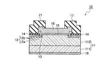
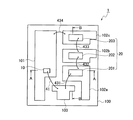
本発明の実施形態に係る半導体装置1は、図1に示すように、第1のダイパット101と第2のダイパット102が互いに離間して配置されたパッケージ100と、第1のダイパット101上に搭載された、シリコンカーバイトからなる半導体層を有するショットキーバリアダイオード10と、ショットキーバリアダイオード10と並列接続されて第2のダイパット102上に搭載された、シリコンからなる半導体層を有するpn接合ダイオード20とを備える。後述するように、ショットキーバリアダイオード10においてpn接合を構成する高濃度不純物領域とショットキー接合を構成するショットキー電極とは、直接に接している。
As shown in FIG. 1, the
まず、ショットキーバリアダイオード10について説明する。図2に示すように、SiCからなる第1導電型の高濃度不純物基板111上にSiCからなる第1導電型の半導体層112が積層されて、第1導電型の半導体積層体11が形成されている。半導体層112の周辺領域の上面の一部に、複数の第2導電型の不純物領域12が互いに離間して埋め込まれている。不純物領域12のうち、半導体層112の中央部に近い領域に形成された不純物領域12aの上面の一部に、第2導電型の高濃度不純物領域13が埋め込まれている。
First, the
更に、半導体層112の上面の外縁部に表面保護膜14が配置され、表面保護膜14の開口部で半導体層112に接してショットキー電極15が表面保護膜14上に配置されている。表面保護膜14の開口部の周辺部において、高濃度不純物領域13とショットキー電極15とが接している。ショットキー電極15上に、表面電極16が配置されている。表面電極16の中央領域が露出するように、表面電極16の上面の周辺、及びショットキー電極15と表面電極16の側面を覆って素子保護膜17が配置されている。また、高濃度不純物基板111の半導体層112が形成された面と対向する面に、裏面電極18が形成されている。
Further, the surface
第1導電型と第2導電型とは互いに反対導電型である。すなわち、第1導電型がn型であれば、第2導電型はp型であり、第1導電型がp型であれば、第2導電型はn型である。ここでは、第1導電型がn型、第2導電型がp型であるとする。したがって、ショットキーバリアダイオード10において、表面電極16がアノード端子、裏面電極18がカソード端子である。
The first conductivity type and the second conductivity type are opposite to each other. That is, if the first conductivity type is n-type, the second conductivity type is p-type, and if the first conductivity type is p-type, the second conductivity type is n-type. Here, it is assumed that the first conductivity type is n-type and the second conductivity type is p-type. Therefore, in the
ショットキーバリアダイオード10では、不純物領域12の形成された領域の残余の領域において半導体層112とショットキー電極15とが接触する領域にショットキーバリアダイオードが形成されている。ショットキーバリアダイオードが形成される領域を、「ショットキー接合部分」という。また、高濃度不純物領域13が埋め込まれた不純物領域12aと半導体層112とが接触する領域に、pn接合ダイオードが形成されている。pn接合ダイオードが形成される領域を、「pn接合部分」という。なお、不純物領域12のうち、半導体層112の上面の周辺で表面保護膜14と接する不純物領域12bは、ガードリングとして機能する。
In the
一般的に、MPS構造を有する半導体装置では、pn接合ダイオードがバイポーラ動作することによって、SBD単体に比べて順方向サージ耐量が改善される。即ち、n型半導体層にp型半導体層から正孔が注入されることにより、n型半導体層中の電子が本来の不純物濃度以上の高濃度になる。これにより半導体装置に大電流が流れて、順方向サージ耐量が改善される。 In general, in a semiconductor device having an MPS structure, the forward surge withstand capability is improved as compared with a single SBD because the pn junction diode performs a bipolar operation. That is, by injecting holes from the p-type semiconductor layer into the n-type semiconductor layer, electrons in the n-type semiconductor layer have a higher concentration than the original impurity concentration. As a result, a large current flows through the semiconductor device, and the forward surge resistance is improved.
ショットキーバリアダイオード10においては、pn接合部分の半導体積層体11の上面にショットキー電極15が直接に配置されている。即ち、pn接合部分とショットキー接合部分に渡って、半導体積層体11の上面にショットキー電極15が連続的に形成されている。したがって、pn接合部分を形成する高濃度不純物領域13とショットキー接合部分を形成するショットキー電極15とは直接に接しており、高濃度不純物領域13とショットキー電極15との間にコンタクト電極は形成されていない。
In the
図2に示したショットキーバリアダイオード10の製造方法の例を、図3から図9を参照して説明する。
An example of a method for manufacturing the
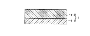
図3に示すように、SiCからなるn型の高濃度不純物基板111上に、所望の耐圧に適した濃度のn型の半導体層112を形成して、半導体積層体11を構成する。例えば、高濃度不純物基板111は不純物濃度が5×10¹⁷〜5×1018cm-3程度のSiC基板であり、半導体層112はSiC基板上にエピタキシャル成長された膜厚4μm〜50μm、不純物濃度1×10¹⁵〜5×1016cm-3程度のSiC半導体層である。
As shown in FIG. 3, an n-
図4に示すように、例えばアルミニウム(Al)などのp型の不純物をイオン注入して、p型の不純物領域12を半導体層112に形成する。不純物領域12を形成するイオン注入条件は、例えば加速エネルギー500keV、ドーズ量2×1013cm-2でAlイオンを注入する。
As shown in FIG. 4, for example, a p-
次いで、図5に示すように、pn接合部分の不純物領域12aの表面にイオン注入などによって高濃度不純物領域13を形成する。高濃度不純物領域13を形成するためのAlイオンのイオン注入条件は、例えば加速エネルギー50keV、100keV、150keVで各ドーズ量5×1014cm-2、1×1015cm-2、1×1015cm-2である。イオン注入された層の活性化のために、1800℃、10分間程度の熱処理を行う。
Next, as shown in FIG. 5, a high
活性化後の表面ダメージと以降の工程での表面保護を目的として、図6に示すように、半導体積層体11の表面に表面保護膜14を形成し、高濃度不純物基板111の裏面に裏面保護膜141を形成する。表面保護膜14及び裏面保護膜141は、例えば膜厚50nmの熱酸化膜である。そして、図7に示すように、裏面保護膜141を除去した後、高濃度不純物基板111の裏面に裏面電極18を形成する。裏面電極18には、高濃度不純物基板111とオーミック接合を形成する金属材料などを採用可能である。例えば膜厚100nmのNi膜を形成し、窒素(N2)雰囲気中で1000℃、5分間のアニールを行って、裏面電極18を形成する。
For the purpose of surface damage after activation and surface protection in the subsequent steps, as shown in FIG. 6, a surface
その後、図8に示すようにショットキー接合部分及びpn接合部分の表面保護膜14を除去して開口部140を形成する。そして、図9に示すように、開口部140で半導体積層体11と接するように、ショットキー電極15を形成する。ショットキー電極15には、半導体層112との界面にショットキーバリア接合を形成する金属材料などを採用可能である。例えば、チタン(Ti)膜、ニッケル(Ni)膜、モリブデン(Mo)膜、白金(Pt)膜などをショットキー電極15に採用可能である。ショットキー電極15の膜厚は、100nm程度である。
Thereafter, as shown in FIG. 8, the surface
更に、ショットキー電極15上に表面電極16を形成する。表面電極16には、例えば膜厚5μm程度のAl膜などを採用可能である。
Further, the
次いで、窒化シリコン(SiN)膜などを素子保護膜17として形成する。例えば、SiH4とNH3を用いたプラズマCVD法により、膜厚500nm程度のSiN膜を形成する。そして、表面電極16上の素子保護膜17を除去して表面電極16の上面を露出させて、図2に示したショットキーバリアダイオード10が完成する。
Next, a silicon nitride (SiN) film or the like is formed as the element
上記に説明したショットキーバリアダイオード10の製造方法とは異なり、一般的には、MPS構造の半導体装置では、pn接合部分の高濃度不純物領域13とショットキー電極15とのコンタクト抵抗を低減するために、高濃度不純物領域13とショットキー電極15との間にコンタクト電極が形成される。
Unlike the manufacturing method of the
具体的には、図6に示したように高濃度不純物領域13が形成された半導体積層体11の上面全体に表面保護膜14を形成した後、図10に示すように、高濃度不純物領域13上で表面保護膜14に開口部を形成し、この開口部を埋め込むようにして高濃度不純物領域13上にコンタクト電極150を形成する。例えば、Ti膜、Al膜、Ni膜などの金属膜を形成した後、この金属膜をシリサイド化してコンタクト電極150を形成する。
Specifically, after the surface
コンタクト電極150の抵抗値を低減するために例えば1000℃程度でのアニールを行った後、図11に示すように、ショットキー接合部分上の表面保護膜14を除去して開口部140を形成する。その後、図9と同様にショットキー電極15と表面電極16を形成する。その結果、高濃度不純物領域13とショットキー電極15との間にコンタクト電極150が配置される。
In order to reduce the resistance value of the
これに対して、図2に示したショットキーバリアダイオード10では、高濃度不純物領域13とショットキー電極15との間にコンタクト電極は配置されない。つまり、ショットキー接合部分にコンタクト電極を形成し、更に除去する工程がないため、例えばコンタクト電極用の材料がショットキー接合部分に残ることなどによって、ショットキー障壁が低くなるなどの問題が生じない。このため、ショットキー電極15形成前の無機洗浄などにより、ショットキー接合部分の清浄度を十分に高くすることができる。その結果、ショットキーバリアダイオード10の製造歩留まりが向上する。
On the other hand, in the
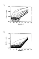
図12(a)に、SiCからなり、コンタクト電極150を有するMPS構造の半導体装置(以下において、「MPS素子」という。)の逆方向リーク電流の例を示す。図12(b)に、ショットキーバリアダイオード10の逆方向リーク電流の例を示す。図12(a)と図12(b)とを比較して明らかなように、ショットキーバリアダイオード10によれば、逆方向リーク電流のバラツキが小さく抑えられている。
FIG. 12A shows an example of reverse leakage current of an MPS structure semiconductor device (hereinafter referred to as “MPS element”) made of SiC and having a
図13に、逆方向電圧が600Vでの逆方向リーク電流分布の例を示す。図13において、黒丸がショットキーバリアダイオード10の特性A、白丸がMPS素子の特性Bである。例えば1×10⁻⁶Aを逆方向リーク電流の上限とした場合、MPS素子の歩留まりが25%程度であるのに対し、図2に示したショットキーバリアダイオード10の歩留まりは80%程度であり、3倍以上である。
FIG. 13 shows an example of the reverse leakage current distribution when the reverse voltage is 600V. In FIG. 13, the black circle is the characteristic A of the
更に、ショットキーバリアダイオード10では、pn接合部分はショットキー接合部分の周囲にのみ形成され、更に、コンタクト電極150は形成されない。これに対し、一般的なMPS構造では、pn接合部分とショットキー接合部分が混在し、pn接合部分にコンタクト電極150を形成する。このため、ショットキーバリアダイオード10では、一般的なMPS構造の半導体装置と比較してラフな加工精度での加工が可能であり、製造工程を簡略化することもできる。
Further, in the
図14に、ショットキーバリアダイオード、pn接合ダイオード、MPS素子、及び図1に示した半導体装置1の、順方向特性の例を示す。図14において、特性Aがショットキーバリアダイオード、特性BがMPS素子、特性Cがpn接合ダイオード、特性Dが半導体装置1の順方向特性である。
FIG. 14 shows examples of forward characteristics of the Schottky barrier diode, the pn junction diode, the MPS element, and the
MPS素子は、低電圧ではショットキー接合部分を流れる電流(以下において、「SBD電流」という。)が支配的で、高電圧ではpn接合部分を流れる電流(以下において、「pn接合電流」という。)が支配的である。これは、n型基板及びn型半導体層を共通カソードとして使用しているためである。低電圧ではショットキー接合がオンし、SBD電流が流れて基板抵抗による電圧降下が起こる。この電圧降下により、pn接合に印加される電圧が、pn接合ダイオードが単独で動作する場合と比べて低下する。その結果、pn接合電流が流れにくく、SBD電流が支配的となる。pn接合に加わる電圧が上昇してpn接合部分に電流が流れ始めると、n型の半導体層112にp型の高濃度不純物領域13からホール(正孔)注入が起こり、半導体層112の抵抗が減少する。これにより、高電圧では、pn接合電流が支配的になる。
The MPS element has a dominant current (hereinafter referred to as “SBD current”) flowing through the Schottky junction portion at a low voltage, and is referred to as “pn junction current” below at a high voltage. ) Is dominant. This is because the n-type substrate and the n-type semiconductor layer are used as a common cathode. At a low voltage, the Schottky junction is turned on, an SBD current flows, and a voltage drop due to the substrate resistance occurs. Due to this voltage drop, the voltage applied to the pn junction decreases as compared to the case where the pn junction diode operates alone. As a result, the pn junction current hardly flows and the SBD current becomes dominant. When the voltage applied to the pn junction rises and current starts to flow in the pn junction, holes are injected into the n-
一方、ショットキーバリアダイオード10においては、ショットキー電極15と高濃度不純物領域13とのコンタクト抵抗が高い。このため、pn接合に加わる電圧が低下し、pn接合ダイオードがバイポーラ動作した後に流れるバイポーラ電流が流れにくい。その結果、ショットキーバリアダイオード10単体では順方向サージ耐量が低下する。
On the other hand, in the
しかし、半導体装置1は、pn接合部分にコンタクト電極を形成しないショットキーバリアダイオード10と、順方向サージ耐量が十分に大きなシリコン基板のpn接合ダイオード20とが、並列接続された構造を有する。したがって、半導体装置1では、並列接続されたショットキーバリアダイオード10とpn接合ダイオード20にそれぞれの面積に応じた順方向電流が流れ、その和が半導体装置1に流れる総電流である。このため、半導体装置1では、MPS素子よりも順方向サージ耐量が向上する。
However, the
なお、ショットキーバリアダイオード10においては、pn接合部分が形成されることによって逆方向耐圧が向上する。特に、電界が集中するショットキー接合部分の周囲に、pn接合部分が形成されている。このとき、pn接合部分の不純物領域12aの電位がフローティングであると外周部での電界集中を緩和しづらいため、高濃度不純物領域13はショットキー電極15と電気的に接続されている。
In the
半導体装置1のpn接合ダイオード20には、順方向サージ耐量が十分に大きなpn接合ダイオードが使用される。更に、ショットキーバリアダイオード10の特性に合わせて、最適な特性のpn接合ダイオード20が選択される。例えば、MPS素子と同等の順・逆方向特性やスイッチング特性を有するpn接合ダイオード20が使用される。
As the
図15に、図14に示した特性Dを有する半導体装置1の等価回路図を示す。図15に示したpn接合ダイオード20は、ショットキーバリアダイオード10と並列に、複数のpn接合ダイオード素子を直列接続した構成である。具体的には、pn接合ダイオード素子201〜203が直列接続されて、pn接合ダイオード20が構成されている。3つのpn接合ダイオード素子を用いてpn接合ダイオード20を構成したのは、例えば600V以上の逆方向耐圧を有するショットキーバリアダイオード10の順方向電圧が約1.5V以上であるのに対し、pn接合ダイオード素子201〜203それぞれの順方向電圧が0.7V程度であるためである。pn接合ダイオード20はサージ電流が流れる場合にのみ導通状態になればよいため、pn接合ダイオード20の順方向電圧をショットキーバリアダイオード10の順方向電圧よりも大きくすることが好ましい。このため、pn接合ダイオード20においては2V以上で順方向電流が流れるように、pn接合ダイオード素子を3個直列に接続する必要がある。
FIG. 15 shows an equivalent circuit diagram of the
したがって、ショットキーバリアダイオード10の特性に応じてpn接合ダイオード20を構成するpn接合ダイオード素子の数は選択され、その数が3個に限られないことはもちろんである。なお、各pn接合ダイオード素子の逆方向耐圧は200V以上とする。これにより、pn接合ダイオード20の逆方向耐圧をショットキーバリアダイオード10の逆方向耐圧と同等にできる。
Therefore, the number of pn junction diode elements constituting the
更に、半導体装置1の逆方向サージ耐量も向上させるためには、ショットキーバリアダイオード10よりも低い電圧でpn接合ダイオード20がアバランシェ降伏する必要がある。例えば、ショットキーバリアダイオード10のアバランシェ耐圧が800Vである場合、pn接合ダイオード20が700V程度でアバランシェ降伏するように耐圧設計を行う。
Furthermore, in order to improve the reverse surge withstand capability of the
なお、Si半導体を用いてpn接合ダイオード20を形成した場合、チップ面積を大きくすることにより、SiC半導体を用いたSBDと比較して順方向サージ電流の電流密度を一桁程度低減することができる。また、pn接合ダイオード20を複数のpn接合ダイオード素子を直列接続した構成にすることにより、順方向サージ電流が流れた場合の放熱面積を大きくすることができる。このため、順方向サージ耐量を大幅に向上することができる。
When the
図16(a)に、図1のA−A方向に沿った断面図を示す。また、図16(b)に、図1のB−B方向に沿った断面図を示す。ショットキーバリアダイオード10のカソード端子10kである裏面電極18が、半田31を介して第1のダイパット101に電気的に接続されている。また、ショットキーバリアダイオード10のアノード端子10aである表面電極16と半導体装置1のアノード端子103とが、ワイヤ41により電気的に接続されている。第1のダイパット101は、半導体装置1のカソード端子を兼ねている。
FIG. 16A shows a cross-sectional view along the direction AA in FIG. Further, FIG. 16B shows a cross-sectional view along the BB direction of FIG. The
また、図16(a)及び図16(b)に示すように、pn接合ダイオード素子201、202が絶縁シート50を介して第2のダイパット102に搭載されている。pn接合ダイオード素子201のカソード端子201kとpn接合ダイオード素子202のアノード端子202aとは、絶縁シート50上の半田321によって電気的に接続されている。pn接合ダイオード素子201のアノード端子201aは、ワイヤ421によって半導体装置1のアノード端子103に接続されている。また、pn接合ダイオード素子202のカソード端子202kは、ワイヤ422によってpn接合ダイオード素子203のアノード端子203aに接続されている。pn接合ダイオード素子203のカソード端子203kは、半田322を介して第2のダイパット102と電気的に接続されている。第2のダイパット102は、ワイヤ423によって第1のダイパット101と電気的に接続されている。
In addition, as shown in FIGS. 16A and 16B, pn
上記のように、半導体装置1では、第2のダイパット102上で直列接続されたpn接合ダイオード素子201〜203と、ショットキーバリアダイオード10とが、並列接続されている。
As described above, in the
ショットキーバリアダイオード10が搭載される第1のダイパット101と、pn接合ダイオード20が搭載される第2のダイパット102とは、物理的に分離されている。これにより、ショットキーバリアダイオード10から発生する熱がpn接合ダイオード20に伝導するのが抑制され、pn接合ダイオード20の動作が安定する。
The
例えば、定常動作中にデューティ50%の100Aのパルス電流が半導体装置1に流れた場合、順方向電圧が1.5Vのショットキーバリアダイオード10では平均75W程度の電力消費がある。パッケージ100の放熱が2℃/Wであると、室温25℃でのショットキーバリアダイオード10のチップ温度は175℃である。第1のダイパット101と第2のダイパット102とが接触した状態では、第1のダイパット101と第2のダイパット102とはほぼ同温である。このため、pn接合ダイオード20のチップ温度が175℃近くまで上昇する。Si半導体素子の場合、150℃以上の高温では半導体特性が失われ、動作不良を起こす。したがって、第1のダイパット101と第2のダイパット102とが分離されていることは、半導体装置1を正常動作させる上で有効である。
For example, when a pulse current of 100 A with a duty of 50% flows through the
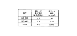
図17に、逆方向耐圧が600V、順方向定格電流が10Aである半導体装置の順方向サージ電流及び逆方向サージ耐量の比較を示す。図17で、素子「SiC−SBD」はSiC半導体からなるSBDであり、ショットキーバリアダイオード10に相当する。素子「SiC−MPS」はSiC半導体からなるMPS素子である。素子「Si−PN」はSi半導体からなるpn接合ダイオードであり、pn接合ダイオード20に相当する。
FIG. 17 shows a comparison between the forward surge current and the reverse surge withstand capability of a semiconductor device having a reverse breakdown voltage of 600 V and a forward rated current of 10 A. In FIG. 17, the element “SiC-SBD” is an SBD made of a SiC semiconductor and corresponds to the
図17においては、順方向の最大サージ電流を、順方向定格電流に対する倍数で示している。SiC−SBDの逆方向サージ耐量が100mJ/cm2であるのに対し、SiC−MPSの逆方向サージ耐量は2J/cm2であり、SiC−SBDの20倍程度である。更に、Si−PNの逆方向サージ耐量は20J/cm2であり、SiC−MPSの10倍である。同一電流ではSi半導体素子の素子面積がSiC半導体素子よりも約10倍大きいため、電流密度が1/10以下になり、サージ耐量が向上する。 In FIG. 17, the maximum forward surge current is shown as a multiple of the forward rated current. The reverse surge resistance of SiC-SBD is 100 mJ / cm 2 , whereas the reverse surge resistance of SiC-MPS is 2 J / cm 2, which is about 20 times that of SiC-SBD. Furthermore, the reverse surge resistance of Si-PN is 20 J / cm 2, which is 10 times that of SiC-MPS. Since the element area of the Si semiconductor element is about 10 times larger than that of the SiC semiconductor element at the same current, the current density becomes 1/10 or less and the surge resistance is improved.
図18に、本発明の実施形態の変形例に係る半導体装置1を示す。図18に示した例では、pn接合ダイオード20を構成するpn接合ダイオード素子201〜203が、第2のダイパット102を分割したダイパット102a〜102cにそれぞれ搭載されている。図19(a)に図18のA−A方向に沿った断面図を示し、図19(b)に図18のB−B方向に沿った断面図を示す。
FIG. 18 shows a
図19(a)及び図19(b)に示すように、pn接合ダイオード素子201のカソード端子201kが半田331を介してダイパット102aに接続され、pn接合ダイオード素子202のカソード端子202kが半田332を介してダイパット102bに接続され、pn接合ダイオード素子203のカソード端子203kが半田333を介してダイパット102cに接続されている。pn接合ダイオード素子201のアノード端子201aはワイヤ431によってアノード端子103に接続され、pn接合ダイオード素子202のアノード端子202aはワイヤ432によってダイパット102aに接続され、pn接合ダイオード素子203のアノード端子203aはワイヤ433によってダイパット102bに接続されている。更に、ワイヤ434によってダイパット102cと第1のダイパット101が接続されている。これにより、直列接続されたpn接合ダイオード素子201〜203と、ショットキーバリアダイオード10とが、並列接続される。
As shown in FIGS. 19A and 19B, the
図18に示した半導体装置1では、pn接合ダイオード素子201〜203は絶縁シートを介さずにダイパット102a〜102cにそれぞれ搭載されている。このため、放熱効率が高い。したがって、図18に示した半導体装置1は高温時の安定性が高い。
In the
以上に説明したように、本発明の実施形態に係る半導体装置1では、SiCからなる半導体層を有するショットキーバリアダイオード10と、Siからなる半導体層を有するpn接合ダイオード20とが並列接続されて、整流機能を実現している。半導体装置1にサージ電流が流れた場合のバイポーラ動作は、pn接合ダイオード20で行われる。このため、ショットキーバリアダイオード10におけるコンタクト電極は不要である。したがって、ショットキーバリアダイオード10の製造において、高濃度不純物領域13とショットキー電極15との間にコンタクト電極を形成する工程及びこのコンタクト電極を削除する工程は行われない。その結果、ショットキーバリアダイオード10の歩留まりを向上させることができる。
As described above, in the
したがって、半導体装置1によれば、SiC半導体からなるショットキーバリアダイオード10を有し、且つ歩留まりの高い半導体装置を提供することができる。
Therefore, according to the
また、ショットキーバリアダイオード10を第1のダイパット101に搭載し、pn接合ダイオード20を第2のダイパット102に搭載することにより、ショットキーバリアダイオード10の発熱によってpn接合ダイオード20が動作不良を起こすことを防止できる。つまり、第1のダイパット101と第2のダイパット102とを分離することにより、半導体装置1の動作をより安定させることができる。
Further, by mounting the
上記のように本発明は実施形態によって記載したが、この開示の一部をなす論述及び図面はこの発明を限定するものであると理解すべきではない。この開示から当業者には様々な代替実施形態、実施例及び運用技術が明らかとなろう。即ち、本発明はここでは記載していない様々な実施形態等を含むことは勿論である。したがって、本発明の技術的範囲は上記の説明から妥当な特許請求の範囲に係る発明特定事項によってのみ定められるものである。 As described above, the present invention has been described according to the embodiments. However, it should not be understood that the descriptions and drawings constituting a part of this disclosure limit the present invention. From this disclosure, various alternative embodiments, examples and operational techniques will be apparent to those skilled in the art. That is, it goes without saying that the present invention includes various embodiments not described herein. Therefore, the technical scope of the present invention is defined only by the invention specifying matters according to the scope of claims reasonable from the above description.
1…半導体装置
10…ショットキーバリアダイオード
11…半導体積層体
12…不純物領域
13…高濃度不純物領域
14…表面保護膜
15…ショットキー電極
16…表面電極
17…素子保護膜
18…裏面電極
20…pn接合ダイオード
50…絶縁シート
100…パッケージ
101…第1のダイパット
102…第2のダイパット
102a〜102c…ダイパット
111…高濃度不純物基板
112…半導体層
141…裏面保護膜
150…コンタクト電極
201〜203…pn接合ダイオード素子
DESCRIPTION OF
Claims (7)
前記第1のダイパット上に搭載された、シリコンカーバイトからなる半導体層を有し、ショットキー接合とpn接合が併設されたショットキーバリアダイオードと、
前記ショットキーバリアダイオードと並列接続されて前記第2のダイパット上に搭載された、シリコンからなる半導体層を有するpn接合ダイオードと
を備え、前記ショットキーバリアダイオードにおいて前記pn接合を構成する高濃度不純物領域と前記ショットキー接合を構成するショットキー電極とが直接に接していることを特徴とする半導体装置。 A package in which the first die pad and the second die pad are spaced apart from each other;
A Schottky barrier diode mounted on the first die pad and having a semiconductor layer made of silicon carbide and provided with a Schottky junction and a pn junction;
A pn junction diode having a semiconductor layer made of silicon and mounted in parallel with the Schottky barrier diode and mounted on the second die pad, and a high-concentration impurity constituting the pn junction in the Schottky barrier diode A semiconductor device, wherein a region and a Schottky electrode constituting the Schottky junction are in direct contact with each other.
Priority Applications (1)
| Application Number | Priority Date | Filing Date | Title |
|---|---|---|---|
| JP2011120244A JP2012248736A (en) | 2011-05-30 | 2011-05-30 | Semiconductor device |
Applications Claiming Priority (1)
| Application Number | Priority Date | Filing Date | Title |
|---|---|---|---|
| JP2011120244A JP2012248736A (en) | 2011-05-30 | 2011-05-30 | Semiconductor device |
Publications (1)
| Publication Number | Publication Date |
|---|---|
| JP2012248736A true JP2012248736A (en) | 2012-12-13 |
Family
ID=47468911
Family Applications (1)
| Application Number | Title | Priority Date | Filing Date |
|---|---|---|---|
| JP2011120244A Pending JP2012248736A (en) | 2011-05-30 | 2011-05-30 | Semiconductor device |
Country Status (1)
| Country | Link |
|---|---|
| JP (1) | JP2012248736A (en) |
Cited By (5)
| Publication number | Priority date | Publication date | Assignee | Title |
|---|---|---|---|---|
| KR20150111320A (en) * | 2014-03-25 | 2015-10-05 | 인피니언 테크놀로지스 아게 | Protection devices |
| JPWO2014208201A1 (en) * | 2013-06-27 | 2017-02-23 | 三菱電機株式会社 | Semiconductor device |
| JP2017045901A (en) * | 2015-08-27 | 2017-03-02 | トヨタ自動車株式会社 | Reflux diode and on-vehicle power supply device |
| DE112017003754T5 (en) | 2016-07-26 | 2019-04-18 | Mitsubishi Electric Corporation | SEMICONDUCTOR DEVICE AND METHOD FOR PRODUCING A SEMICONDUCTOR DEVICE |
| CN113299732A (en) * | 2020-02-24 | 2021-08-24 | 珠海格力电器股份有限公司 | Semiconductor device, chip, apparatus and manufacturing method |
Citations (5)
| Publication number | Priority date | Publication date | Assignee | Title |
|---|---|---|---|---|
| JPH11274482A (en) * | 1998-03-20 | 1999-10-08 | Toshiba Corp | Semiconductor device |
| JP2004047955A (en) * | 2002-05-22 | 2004-02-12 | Matsushita Electric Ind Co Ltd | Semiconductor device |
| JP2009130266A (en) * | 2007-11-27 | 2009-06-11 | Toshiba Corp | Semiconductor substrate and semiconductor device, and method of manufacturing the same |
| JP2009159184A (en) * | 2007-12-26 | 2009-07-16 | Hitachi Ltd | Circuit device having freewheel diode, circuit device using diode, and electric power converter using the circuit device |
| JP2010232576A (en) * | 2009-03-30 | 2010-10-14 | Hitachi Ltd | Power semiconductor apparatus |
-
2011
- 2011-05-30 JP JP2011120244A patent/JP2012248736A/en active Pending
Patent Citations (5)
| Publication number | Priority date | Publication date | Assignee | Title |
|---|---|---|---|---|
| JPH11274482A (en) * | 1998-03-20 | 1999-10-08 | Toshiba Corp | Semiconductor device |
| JP2004047955A (en) * | 2002-05-22 | 2004-02-12 | Matsushita Electric Ind Co Ltd | Semiconductor device |
| JP2009130266A (en) * | 2007-11-27 | 2009-06-11 | Toshiba Corp | Semiconductor substrate and semiconductor device, and method of manufacturing the same |
| JP2009159184A (en) * | 2007-12-26 | 2009-07-16 | Hitachi Ltd | Circuit device having freewheel diode, circuit device using diode, and electric power converter using the circuit device |
| JP2010232576A (en) * | 2009-03-30 | 2010-10-14 | Hitachi Ltd | Power semiconductor apparatus |
Cited By (11)
| Publication number | Priority date | Publication date | Assignee | Title |
|---|---|---|---|---|
| JPWO2014208201A1 (en) * | 2013-06-27 | 2017-02-23 | 三菱電機株式会社 | Semiconductor device |
| US9704947B2 (en) | 2013-06-27 | 2017-07-11 | Mitsubishi Electric Corporation | Semiconductor device and method for manufacturing same |
| KR20150111320A (en) * | 2014-03-25 | 2015-10-05 | 인피니언 테크놀로지스 아게 | Protection devices |
| US9437589B2 (en) | 2014-03-25 | 2016-09-06 | Infineon Technologies Ag | Protection devices |
| KR101657885B1 (en) * | 2014-03-25 | 2016-09-19 | 인피니언 테크놀로지스 아게 | Protection devices |
| JP2017045901A (en) * | 2015-08-27 | 2017-03-02 | トヨタ自動車株式会社 | Reflux diode and on-vehicle power supply device |
| US9806635B2 (en) | 2015-08-27 | 2017-10-31 | Toyota Jidosha Kabushiki Kaisha | Flyback diode and on-board power source device |
| DE112017003754T5 (en) | 2016-07-26 | 2019-04-18 | Mitsubishi Electric Corporation | SEMICONDUCTOR DEVICE AND METHOD FOR PRODUCING A SEMICONDUCTOR DEVICE |
| US10483110B2 (en) | 2016-07-26 | 2019-11-19 | Mitsubishi Electric Corporation | Semiconductor device and method of manufacturing semiconductor device |
| DE112017003754B4 (en) | 2016-07-26 | 2022-10-13 | Mitsubishi Electric Corporation | SEMICONDUCTOR DEVICE AND METHOD OF MANUFACTURING SEMICONDUCTOR DEVICE |
| CN113299732A (en) * | 2020-02-24 | 2021-08-24 | 珠海格力电器股份有限公司 | Semiconductor device, chip, apparatus and manufacturing method |
Similar Documents
| Publication | Publication Date | Title |
|---|---|---|
| JP5725083B2 (en) | Semiconductor device | |
| JP6649183B2 (en) | Semiconductor device | |
| JP5450490B2 (en) | Power semiconductor device | |
| JP6424524B2 (en) | Semiconductor device and method of manufacturing semiconductor device | |
| JP5524462B2 (en) | Semiconductor device | |
| JP6641488B2 (en) | Semiconductor device | |
| JP4282972B2 (en) | High voltage diode | |
| JP7012137B2 (en) | Nitride semiconductor equipment | |
| JP2018182242A (en) | Semiconductor device and method of manufacturing the same | |
| JP2015185700A (en) | semiconductor device | |
| JP5106604B2 (en) | Semiconductor device and manufacturing method thereof | |
| JP2010040814A5 (en) | ||
| JP2019050406A (en) | Semiconductor device | |
| US9018633B2 (en) | Semiconductor device | |
| JP2012186318A (en) | High-breakdown-voltage semiconductor device | |
| JP2012248736A (en) | Semiconductor device | |
| JP2020047680A (en) | Semiconductor device | |
| JP5735611B2 (en) | SiC semiconductor device | |
| JP5406508B2 (en) | Horizontal SBD semiconductor device | |
| JP5249532B2 (en) | Silicon carbide bipolar semiconductor device | |
| JP5872327B2 (en) | Semiconductor rectifier | |
| JP7257912B2 (en) | semiconductor equipment | |
| JP2014130913A (en) | Semiconductor device and driving method thereof | |
| JP2012175090A (en) | Schottky-barrier semiconductor device | |
| JP3879697B2 (en) | Semiconductor device |
Legal Events
| Date | Code | Title | Description |
|---|---|---|---|
| A621 | Written request for application examination |
Free format text: JAPANESE INTERMEDIATE CODE: A621 Effective date: 20140417 |
|
| A131 | Notification of reasons for refusal |
Free format text: JAPANESE INTERMEDIATE CODE: A131 Effective date: 20150127 |
|
| A977 | Report on retrieval |
Free format text: JAPANESE INTERMEDIATE CODE: A971007 Effective date: 20150130 |
|
| A521 | Request for written amendment filed |
Free format text: JAPANESE INTERMEDIATE CODE: A523 Effective date: 20150317 |
|
| A02 | Decision of refusal |
Free format text: JAPANESE INTERMEDIATE CODE: A02 Effective date: 20150818 |