JP2015114149A - Device and method for detecting deterioration of bonding wire - Google Patents
Device and method for detecting deterioration of bonding wire Download PDFInfo
- Publication number
- JP2015114149A JP2015114149A JP2013254932A JP2013254932A JP2015114149A JP 2015114149 A JP2015114149 A JP 2015114149A JP 2013254932 A JP2013254932 A JP 2013254932A JP 2013254932 A JP2013254932 A JP 2013254932A JP 2015114149 A JP2015114149 A JP 2015114149A
- Authority
- JP
- Japan
- Prior art keywords
- bonding wire
- electrode
- substrate
- emitter electrode
- emitter
- Prior art date
- Legal status (The legal status is an assumption and is not a legal conclusion. Google has not performed a legal analysis and makes no representation as to the accuracy of the status listed.)
- Pending
Links
Images
Classifications
-
- H—ELECTRICITY
- H10—SEMICONDUCTOR DEVICES; ELECTRIC SOLID-STATE DEVICES NOT OTHERWISE PROVIDED FOR
- H10W—GENERIC PACKAGES, INTERCONNECTIONS, CONNECTORS OR OTHER CONSTRUCTIONAL DETAILS OF DEVICES COVERED BY CLASS H10
- H10W72/00—Interconnections or connectors in packages
- H10W72/50—Bond wires
- H10W72/541—Dispositions of bond wires
- H10W72/5438—Dispositions of bond wires the bond wires having multiple connections on the same bond pad
-
- H—ELECTRICITY
- H10—SEMICONDUCTOR DEVICES; ELECTRIC SOLID-STATE DEVICES NOT OTHERWISE PROVIDED FOR
- H10W—GENERIC PACKAGES, INTERCONNECTIONS, CONNECTORS OR OTHER CONSTRUCTIONAL DETAILS OF DEVICES COVERED BY CLASS H10
- H10W72/00—Interconnections or connectors in packages
- H10W72/50—Bond wires
- H10W72/541—Dispositions of bond wires
- H10W72/547—Dispositions of multiple bond wires
- H10W72/5473—Dispositions of multiple bond wires multiple bond wires connected to a common bond pad
-
- H—ELECTRICITY
- H10—SEMICONDUCTOR DEVICES; ELECTRIC SOLID-STATE DEVICES NOT OTHERWISE PROVIDED FOR
- H10W—GENERIC PACKAGES, INTERCONNECTIONS, CONNECTORS OR OTHER CONSTRUCTIONAL DETAILS OF DEVICES COVERED BY CLASS H10
- H10W72/00—Interconnections or connectors in packages
- H10W72/50—Bond wires
- H10W72/541—Dispositions of bond wires
- H10W72/547—Dispositions of multiple bond wires
- H10W72/5475—Dispositions of multiple bond wires multiple bond wires connected to common bond pads at both ends of the wires
-
- H—ELECTRICITY
- H10—SEMICONDUCTOR DEVICES; ELECTRIC SOLID-STATE DEVICES NOT OTHERWISE PROVIDED FOR
- H10W—GENERIC PACKAGES, INTERCONNECTIONS, CONNECTORS OR OTHER CONSTRUCTIONAL DETAILS OF DEVICES COVERED BY CLASS H10
- H10W72/00—Interconnections or connectors in packages
- H10W72/90—Bond pads, in general
- H10W72/921—Structures or relative sizes of bond pads
- H10W72/926—Multiple bond pads having different sizes
Landscapes
- Testing Of Individual Semiconductor Devices (AREA)
Abstract
【課題】正常時の電圧と劣化時の電圧との間の変動幅を大きくして容易にボンディングワイヤの劣化を検出する。【解決手段】本発明のボンディングワイヤ劣化検出装置1は、基板3のエミッタ電極Ebとチップ5のエミッタ電極Eとを接続するエミッタ信号用ボンディングワイヤ7Tを検査用電極Tに接続し、チップ5のケルビンエミッタ電極KEを基板3のケルビンエミッタ電極KEbに接続し、ケルビンエミッタ電極KEbと検査用電極Tとの間の電圧を検出してエミッタ信号用ボンディングワイヤ7の劣化を検出する。【選択図】図1An object of the present invention is to detect a deterioration of a bonding wire easily by increasing a fluctuation range between a normal voltage and a deteriorated voltage. A bonding wire deterioration detecting device according to the present invention connects an emitter signal bonding wire connecting an emitter electrode of a substrate and an emitter electrode of a chip to an inspection electrode. The Kelvin emitter electrode KE is connected to the Kelvin emitter electrode KEb of the substrate 3, and the voltage between the Kelvin emitter electrode KEb and the inspection electrode T is detected to detect the deterioration of the emitter signal bonding wire 7. [Selection diagram] Fig. 1
Description
本発明は、基板と基板上に実装された半導体素子とを接続するボンディングワイヤの劣化を検出するボンディングワイヤ劣化検出装置及びその方法に関する。 The present invention relates to a bonding wire deterioration detection apparatus and method for detecting deterioration of a bonding wire connecting a substrate and a semiconductor element mounted on the substrate.
従来では、インバータ装置に実装されたIGBT等の電力用半導体素子の劣化を判断する方法として特許文献1が開示されている。 Conventionally, Patent Document 1 is disclosed as a method for determining deterioration of a power semiconductor element such as an IGBT mounted on an inverter device.
この特許文献1では、ある時間にIGBTに電流Icを流したときの電圧Vce1と、所定時間経過後にIGBTに電流Icを流したときの電圧Vce2との差を測定し、その差が基準値以上になると、IGBTに半田クラック等の劣化が発生したと判断していた。 In Patent Document 1, the difference between the voltage Vce1 when the current Ic is passed through the IGBT at a certain time and the voltage Vce2 when the current Ic is passed through the IGBT after a predetermined time has passed is measured, and the difference is greater than or equal to a reference value. Then, it was determined that deterioration such as solder cracks occurred in the IGBT.
また、従来では、基板上にIGBT等のチップが実装された半導体装置において、チップのエミッタ電極から複数のボンディングワイヤを基板のエミッタ電極へ接続している場合に、チップ中央付近のボンディングワイヤが熱サイクルでエミッタ電極から剥離してしまうことがあった。 Conventionally, in a semiconductor device in which a chip such as an IGBT is mounted on a substrate, when a plurality of bonding wires are connected from the emitter electrode of the chip to the emitter electrode of the substrate, the bonding wire near the center of the chip is heated. There was a case where it peeled off from the emitter electrode in a cycle.
そこで、このようなボンディングワイヤの剥離を検出するために、基板のエミッタ電極と基板のケルビンエミッタ電極との間の電圧を測定することが行われていた。基板のケルビンエミッタ電極はチップのケルビンエミッタ電極に接続され、チップのケルビンエミッタ電極はチップのエミッタ電極と同一電位である。したがって、この場合には基板のエミッタ電極とチップのエミッタ電極との間の電圧を測定してボンディングワイヤの剥離を検出している。 Therefore, in order to detect such peeling of the bonding wire, the voltage between the emitter electrode of the substrate and the Kelvin emitter electrode of the substrate has been measured. The Kelvin emitter electrode of the substrate is connected to the Kelvin emitter electrode of the chip, and the Kelvin emitter electrode of the chip is at the same potential as the emitter electrode of the chip. Accordingly, in this case, the voltage between the emitter electrode of the substrate and the emitter electrode of the chip is measured to detect peeling of the bonding wire.
しかしながら、上述した従来の電力用半導体素子の劣化判断方法では、半田クラックが進行しても正常時の電圧Vceと劣化時の電圧Vceとの間の変動幅が小さいので、劣化時に電圧Vceの変動を検出することが困難であるという問題点があった。例えば、電流Icが50Aで初期の電圧Vceが1.8Vである場合に、検出したい変動幅は13mV程度であった。したがって、変動幅は1%程度となり、極めて小さかった。 However, in the above-described conventional method for determining the deterioration of the power semiconductor element, the fluctuation range between the normal voltage Vce and the deterioration voltage Vce is small even when the solder crack progresses. There was a problem that it was difficult to detect. For example, when the current Ic is 50 A and the initial voltage Vce is 1.8 V, the fluctuation range to be detected is about 13 mV. Therefore, the fluctuation range was about 1%, which was extremely small.
また、基板のエミッタ電極と基板のケルビンエミッタ電極との間の電圧を測定してボンディングワイヤの剥離を検出する場合でも、正常時が0.6Vであるのに対して、ボンディングワイヤの剥離時には0.67Vに変化するだけなので変動幅は小さかった。 Even when the voltage between the emitter electrode of the substrate and the Kelvin emitter electrode of the substrate is measured to detect the peeling of the bonding wire, it is 0.6 V in the normal state, but 0 when the bonding wire is peeled off. The fluctuation range was small because it only changed to .67V.
そこで、本発明は、上述した実情に鑑みて提案されたものであり、正常時の電圧と劣化時の電圧との間の変動幅が大きく、容易にボンディングワイヤの劣化を検出することのできるボンディングワイヤ劣化検出装置及びその方法を提供することを目的とする。 Therefore, the present invention has been proposed in view of the above-described circumstances, and has a large fluctuation range between a normal voltage and a deteriorated voltage, and can easily detect the deterioration of the bonding wire. An object of the present invention is to provide a wire deterioration detection apparatus and method.
上述した課題を解決するために、請求項1に記載の発明は、基板と前記基板上に実装された半導体素子とを接続するボンディングワイヤの劣化を検出するボンディングワイヤ劣化検出装置において、前記基板のエミッタ電極と前記半導体素子のエミッタ電極とを接続するエミッタ信号用ボンディングワイヤを、前記半導体素子のエミッタ電極から前記基板のエミッタ電極とは反対方向に延長して接続された検査用電極と、前記半導体素子のケルビンエミッタ電極に接続された前記基板のケルビンエミッタ電極と前記検査用電極との間の電圧を検出する電圧検出手段と、前記電圧検出手段によって検出された前記基板のケルビンエミッタ電極と前記検査用電極との間の電圧を監視して、前記エミッタ信号用ボンディングワイヤの劣化を検出する劣化検出手段とを備えたことを特徴とする。 In order to solve the above-described problem, the invention according to claim 1 is directed to a bonding wire deterioration detection apparatus that detects deterioration of a bonding wire that connects a substrate and a semiconductor element mounted on the substrate. An inspection electrode connected by extending an emitter signal bonding wire connecting the emitter electrode and the emitter electrode of the semiconductor element from the emitter electrode of the semiconductor element in a direction opposite to the emitter electrode of the substrate; and the semiconductor Voltage detecting means for detecting a voltage between the Kelvin emitter electrode of the substrate connected to the Kelvin emitter electrode of the element and the inspection electrode; the Kelvin emitter electrode of the substrate detected by the voltage detecting means; and the inspection The voltage between the electrodes is monitored and the deterioration of the emitter signal bonding wire is detected. Characterized in that a reduction detection means.
請求項2に記載の発明は、請求項1に記載の発明であって、前記検査用電極には複数の前記エミッタ信号用ボンディングワイヤが接続されていることを特徴とする。 The invention described in claim 2 is the invention described in claim 1, characterized in that a plurality of the emitter signal bonding wires are connected to the inspection electrode.
請求項3に記載の発明は、請求項1に記載の発明であって、前記検査用電極に接続されるエミッタ信号用ボンディングワイヤは、前記半導体素子の中央付近に接続されていることを特徴とする。
The invention according to
請求項4に記載の発明は、基板と前記基板上に実装された半導体素子とを接続するボンディングワイヤの剥離を検出するボンディングワイヤ劣化検出方法において、前記基板のエミッタ電極と前記半導体素子のエミッタ電極とを接続するエミッタ信号用ボンディングワイヤを、前記半導体素子のエミッタ電極から前記基板のエミッタ電極とは反対方向に延長して接続された検査用電極と、前記半導体素子のケルビンエミッタ電極に接続された前記基板のケルビンエミッタ電極との間の電圧を検出する電圧検出ステップと、前記電圧検出ステップで検出された前記基板のケルビンエミッタ電極と前記検査用電極との間の電圧を監視して、前記エミッタ信号用ボンディングワイヤの劣化を検出する劣化検出ステップとを含むことを特徴とする。 According to a fourth aspect of the present invention, there is provided a bonding wire deterioration detecting method for detecting peeling of a bonding wire that connects a substrate and a semiconductor element mounted on the substrate, the emitter electrode of the substrate and the emitter electrode of the semiconductor element. And an emitter signal bonding wire that extends from the emitter electrode of the semiconductor element in a direction opposite to the emitter electrode of the substrate and is connected to the Kelvin emitter electrode of the semiconductor element. A voltage detecting step for detecting a voltage between the Kelvin emitter electrode of the substrate and a voltage between the Kelvin emitter electrode of the substrate and the inspection electrode detected in the voltage detecting step, and the emitter A deterioration detecting step of detecting deterioration of the signal bonding wire.
本発明では、基板のエミッタ電極と半導体素子のエミッタ電極とを接続するエミッタ信号用ボンディングワイヤを検査用電極に接続し、半導体素子のケルビンエミッタ電極を基板のケルビンエミッタ電極に接続する。そして、検査用電極と基板のケルビンエミッタ電極との間の電圧を検出して監視することでエミッタ信号用ボンディングワイヤの劣化を検出する。これにより、検出された電圧は正常時と劣化時との間で変動幅が大きくなるので、容易にボンディングワイヤの劣化を検出することができる。 In the present invention, the emitter signal bonding wire connecting the emitter electrode of the substrate and the emitter electrode of the semiconductor element is connected to the inspection electrode, and the Kelvin emitter electrode of the semiconductor element is connected to the Kelvin emitter electrode of the substrate. The deterioration of the emitter signal bonding wire is detected by detecting and monitoring the voltage between the inspection electrode and the Kelvin emitter electrode of the substrate. As a result, the fluctuation range of the detected voltage increases between the normal time and the deterioration time, so that the deterioration of the bonding wire can be easily detected.
以下、本発明を適用した第1及び第2実施形態について図面を参照して説明する。 Hereinafter, first and second embodiments to which the present invention is applied will be described with reference to the drawings.
[第1実施形態]
[ボンディングワイヤ劣化検出装置の構成]
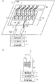
図1は、本実施形態に係るボンディングワイヤ劣化検出装置の構成及び接続を示す図であり、図1(a)はブロック図、図1(b)は回路図である。
[First Embodiment]
[Configuration of bonding wire deterioration detection device]
1A and 1B are diagrams showing the configuration and connection of a bonding wire deterioration detection apparatus according to the present embodiment. FIG. 1A is a block diagram and FIG. 1B is a circuit diagram.
図1に示すように、本実施形態に係るボンディングワイヤ劣化検出装置1は、インバータ等に搭載された基板3に接続されている。
As shown in FIG. 1, the bonding wire deterioration detection apparatus 1 according to the present embodiment is connected to a
基板3は、インバータのパワーモジュール等を構成するIGBTのチップ5が実装され、エミッタ電極Ebと、コレクタ電極Cbと、ケルビンエミッタ電極KEbとを備えている。
The
チップ5は、基板3上に実装されたIGBT等の半導体素子であり、ゲート電極Gと、コレクタ電極Cと、エミッタ電極Eと、ケルビンエミッタ電極KEとを備えている。尚、ケルビンエミッタ電極KEは、エミッタ電極Eに接続されており、同一電位となっている。また、コレクタ電極Cはチップ5の裏面に形成されている。
The
ここで、基板3のエミッタ電極Ebとチップ5のエミッタ電極Eとの間は複数のエミッタ信号用ボンディングワイヤ7で接続され、チップ5のケルビンエミッタ電極KEと基板3のケルビンエミッタ電極KEbとの間はボンディングワイヤ9で接続されている。したがって、基板3のケルビンエミッタ電極KEbは、チップ5のケルビンエミッタ電極KEと同一電位であり、これによってチップ5のエミッタ電極Eとも同一電位となる。
Here, the emitter electrode Eb of the
このような構成の基板3とチップ5に対して、本実施形態に係るボンディングワイヤ劣化検出装置1は、検査用電極Tと、電圧検出部11と、劣化検出部13とを備えている。
For the
検査用電極Tは、基板3上に設置された電極であり、複数のエミッタ信号用ボンディングワイヤ7のうちの1本のエミッタ信号用ボンディングワイヤ7Tを、エミッタ電極Eからエミッタ電極Ebとは反対方向に延長して接続されている。したがって、正常時には、検査用電極Tの電位は、エミッタ電極Eと同一になっている。また、エミッタ信号用ボンディングワイヤ7Tは、複数あるエミッタ信号用ボンディングワイヤ7のうちチップ5の中央付近に接続されていることが好ましい。これは、チップ5の中央付近は高温になるので、熱ひずみ応力でワイヤが剥離する可能性が高いためである。
The inspection electrode T is an electrode installed on the
電圧検出部11は、基板3のケルビンエミッタ電極KEbと検査用電極Tに接続され、ケルビンエミッタ電極KEbと検査用電極Tとの間の電圧Vtを検出する。
The
劣化検出部13は、電圧検出部11で検出されたケルビンエミッタ電極KEbと検査用電極Tとの間の電圧VTを監視して、エミッタ信号用ボンディングワイヤ7Tの劣化を検出する。具体的には、予め設定された所定の閾値と電圧VTを比較して、電圧VTが閾値を超えていた場合には、エミッタ信号用ボンディングワイヤ7Tに剥離等の劣化が発生したと判定する。
The
尚、ボンディングワイヤ劣化検出装置1は、例えば基板3上に実装されており、マイクロコンピュータ、マイクロプロセッサ、CPUを含む汎用の電子回路と周辺機器から構成されている。そして、特定のプログラムを実行することにより、電圧検出部11及び劣化検出部13として動作する。
The bonding wire deterioration detection device 1 is mounted on, for example, a
[ボンディングワイヤの劣化検出処理の手順]
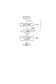
次に、本実施形態に係るボンディングワイヤ劣化検出装置1によるボンディングワイヤの劣化検出処理の手順を、図2のフローチャートを参照して説明する。
[Bonding wire degradation detection procedure]
Next, the procedure of the bonding wire deterioration detection process by the bonding wire deterioration detection apparatus 1 according to the present embodiment will be described with reference to the flowchart of FIG.
図2に示すように、ステップS10において、電圧検出部11は、チップ5のスイッチがONのときに、チップ5のケルビンエミッタ電極KEに接続されている基板3のケルビンエミッタ電極KEbと検査用電極Tとの間の電圧VTを検出する。
As shown in FIG. 2, in step S <b> 10, when the switch of the
次に、ステップS20において、劣化検出部13は、電圧検出部11で検出された電圧VTを所定の閾値と比較して監視する。
Next, in step S20, the
ここで、エミッタ信号用ボンディングワイヤ7Tが正常な状態では、検査用電極Tはチップ5のエミッタ電極Eと同じ電位である。一方、基板3のケルビンエミッタ電極KEbもエミッタ電極Eと同じ電位である。したがって、ケルビンエミッタ電極KEb(=KE=E)と検査用電極Tとの間の電位差である電圧VTは0Vとなる。この際、エミッタ信号用ボンディングワイヤ7Tには抵抗があるものの電流がほとんど流れないので、電圧降下は0となる。
Here, when the emitter signal bonding
一方、図1のPの位置でエミッタ信号用ボンディングワイヤ7Tがエミッタ電極Eから剥離すると、検査用電極Tの電圧は基板3のエミッタ電極Ebと同一の電圧となる。このとき複数のエミッタ信号用ボンディングワイヤ7には大電流が流れているので、検査用電極Tとケルビンエミッタ電極KEbとの間には電圧降下が発生する。
On the other hand, when the emitter
例えば、エミッタ信号用ボンディングワイヤ7が10本あり、250Aの電流が流れている場合に、チップ5の電圧降下は1.6V、10本のエミッタ信号用ボンディングワイヤ7の電圧降下は0.6Vとなる。この場合に1本のボンディングワイヤが剥離すると、抵抗は10/9倍になるので、検査用電極Tの電圧VT、すなわちケルビンエミッタ電極KEb(=KE=E)と検査用電極Tとの間の電位差は、0.6×(10/9)≒0.67によって0.67Vとなる。
For example, when there are 10 emitter
したがって、エミッタ信号用ボンディングワイヤ7Tが剥離する前後で、電圧VTは0Vから0.67Vへと変化する。そこで、所定の閾値として0〜0.67Vの間の値を設定しておけば、エミッタ信号用ボンディングワイヤ7Tに剥離等の劣化が発生していることを検出することができる。
Therefore, the voltage VT changes from 0V to 0.67V before and after the emitter
このようにして劣化検出部13は、所定の閾値と電圧VTとを比較して、電圧VTが閾値以下の場合にはステップS10に戻り、電圧VTが閾値を超えた場合にはステップS30に進む。
In this way, the
ステップS30では、劣化検出部13が、エミッタ信号用ボンディングワイヤ7に劣化が検出されたと判定して、本実施形態に係るボンディングワイヤの劣化検出処理を終了する。
In step S30, the
[第1実施形態の効果]
次に、本実施形態に係るボンディングワイヤ劣化検出装置1による効果を説明する。上述したように、本実施形態に係るボンディングワイヤ劣化検出装置1では、エミッタ信号用ボンディングワイヤ7Tが剥離する前後で、電圧VTは0Vから0.67Vへと変化する。
[Effect of the first embodiment]
Next, effects of the bonding wire deterioration detection apparatus 1 according to the present embodiment will be described. As described above, in the bonding wire deterioration detection apparatus 1 according to this embodiment, the voltage VT changes from 0V to 0.67V before and after the emitter
これに対して、従来の特許文献1では、IGBTの電圧Vceが1.6Vで電流Icが250Aの場合に、ボンディングワイヤが剥離する前後で、電圧Vceは1.6Vから1.67Vへと変化する。 On the other hand, in the conventional patent document 1, when the IGBT voltage Vce is 1.6 V and the current Ic is 250 A, the voltage Vce changes from 1.6 V to 1.67 V before and after the bonding wire is peeled off. To do.
また、基板のエミッタ電極と基板のケルビンエミッタ電極との間の電圧を測定してボンディングワイヤの剥離を検出する従来技術では、ボンディングワイヤが剥離する前後で、電圧は0.6Vから0.67Vへと変化する。 Also, in the conventional technique for detecting the peeling of the bonding wire by measuring the voltage between the emitter electrode of the substrate and the Kelvin emitter electrode of the substrate, the voltage is changed from 0.6 V to 0.67 V before and after the bonding wire is peeled off. And change.
したがって、いずれの従来技術と比較しても、本実施形態のボンディングワイヤ劣化検出装置1のほうが正常時と劣化時との間の変動幅が大きくなるので、容易にボンディングワイヤの劣化を検出できることが分かる。特に、本実施形態では、0Vからの変化を検出できるので、ボンディングワイヤの劣化をより確実に検出することができる。 Therefore, compared with any prior art, the bonding wire deterioration detection device 1 of the present embodiment has a larger fluctuation range between the normal time and the deterioration time, so that the deterioration of the bonding wire can be easily detected. I understand. In particular, in this embodiment, since a change from 0 V can be detected, it is possible to more reliably detect deterioration of the bonding wire.
以上詳細に説明したように、本実施形態に係るボンディングワイヤ劣化検出装置1では、エミッタ信号用ボンディングワイヤ7Tを検査用電極Tに接続し、チップ5のケルビンエミッタ電極KEを基板3のケルビンエミッタ電極KEbに接続する。そして、検査用電極Tと基板3のケルビンエミッタ電極KEbとの間の電圧VTを検出して監視することでエミッタ信号用ボンディングワイヤの劣化を検出する。これにより、検出された電圧VTは正常時と劣化時との間で変動幅が大きくなるので、容易にボンディングワイヤの劣化を検出することができる。
As described above in detail, in the bonding wire deterioration detection apparatus 1 according to the present embodiment, the emitter
[第2実施形態]
次に、本発明の第2実施形態に係るボンディングワイヤ劣化検出装置について図面を参照して説明する。尚、第1実施形態と同一の構成要素には同一の番号を付して詳細な説明は省略する。
[Second Embodiment]
Next, a bonding wire deterioration detection apparatus according to a second embodiment of the present invention will be described with reference to the drawings. In addition, the same number is attached | subjected to the component same as 1st Embodiment, and detailed description is abbreviate | omitted.
[ボンディングワイヤ劣化検出装置の構成]
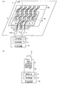
図3は、本実施形態に係るボンディングワイヤ劣化検出装置の構成及び接続を示す図であり、図3(a)はブロック図、図3(b)は回路図である。
[Configuration of bonding wire deterioration detection device]
3A and 3B are diagrams showing the configuration and connection of the bonding wire deterioration detection apparatus according to the present embodiment. FIG. 3A is a block diagram and FIG. 3B is a circuit diagram.
図3に示すように、本実施形態では、検査用電極Tに複数のエミッタ信号用ボンディングワイヤが接続されていることが第1実施形態と相違している。図3では、10本あるエミッタ信号用ボンディングワイヤ7のうち、4本のエミッタ信号用ボンディングワイヤ7Ta〜7Tdが検査用電極Tに接続されている。
As shown in FIG. 3, the present embodiment is different from the first embodiment in that a plurality of emitter signal bonding wires are connected to the inspection electrode T. In FIG. 3, four emitter signal bonding wires 7Ta to 7Td among the ten emitter
通常、IGBTのチップ5に通電すると、図3のAに示すチップ5の中央付近の領域が高温になるため、ボンディングワイヤはチップ5の中央付近から先に剥離していく。そこで、チップ5の中央付近に接続されている複数のエミッタ信号用ボンディングワイヤ7Ta〜7Tdを検査用電極Tに接続しておくことによって、劣化の起こりやすい領域を監視することが可能となる。また、複数のエミッタ信号用ボンディングワイヤ7Ta〜7Tdを同時に監視することも可能となる。
Normally, when the
[第2実施形態の効果]
次に、本実施形態に係るボンディングワイヤ劣化検出装置31による効果を説明する。本実施形態に係るボンディングワイヤ劣化検出装置31では、エミッタ信号用ボンディングワイヤ7Ta〜7Tdのうちの1本が剥離すると、検査用電極Tの電位は基板3のエミッタ電極Ebとチップ5のエミッタ電極Eとの間の電圧となる。このとき、剥離した1本のボンディングワイヤと剥離していない3本のボンディングワイヤとの間の抵抗分圧が6:1とすると、検査用電極Tの電位は、0.67×(1/7)≒0.10によってエミッタ電極Eより0.10V低くなる。したがって、電圧VTは、エミッタ信号用ボンディングワイヤ7Ta〜7Tdのうちの1本が剥離する前後で、0Vから0.10Vへと変化する。
[Effects of Second Embodiment]
Next, effects of the bonding wire
これに対して、従来の特許文献1では、第1実施形態で説明したようにボンディングワイヤが剥離する前後で電圧Vceは1.6Vから1.67Vへと変化する。また、基板のエミッタ電極と基板のケルビンエミッタ電極との間の電圧を測定してボンディングワイヤの剥離を検出する従来技術では、ボンディングワイヤが剥離する前後で、電圧は0.6Vから0.67Vへと変化する。 On the other hand, in the conventional patent document 1, as described in the first embodiment, the voltage Vce changes from 1.6V to 1.67V before and after the bonding wire is peeled off. Also, in the conventional technique for detecting the peeling of the bonding wire by measuring the voltage between the emitter electrode of the substrate and the Kelvin emitter electrode of the substrate, the voltage is changed from 0.6 V to 0.67 V before and after the bonding wire is peeled off. And change.
したがって、いずれの従来技術と比較しても、本実施形態のボンディングワイヤ劣化検出装置31のほうが正常時と劣化時との間の変動幅が大きくなるので、容易にボンディングワイヤの劣化を検出できることが分かる。特に、本実施形態では、0Vからの変化を検出できるので、ボンディングワイヤの劣化をより確実に検出することができる。
Therefore, as compared with any conventional technique, the bonding wire
以上詳細に説明したように、本実施形態に係るボンディングワイヤ劣化検出装置31では、検査用電極Tに複数のエミッタ信号用ボンディングワイヤ7Ta〜7Tdを接続する。これにより、複数のボンディングワイヤが接続されているチップ5の広い領域を同時に監視することができる。
As described above in detail, in the bonding wire
また、本実施形態に係るボンディングワイヤ劣化検出装置31では、複数あるエミッタ信号用ボンディングワイヤ7のうちチップ5の中央付近に接続されているエミッタ信号用ボンディングワイヤ7Ta〜7Tdを検査用電極Tに接続する。これにより、高温になって劣化の起こりやすいチップ5の中央付近の領域を監視することができる。
In the bonding wire
なお、上述の実施形態は本発明の一例である。このため、本発明は、上述の実施形態に限定されることはなく、この実施形態以外の形態であっても、本発明に係る技術的思想を逸脱しない範囲であれば、設計などに応じて種々の変更が可能であることは勿論である。 The above-described embodiment is an example of the present invention. For this reason, the present invention is not limited to the above-described embodiment, and even if it is a form other than this embodiment, as long as it does not depart from the technical idea of the present invention, it depends on the design and the like. Of course, various modifications are possible.
1、31 ボンディングワイヤ劣化検出装置
3 基板
5 チップ
7、7T、7Ta〜7Td エミッタ信号用ボンディングワイヤ
9 ボンディングワイヤ
C、Cb コレクタ電極
E、Eb エミッタ電極
G ゲート電極
KE、KEb ケルビンエミッタ電極
T 検査用電極
11 電圧検出部
13 劣化検出部
DESCRIPTION OF
Claims (4)
前記基板(3)のエミッタ電極(Eb)と前記半導体素子(5)のエミッタ電極(E)とを接続するエミッタ信号用ボンディングワイヤ(7T)を、前記半導体素子(5)のエミッタ電極(E)から前記基板(3)のエミッタ電極(Eb)とは反対方向に延長して接続された検査用電極(T)と、
前記半導体素子(5)のケルビンエミッタ電極(KE)に接続された前記基板(3)のケルビンエミッタ電極(KEb)と前記検査用電極(T)との間の電圧を検出する電圧検出手段(11)と、
前記電圧検出手段(11)によって検出された前記基板(3)のケルビンエミッタ電極(KEb)と前記検査用電極(T)との間の電圧を監視して、前記エミッタ信号用ボンディングワイヤ(7T)の劣化を検出する劣化検出手段(13)と
を備えたことを特徴とするボンディングワイヤ劣化検出装置。 In a bonding wire deterioration detecting device (1) for detecting deterioration of a bonding wire connecting a substrate (3) and a semiconductor element (5) mounted on the substrate (3),
An emitter signal bonding wire (7T) connecting the emitter electrode (Eb) of the substrate (3) and the emitter electrode (E) of the semiconductor element (5) is connected to the emitter electrode (E) of the semiconductor element (5). An inspection electrode (T) connected in an extending direction from the emitter electrode (Eb) of the substrate (3) to the opposite direction;
Voltage detecting means (11) for detecting a voltage between the Kelvin emitter electrode (KEb) of the substrate (3) connected to the Kelvin emitter electrode (KE) of the semiconductor element (5) and the inspection electrode (T). )When,
The voltage between the Kelvin emitter electrode (KEb) of the substrate (3) and the inspection electrode (T) detected by the voltage detection means (11) is monitored, and the emitter signal bonding wire (7T) A bonding wire deterioration detecting device comprising deterioration detecting means (13) for detecting deterioration of the wire.
前記基板(3)のエミッタ電極(Eb)と前記半導体素子(5)のエミッタ電極(E)とを接続するエミッタ信号用ボンディングワイヤ(7T)を、前記半導体素子(5)のエミッタ電極(E)から前記基板(3)のエミッタ電極(Eb)とは反対方向に延長して接続された検査用電極(T)と、前記半導体素子(5)のケルビンエミッタ電極(KE)に接続された前記基板(3)のケルビンエミッタ電極(KEb)との間の電圧を検出する電圧検出ステップと、
前記電圧検出ステップで検出された前記基板(3)のケルビンエミッタ電極(KEb)と前記検査用電極(T)との間の電圧を監視して、前記エミッタ信号用ボンディングワイヤ(7T)の劣化を検出する劣化検出ステップと
を含むことを特徴とするボンディングワイヤ劣化検出方法。 In a bonding wire deterioration detection method for detecting deterioration of a bonding wire connecting a substrate (3) and a semiconductor element (5) mounted on the substrate (3),
An emitter signal bonding wire (7T) connecting the emitter electrode (Eb) of the substrate (3) and the emitter electrode (E) of the semiconductor element (5) is connected to the emitter electrode (E) of the semiconductor element (5). The inspection electrode (T) connected to extend in the opposite direction to the emitter electrode (Eb) of the substrate (3) and the substrate connected to the Kelvin emitter electrode (KE) of the semiconductor element (5) (3) a voltage detection step of detecting a voltage between the Kelvin emitter electrode (KEb);
By monitoring the voltage between the Kelvin emitter electrode (KEb) of the substrate (3) and the inspection electrode (T) detected in the voltage detection step, the emitter signal bonding wire (7T) is deteriorated. A bonding wire deterioration detection method, comprising: a deterioration detection step of detecting.
Priority Applications (1)
| Application Number | Priority Date | Filing Date | Title |
|---|---|---|---|
| JP2013254932A JP2015114149A (en) | 2013-12-10 | 2013-12-10 | Device and method for detecting deterioration of bonding wire |
Applications Claiming Priority (1)
| Application Number | Priority Date | Filing Date | Title |
|---|---|---|---|
| JP2013254932A JP2015114149A (en) | 2013-12-10 | 2013-12-10 | Device and method for detecting deterioration of bonding wire |
Publications (1)
| Publication Number | Publication Date |
|---|---|
| JP2015114149A true JP2015114149A (en) | 2015-06-22 |
Family
ID=53528081
Family Applications (1)
| Application Number | Title | Priority Date | Filing Date |
|---|---|---|---|
| JP2013254932A Pending JP2015114149A (en) | 2013-12-10 | 2013-12-10 | Device and method for detecting deterioration of bonding wire |
Country Status (1)
| Country | Link |
|---|---|
| JP (1) | JP2015114149A (en) |
Cited By (4)
| Publication number | Priority date | Publication date | Assignee | Title |
|---|---|---|---|---|
| WO2019146258A1 (en) * | 2018-01-26 | 2019-08-01 | 三菱電機株式会社 | Semiconductor device and power conversion device |
| JPWO2021176695A1 (en) * | 2020-03-06 | 2021-09-10 | ||
| CN113994467A (en) * | 2019-06-25 | 2022-01-28 | 三菱电机株式会社 | Semiconductor device and power conversion device |
| JP2023056305A (en) * | 2021-10-07 | 2023-04-19 | 富士電機株式会社 | Power conversion device and deterioration determination method |
-
2013
- 2013-12-10 JP JP2013254932A patent/JP2015114149A/en active Pending
Cited By (8)
| Publication number | Priority date | Publication date | Assignee | Title |
|---|---|---|---|---|
| WO2019146258A1 (en) * | 2018-01-26 | 2019-08-01 | 三菱電機株式会社 | Semiconductor device and power conversion device |
| US11677312B2 (en) | 2018-01-26 | 2023-06-13 | Mitsubishi Electric Corporation | Semiconductor device and power converter |
| CN113994467A (en) * | 2019-06-25 | 2022-01-28 | 三菱电机株式会社 | Semiconductor device and power conversion device |
| JPWO2021176695A1 (en) * | 2020-03-06 | 2021-09-10 | ||
| WO2021176695A1 (en) * | 2020-03-06 | 2021-09-10 | 三菱電機株式会社 | Semiconductor device and power conversion device |
| CN115210868A (en) * | 2020-03-06 | 2022-10-18 | 三菱电机株式会社 | Semiconductor device and power conversion device |
| JP7286002B2 (en) | 2020-03-06 | 2023-06-02 | 三菱電機株式会社 | Semiconductor equipment and power conversion equipment |
| JP2023056305A (en) * | 2021-10-07 | 2023-04-19 | 富士電機株式会社 | Power conversion device and deterioration determination method |
Similar Documents
| Publication | Publication Date | Title |
|---|---|---|
| JP5233198B2 (en) | Semiconductor device | |
| TWI344682B (en) | Semiconductor device having function for detecting defect | |
| US20180284181A1 (en) | On-line health management device and method for insulated gate bipolar transistor | |
| JP2022516387A5 (en) | ||
| JP2015114149A (en) | Device and method for detecting deterioration of bonding wire | |
| JP5343555B2 (en) | Semiconductor device and method for detecting destruction of solder joint | |
| JP2014228330A (en) | Solder crack detection device and solder crack detection method | |
| JP4581930B2 (en) | Anomaly detection device for power semiconductor elements | |
| JP2014236538A (en) | Solder deterioration detection device and solder deterioration detection method | |
| US9664728B2 (en) | Detection of defective electrical connections | |
| US20160146878A1 (en) | Electronic Assembly for Prognostics of Solder Joint | |
| JP4967924B2 (en) | Semiconductor device | |
| JP2010281625A (en) | Inspection method of semiconductor chip | |
| JP5151320B2 (en) | Power semiconductor device | |
| CN109307826B (en) | Insulation inspection device and insulation inspection method | |
| JP2013247244A (en) | Electronic device, breakage estimation method and life estimation method | |
| JP2008251716A (en) | Semiconductor device and inspection method thereof | |
| JP5326898B2 (en) | External terminal open / short circuit inspection method in integrated circuit and external terminal open / short circuit inspection apparatus in integrated circuit | |
| JP5370250B2 (en) | Manufacturing method of semiconductor device | |
| JP2013225535A (en) | Semiconductor device and semiconductor testing device | |
| JP2010038639A (en) | Reliability evaluation method of semiconductor device, and reliability evaluation device of semiconductor device | |
| JP2012037411A (en) | Semiconductor device inspection method and inspection apparatus | |
| JP7497629B2 (en) | Semiconductor chip testing device and testing method | |
| JP6652337B2 (en) | Method of inspecting mounting state of semiconductor device and semiconductor device mounted on mounting substrate | |
| JP6862278B2 (en) | Inspection system |