JP2015102403A - Package, electronic component mounting package, physical quantity sensor, electronic equipment and mobile object - Google Patents
Package, electronic component mounting package, physical quantity sensor, electronic equipment and mobile object Download PDFInfo
- Publication number
- JP2015102403A JP2015102403A JP2013242556A JP2013242556A JP2015102403A JP 2015102403 A JP2015102403 A JP 2015102403A JP 2013242556 A JP2013242556 A JP 2013242556A JP 2013242556 A JP2013242556 A JP 2013242556A JP 2015102403 A JP2015102403 A JP 2015102403A
- Authority
- JP
- Japan
- Prior art keywords
- wiring
- base
- substrate
- terminal
- outer edge
- Prior art date
- Legal status (The legal status is an assumption and is not a legal conclusion. Google has not performed a legal analysis and makes no representation as to the accuracy of the status listed.)
- Granted
Links
Images
Classifications
-
- G—PHYSICS
- G01—MEASURING; TESTING
- G01C—MEASURING DISTANCES, LEVELS OR BEARINGS; SURVEYING; NAVIGATION; GYROSCOPIC INSTRUMENTS; PHOTOGRAMMETRY OR VIDEOGRAMMETRY
- G01C19/00—Gyroscopes; Turn-sensitive devices using vibrating masses; Turn-sensitive devices without moving masses; Measuring angular rate using gyroscopic effects
- G01C19/56—Turn-sensitive devices using vibrating masses, e.g. vibratory angular rate sensors based on Coriolis forces
- G01C19/5607—Turn-sensitive devices using vibrating masses, e.g. vibratory angular rate sensors based on Coriolis forces using vibrating tuning forks
- G01C19/5628—Manufacturing; Trimming; Mounting; Housings
-
- G—PHYSICS
- G01—MEASURING; TESTING
- G01C—MEASURING DISTANCES, LEVELS OR BEARINGS; SURVEYING; NAVIGATION; GYROSCOPIC INSTRUMENTS; PHOTOGRAMMETRY OR VIDEOGRAMMETRY
- G01C19/00—Gyroscopes; Turn-sensitive devices using vibrating masses; Turn-sensitive devices without moving masses; Measuring angular rate using gyroscopic effects
- G01C19/56—Turn-sensitive devices using vibrating masses, e.g. vibratory angular rate sensors based on Coriolis forces
- G01C19/5607—Turn-sensitive devices using vibrating masses, e.g. vibratory angular rate sensors based on Coriolis forces using vibrating tuning forks
- G01C19/5621—Turn-sensitive devices using vibrating masses, e.g. vibratory angular rate sensors based on Coriolis forces using vibrating tuning forks the devices involving a micromechanical structure
-
- H—ELECTRICITY
- H10—SEMICONDUCTOR DEVICES; ELECTRIC SOLID-STATE DEVICES NOT OTHERWISE PROVIDED FOR
- H10W—GENERIC PACKAGES, INTERCONNECTIONS, CONNECTORS OR OTHER CONSTRUCTIONAL DETAILS OF DEVICES COVERED BY CLASS H10
- H10W72/00—Interconnections or connectors in packages
- H10W72/50—Bond wires
- H10W72/541—Dispositions of bond wires
- H10W72/5445—Dispositions of bond wires being orthogonal to a side surface of the chip, e.g. parallel arrangements
-
- H—ELECTRICITY
- H10—SEMICONDUCTOR DEVICES; ELECTRIC SOLID-STATE DEVICES NOT OTHERWISE PROVIDED FOR
- H10W—GENERIC PACKAGES, INTERCONNECTIONS, CONNECTORS OR OTHER CONSTRUCTIONAL DETAILS OF DEVICES COVERED BY CLASS H10
- H10W72/00—Interconnections or connectors in packages
- H10W72/90—Bond pads, in general
- H10W72/931—Shapes of bond pads
- H10W72/932—Plan-view shape, i.e. in top view
Landscapes
- Engineering & Computer Science (AREA)
- Physics & Mathematics (AREA)
- General Physics & Mathematics (AREA)
- Radar, Positioning & Navigation (AREA)
- Remote Sensing (AREA)
- Manufacturing & Machinery (AREA)
- Gyroscopes (AREA)
Abstract
Description
本発明は、パッケージ、電子部品搭載パッケージ、物理量センサー、電子機器および移動体に関する。 The present invention relates to a package, an electronic component mounting package, a physical quantity sensor, an electronic device, and a moving object.
従来から、角速度などの物理量を検出するための物理量センサーとして、特許文献1のような角速度センサーが知られている。
特許文献1に記載の角速度センサーは、パッケージと、パッケージに収容されている振ジャイロ素子およびICと、を有している。また、パッケージ(ベース)には複数の配線が形成されており、当該配線を介して、ICの所定の端子がジャイロ素子と電気的に接続されていたり、外部へ引き出されていたりする。より具体的には、複数の配線には、少なくとも、ジャイロ素子が有する第1の検出端子と電気的に接続されている第1検出配線と、第2の検出端子と電気的に接続されている第2検出配線と、ICへ信号を入力したり、ICから信号が出力されたりする入出力配線と、が含まれている。
Conventionally, as a physical quantity sensor for detecting a physical quantity such as an angular speed, an angular speed sensor as in Patent Document 1 is known.
The angular velocity sensor described in Patent Document 1 includes a package, and a vibrating gyro element and an IC housed in the package. In addition, a plurality of wirings are formed in the package (base), and predetermined terminals of the IC are electrically connected to the gyro element or drawn out through the wirings. More specifically, the plurality of wirings are electrically connected to at least a first detection wiring electrically connected to a first detection terminal included in the gyro element and a second detection terminal. A second detection wiring and an input / output wiring for inputting a signal to the IC and outputting a signal from the IC are included.
近年、ICと外部との信号を入出力する手段としてデジタルインタフェースが用いられることが増えている。デジタルインタフェースを用いる場合、前述した複数の配線には、ICへデジタル信号を入力したり、ICからデジタル信号が出力されたりする入出力配線が含まれている。そのため、第1および第2検出配線(第1、第2の検出信号入力パッド)と入出力配線(入出力パッド)との間の電気的な結合により、ノイズが第1、第2検出配線に混入し、検出信号を正確に取得することができない場合がある。
本発明は、ノイズ干渉を低減することのできるパッケージ、電子部品搭載パッケージ、物理量センサー、電子機器および移動体を提供することを目的とする。
In recent years, digital interfaces are increasingly used as means for inputting and outputting signals between an IC and the outside. In the case of using a digital interface, the plurality of wirings described above include input / output wirings for inputting digital signals to the IC and outputting digital signals from the IC. Therefore, noise is generated in the first and second detection wirings due to electrical coupling between the first and second detection wirings (first and second detection signal input pads) and the input / output wirings (input / output pads). In some cases, the detection signal cannot be obtained accurately.
An object of this invention is to provide the package which can reduce noise interference, an electronic component mounting package, a physical quantity sensor, an electronic device, and a moving body.
このような目的は、下記の本発明により達成される。
[適用例1]
本適用例のパッケージは、電子部品が配置されるベースと、
前記ベースに配置されている複数の配線と、
を有し、
前記配線は、
前記電子部品と接続される内部端子を有する複数の第1の配線と、
前記電子部品と接続される内部端子を有する複数の第2の配線と、
を有し、
前記複数の第1の配線の前記内部端子は、第1の軸に沿って並んで配置され、
前記複数の第2の配線の前記内部端子は、前記第1の軸に交差する第2の軸に沿って並んで配置され、
前記第2の配線は、前記物理量検出素子の検出電極に電気的に接続される検出信号配線を含み、
前記複数の第1の配線は、デジタル信号を伝送するデジタル信号配線を含み、
前記デジタル信号配線の内部端子は、前記複数の第1の配線の前記複数の内部端子における前記第1の軸方向の中央線に対して、前記第2の軸と反対側に配置されていることを特徴とする。
これにより、第1の配線と第2の配線とを離間させることができるため、第1の配線から第2の配線へのノイズ干渉を低減することができる。
Such an object is achieved by the present invention described below.
[Application Example 1]
The package of this application example includes a base on which electronic components are arranged,
A plurality of wires arranged on the base;
Have
The wiring is
A plurality of first wires having internal terminals connected to the electronic component;
A plurality of second wires having internal terminals connected to the electronic component;
Have
The internal terminals of the plurality of first wires are arranged side by side along a first axis,
The internal terminals of the plurality of second wires are arranged side by side along a second axis that intersects the first axis,
The second wiring includes a detection signal wiring electrically connected to a detection electrode of the physical quantity detection element,
The plurality of first wirings include digital signal wirings for transmitting digital signals,
The internal terminal of the digital signal wiring is disposed on the side opposite to the second axis with respect to the center line in the first axial direction of the plurality of internal terminals of the plurality of first wirings. It is characterized by.
As a result, the first wiring and the second wiring can be separated from each other, so that noise interference from the first wiring to the second wiring can be reduced.
[適用例2]
本適用例のパッケージは、電子部品が配置されるベースと、
前記ベースに配置されている配線と、
を有し、
前記ベースは、前記ベースの平面視にて、
第1の外縁と、
前記第1の外縁の一端側に位置し、前記第1の外縁と交差する方向に延在する第2の外縁と、
を有し、
前記配線は、
前記電子部品に接続される内部端子、および前記ベースの前記第1の外縁に対応する側面に配置されている側面電極、を有する第1の配線と、
前記第2の外縁に平行な軸に沿って並んで配置され、前記電子部品と接続される内部端子を有する複数の第2の配線と、
を有し、
前記第1の配線は、デジタル信号を伝送するデジタル信号配線を含み、
前記第2の配線は、前記物理量検出素子の検出電極に電気的に接続される検出信号配線を含むことを特徴とする。
これにより、第1の配線と第2の配線とを離間させることができるため、第1の配線から第2の配線へのノイズ干渉を低減することができる。
[Application Example 2]
The package of this application example includes a base on which electronic components are arranged,
Wiring arranged on the base;
Have
The base is a plan view of the base,
A first outer edge;
A second outer edge located on one end side of the first outer edge and extending in a direction intersecting the first outer edge;
Have
The wiring is
A first wiring having an internal terminal connected to the electronic component and a side electrode disposed on a side surface corresponding to the first outer edge of the base;
A plurality of second wirings arranged along an axis parallel to the second outer edge and having an internal terminal connected to the electronic component;
Have
The first wiring includes a digital signal wiring for transmitting a digital signal;
The second wiring includes a detection signal wiring electrically connected to a detection electrode of the physical quantity detection element.
As a result, the first wiring and the second wiring can be separated from each other, so that noise interference from the first wiring to the second wiring can be reduced.
[適用例3]
本適用例のパッケージでは、前記第1の配線は、複数であり、
前記第1の配線の前記内部端子は、前記第1の外縁に平行な軸に沿って並んで配置されていることが好ましい。
これにより、第1の配線の内部端子と第2の配線の内部端子とを離間させることができ、第1の配線から第2の配線へのノイズ干渉が低減される。
[Application Example 3]
In the package of this application example, the first wiring is plural,
The internal terminals of the first wiring are preferably arranged side by side along an axis parallel to the first outer edge.
Thereby, the internal terminal of the 1st wiring and the internal terminal of the 2nd wiring can be separated, and noise interference from the 1st wiring to the 2nd wiring is reduced.
[適用例4]
本適用例のパッケージでは、前記デジタル信号配線の前記内部端子と前記検出信号配線の前記内部端子との間に、接地配線および電位が固定されている固定電位配線の少なくとも一方が配置されていることが好ましい。
これにより、接地配線または固定電位配線がシールド層として機能するため、第1の配線から第2の配線へのノイズ干渉がより低減される。
[Application Example 4]
In the package of this application example, at least one of the ground wiring and the fixed potential wiring in which the potential is fixed is disposed between the internal terminal of the digital signal wiring and the internal terminal of the detection signal wiring. Is preferred.
Thereby, since the ground wiring or the fixed potential wiring functions as a shield layer, noise interference from the first wiring to the second wiring is further reduced.
[適用例5]
本適用例のパッケージは、電子部品が配置されるベースと、
前記ベースに配置されている複数の配線と、
を有し、
前記複数の配線は、
前記電子部品と接続される内部端子を有する複数の第1の配線と、
前記電子部品と接続される内部端子を有する第2の配線と、
を有し、
前記複数の第1の配線は、デジタル信号を伝送するデジタル信号配線を含み、
前記第2の配線は、前記物理量検出素子の検出電極に電気的に接続される検出信号配線を含み、
前記デジタル信号配線と前記検出信号配線との間に、接地配線または電位が固定されている固定電位配線が配置されていることを特徴とする。
これにより、接地配線または固定電位配線がシールド層として機能するため、第1の配線から第2の配線へのノイズ干渉が低減される。
[Application Example 5]
The package of this application example includes a base on which electronic components are arranged,
A plurality of wires arranged on the base;
Have
The plurality of wirings are
A plurality of first wires having internal terminals connected to the electronic component;
A second wiring having an internal terminal connected to the electronic component;
Have
The plurality of first wirings include digital signal wirings for transmitting digital signals,
The second wiring includes a detection signal wiring electrically connected to a detection electrode of the physical quantity detection element,
Between the digital signal wiring and the detection signal wiring, a ground wiring or a fixed potential wiring with a fixed potential is arranged.
Thereby, since the ground wiring or the fixed potential wiring functions as a shield layer, noise interference from the first wiring to the second wiring is reduced.
[適用例6]
本適用例のパッケージでは、前記ベースは、前記ベースの平面視にて、
第1の外縁と、
前記第1の外縁の一端側に位置し、前記第1の外縁と交差する方向に延在する第2の外縁と、
を有し、
前記複数の第1の配線の内部端子は、前記第1の外縁と平行な第1の軸に沿って配置され、
前記第2の配線は、複数であり、
前記複数の第2の配線の内部端子は、前記第2の外縁と平行な第2の軸に沿って配置されていることが好ましい。
これにより、第1の配線と第2の配線とを離間させることができ、第1の配線から第2の配線へのノイズ干渉がより低減される。
[Application Example 6]
In the package of this application example, the base is a plan view of the base,
A first outer edge;
A second outer edge located on one end side of the first outer edge and extending in a direction intersecting the first outer edge;
Have
The internal terminals of the plurality of first wirings are disposed along a first axis parallel to the first outer edge,
The second wiring is plural,
The internal terminals of the plurality of second wires are preferably arranged along a second axis parallel to the second outer edge.
Accordingly, the first wiring and the second wiring can be separated from each other, and noise interference from the first wiring to the second wiring is further reduced.
[適用例7]
本適用例のパッケージでは、前記デジタル信号配線の内部端子は、前記第1の外縁の他端側に配置されていることが好ましい。
これにより、第1の配線と第2の配線とをより離間させることができ、第1の配線から第2の配線へのノイズ干渉がさらに低減される。
[Application Example 7]
In the package of this application example, it is preferable that an internal terminal of the digital signal wiring is disposed on the other end side of the first outer edge.
Thereby, the first wiring and the second wiring can be further separated, and noise interference from the first wiring to the second wiring is further reduced.
[適用例8]
本適用例の電素子搭載パッケージは、本適用例のパッケージと、
前記電子部品と、
を有することを特徴とする電子部品搭載パッケージ。
これにより、信頼性の高い電子部品搭載パッケージが得られる。
[Application Example 8]
The electric device mounting package of this application example includes the package of this application example,
The electronic component;
An electronic component mounting package characterized by comprising:
Thereby, a highly reliable electronic component mounting package is obtained.
[適用例9]
本適用例の電子部品搭載パッケージは、ベースと、
前記ベースに配置された電子部品と、
前記電子部品と接続される第1の配線と、
前記電子部品と接続される第2の配線と、
前記電子部品と前記第1の配線とを接続する第1の導電性ワイヤーと、
前記電子部品と前記第2の配線とを接続する第2の導電性ワイヤーと、
を有し、
前記第1の配線は、デジタル信号を伝送するデジタル信号配線を含み、
前記第2の配線は、前記物理量検出素子の検出電極に電気的に接続される検出信号配線を含み、
前記ベースの平面視にて、前記デジタル信号配線に接続される前記第1の導電性ワイヤーの延在方向と、前記検出信号配線に接続される前記第2の導電性ワイヤーの延在方向とが交差していることを特徴とする。
これにより、第1の導電性ワイヤーと第2の導電性ワイヤーとを離間させることができ、第1の配線から第2の配線へのノイズ干渉が低減される。
[適用例10]
本適用例の電子部品搭載パッケージでは、前記ベースの平面視にて、前記デジタル信号配線に接続される前記第1の導電性ワイヤーの前記延在方向と、前記検出信号配線に接続される前記第2の導電性ワイヤーの前記延在方向とが直交していることが好ましい。
[Application Example 9]
The electronic component mounting package of this application example has a base,
An electronic component disposed on the base;
A first wiring connected to the electronic component;
A second wiring connected to the electronic component;
A first conductive wire connecting the electronic component and the first wiring;
A second conductive wire connecting the electronic component and the second wiring;
Have
The first wiring includes a digital signal wiring for transmitting a digital signal;
The second wiring includes a detection signal wiring electrically connected to a detection electrode of the physical quantity detection element,
An extension direction of the first conductive wire connected to the digital signal wiring and an extension direction of the second conductive wire connected to the detection signal wiring in a plan view of the base It is characterized by crossing.
Thereby, a 1st conductive wire and a 2nd conductive wire can be spaced apart, and the noise interference from a 1st wiring to a 2nd wiring is reduced.
[Application Example 10]
In the electronic component mounting package of this application example, the extending direction of the first conductive wire connected to the digital signal wiring and the first connection connected to the detection signal wiring in a plan view of the base. It is preferable that the extending direction of the two conductive wires is orthogonal.
[適用例11]
本適用例の物理量センサーは、本適用例の電子部品搭載パッケージと、
前記物理量検出素子と、
を有することを特徴とする。
これにより、信頼性の高い電子部品搭載パッケージが得られる。
[Application Example 11]
The physical quantity sensor of this application example includes the electronic component mounting package of this application example,
The physical quantity detection element;
It is characterized by having.
Thereby, a highly reliable electronic component mounting package is obtained.
[適用例11]
本適用例の電子機器は、本適用例の物理量センサーを備えていることを特徴とする。
これにより、信頼性の高い電子機器が得られる。
[適用例12]
本適用例の移動体は、本適用例の物理量センサーを備えていることを特徴とする。
これにより、信頼性の高い移動体が得られる。
[Application Example 11]
An electronic apparatus according to this application example includes the physical quantity sensor according to this application example.
As a result, a highly reliable electronic device can be obtained.
[Application Example 12]
The moving body of this application example includes the physical quantity sensor of this application example.
Thereby, a mobile body with high reliability is obtained.
以下、本発明のパッケージ、電子部品搭載パッケージ、物理量センサー、電子機器および移動体を添付図面に示す実施形態に基づいて詳細に説明する。
1.物理量センサー
<第1実施形態>
図1は、本発明の第1実施形態に係る物理量センサーの平面図(上面図)である。図2は、図1中のA−A線断面図である。図3は、図1に示す物理量センサーが有するジャイロ素子を示す平面図(上面図)である。図4は、図3に示すジャイロ素子の電極配置を示す平面図(上面図)である。図5は、図3に示すジャイロ素子の電極配置を示す平面図(上側から見た透過図)である。図6は、図3に示すジャイロ素子の動作を説明するための図である。図7は、(a)が第1基板の平面図(上側から見た透過図)、(b)が第2基板の平面図(上面図)である。図8は、(a)が第3基板の平面図(上面図)、(b)が第4基板の平面図(上面図)である。図9は、(a)が第5基板の平面図(上面図)、(b)が第6基板の平面図(上面図)である。図10は、ベースの平面図(上面図)である。図11は、図1に示す振動が有する支持基板の平面図(上面図)である。図12は、支持基板とベースの接合状態を示す平面図(上面図)である。図13は、支持基板とジャイロ素子の接合状態を示す平面図(下面図)である。なお、以下では、説明の便宜上、図1中の紙面手前側および図2中の上側を「上」とも言い、図1中の紙面奥側およびお図2中の下側を「下」とも言う。また、以下では、X軸に沿った方向を「X軸方向」とも言い、Y軸に沿った方向を「Y軸方向」とも言う。
Hereinafter, a package, an electronic component mounting package, a physical quantity sensor, an electronic device, and a moving body of the present invention will be described in detail based on embodiments shown in the accompanying drawings.
1. Physical quantity sensor <First embodiment>
FIG. 1 is a plan view (top view) of the physical quantity sensor according to the first embodiment of the present invention. 2 is a cross-sectional view taken along line AA in FIG. FIG. 3 is a plan view (top view) showing a gyro element included in the physical quantity sensor shown in FIG. FIG. 4 is a plan view (top view) showing an electrode arrangement of the gyro element shown in FIG. FIG. 5 is a plan view (transmission view seen from above) showing the electrode arrangement of the gyro element shown in FIG. FIG. 6 is a diagram for explaining the operation of the gyro element shown in FIG. 7A is a plan view of the first substrate (transparent view seen from above), and FIG. 7B is a plan view of the second substrate (top view). 8A is a plan view (top view) of the third substrate, and FIG. 8B is a plan view (top view) of the fourth substrate. 9A is a plan view (top view) of the fifth substrate, and FIG. 9B is a plan view (top view) of the sixth substrate. FIG. 10 is a plan view (top view) of the base. FIG. 11 is a plan view (top view) of the support substrate included in the vibration shown in FIG. FIG. 12 is a plan view (top view) showing a bonded state of the support substrate and the base. FIG. 13 is a plan view (bottom view) showing a bonded state of the support substrate and the gyro element. In the following, for the sake of convenience of explanation, the front side in FIG. 1 and the upper side in FIG. 2 are also referred to as “up”, and the back side in FIG. 1 and the lower side in FIG. . In the following, the direction along the X axis is also referred to as “X axis direction”, and the direction along the Y axis is also referred to as “Y axis direction”.
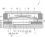
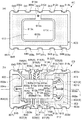
図1および図2に示す物理量センサー1は、ジャイロセンサーであって、ジャイロ素子(物理量検出素子)2と、ジャイロ素子2を収容するパッケージ5と、ジャイロ素子2を支持するとともに、パッケージ5に固定されている支持基板9と、パッケージ5内に配置されているIC(電子部品)10と、を有している。なお、IC10が搭載された状態のパッケージ5を電子部品搭載パッケージとする。
A physical quantity sensor 1 shown in FIGS. 1 and 2 is a gyro sensor, which is a gyro element (physical quantity detection element) 2, a
以下、これら各構成要素について順次説明する。
≪ジャイロ素子≫
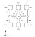
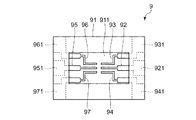
図3に示すように、ジャイロ素子2は、振動片3と、振動片3に形成された電極とを有している。
−振動片−
振動片3の構成材料としては、例えば、水晶、タンタル酸リチウム、ニオブ酸リチウムなどの圧電材料が挙げられる。これらの中でも、振動片3の構成材料としては、水晶を用いることが好ましい。水晶を用いることで、他の材料と比較して優れた周波数温度特性を有するジャイロ素子2が得られる。なお、以下では、振動片3を水晶で構成した場合について説明する。
Hereinafter, each of these components will be described sequentially.
≪Gyro element≫
As shown in FIG. 3, the
-Vibrating piece-
Examples of the constituent material of the
振動片3は、水晶基板の結晶軸であるY軸(機械軸)およびX軸(電気軸)で規定されるXY平面に広がりを有し、Z軸(光軸)方向に厚みを有する板状をなしている。すなわち、振動片3は、Zカット水晶板で構成されている。なお、Z軸は、振動片3の厚さ方向と一致しているのが好ましいが、常温近傍における周波数温度変化を小さくする観点から、厚さ方向に対して若干(例えば、−5°≦θ≦15°程度)傾けてもよい。
The
このような振動片3は、中心部に位置する基部31と、基部31からY軸方向両側に延出している第1、第2検出腕321、322と、基部31からX軸方向両側に延在している第1、第2連結腕331、332と、第1連結腕331の先端部からY軸方向両側に延出している第1、第2駆動腕341、342と、第2連結腕332の先端部からY軸方向両側に延出している第3、第4駆動腕343、344と、を有している。
Such a
第1検出腕321は、基部31から+Y軸方向に延出し、その先端部には幅広のハンマーヘッド3211が設けられている。一方、第2検出腕322は、基部31から−Y軸方向に延出し、その先端部には幅広のハンマーヘッド3221が設けられている。これら第1、第2検出腕321、322は、ジャイロ素子2の重心Gを通るXZ平面に関して面対称に配置されている。なお、ハンマーヘッド3211、3221は、必要に応じて設ければよく、省略してもよい。また、必要に応じて、第1、第2検出腕321、322の上面および下面に長さ方向に延在する有底の溝を形成してもよい。
The
第1連結腕331は、基部31から+X軸方向に延出している。一方、第2連結腕332は、基部31から−X軸方向に延出している。これら第1、第2連結腕331、332は、重心Gを通るYZ平面に関して面対称に配置されている。
第1駆動腕341は、第1連結腕331の先端部から+Y軸方向に延出し、その先端部には幅広のハンマーヘッド3411が設けられている。また、第2駆動腕342は、第1連結腕331の先端部から−Y軸方向に延出し、その先端部には幅広のハンマーヘッド3421が設けられている。また、第3駆動腕343は、第2連結腕332の先端部から+Y軸方向に延出し、その先端部には幅広のハンマーヘッド3431が設けられている。また、第4駆動腕344は、第2連結腕332の先端部から−Y軸方向に延出し、その先端部には幅広のハンマーヘッド3441が設けられている。これら4本の駆動腕341、342、343、344は、重心Gに関して点対称に配置されている。なお、ハンマーヘッド3411、3421、3431、3441は、必要に応じて設ければよく、省略してもよい。また、必要に応じて、駆動腕341、342、343、344の上面および下面に長さ方向に延在する有底の溝を形成してもよい。
The first connecting
The
−電極−
図4および図5に示すように、電極は、第1検出信号電極411と、第1検出信号端子412と、第1検出接地電極421と、第1検出接地端子422と、第2検出信号電極431と、第2検出信号端子432と、第2検出接地電極441と、第2検出接地端子442と、駆動信号電極451と、駆動信号端子452と、駆動接地電極461と、駆動接地端子462と、を有している。なお、図3および図4では、説明の便宜上、第1、第2検出信号電極411、431および第1、第2検出信号端子412、432、第1、第2検出接地電極421、441および第1、第2検出接地端子422、442、駆動信号電極451および駆動信号端子452、駆動接地電極461および駆動接地端子462を、それぞれ異なるハッチングで図示している。また、振動片3の側面に形成されている電極を太線で図示している。
-Electrode-
As shown in FIGS. 4 and 5, the electrodes are the first
第1検出信号電極411は、第1検出腕321の上面および下面(ハンマーヘッド3211を除く部分)に形成され、第2検出信号電極431は、第2検出腕322の上面および下面(ハンマーヘッド3221を除く部分)に形成されている。このような第1、第2検出信号電極411、431は、第1、第2検出腕321、322の検出振動が励起されたときに、該振動によって発生する電荷を検出するための電極である。
The first
第1検出信号端子412は、基部31の+X軸側の列の+Y軸側に設けられており、図示しない配線を介して第1検出腕321に形成された第1検出信号電極411と電気的に接続されている。また、第2検出信号端子432は、基部31の+X軸側の列の−Y軸側に設けられており、図示しない配線を介して第2検出腕322に形成された第2検出信号電極431と電気的に接続されている。
The first
第1検出接地電極421は、第1検出腕321の両側面に形成され、互いがハンマーヘッド3211上を経由して電気的に接続されている。同様に、第2検出接地電極441は、第2検出腕322の両側面に形成され、互いがハンマーヘッド3221上を経由して電気的に接続されている。このような第1、第2検出接地電極421、441は、第1、第2検出信号電極411、431に対してグランドとなる電位を有する。
The first
第1検出接地端子422は、基部31の−X軸側の列の+Y軸側に設けられており、図示しない配線を介して第1検出腕321に形成された第1検出接地電極421と電気的に接続されている。また、第2検出接地端子442は、基部31の−X軸側の列の−Y軸側に設けられており、図示しない配線を介して第2検出腕322に形成された第2検出信号電極431と電気的に接続されている。
The first
このように第1、第2検出信号電極411、431と、第1、第2検出信号端子412、432と、第1、第2検出接地電極421、441と、第1、第2検出接地端子422、442と、を配置することで、第1検出腕321に生じた検出振動は、第1検出信号電極411と第1検出接地電極421との間の電荷として現れ、第1検出信号端子412と第1検出接地端子422とから信号(検出信号)として取り出すことができる。また、第2検出腕322に生じた検出振動は、第2検出信号電極431と第2検出接地電極441との間の電荷として現れ、第2検出信号端子432と第2検出接地端子442とから信号(検出信号)として取り出すことができる。
Thus, the first and second
駆動信号電極451は、第1、第2駆動腕341、342の上面および下面(ハンマーヘッド3411、3421を除く部分)に形成されている。さらに、駆動信号電極451は、第3、第4駆動腕343、344の両側面に形成され、互いがハンマーヘッド3431、3441上を経由して電気的に接続されている。このような駆動信号電極451は、第1、第2、第3、第4駆動腕341、342、343、344の駆動振動を励起させるための電極である。
駆動信号端子452は、基部31の−X軸側の列の中央部(すなわち、第1検出接地端子422と第2検出接地端子442との間)に設けられており、図示しない配線を介して第1、第2、第3、第4駆動腕341、342、343、344に形成された駆動信号電極451と電気的に接続されている。
The
The
駆動接地電極461は、第3、第4駆動腕343、344の上面および下面(ハンマーヘッド3431、3441を除く部分)に形成されている。さらに、駆動接地電極461は、第1、第2駆動腕341、342の両側面に形成され、互いがハンマーヘッド3411、3421上を経由して電気的に接続されている。このような駆動接地電極461は、駆動信号電極451に対してグランドとなる電位を有する。
駆動接地端子462は、基部31の+X軸側の列の中央部(すなわち、第1検出信号端子412と第2検出信号端子432との間)に設けられており、図示しない配線を介して第1、第2、第3、第4駆動腕341、342、343、344に形成された駆動接地電極461と電気的に接続されている。
The
The
このように駆動信号電極451、駆動信号端子452、駆動接地電極461、駆動接地端子462を配置することで、駆動信号端子452と駆動接地端子462との間に駆動信号を印加することで、第1、第2、第3、第4駆動腕341、342、343、344に形成された駆動信号電極451と駆動接地電極461との間に電界を生じさせ、各駆動腕341、342、343、344を駆動振動させることができる。
By arranging the
以上のような電極の構成としては、導電性を有していれば特に限定されないが、例えば、Cr(クロム)、W(タングステン)などのメタライズ層(下地層)に、Ni(ニッケル)、Au(金)、Ag(銀)、Cu(銅)などの各被膜を積層した金属被膜で構成することができる。
なお、ハンマーヘッド3211、3221上に形成されている金属膜は、検出振動モードの周波数を調整するための調整膜として機能し、例えば、レーザー照射等によって金属膜の一部を除去し、第1、第2検出腕321、322の質量を調整することで、検出モードの周波数を調整することができる。一方、ハンマーヘッド3411、3421、3431、3441上に形成されている金属膜は、駆動振動モードの周波数を調整するための調整膜として機能し、例えば、レーザー照射等によって金属膜の一部を除去し、駆動腕341、342、343、344の質量を調整することで、駆動モードの周波数を調整することができる。
以上、ジャイロ素子2の構成について簡単に説明した。次に、ジャイロ素子2の駆動について簡単に説明する。
The configuration of the electrode as described above is not particularly limited as long as it has conductivity. For example, Ni (nickel), Au (metal) layer such as Cr (chromium), W (tungsten), etc. (Gold), Ag (silver), Cu (copper), etc. can be comprised by the metal film which laminated | stacked each film.
The metal film formed on the hammer heads 3211 and 3221 functions as an adjustment film for adjusting the frequency of the detection vibration mode. For example, a part of the metal film is removed by laser irradiation or the like, and the first film is removed. By adjusting the mass of the
The configuration of the
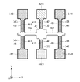
ジャイロ素子2に角速度が加わらない状態において、駆動信号端子452と駆動接地端子462との間に電圧(交番電圧)を印加すると、駆動信号電極451と駆動接地電極461との間に電界が生じ、図6(a)に示すように、各駆動腕341、342、343、344が矢印Aに示す方向に屈曲振動を行う。このとき、第1、第2駆動腕341、342と第3、第4駆動腕343、344とがジャイロ素子2の重心Gを通るYZ平面に関して面対称の振動を行っているため、基部31、第1、第2検出腕321、322および第1、第2連結腕331、332は、ほとんど振動しない。
When a voltage (alternating voltage) is applied between the
このような駆動振動を行っている状態で、ジャイロ素子2にZ軸まわりの角速度ωが加わると、図6(b)に示すような検出振動が励振される。具体的には、駆動腕341、342、343、344および第1、第2連結腕331、332に矢印B方向のコリオリの力が働き、新たな振動が励起される。この矢印B方向の振動は、重心Gに対して周方向の振動である。また同時に、第1、第2検出腕321、322には、矢印Bの振動に呼応して矢印C方向の検出振動が励起される。そして、この振動により第1、第2検出腕321、322に発生した電荷を、第1、第2検出信号電極411、431と第1、第2検出接地電極421、441とから信号として取り出し、この信号に基づいて角速度ωが求められる。
When an angular velocity ω around the Z axis is applied to the
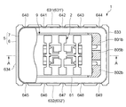
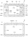
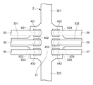
≪パッケージ≫
図1および図2に示すように、パッケージ5は、上面に開口する凹部61を有する箱状のベース(基体)6と、凹部61の開口を塞いでベース6に接合された板状のリッド(蓋体)7と、を有している。そして、凹部61の開口がリッド7によって塞がれることにより形成された内部空間S内に上述したジャイロ素子2が収納されている。内部空間Sの雰囲気は、特に限定されないが、本実施形態では、真空状態(例えば、10Pa以下の減圧状態)となっている。
≪Package≫
As shown in FIG. 1 and FIG. 2, the
−ベース−
ベース6は、その平面視にて、略長方形(矩形)の外形を有しており、長軸方向に延在している一対の外縁631、632と、短軸方向(長軸方向に交差する方向)に延在している一対の外縁633、634と、を有している。ただし、ベース6の平面視形状は、長方形に限定されず、例えば、正方形であってもよいし、五角形以上の多角形であってもよいし、異形であってもよい。
-Base-
The
ここで、本明細書で言う「略長方形」とは、完全な長方形はもちろんの事、実質的に長方形とみなせる形状、具体的には、長方形が有する4つの角部のうちの少なくとも1つの角部が丸み付けされているような形状や、長方形が有する4つの辺のうちの少なくとも1つの辺に湾曲または屈曲した部分が存在しているような形状も含まれることを意味している。 Here, “substantially rectangular” as used in this specification means not only a complete rectangle, but also a shape that can be substantially regarded as a rectangle, specifically, at least one corner of four corners of the rectangle. This means that a shape in which the portion is rounded and a shape in which a curved or bent portion exists on at least one of the four sides of the rectangle are included.
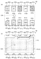
また、ベース6は、酸化アルミニウム質、窒化アルミニウム質、炭化珪素質、ムライト質、ガラス・セラミック質等のセラミックグリーンシートを成形して形成される複数の矩形の基板(シート)を積層した後、焼結して形成されている。積層されるシートの枚数としては特に限定されないが、本実施形態では6枚のシート、具体的には、図2中の下側(リッド7と反対側)から第1基板6A、第2基板6B、第3基板6C、第4基板6D、第5基板6E、第6基板6Fが順に積層されている。
The
また、凹部61は、ベース6の上面に開口する有底の第1凹部611と、第1凹部611の底部に開口し、第1凹部611よりも小さい有底の第2凹部612と、第2凹部612の底部に開口し、第2凹部612よりも小さい有底の第3凹部613と、を有している。このうち、第1凹部611は、第6基板6Fに形成されている貫通孔で構成され、第2凹部612は、第5基板6Eに形成されている貫通孔で構成され、第3凹部613は、第4基板6Dおよび第3基板6Cに連続して形成されている貫通孔で構成されている。また、第5基板6Eには、第2凹部612に繋がる切り欠き651、652が形成されている。
第1凹部611、第2凹部612および第3凹部613は、それぞれ、その平面視にて、略長方形(矩形)の外形をなし、その長軸方向がベース6の長軸方向とほぼ一致している。
The
Each of the
図9(b)に示すように、第1凹部611は、長軸方向に延びている一対の長辺611a、611bと、端軸方向に延びている一対の短辺611c、611dと、を有しており、さらに、各角部が丸みを帯びている。
また、図9(a)に示すように、第2凹部612は、長軸方向に延びている一対の長辺612a、612bと、端軸方向に延びている一対の短辺612c、612dと、を有しており、さらに、各角部が丸みを帯びている。また、ベース6の平面視にて、4つの辺612a〜612dは、それぞれ、第1凹部611よりも内側に位置している。また、辺612cにはベース6の外縁633側へ延びている切り欠き651、652が形成されている。
As shown in FIG. 9B, the
9A, the
また、図8(a)、(b)に示すように、第3凹部613は、長軸方向に延びている一対の長辺613a、613bと、短軸方向に延びている一対の短辺613c、613dと、を有しており、さらに、各角部が丸みを帯びている。また、ベース6の平面視にて、3つの辺612a、612b、612cは、それぞれ、第2凹部612よりも内側に位置し、残りの辺613dは、第2凹部612の短辺612dと重なっている。
このような凹部61の底面(第3凹部613の底面。第2基板6Bの上面)には、IC10が銀(Ag)ペースト等の導電性接着材Kによって固定されている。IC10は、導電性ワイヤー(ボンディングワイヤー)821〜835によって、ベース6に形成された後述する配線群8に電気的に接続されている。
8A and 8B, the
The
また、IC10には、例えば、ジャイロ素子2を駆動振動させるための駆動回路(すなわち駆動信号電極451および駆動接地電極461間に電圧を印加する駆動回路)と、角速度ωが加わったときにジャイロ素子2に生じる検出振動を検出する検出回路(すなわち第1検出信号電極411および第1検出接地電極421間の電荷および第2検出信号電極431および第2検出接地電極441間の電荷を検出する検出回路)と、が組み込まれている。
Further, the
また、IC10は、その平面視にて、略長方形(矩形)の外形をなし、長軸方向がベース6の長軸方向とほぼ一致している。図10に示すように、IC10は、長軸方向に延びている一対の外縁(第1の素子外縁)101、102と、短軸方向(長軸方向に交差する方向)に延在している一対の外縁(第2の素子外縁)103、104と、を有している。ただし、IC10の平面視形状は、長方形に限定されず、例えば、正方形であってもよいし、五角形以上の多角形であってもよいし、異形であってもよい。
The
また、図2に示すように、ベース6の底部には凹部61の内外を連通する貫通孔62が形成されている。この貫通孔62は、内部空間Sを真空引きするための孔であり、貫通孔62を介して内部空間Sの空気を除去した後、Au−Ge系の合金等からなる封止材Mで封止される。これにより、内部空間Sを真空状態に維持することができる。なお、図2では、貫通孔62の内側開口がIC10(導電性接着材K)によって塞がれているように図示されているが、実際には、貫通孔62の内側開口を塞がないように、IC10が固定されている。
Further, as shown in FIG. 2, a through
貫通孔62は、第1基板6Aに形成されている下側貫通孔62Aと、第2基板6Bに形成されている上側貫通孔62Bとで構成されていて、上側貫通孔62Bの径が下側貫通孔62Aの径よりも小さくなっている。そのため、貫通孔62の途中には、第2基板6Bの下面で構成された段差部62Cが形成されている。このような段差部62Cを有することで、封止材Mによる貫通孔62の封止を簡単に行うことができる。具体的には、まず、Au−Ge系の合金等からなり、下側貫通孔62Aよりも小さく上側貫通孔62Bよりも大きい球状の金属ボール(封止材Mとなる材料)を用意し、金属ボールを下側貫通孔62A側から貫通孔62内に導入する。貫通孔62内に導入された金属ボールは、段差部62Cに引っ掛かって留まるため、この金属ボールにレーザー等を照射して溶融することで貫通孔62を封止材Mで封止することができる。
The through
また、ベース6の外縁631、632に対応する側面(長軸方向に延在する側面)631’、632’には、それぞれ、ベース6の上面から下面まで延びる複数の切り欠きが形成されている。具体的には、外縁631に対応する側面631’には、5つの切り欠き640、641、642、643、644がほぼ等間隔に並んで形成されており、外縁632に対応する側面632’には、5つの切り欠き645、646、647、648、649がほぼ等間隔に並んで形成されている。これら各切り欠き640〜649には、配線群8の一部が形成される。
A plurality of cutouts extending from the upper surface to the lower surface of the
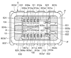
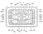
次に、ベース6に配置されている配線群8について図7ないし図10に基づいて詳細に説明する。図7は、(a)が第1基板6Aを上面側から見た透過図、(b)が第2基板6Bの上面図、図8は、(a)が第3基板6Cの上面図、(b)が第4基板6Dの上面図、図8は、(a)が第5基板6Eの上面図、(b)が第6基板6Fの上面図、図10は、ベース6の上面図である。
Next, the
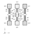
配線群8は、S1配線801と、S2配線802と、接地配線としてのGND配線803と、DS配線804と、DG配線805と、CLK配線806と、DI配線807と、DO配線808と、CS配線809と、VDD1配線810と、TEST1配線811と、DRY配線812と、TEST2配線813と、VDD2配線814と、を有している。なお、これらのうち、本発明の「第2の配線」には、S1配線801、S2配線802、DG配線805が含まれ、本発明の「第1の配線」には、GND配線803、DS配線804、CLK配線806、DI配線807、DO配線808、CS配線809、VDD1配線810、TEST1配線811、DRY配線812、TEST2配線813、VDD2配線814が含まれる。また、配線群8は、上記配線以外の配線を有していてもよいし、上記配線のうちの少なくとも1つが省略されていてもよい。
これら各配線801〜814の構成としては、特に限定されないが、例えば、タングステン(W)、モリブテン(Mo)、マンガン(Mg)などの下地層に、金(Au)などのめっき金属層を積層した金属被膜で構成することができる。めっき金属層は、例えば、電解めっき法によって形成されている。
The
The configuration of each of the
以下、各配線801〜814について順次説明する。
[S1配線]
図8(b)および図9(a)に示すように、S1配線801は、その一端部にS1内部端子801aを有し、その他端部にS1接続端子801bを有している。そして、S1配線801は、S1内部端子801aにおいてIC10と電気的に接続され、S1接続端子801bにおいて第1検出信号端子412と電気的に接続されている。図10に示すように、S1内部端子801aとIC10との電気接続は、導電性ワイヤー821により行われている。一方、S1接続端子801bと第1検出信号端子412との電気接続は、支持基板9を介して行われている。
Hereinafter, the
[S1 wiring]
As shown in FIGS. 8B and 9A, the
S1内部端子801aは、第4基板6Dの上面に形成されており、ベース6の外縁633(IC10の外縁103、第3凹部613の短辺613c)に沿って配置されている。また、S1内部端子801aは、外縁631側に片寄って配置されている。一方、S1接続端子801bは、第5基板6Eの上面に形成され、ベース6の外縁633(第2凹部612の短辺612c)に沿って設けられている。また、S1接続端子801bは、切り欠き651よりも外縁631側に配置されている。
このようなS1配線801は、第4基板6Dと第5基板6Eとに跨って形成されている。第4基板6Dから第5基板6Eへの配線の引き回しは、第5基板6Eに形成されているビア(貫通電極)801cによって行われている。なお、ビア801cは、配線に隠れて見えないが、説明の便宜上、その位置を白丸で示している。
The S1
Such an
[S2配線]
図8(b)および図9(a)に示すように、S2配線802は、その一端部にS2内部端子802aを有し、その他端部にS2接続端子802bを有している。そして、S2配線802は、S2内部端子802aにおいてIC10と電気的に接続され、S2接続端子802bにおいて第2検出信号端子432と電気的に接続されている。図10に示すように、S2内部端子802aとIC10との電気接続は、導電性ワイヤー822により行われている。一方、S2接続端子802bと第1検出信号端子432との電気接続は、支持基板9を介して行われている。
[S2 wiring]
As shown in FIGS. 8B and 9A, the
S2内部端子802aは、第4基板6Dの上面に形成されており、ベース6の外縁633(IC10の外縁103、第3凹部613の短辺613c)に沿って配置されている。また、S2内部端子802aは、外縁632側に片寄って配置されている。一方、S2接続端子802bは、第5基板6Eの上面に形成され、ベース6の外縁633(第2凹部612の短辺612c)に沿って設けられている。また、S2接続端子802bは、切り欠き652よりも外縁632側に配置されている。
The S2
このようなS2配線802は、第4基板6Dと第5基板6Eとに跨って形成されている。第4基板6Dから第5基板6Eへの配線の引き回しは、第5基板6Eに形成されているビア802cによって行われている。なお、ビア802cは、配線に隠れて見えないが、説明の便宜上、その位置を白丸で示している。
以上説明したS1配線801およびS2配線802は、ベース6の平面視にて、ベース6の中心と交わりベース6の長軸に沿った直線L(図8(b)参照)に対して線対称に配置されている。
Such an
The
[DG配線]
図8(b)および図9(a)に示すように、DG配線805は、その一端部にDG内部端子805aを有し、その他端部にDG接続端子805bを有している。そして、DG配線805は、DG内部端子805aにおいてIC10と電気的に接続され、DG接続端子805bにおいて駆動接地端子462と電気的に接続されている。図10に示すように、DG内部端子805aとIC10との電気接続は、導電性ワイヤー823により行われている。一方、DG接続端子805bと駆動接地端子462との電気接続は、支持基板9を介して行われている。
[DG wiring]
As shown in FIGS. 8B and 9A, the
DG内部端子805aは、第4基板6Dの上面に形成され、ベース6の外縁633(IC10の外縁103、第3凹部613の短辺613c)に沿って設けられている。また、DG内部端子805aは、S1内部端子801aとS2内部端子802aの間に配置されている。一方、DG接続端子805bは、第5基板6Eの上面に形成され、ベース6の外縁633(第2凹部612の短辺612c)に沿って設けられている。また、DG接続端子805bは、切り欠き651、652の間(S1、S2接続端子801b、802bの間)に配置されている。
このようなDG配線805は、第4基板6Dと第5基板6Eとに跨って形成されている。第4基板6Dから第5基板6Eへの配線の引き回しは、第5基板6Eに形成されたビア805cにより行われている。なお、ビア805cは、配線に隠れて見えないが、説明の便宜上、その位置を白丸で示している。
The DG
Such a
[CLK配線]
図7および図8に示すように、CLK配線806は、その一端部にCLK内部端子806aを有し、その他端部にCLK外部端子806bを有している。そして、CLK配線806は、CLK内部端子806aにおいてIC10と電気的に接続されている。図10に示すように、CLK内部端子806aとIC10との電気接続は、導電性ワイヤー824により行われている。
[CLK wiring]
As shown in FIGS. 7 and 8, the
CLK内部端子806aは、第4基板6Dの上面に形成され、ベース6の外縁631(IC10の外縁101、第3凹部613の長辺613a)に沿って設けられている。また、CLK内部端子806aは、長辺613aの短辺613d側に配置されている。一方、CLK外部端子806bは、第1基板6Aの下面(ベース6の底面)であって、切り欠き640の近傍に、外縁631に沿って配置されている。
このようなCLK配線806は、第4基板6Dから第1基板6Aに跨って形成されている。第4基板6Dから第1基板6Aへの配線の引き回しは、切り欠き640内に形成されたCLK側面電極806cにより行われており、第4基板6Dの上面に形成されている配線を介してCLK内部端子806aとCLK側面電極806cとが接続されている。
The CLK internal terminal 806a is formed on the upper surface of the
Such a
[DO配線]
図7および図8に示すように、DO配線808は、その一端部にDO内部端子808aを有し、その他端部にDO外部端子808bを有している。そして、DO配線808は、DO内部端子808aにおいてIC10と電気的に接続されている。図10に示すように、DO内部端子808aとIC10との電気接続は、導電性ワイヤー825により行われている。
[DO wiring]
As shown in FIGS. 7 and 8, the DO wiring 808 has a DO internal terminal 808a at one end and a DO external terminal 808b at the other end. The
DO内部端子808aは、第4基板6Dの上面に形成され、ベース6の外縁631(IC10の外縁101、第3凹部613の長辺613a)に沿って配置されている。また、DO内部端子808aは、長辺613aの短辺613d側であって、CLK内部端子806aの右隣に配置されている。一方、DO外部端子808bは、第1基板6Aの下面(ベース6の底面)であって、切り欠き641の近傍に、外縁631に沿って配置されている。
このようなDO配線808は、第4基板6Dから第1基板6Aに跨って形成されている。第4基板6Dから第1基板6Aへの配線の引き回しは、切り欠き641内に形成されたDO側面電極808cによって行われており、第4基板6Dの上面に形成されている配線を介してDO内部端子808aとDO側面電極808cとが接続されている。
The DO internal terminal 808a is formed on the upper surface of the
Such a
[VDD1配線]
図7および図8に示すように、VDD1配線810は、その一端部にVDD1内部端子810aを有し、その他端部にVDD1外部端子810bを有している。そして、VDD1配線810は、VDD1内部端子810aにおいてIC10と電気的に接続されている。図10に示すように、VDD1内部端子810aとIC10との電気接続は、導電性ワイヤー826により行われている。
[VDD1 wiring]
As shown in FIGS. 7 and 8, the
VDD1内部端子810aは、第4基板6Dの上面に形成され、ベース6の外縁631(IC10の外縁101、第3凹部613の長辺613a、)に沿って配置されている。また、VDD1内部端子810aは、長辺613aの短辺613d側であって、DO内部端子808aの右隣に配置されている。一方、VDD1外部端子810bは、第1基板6Aの下面(ベース6の底面)であって、切り欠き642の近傍に、外縁631に沿って配置されている。
The VDD1 internal terminal 810a is formed on the upper surface of the
このようなVDD1配線810は、第4基板6Dから第1基板6Aに跨って形成されている。第4基板6Dから第1基板6Aへの配線の引き回しは、切り欠き642内に形成されたVDD1側面電極810cにより行われており、第4基板6Dの上面に形成されている配線を介してVDD1内部端子810aとVDD1側面電極810cとが接続されている。
Such a
[VDD2配線]
図7および図8に示すように、VDD2配線814は、その一端部にVDD2内部端子814aを有し、その他端部にVDD2外部端子814bを有している。そして、VDD2配線814は、VDD2内部端子814aにおいてIC10と電気的に接続されている。図10に示すように、VDD2内部端子814aとIC10との電気接続は、導電性ワイヤー827により行われている。
[VDD2 wiring]
As shown in FIGS. 7 and 8, the
VDD2内部端子814aは、第4基板6Dの上面に形成され、ベース6の外縁631(IC10の外縁101、第3凹部613の長辺613a)に沿って配置されている。また、VDD2内部端子814aは、長辺613aのほぼ中央部であって、VDD1内部端子810aの右隣に配置されている。一方、VDD2外部端子814bは、第1基板6Aの下面(ベース6の底面)であって、切り欠き644の近傍に、外縁631に沿って配置されている。
The VDD2 internal terminal 814a is formed on the upper surface of the
このようなVDD2配線814は、第4基板6Dから第1基板6Aに跨って形成されている。第4基板6Dから第2基板6Bへの配線の引き回しは、第4基板6Dおよび第3基板6Cに形成されているビア814eにより行われ、第2基板6Bから第1基板6Aへの引き回しは、切り欠き644内に形成されたVDD2側面電極814cにより行われている。なお、ビア814eは、配線に隠れて見えないが、説明の便宜上、その位置を白丸で示している。
Such a
[DRY配線]
図7および図8に示すように、DRY配線812は、その一端部にDRY内部端子812aを有し、その他端部にDRY外部端子812bを有している。そして、DRY配線812は、DRY内部端子812aにおいてIC10と電気的に接続されている。図10に示すように、DRY内部端子812aとIC10との電気接続は、導電性ワイヤー828により行われている。
[DRY wiring]
As shown in FIGS. 7 and 8, the DRY wiring 812 has a DRY internal terminal 812a at one end and a DRY external terminal 812b at the other end. The
DRY内部端子812aは、第4基板6Dの上面に形成され、ベース6の外縁631(IC10の外縁101、第3凹部613の長辺613a)に沿って配置されている。また、DRY内部端子812aは、長辺613aの短辺613c側であって、VDD2内部端子814aの右隣に配置されている。一方、DRY外部端子812bは、第1基板6Aの下面(ベース6の底面)であって、切り欠き643の近傍に、外縁631に沿って配置されている。
このようなDRY配線812は、第4基板6Dから第1基板6Aに跨って形成されている。第4基板6Dから第1基板6Aへの配線の引き回しは、切り欠き644内に形成されたDRY側面電極812cにより行われており、第4基板6Dの上面に形成されている配線を介してDRY内部端子812aとDRY側面電極812cとが接続されている。
The DRY internal terminal 812a is formed on the upper surface of the
Such a
[DS配線]
図7および図8に示すように、DS配線804は、その一端部にDS内部端子804aを有し、その他端部にDS接続端子804bを有している。そして、DS配線804は、DS内部端子804aにおいてIC10と電気的に接続され、DS接続端子804bにおいて駆動信号端子452と電気的に接続されている。図10に示すように、DS内部端子804aとIC10との電気接続は、導電性ワイヤー829によって行われている。一方、DS接続端子804bと駆動信号端子452との電気接続は、支持基板9を介して行われている。
[DS wiring]
As shown in FIGS. 7 and 8, the
DS内部端子804aは、第4基板6Dの上面に形成され、ベース6の外縁632(IC10の外縁102、第3凹部613の長辺613b)に沿って配置されている。また、DS内部端子804aは、長辺613bの短辺613d側に配置されている。一方、DS接続端子804bは、第5基板6Eの上面に形成され、ベース6の外縁634(第2凹部612の短辺612d)に沿って設けられている。また、DS接続端子804bは、短辺612dの中央部に配置されている。
このようなDS配線804は、第4基板6Dと第5基板6Eとに跨って形成されている。第4基板6Dから第5基板6Eへの配線の引き回しは、第5基板6Eに形成されたビア804cによって行われている。なお、ビア804cは、配線に隠れて見えないが、説明の便宜上、その位置を白丸で示している。
The DS
Such a
[DI配線]
図7および図8に示すように、DI配線807は、その一端部にDI内部端子807aを有し、その他端部にDI外部端子807bを有している。そして、DI配線807は、DI内部端子807aにおいてIC10と電気的に接続されている。図10に示すように、DI内部端子807aとIC10との電気接続は、導電性ワイヤー830により行われている。
[DI wiring]
As shown in FIGS. 7 and 8, the
DI内部端子807aは、第4基板6Dの上面に形成され、ベース6の外縁632(IC10の外縁102、第3凹部613の長辺613b)に沿って配置されている。また、DI内部端子807aは、長辺613bの短辺613d側であって、DS内部端子804aの右隣に配置されている。一方、DI外部端子807bは、第1基板6Aの下面(ベース6の底面)であって、切り欠き645の近傍に、外縁632に沿って配置されている。
The DI
このようなDI配線807は、第4基板6Dから第1基板6Aに跨って形成されている。第4基板6Dから第3基板6Cへの配線の引き回しは、第4基板6Dに形成されているビア807eによって行われ、第3基板6Cから第1基板6Aへの引き回しは、切り欠き645内に形成されたDI側面電極807cによって行われている。なお、ビア807eは、配線に隠れて見えないが、説明の便宜上、その位置を白丸で示している。
[CS配線]
図7および図8に示すように、CS配線809は、その一端部にCS内部端子809aを有し、その他端部にCS外部端子809bを有している。そして、CS配線809は、CS内部端子809aにおいてIC10と電気的に接続されている。図10に示すように、CS内部端子809aとIC10との電気接続は、導電性ワイヤー831により行われている。
[CS wiring]
As shown in FIGS. 7 and 8, the
CS内部端子809aは、第4基板6Dの上面に形成され、ベース6の外縁632(ICチップ10の外縁102、第3凹部613の長辺613b)に沿って配置されている。また、CS内部端子809aは、長辺613bの短辺613d側であって、DI内部端子807aの右隣に配置されている。一方、CS外部端子809bは、第1基板6Aの下面(ベース6の底面)であって、切り欠き646の近傍に、外縁632に沿って配置されている。
The CS
このように、CS内部端子809aが第4基板6Dに形成され、CS外部端子809bが第1基板6Aに形成されているため、CS配線809は、第4基板6Dから第1基板6Aに跨って形成されている。第4基板6Dから第1基板6Aへの配線の引き回しは、切り欠き646内に形成されたCS側面電極809cによって行われており、第4基板6Dの上面に形成されている配線を介してCS内部端子809aとCS側面電極809cとが接続されている。
Thus, since the CS
[TEST1配線]
図7および図8に示すように、TEST1配線811は、その一端部にTEST1内部端子811aを有し、その他端部にTEST1外部端子811bを有している。そして、TEST1配線811は、TEST1内部端子811aにおいてIC10と電気的に接続されている。図10に示すように、TEST1内部端子811aとIC10との電気接続は、導電性ワイヤー832により行われている。
[TEST1 wiring]
As shown in FIGS. 7 and 8, the
TEST1内部端子811aは、第4基板6Dの上面に形成され、ベース6の外縁632(IC10の外縁102、第3凹部613の長辺613b)に沿って設けられている。また、TEST1内部端子811aは、長辺613bのほぼ中央部であって、CS内部端子809aの右隣に配置されている。一方、TEST1外部端子811bは、第1基板6Aの下面(ベース6の底面)であって、切り欠き647の近傍に、外縁632に沿って配置されている。
The TEST1 internal terminal 811a is formed on the upper surface of the
このようなTEST1配線811は、第4基板6Dから第1基板6Aに跨って形成されている。第4基板6Dから第1基板6Aへの配線の引き回しは、切り欠き647内に形成されたTEST1側面電極811cによって行われており、第4基板6Dの上面に形成されている配線を介してTEST1内部端子811aとTEST1側面電極811cとが接続されている。
[TEST2配線]
図7および図8に示すように、TEST2配線813は、その一端部にTEST2内部端子813aを有し、その他端部にTEST2外部端子813bを有している。そして、TEST2配線813は、TEST2内部端子813aにおいてIC10と電気的に接続されている。図10に示すように、TEST2内部端子813aとIC10との電気接続は、導電性ワイヤー833により行われている。
[TEST2 wiring]
As shown in FIGS. 7 and 8, the
TEST2内部端子813aは、第4基板6Dの上面に形成され、ベース6の外縁632(IC10の外縁102、第3凹部613の長辺613b)に沿って配置されている。また、TEST2内部端子813aは、長辺613bの短辺613c側であって、TEST1内部端子811aの右隣に配置されている。一方、TEST2外部端子813bは、第1基板6Aの下面(ベース6の底面)であって、切り欠き648の近傍に、外縁632に沿って配置されている。
The TEST2 internal terminal 813a is formed on the upper surface of the
このようなTEST2配線813は、第4基板6Dから第1基板6Aに跨って形成されている。第4基板6Dから第1基板6Aへの配線の引き回しは、切り欠き648内に形成されたTEST2側面電極813cによって行われており、第4基板6Dの上面に形成されている配線を介してTEST2内部端子813aとTEST2側面電極813cとが接続されている。
[GND配線]
図7、図8および図9に示すように、GND配線803は、全ての基板6A〜6Fに跨って形成されている。そして、GND配線803は、各基板6A〜6Fにおいて、他の配線801、802、804〜814の引き回しを阻害しない範囲で、広く拡がって配置されている。具体的には、GND配線803は、第2基板6Bでは大半の領域に、第3、第4基板6C、6Dでは第3凹部613の周囲を囲むように、第5基板6Eでは、第2凹部612の周囲を囲むように「コ」の字状に、第6基板6Fでは第1凹部611の周囲を囲む環状に、それぞれ、設けられている。
なお、第6基板6Fに配置されているGND配線803は、リッド7との接合に用いられるメタライズ層803’としても機能する。
[GND wiring]
As shown in FIGS. 7, 8, and 9, the
The
GND配線803は、GND内部端子803a’、803a”と、GND接続端子803b’、803b”と、GND外部端子803cと、を有している。そして、GND配線803は、GND内部端子803a’、803a”の少なくとも一方(本実施形態ではGND内部端子803a”)において、IC10と電気的に接続され、GND接続端子803b’、803b”において第1、第2検出接地端子422、442と電気的に接続されている。図10に示すように、GND内部端子803a”とIC10との電気接続は、導電性ワイヤー835によって行われている。一方、GND接続端子803b’、803b”と第1、第2検出接地端子422、442との電気接続は、支持基板9を介して行われている。
The
GND内部端子803a’は、第4基板6Dの上面に形成され、DRY内部端子812aとS1内部端子801aとの間に配置されている。一方、GND内部端子803a”は、第4基板6Dの上面に形成され、TEST2内部端子813aとS2内部端子802aとの間に配置されている。GND内部端子803a’、803a”をこのように配置とすることで、GND内部端子803a’、803a”により、S1、S2内部端子801a、802aと、内部端子803a、804a、806a〜814aとが隔てられた状態となる。
The GND internal terminal 803a 'is formed on the upper surface of the
また、GND接続端子803b’、803b”は、それぞれ、第5基板6Eの上面に形成され、ベース6の外縁634(第2凹部612の短辺612d)に沿って設けられている。また、GND接続端子803b’は、外縁631側に配置され、GND接続端子803b”は、外縁632側に配置されている。すなわち、GND接続端子803b’、803b”は、DS接続端子804bを間に挟むように配置されている。これらGND接続端子803b’、803b”は、第5基板6Eの上面に形成され、第2凹部612の3辺612a、612c、612bの外側をまわり込むようにして配置されたGND配線803により電気的に接続されている。
In addition, the
また、GND外部端子803cは、第1基板6Aの下面(ベース6の底面)であって、切り欠き649の近傍に、外縁632に沿って配置されている。
また、各基板6A〜6F上のGND配線803は、切り欠き649に形成されているGND側面電極803dや、第3基板6C〜第6基板6Fに形成されているビア803eを介して電気的に接続されている。具体的には、第6基板6Fから第5基板6Eへの配線の引き回しは、第6基板6Fに形成された複数のビア803eにより行われ、第5基板6Eから第4基板6Dへの配線の引き回しは、第5基板6Eに形成されたビア803eにより行われ、第4基板6Dから第3基板6Cへの配線の引き回しは、第4基板6Dに形成されたビア803eにより行われ、第3基板6Cから第2基板6Bへの配線引き回しおよび第2基板6Bから第1基板6Aへの配線の引き回しは、それぞれ、切り欠き659に形成されたGND側面電極803dにより行われている。なお、ビア803eは、配線に隠れて見えないが、説明の便宜上、その位置を白丸で示している。
The GND
The
−リッド7−
図1および図2に示すように、リッド7は、板状であり、角部が丸み付けされた略長方形状をなしている。このようなリッド7は、例えば、その下面に配置されている図示しない金属ろう材を介してベース6の上面に設けられているメタライズ層803’(GND配線803)に接合されている。
-Lid 7-
As shown in FIGS. 1 and 2, the
リッド7の構成材料としては、特に限定されないが、ベース6の構成材料と線膨張係数が近似する部材であると良い。例えば、ベース6の構成材料を前述のようなセラミックスとした場合には、コバール等の合金とするのが好ましい。また、リッド7の構成材料をコバール等の合金とすることで、リッド7をGND配線803に電気的に接続することができる。そのため、リッド7をパッケージ5の外部からのノイズを遮断するシールド部として機能させることができる。
The constituent material of the
≪支持基板≫
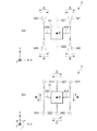
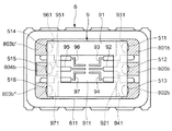
支持基板9は、従来から知られるTAB(Tape Automated Bonding)実装用の基板である。
図1および図11に示すように、支持基板9は、枠状の基部91と、基部91に設けられた6本のボンディングリード(配線)92、93、94、95、96、97と、を有している。
基部91は、例えば、ポリイミド等の可撓性を有する樹脂で構成されている。また、基部91は、略長方形の外形形状を有しており、その長軸がパッケージ5の長軸と一致するように第1凹部611内に配置されている。
≪Support substrate≫
The
As shown in FIGS. 1 and 11, the
The
6本のボンディングリード92〜97は、それぞれ、図示しない接着材によって基部91の下面に固定されている。また、ボンディングリード92、93、94は、基部91の図中左側(長軸方向の一方側)の部分に配置されており、その先端部が基部91の開口部911内まで延びている。一方、ボンディングリード95、96、97は、基部91の図中右側(長軸方向の他方側)の部分に配置されており、その先端部が基部91の開口部911内まで延びている。
そして、ボンディングリード92、93、94の先端部とボンディングリード95、96、97の先端部とが、開口部911の中央で対向している。
Each of the six bonding leads 92 to 97 is fixed to the lower surface of the base 91 with an adhesive (not shown). The bonding leads 92, 93, 94 are disposed on the left side (one side in the long axis direction) of the base 91 in the drawing, and the tip ends thereof extend into the
The leading ends of the bonding leads 92, 93, and 94 are opposed to the leading ends of the bonding leads 95, 96, and 97 at the center of the
また、ボンディングリード92〜97は、それぞれ、途中で傾斜しており、先端部が基部91よりも上方に位置している。また、ボンディングリード92〜97は、途中で幅が狭くなっており、先端部が基端部よりも細くなっている。また、ボンディングリード92〜96の先端部は、ジャイロ素子2が有する第1検出信号端子412、第1検出接地端子422、第2検出信号端子432、第2検出接地端子442、駆動信号端子452、駆動接地端子462に対応して(重なるように)配置されている。
Each of the bonding leads 92 to 97 is inclined in the middle, and the tip portion is located above the
また、ボンディングリード92、95の基端部は、接続端子921、951となっており、ボンディングリード92、95は、接続端子921、951から真っ直ぐに延びている。一方、ボンディングリード93、94、96、97の基端部は、接続端子931、941、961、971となっており、ボンディングリード93、94、96、97は、接続端子931、941、961、971からボンディングリード92、95側に直角に屈曲しながら延びている。そして、これら接続端子921〜971は、ベース6に設けられているS1接続端子801b、S2接続端子802b、GND接続端子803b’、803b”、DS接続端子804bおよびDG接続端子805bに重なるように配置されている。
The base ends of the bonding leads 92 and 95 are
以上のような構成の支持基板9は、導電性接着材を介してベース6およびジャイロ素子2と接合されている。具体的には、図12に示すように、支持基板9とベース6は、6つの導電性接着材511〜516を介して接合されている。導電性接着材511は、接続端子931とS1接続端子801bとに接触して設けられ、これらを電気的に接続している。また、導電性接着材512は、接続端子921とDG接続端子805bとに接触して設けられ、これらを電気的に接続している。また、導電性接着材513は、接続端子941とS2接続端子802bとに接触して設けられ、これらを電気的に接続している。また、導電性接着材514は、接続端子961とGND接続端子803b’とに接触して設けられ、これらを電気的に接続している。また、導電性接着材515は、接続端子951とDS接続端子804bとに接触して設けられ、これらを電気的に接続している。また、導電性接着材516は、接続端子971とGND接続端子803b”とに接触して設けれ、これらを電気的に接続している。これにより、支持基板9がベース6に固定されるともに、電気的に接続される。
The
また、図13に示すように、支持基板9とジャイロ素子2は、6つの導電性接着材521〜526を介して接合されている。導電性接着材521は、ボンディングリード93の先端部と第1検出信号端子412とに接触して設けられ、これらを電気的に接続している。また、導電性接着材522は、ボンディングリード92の先端部と駆動接地端子462とに接触して設けられ、これらを電気的に接続している。また、導電性接着材523は、ボンディングリード94の先端部と第2検出信号端子432とに接触して設けられ、これらを電気的に接続している。また、導電性接着材524は、ボンディングリード96の先端部と第1検出接地端子422とに接触して設けられ、これらを電気的に接続している。また、導電性接着材525は、ボンディングリード95の先端部と駆動信号端子452とに接触して設けられ、これらを電気的に接続している。また、導電性接着材526は、ボンディングリード97の先端部と第2検出接地端子442とに接触して設けられ、これらを電気的に接続している。これにより、ジャイロ素子2が支持基板9に固定されるともに、電気的に接続される。
As shown in FIG. 13, the
導電性接着材511〜516、521〜526としては、導電性および接着性を有していれば、特に限定されず、例えば、シリコーン系、エポキシ系、アクリル系、ポリイミド系、ビスマレイミド系等の接着材に、銀粒子等の導電性フィラーを分散させたものを用いることができる。なお、導電性接着材に替えて、金バンプ、半田等を用いて支持基板9とベース6、支持基板9とジャイロ素子2を接合してもよい。
以上、物理量センサー1の構成について詳細に説明した。このような構成の物理量センサー1では、主に、次のような効果を発揮することができる。
The
The configuration of the physical quantity sensor 1 has been described in detail above. The physical quantity sensor 1 having such a configuration can mainly exhibit the following effects.
(第1の効果)
第1に、物理量センサー1では、複数の第1の配線(配線803、804、806、807、808、809、810、811、812、813、814)の内部端子(内部端子803a、804a、806a、807a、808a、809a、810a、811a、812a、813a、814a)は、ベース6の長軸方向に沿う第1の軸J1に沿って並んで配置されており、複数の第2の配線(配線801、802、805)の内部端子(内部端子801a、802a、805a)は、第1の軸J1に交差し、ベース6の短軸方向に沿う第2の軸J2に沿って並んで配置されている。また、複数の第1の配線には、デジタル信号配線(CLK配線806、DI配線807、DO配線808およびCS配線809)が含まれており、これらの内部端子806a、807a、808a、809aが、複数の第1の配線の内部端子における第1の軸J1方向の中央線Jcに対して、第2の軸J2と反対側に配置されている。ここで、デジタル信号配線で伝送されるデジタル信号は、特に前述のノイズ源になり易い。そのため、物理量センサー1では、上記配置とすることで、S1、S2配線801、802とデジタル信号配線とを大きく離間させ、これにより、デジタル信号配線からS1、S2配線801、802へのノイズ干渉が効果的に低減されている。したがって、物理量センサー1によれば、S1、S2配線801、802へのノイズ干渉が低減され、高精度に角速度ωを検出することができる。
(First effect)
First, in the physical quantity sensor 1, a plurality of first wirings (
(第2の効果)
第2に、前述したように、物理量センサー1では、ベース6の外縁(第1の外縁)631、632に対応する側面631’、632’に、第1の配線が有する側面電極(803d、806c、807c、807c、808c、809c、810c、811c、812c、813c、814c)が配置されている。これにより、S1、S2配線801、802と、各側面電極とを離間させることができる。したがって、第1の配線からS1、S2配線801、802へのノイズ干渉が低減され、高精度に角速度ωを検出することができる。特に、本実施形態では、デジタル信号配線の側面電極806c、807c、808c、809cを、S1、S2内部端子801a、802aと反対側に配置したことで、これら側面電極806c、807c、808c、809cと、S1、S2配線801、802とをより大きく離間させている。したがって、上記効果がより顕著となり、物理量センサー1は、より高精度に角速度ωを検出することができる。
(Second effect)
Secondly, as described above, in the physical quantity sensor 1, the side electrodes (803d, 806c) of the first wiring are provided on the side surfaces 631 ′, 632 ′ corresponding to the outer edges (first outer edges) 631, 632 of the
(第3の効果)
第3に、前述したように、物理量センサー1では、ベースの底面には、外縁(第1の外縁)631、632に沿って、CLK外部端子806bと、DO外部端子808bと、VDD1外部端子810bと、VDD2外部端子814bと、DRY外部端子812bと、DI外部端子807bと、CS外部端子809bと、TEST1外部端子811bと、TEST2外部端子813bと、が配置されている。このような外部端子の配置とすることで、パッケージサイズを維持したまま、S1、S2配線801、802と、各外部端子806b〜814bとをなるべく大きく離間させることができる。したがって、他の配線(特に側面電極)からS1、S2配線801、802へのノイズ干渉が低減され、高精度に角速度ωを検出することができる。
(Third effect)
Third, as described above, in the physical quantity sensor 1, the CLK
特に、本実施形態では、デジタル信号を伝送するCLK配線806、DI配線807、DO配線808、CS配線809の外部端子806b、807b、808b、809bを外縁631、632の、S1、S2内部端子801a、802aと反対側に配置したことで、これら外部端子806b、807b、808b、809bと、S1、S2配線801、802とをより大きく離間させている。したがって、上記効果がより顕著となり、物理量センサー1は、より高精度に角速度ωを検出することができる。
In particular, in this embodiment, the
(第4の効果)
第4に、前述したように、物理量センサー1では、S1配線801と、CLK配線806、DO配線808、VDD1配線810、VDD2配線814およびDRY配線812との間に、GND配線803(GND内部端子803a’)が配置されており、同様に、S2配線802と、DS配線804、DI配線807、CS配線809、TEST1配線811およびTEST2配線813との間にGND配線803(GND内部端子803a”)が配置されている。そのため、GND配線803がノイズを遮断するシールド層として機能し、CLK配線806、DO配線808、VDD1配線810、VDD2配線814およびDRY配線812からのノイズのS1、S2配線801、802への混入、および、DS配線804、DI配線807、CS配線809、TEST1配線811およびTEST2配線813からのノイズのS1、S2配線801、802への混入を、それぞれ、低減している。したがって、他の配線からS1、S2配線801、802へのノイズ干渉が低減され、高精度に角速度ωを検出することができる。
特に、本実施形態のように、CLK配線806、DI配線807、DO配線808、CS配線809と、S1、S2配線801、802との間に、GND配線803を配置することによって、上述した理由と同様の理由で、上記効果がより顕著となり、より高精度に角速度ωを検出することができる。
(Fourth effect)
Fourth, as described above, in the physical quantity sensor 1, the GND wiring 803 (GND internal terminal) is connected between the
In particular, by arranging the
なお、本実施形態では、S1配線801と配線806、808、810、814、812との間、および、S2配線802と配線804、807、809、811、813との間に、それぞれ、GND配線803が配置されているが、これに替えて、電位が固定されている固定電位配線を配置しても同様の効果を発揮することができる。固定電位配線としては、例えば、電源配線を用いることができる。
In the present embodiment, the GND wiring is between the
(第5の効果)
第5に、デジタル信号配線としてのCLK内部端子806a、DO内部端子808a、DI内部端子807a、CS内部端子809aに接続される導電性ワイヤー824、825、830、831の延在方向と、検出信号配線の内部端子としてのS1、S2内部端子801a、802aに接続される導電性ワイヤー821、822の延在方向とが直交している。詳述すれば、導電性ワイヤー824、825、830、831にデジタル信号が流れることにより、当該導電性ワイヤーの軸を中心として、同心円状に磁界が発生する。
(Fifth effect)
Fifth, the extending direction of the
ここで、導電性ワイヤー824、825、830、831と平面視において平行な他の導電性ワイヤー(以下、平行導電性ワイヤーと称する)について説明する。平行導電性ワイヤーは、平面視においては略直線であるが、断面視においては完全な直線ではなく閉ループの一部を形成している。平行導電性ワイヤーの周囲に発生した前述の磁界のベクトルは、閉ループの面に直交する成分を有するため、平行導電性ワイヤーに誘導電流が流れる。結果として、平行導電性ワイヤーに電気的なノイズ信号が重畳される。
Here, the
次に、導電性ワイヤー824、825、830、831と平面視において直交する導電性ワイヤー821、822について説明する。導電性ワイヤー821、822は、平面視においては略直線であるが、断面視においては完全な直線ではなく閉ループの一部を形成している。しかしながら、導電性ワイヤー821、822の周囲に発生した前述の磁界のベクトルは、閉ループの面と略平行であるため、導電性ワイヤー821、822に流れる誘導電流を抑制できる。結果として、導電性ワイヤー824、825、830、831にデジタル信号が流れることにより、導電性ワイヤー821、822に発生するノイズ信号を抑制できる。
なお、導電性ワイヤー824、825、830、831の延在方向と、導電性ワイヤー821、822の延在方向とが、直交している例で説明したが、交差している場合でも、導電性ワイヤー821、822へ電気的なノイズ信号が重畳されることを抑制できる。
Next, the
In addition, although the example in which the extending direction of the
また、前述したように、物理量センサー1では、CLK内部端子806a、DO内部端子808a、VDD1内部端子810、VDD2内部端子814a、DRY内部端子812a、DS内部端子804a、DI内部端子807a、CS内部端子809a、TEST1内部端子811aおよびTEST2内部端子813aと、IC10とが、導電性ワイヤー824〜835で接続され、S1、S2内部端子801a、802aと、IC10とが、導電性ワイヤー821、822で接続されている。そして、物理量センサー1では、ベース6の平面視にて、導電性ワイヤー824〜835の延在方向と、導電性ワイヤー821、822の延在方向とが交差している。具体的には、導電性ワイヤー824〜835は、ベース6の短軸方向に延在しているのに対して、導電性ワイヤー821、822は、ベース6の長軸方向に延在している。すなわち、導電性ワイヤー824〜835の延在方向と、導電性ワイヤー821、822の延在方向とが直交している。このような配置とすることで、パッケージサイズを維持したまま、導電性ワイヤー821、822と、導電性ワイヤー824〜835とをなるべく大きく離間させることができる。したがって、他の配線からS1、S2配線801、802へのノイズ干渉が低減され、高精度に角速度ωを検出することができる。
As described above, in the physical quantity sensor 1, the CLK internal terminal 806a, the DO internal terminal 808a, the VDD1
(第6の効果)
第6に、前述したように、物理量センサー1では、各内部端子801a〜814aが形成されている第4基板6Dを挟み込むように第3基板6Cと第5基板6Eとが配置されており、これら第3、第5基板6C、6Eには、それぞれ、GND配線803が設けられている。これにより、第4基板6D上に配置されている各配線801、802、804〜814が、GND配線803によって挟み込まれた構成となっている。前述したように、GND配線803は、S1、S2配線801、802へのノイズの混入を低減するシールド層として機能する。そのため、このような構成とすることによって、他の配線からS1、S2配線801、802へのノイズ干渉が低減され、高精度に角速度ωを検出することができる。
(Sixth effect)
Sixth, as described above, in the physical quantity sensor 1, the
(第7の効果)
第7に、物理量センサー1では、ボンディングリード93が、S1配線801(S1内部端子801a)と重なるように配置されている。このように、S1配線801と電気的に接続されているボンディングリード93をS1配線801に近接して配置することにより、相対的に、S1配線801と電気的に接続されていない他のボンディングリード92、94をS1配線801から離間させることができる。そのため、ボンディングリード92、94からS1配線801へのノイズ干渉を低減することができる。
(Seventh effect)
Seventh, in the physical quantity sensor 1, the
同様に、ボンディングリード94が、S2配線802(S2内部端子802a)と重なるように配置されている。このように、S2配線802と電気的に接続されているボンディングリード94をS2配線802に近接して配置することにより、相対的に、S2配線802と電気的に接続されていない他のボンディングリード92、93をS2配線802から離間させることができる。そのため、ボンディングリード92、92からS2配線802へのノイズ干渉を低減することができる。
以上、物理量センサー1が発揮することのできる効果について説明した。
Similarly, the
In the above, the effect which the physical quantity sensor 1 can demonstrate was demonstrated.
上記効果を裏付けるためのシミュレーション結果を書きの表1に示す。表1中の「本実施形態」は、本実施形態の物理量センサーに対応し、S1内部端子801aおよびS2内部端子802aを第4基板6Dの短辺613cに沿って配置したときの各配線間の容量結合の大きさを示している。一方、表1中の「従来」は、従来の物理量センサーに対応し、例えば、S1内部端子801aを第4基板6Dの外縁631(長辺613a)に沿って配置し、S2内部端子802aを外縁632(長辺613b)に沿って配置したときの各配線間の容量結合の大きさを示している。
Table 1 shows the simulation results to support the above effect. “This embodiment” in Table 1 corresponds to the physical quantity sensor of this embodiment, and between the wirings when the S1 internal terminal 801a and the S2
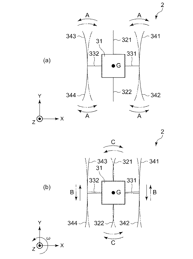
表1から分かるように、本実施形態の物理量センサーの方がS1、S2配線801、802と他の配線との間の容量結合が小さい。特に、CS配線、VDD1配線、VDD2配線との間の容量結合が顕著に小さくなっている。したがって、物理量センサー1によれば、他の配線からS1、S2配線801、802へのノイズ干渉が低減され、角速度ωをより正確に検出することができる。 As can be seen from Table 1, the physical quantity sensor of this embodiment has smaller capacitive coupling between the S1 and S2 wirings 801 and 802 and the other wirings. In particular, the capacitive coupling between the CS wiring, the VDD1 wiring, and the VDD2 wiring is remarkably reduced. Therefore, according to the physical quantity sensor 1, noise interference from other wirings to the S1 and S2 wirings 801 and 802 is reduced, and the angular velocity ω can be detected more accurately.
<第2実施形態>
図14は、本発明の第2実施形態に係る物理量センサーの平面図(上面図)である。
以下、第2実施形態の物理量センサーについて前述した実施形態との相違点を中心に説明し、同様の事項については、その説明を省略する。
第2実施形態の物理量センサーは、ジャイロ素子の構成が異なることと、それに伴って支持基板が省略されていること以外は、前述した第1実施形態の物理量センサーと同様である。なお、図14では、前述した実施形態と同様の構成には同一符号を付してある。
図14に示すように、本実施形態の物理量センサー1は、前述した第1実施形態と比べて支持基板9が省略された構成となっている。
Second Embodiment
FIG. 14 is a plan view (top view) of a physical quantity sensor according to the second embodiment of the present invention.
Hereinafter, the physical quantity sensor of the second embodiment will be described with a focus on differences from the above-described embodiment, and description of similar matters will be omitted.
The physical quantity sensor of the second embodiment is the same as the physical quantity sensor of the first embodiment described above except that the configuration of the gyro element is different and the support substrate is omitted accordingly. In FIG. 14, the same reference numerals are given to the same components as those in the above-described embodiment.
As shown in FIG. 14, the physical quantity sensor 1 of the present embodiment has a configuration in which the
≪ジャイロ素子≫
本実施形態のジャイロ素子2は、前述した第1実施形態のジャイロ素子2と比べて、第1、第2支持部351、352と、第1、第2、第3、第4梁361、362、363、364と、を追加した構成となっている。
第1、第2支持部351、352は、基部31を介してY軸方向に対向配置されている。また、第1、第2支持部351、352は、それぞれ、X軸方向に延在して配置されている。そして、基部31は、第1、第3梁361、363によって第1支持部351に支持されており、第2、第4梁362、364によって第2支持部352に支持されている。
≪Gyro element≫
The
The first and
第1梁361は、第1検出腕321と第1駆動腕341との間を通って基部31と第1支持部351とを連結している。また、第2梁362は、第2検出腕322と第2駆動腕342との間を通って基部31と第2支持部352とを連結している。また、第3梁363は、第1検出腕321と第3駆動腕343との間を通って基部31と第1支持部351とを連結している。また、第4梁364は、第2検出腕322と第4駆動腕344との間を通って基部31と第2支持部352とを連結している。これら梁361、362、363、364は、重心Gに関して点対称に配置されている。また、各梁361、362、363、364は、X軸方向に沿って往復しながらY軸方向に沿って延びる蛇行部(S字形状部)を有しており、X軸方向およびY軸方向に弾性を有している。これにより、各梁361、362、363、364で衝撃を吸収でき、衝撃に起因する検出ノイズを低減または抑制することができる。
The
このようなジャイロ素子2では、第1支持部351の中央部に駆動接地端子462が配置されており、−X軸方向の端部に第1検出信号端子412が配置されており、+X軸方向の端部に第2検出信号端子432が配置されている。また、第2支持部352の中央部に駆動信号端子452が配置されており、−X軸方向の端部に第1検出接地端子422が配置されており、+X軸方向の端部に第2検出接地端子442が配置されている。
In such a
本実施形態では、このようなジャイロ素子2が、6つの導電性接着材531〜536によってベース6に接合されている。導電性接着材531は、第1検出信号端子412とS1接続端子801bとに接触して設けられ、これらを電気的に接続している。また、導電性接着材532は、駆動接地端子462とDG接続端子805bとに接触して設けられ、これらを電気的に接続している。また、導電性接着材533は、第2検出信号端子432とS2接続端子802bとに接触して設けられ、これらを電気的に接続している。また、導電性接着材534は、第1検出接地端子422とGND接続端子803b’とに接触して設けられ、これらを電気的に接続している。また、導電性接着材535は、駆動信号端子452とDS接続端子804bとに接触して設けられ、これらを電気的に接続している。また、導電性接着材556は、第2検出接地端子442とGND接続端子803b”とに接触して設けれ、これらを電気的に接続している。これにより、ジャイロ素子2がベース6に固定されるともに、電気的に接続される。
In the present embodiment, such a
2.電子機器
次いで、物理量センサー1を適用した電子機器について、図15〜図17に基づき、詳細に説明する。
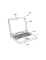
図15は、本発明の物理量センサーを備える電子機器を適用したモバイル型(またはノート型)のパーソナルコンピューターの構成を示す斜視図である。この図において、パーソナルコンピューター1100は、キーボード1102を備えた本体部1104と、表示部1108を備えた表示ユニット1106とにより構成され、表示ユニット1106は、本体部1104に対しヒンジ構造部を介して回動可能に支持されている。このようなパーソナルコンピューター1100には、角速度検知手段として機能する物理量センサー1が内蔵されている。
2. Electronic Device Next, an electronic device to which the physical quantity sensor 1 is applied will be described in detail with reference to FIGS.
FIG. 15 is a perspective view illustrating a configuration of a mobile (or notebook) personal computer to which an electronic device including the physical quantity sensor of the present invention is applied. In this figure, a
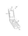
図16は、本発明の物理量センサーを備える電子機器を適用した携帯電話機(PHSも含む)の構成を示す斜視図である。この図において、携帯電話機1200は、複数の操作ボタン1202、受話口1204および送話口1206を備え、操作ボタン1202と受話口1204との間には、表示部1208が配置されている。このような携帯電話機1200には、角速度検知手段として機能する物理量センサー1が内蔵されている。
FIG. 16 is a perspective view illustrating a configuration of a mobile phone (including PHS) to which an electronic device including the physical quantity sensor of the present invention is applied. In this figure, a
図17は、本発明の物理量センサーを備える電子機器を適用したディジタルスチルカメラの構成を示す斜視図である。なお、この図には、外部機器との接続についても簡易的に示されている。ここで、通常のカメラは、被写体の光像により銀塩写真フィルムを感光するのに対し、ディジタルスチルカメラ1300は、被写体の光像をCCD(Charge Coupled Device)などの撮像素子により光電変換して撮像信号(画像信号)を生成する。
FIG. 17 is a perspective view illustrating a configuration of a digital still camera to which an electronic device including the physical quantity sensor of the present invention is applied. In this figure, connection with an external device is also simply shown. Here, an ordinary camera sensitizes a silver halide photographic film with a light image of a subject, whereas a
ディジタルスチルカメラ1300におけるケース(ボディー)1302の背面には、表示部が設けられ、CCDによる撮像信号に基づいて表示を行う構成になっており、表示部1310は、被写体を電子画像として表示するファインダーとして機能する。
また、ケース1302の正面側(図中裏面側)には、光学レンズ(撮像光学系)やCCDなどを含む受光ユニット1304が設けられている。
撮影者が表示部に表示された被写体像を確認し、シャッターボタン1306を押下すると、その時点におけるCCDの撮像信号が、メモリー1308に転送・格納される。
A display unit is provided on the back of a case (body) 1302 in the
A
When the photographer confirms the subject image displayed on the display unit and presses the
また、このディジタルスチルカメラ1300においては、ケース1302の側面に、ビデオ信号出力端子1312と、データ通信用の入出力端子1314とが設けられている。そして、図示されるように、ビデオ信号出力端子1312にはテレビモニター1430が、デ−タ通信用の入出力端子1314にはパーソナルコンピューター1440が、それぞれ必要に応じて接続される。さらに、所定の操作により、メモリー1308に格納された撮像信号が、テレビモニター1430や、パーソナルコンピューター1440に出力される構成になっている。
このようなディジタルスチルカメラ1300には、角速度検知手段として機能する物理量センサー1が内蔵されている。
In the
Such a
なお、本発明の物理量センサーを備える電子機器は、図15のパーソナルコンピューター(モバイル型パーソナルコンピューター)、図16の携帯電話機、図17のディジタルスチルカメラの他にも、例えば、インクジェット式吐出装置(例えばインクジェットプリンター)、ラップトップ型パーソナルコンピューター、テレビ、ビデオカメラ、ビデオテープレコーダー、カーナビゲーション装置、ページャ、電子手帳(通信機能付も含む)、電子辞書、電卓、電子ゲーム機器、ワードプロセッサー、ワークステーション、テレビ電話、防犯用テレビモニター、電子双眼鏡、POS端末、医療機器(例えば電子体温計、血圧計、血糖計、心電図計測装置、超音波診断装置、電子内視鏡)、魚群探知機、各種測定機器、計器類(例えば、車両、航空機、船舶の計器類)、フライトシュミレーター等に適用することができる。 In addition to the personal computer (mobile personal computer) shown in FIG. 15, the mobile phone shown in FIG. 16, and the digital still camera shown in FIG. Inkjet printers), laptop personal computers, televisions, video cameras, video tape recorders, car navigation devices, pagers, electronic notebooks (including those with communication functions), electronic dictionaries, calculators, electronic game devices, word processors, workstations, televisions Telephone, crime prevention TV monitor, electronic binoculars, POS terminal, medical equipment (for example, electronic thermometer, blood pressure monitor, blood glucose meter, electrocardiogram measuring device, ultrasonic diagnostic device, electronic endoscope), fish detector, various measuring devices, instruments Type (e.g., vehicle, Sky machine, gauges of a ship), can be applied to a flight simulator or the like.
3.移動体
次いで、図1に示す物理量センサーを適用した移動体について、図18に基づき、詳細に説明する。
図18は、本発明の物理量センサーを備える移動体を適用した自動車の構成を示す斜視図である。自動車1500には、角速度検知手段として機能する物理量センサー1が内蔵されており、物理量センサー1によって車体1501の姿勢を検出することができる。物理量センサー1からの信号は、車体姿勢制御装置1502に供給され、車体姿勢制御装置1502は、その信号に基づいて車体1501の姿勢を検出し、検出結果に応じてサスペンションの硬軟を制御したり、個々の車輪1503のブレーキを制御したりすることができる。その他、このような姿勢制御は、二足歩行ロボットやラジコンヘリコプターで利用することができる。以上のように、各種移動体の姿勢制御の実現にあたって、物理量センサー1が組み込まれる。
3. Next, a moving body to which the physical quantity sensor shown in FIG. 1 is applied will be described in detail with reference to FIG.
FIG. 18 is a perspective view showing a configuration of an automobile to which a moving body including a physical quantity sensor of the present invention is applied. The
以上、本発明のパッケージ、電子部品搭載パッケージ、物理量センサー、電子機器および移動体を図示の実施形態に基づいて説明したが、本発明はこれに限定されるものではなく、各部の構成は、同様の機能を有する任意の構成のものに置換することができる。また、本発明に、他の任意の構成物が付加されていてもよい。また、本発明は、前記各実施形態のうちの、任意の2以上の構成(特徴)を組み合わせたものであってもよい。 As described above, the package, the electronic component mounting package, the physical quantity sensor, the electronic device, and the moving body according to the present invention have been described based on the illustrated embodiment. It can be replaced with any configuration having the above function. In addition, any other component may be added to the present invention. Further, the present invention may be a combination of any two or more configurations (features) of the above embodiments.
1……物理量センサー 2……ジャイロ素子 3……振動片 31……基部 321……第1検出腕 3211……ハンマーヘッド 322……第2検出腕 3221……ハンマーヘッド 331……第1連結腕 332……第2連結腕 341……第1駆動腕 3411……ハンマーヘッド 342……第2駆動腕 3421……ハンマーヘッド 343……第3駆動腕 3431……ハンマーヘッド 344……第4駆動腕 3441……ハンマーヘッド 351……第1支持部 352……第2支持部 361……第1梁 362……第2梁 363……第3梁 364……第4梁 411……第1検出信号電極 412……第1検出信号端子 421……第1検出接地電極 422……第1検出接地端子 431……第2検出信号電極 432……第2検出信号端子 441……第2検出接地電極 442……第2検出接地端子 451……駆動信号電極 452……駆動信号端子 461……駆動接地電極 462……駆動接地端子 5……パッケージ 511〜516、521〜526、531〜536……導電性接着材 6……ベース 6A……第1基板 6B……第2基板 6C……第3基板 6D……第4基板 6E……第5基板 6F……第6基板 61……凹部 611……第1凹部 611a、611b……長辺 611c、611d……短辺 612……第2凹部 612a、612b……長辺 612c、612d……短辺 613……第3凹部 613a、613b……長辺 613c、613d……短辺 62……貫通孔 62A……下側貫通孔 62B……上側貫通孔 62C……段差部 631、632……側面 640〜649……切り欠き 7……リッド 8……配線群 801……S1配線 801a……S1内部端子 801b……S1接続端子 801c……ビア 802……S2配線 802a……S2内部端子 802b……S2接続端子 802c……ビア 803……GND配線 803’……メタライズ層 803a’、803a”……GND内部端子 803b’、803b”……GND接続端子 803c……GND外部端子 803d……GND側面電極 803e……ビア 804……DS配線 804a……DS内部端子 804b……DS接続端子 804c……ビア 805……DG配線 805a……DG内部端子 805b……DG接続端子 805c……ビア 806……CLK配線 806a……CLK内部端子 806b……CLK外部端子 806c……CLK側面電極 807……DI配線 807a……DI内部端子 807b……DI外部端子 807c……DI側面電極 808……DO配線 808a……DO内部端子 808b……DO外部端子 808c……DO側面電極 809……CS配線 809a……CS内部端子 809b……CS外部端子 809c……CS側面電極 810……VDD1配線 810a……VDD1内部端子 810b……VDD1外部端子 810c……VDD1側面電極 811……TEST1配線 811a……TEST1内部端子 811b……TEST1外部端子 811c……TEST1側面電極 812……DRY配線 812a……DRY内部端子 812b……DRY外部端子 812c……DRY側面電極 813……TEST2配線 813a……TEST2内部端子 813b……TEST2外部端子 813c……TEST2側面電極 814……VDD2配線 814a……VDD2内部端子 814b……VDD2外部端子 814c……VDD2側面電極 821〜835……導電性ワイヤー 9……支持基板 91……基部 911……開口部 92〜97……ボンディングリード 921〜971……接続端子 10……IC 101、102、103、104……外縁 1100……パーソナルコンピューター 1102……キーボード 1104……本体部 1106……表示ユニット 1108……表示部 1200……携帯電話機 1202……操作ボタン 1204……受話口 1206……送話口 1208……表示部 1300……ディジタルスチルカメラ 1302……ケース 1304……受光ユニット 1306……シャッターボタン 1308……メモリー 1310……表示部 1312……ビデオ信号出力端子 1314……入出力端子 1430……テレビモニター 1440……パーソナルコンピューター 1500……自動車 1501……車体 1502……車体姿勢制御装置 1503……車輪 G……重心 K……導電性接着材 M……封止材 S……内部空間 ω……角速度
DESCRIPTION OF SYMBOLS 1 ...
Claims (13)
前記ベースに配置されている複数の配線と、
を有し、
前記配線は、
前記電子部品と接続される内部端子を有する複数の第1の配線と、
前記電子部品と接続される内部端子を有する複数の第2の配線と、
を有し、
前記複数の第1の配線の前記内部端子は、第1の軸に沿って並んで配置され、
前記複数の第2の配線の前記内部端子は、前記第1の軸に交差する第2の軸に沿って並んで配置され、
前記第2の配線は、前記物理量検出素子の検出電極に電気的に接続される検出信号配線を含み、
前記複数の第1の配線は、デジタル信号を伝送するデジタル信号配線を含み、
前記デジタル信号配線の内部端子は、前記複数の第1の配線の前記複数の内部端子における前記第1の軸方向の中央線に対して、前記第2の軸と反対側に配置されていることを特徴とするパッケージ。 A base on which electronic components are placed;
A plurality of wires arranged on the base;
Have
The wiring is
A plurality of first wires having internal terminals connected to the electronic component;
A plurality of second wires having internal terminals connected to the electronic component;
Have
The internal terminals of the plurality of first wires are arranged side by side along a first axis,
The internal terminals of the plurality of second wires are arranged side by side along a second axis that intersects the first axis,
The second wiring includes a detection signal wiring electrically connected to a detection electrode of the physical quantity detection element,
The plurality of first wirings include digital signal wirings for transmitting digital signals,
The internal terminal of the digital signal wiring is disposed on the side opposite to the second axis with respect to the center line in the first axial direction of the plurality of internal terminals of the plurality of first wirings. Features a package.
前記ベースに配置されている配線と、
を有し、
前記ベースは、前記ベースの平面視にて、
第1の外縁と、
前記第1の外縁の一端側に位置し、前記第1の外縁と交差する方向に延在する第2の外縁と、
を有し、
前記配線は、
前記電子部品に接続される内部端子、および前記ベースの前記第1の外縁に対応する側面に配置されている側面電極、を有する第1の配線と、
前記第2の外縁に平行な軸に沿って並んで配置され、前記電子部品と接続される内部端子を有する複数の第2の配線と、
を有し、
前記第1の配線は、デジタル信号を伝送するデジタル信号配線を含み、
前記第2の配線は、前記物理量検出素子の検出電極に電気的に接続される検出信号配線を含むことを特徴とするパッケージ。 A base on which electronic components are placed;
Wiring arranged on the base;
Have
The base is a plan view of the base,
A first outer edge;
A second outer edge located on one end side of the first outer edge and extending in a direction intersecting the first outer edge;
Have
The wiring is
A first wiring having an internal terminal connected to the electronic component and a side electrode disposed on a side surface corresponding to the first outer edge of the base;
A plurality of second wirings arranged along an axis parallel to the second outer edge and having an internal terminal connected to the electronic component;
Have
The first wiring includes a digital signal wiring for transmitting a digital signal;
The package, wherein the second wiring includes a detection signal wiring electrically connected to a detection electrode of the physical quantity detection element.
前記第1の配線の前記内部端子は、前記第1の外縁に平行な軸に沿って並んで配置されている請求項2に記載のパッケージ。 The first wiring is plural,
The package according to claim 2, wherein the internal terminals of the first wiring are arranged side by side along an axis parallel to the first outer edge.
前記ベースに配置されている複数の配線と、
を有し、
前記複数の配線は、
前記電子部品と接続される内部端子を有する複数の第1の配線と、
前記電子部品と接続される内部端子を有する第2の配線と、
を有し、
前記複数の第1の配線は、デジタル信号を伝送するデジタル信号配線を含み、
前記第2の配線は、前記物理量検出素子の検出電極に電気的に接続される検出信号配線を含み、
前記デジタル信号配線と前記検出信号配線との間に、接地配線または電位が固定されている固定電位配線が配置されていることを特徴とするパッケージ。 A base on which electronic components are placed;
A plurality of wires arranged on the base;
Have
The plurality of wirings are
A plurality of first wires having internal terminals connected to the electronic component;
A second wiring having an internal terminal connected to the electronic component;
Have
The plurality of first wirings include digital signal wirings for transmitting digital signals,
The second wiring includes a detection signal wiring electrically connected to a detection electrode of the physical quantity detection element,
A package in which a grounding wiring or a fixed potential wiring having a fixed potential is arranged between the digital signal wiring and the detection signal wiring.
第1の外縁と、
前記第1の外縁の一端側に位置し、前記第1の外縁と交差する方向に延在する第2の外縁と、
を有し、
前記複数の第1の配線の内部端子は、前記第1の外縁と平行な第1の軸に沿って配置され、
前記第2の配線は、複数であり、
前記複数の第2の配線の内部端子は、前記第2の外縁と平行な第2の軸に沿って配置されている請求項5に記載のパッケージ。 The base is a plan view of the base,
A first outer edge;
A second outer edge located on one end side of the first outer edge and extending in a direction intersecting the first outer edge;
Have
The internal terminals of the plurality of first wirings are disposed along a first axis parallel to the first outer edge,
The second wiring is plural,
The package according to claim 5, wherein internal terminals of the plurality of second wirings are arranged along a second axis parallel to the second outer edge.
前記電子部品と、
を有することを特徴とする電子部品搭載パッケージ。 A package according to any one of claims 1 to 7;
The electronic component;
An electronic component mounting package characterized by comprising:
前記ベースに配置された電子部品と、
前記電子部品と接続される第1の配線と、
前記電子部品と接続される第2の配線と、
前記電子部品と前記第1の配線とを接続する第1の導電性ワイヤーと、
前記電子部品と前記第2の配線とを接続する第2の導電性ワイヤーと、
を有し、
前記第1の配線は、デジタル信号を伝送するデジタル信号配線を含み、
前記第2の配線は、前記物理量検出素子の検出電極に電気的に接続される検出信号配線を含み、
前記ベースの平面視にて、前記デジタル信号配線に接続される前記第1の導電性ワイヤーの延在方向と、前記検出信号配線に接続される前記第2の導電性ワイヤーの延在方向とが交差していることを特徴とする電子部品搭載パッケージ。 Base and
An electronic component disposed on the base;
A first wiring connected to the electronic component;
A second wiring connected to the electronic component;
A first conductive wire connecting the electronic component and the first wiring;
A second conductive wire connecting the electronic component and the second wiring;
Have
The first wiring includes a digital signal wiring for transmitting a digital signal;
The second wiring includes a detection signal wiring electrically connected to a detection electrode of the physical quantity detection element,
An extension direction of the first conductive wire connected to the digital signal wiring and an extension direction of the second conductive wire connected to the detection signal wiring in a plan view of the base Electronic component mounting package characterized by crossing.
前記物理量検出素子と、
を有することを特徴とする物理量センサー。 The electronic component mounting package according to any one of claims 8 to 10,
The physical quantity detection element;
A physical quantity sensor characterized by comprising:
Priority Applications (3)
| Application Number | Priority Date | Filing Date | Title |
|---|---|---|---|
| JP2013242556A JP6357758B2 (en) | 2013-11-25 | 2013-11-25 | Physical quantity sensor, electronic device and mobile object |
| CN201410676341.0A CN104655117B (en) | 2013-11-25 | 2014-11-21 | Packages, physical quantity sensors, electronic equipment and mobile objects |
| US14/551,610 US9823071B2 (en) | 2013-11-25 | 2014-11-24 | Package, electronic component mounted package, physical quantity sensor, electronic device, and moving object |
Applications Claiming Priority (1)
| Application Number | Priority Date | Filing Date | Title |
|---|---|---|---|
| JP2013242556A JP6357758B2 (en) | 2013-11-25 | 2013-11-25 | Physical quantity sensor, electronic device and mobile object |
Related Child Applications (1)
| Application Number | Title | Priority Date | Filing Date |
|---|---|---|---|
| JP2018117853A Division JP6753435B2 (en) | 2018-06-21 | 2018-06-21 | Physical quantity sensors, electronics and mobiles |
Publications (3)
| Publication Number | Publication Date |
|---|---|
| JP2015102403A true JP2015102403A (en) | 2015-06-04 |
| JP2015102403A5 JP2015102403A5 (en) | 2017-01-12 |
| JP6357758B2 JP6357758B2 (en) | 2018-07-18 |
Family
ID=53181520
Family Applications (1)
| Application Number | Title | Priority Date | Filing Date |
|---|---|---|---|
| JP2013242556A Active JP6357758B2 (en) | 2013-11-25 | 2013-11-25 | Physical quantity sensor, electronic device and mobile object |
Country Status (3)
| Country | Link |
|---|---|
| US (1) | US9823071B2 (en) |
| JP (1) | JP6357758B2 (en) |
| CN (1) | CN104655117B (en) |
Cited By (2)
| Publication number | Priority date | Publication date | Assignee | Title |
|---|---|---|---|---|
| JP2017078630A (en) * | 2015-10-20 | 2017-04-27 | セイコーエプソン株式会社 | Physical quantity detection device, electronic apparatus and movable body |
| US11209272B2 (en) | 2018-03-23 | 2021-12-28 | Seiko Epson Corporation | Circuit device, physical quantity measurement device, electronic apparatus, and vehicle |
Families Citing this family (7)
| Publication number | Priority date | Publication date | Assignee | Title |
|---|---|---|---|---|
| JP6805697B2 (en) * | 2016-10-03 | 2020-12-23 | セイコーエプソン株式会社 | Electronic component packages, oscillators, electronics, and mobiles |
| JP6819216B2 (en) * | 2016-10-26 | 2021-01-27 | セイコーエプソン株式会社 | Gyro sensor, manufacturing method of gyro sensor, electronic device and mobile body |
| JP6926568B2 (en) * | 2017-03-24 | 2021-08-25 | セイコーエプソン株式会社 | Physical quantity sensors, electronics and mobiles |
| JP2019174234A (en) * | 2018-03-28 | 2019-10-10 | セイコーエプソン株式会社 | Sensor element, sensor device, force detector, and robot |
| JP2020139879A (en) | 2019-02-28 | 2020-09-03 | セイコーエプソン株式会社 | Inertia sensors, electronics and moving objects |
| JP7251383B2 (en) * | 2019-07-29 | 2023-04-04 | セイコーエプソン株式会社 | Vibration devices, electronic equipment and moving objects |
| US11522120B1 (en) * | 2021-07-02 | 2022-12-06 | Yoketan Corp. | Micro crystal oscillator |
Citations (4)
| Publication number | Priority date | Publication date | Assignee | Title |
|---|---|---|---|---|
| JPH10284605A (en) * | 1997-04-08 | 1998-10-23 | Mitsubishi Electric Corp | Semiconductor integrated circuit and semiconductor integrated circuit layout-designed by cell-based method |
| JP2005182572A (en) * | 2003-12-22 | 2005-07-07 | Toshiba Microelectronics Corp | Layout design method and layout design apparatus for semiconductor integrated circuit |
| EP1808405A2 (en) * | 2006-01-13 | 2007-07-18 | Honeywell International Inc. | Integrated package for MEMS die and IC chip |
| JP2012098033A (en) * | 2010-10-29 | 2012-05-24 | Panasonic Corp | Angular velocity sensor |
Family Cites Families (14)
| Publication number | Priority date | Publication date | Assignee | Title |
|---|---|---|---|---|
| JPWO2005019790A1 (en) * | 2003-08-26 | 2006-10-19 | 松下電工株式会社 | Sensor device |
| JP2005241380A (en) | 2004-02-25 | 2005-09-08 | Seiko Epson Corp | Piezoelectric device, mobile phone device using piezoelectric device, and electronic apparatus using piezoelectric device |
| JP5092462B2 (en) * | 2006-06-13 | 2012-12-05 | 株式会社デンソー | Mechanical quantity sensor |
| JP5186774B2 (en) | 2007-02-15 | 2013-04-24 | セイコーエプソン株式会社 | Charge detection type sensor and package container used therefor |
| EP2011762B1 (en) * | 2007-07-02 | 2015-09-30 | Denso Corporation | Semiconductor device with a sensor connected to an external element |
| CN102132128A (en) * | 2008-09-02 | 2011-07-20 | 株式会社村田制作所 | Tuning-fork vibrator and method for manufacturing the same and angular speed sensor |
| JP5487672B2 (en) * | 2009-03-27 | 2014-05-07 | パナソニック株式会社 | Physical quantity sensor |
| JP5368181B2 (en) * | 2009-06-12 | 2013-12-18 | セイコーエプソン株式会社 | Physical quantity detection device, control method for physical quantity detection device, abnormality diagnosis system, and abnormality diagnosis method |
| TW201103107A (en) * | 2009-07-07 | 2011-01-16 | Jung-Tang Huang | Method for packaging micromachined devices |
| JP5552976B2 (en) * | 2010-09-07 | 2014-07-16 | セイコーエプソン株式会社 | Angular velocity detection device and electronic device |
| US20120109574A1 (en) * | 2010-10-27 | 2012-05-03 | Mihai-Costin Manolescu | Multi-dimensional vector determining circuit in a sensor integrated circuit package |
| JP5678727B2 (en) * | 2011-03-03 | 2015-03-04 | セイコーエプソン株式会社 | Vibration device, method for manufacturing vibration device, electronic apparatus |
| JP2013156127A (en) * | 2012-01-30 | 2013-08-15 | Seiko Epson Corp | Vibration piece, vibration device, physical quantity detection device, and electronic apparatus |
| JP2013178179A (en) * | 2012-02-28 | 2013-09-09 | Seiko Epson Corp | Sensor element, sensor device, and electronic apparatus |
-
2013
- 2013-11-25 JP JP2013242556A patent/JP6357758B2/en active Active
-
2014
- 2014-11-21 CN CN201410676341.0A patent/CN104655117B/en active Active
- 2014-11-24 US US14/551,610 patent/US9823071B2/en active Active
Patent Citations (4)
| Publication number | Priority date | Publication date | Assignee | Title |
|---|---|---|---|---|
| JPH10284605A (en) * | 1997-04-08 | 1998-10-23 | Mitsubishi Electric Corp | Semiconductor integrated circuit and semiconductor integrated circuit layout-designed by cell-based method |
| JP2005182572A (en) * | 2003-12-22 | 2005-07-07 | Toshiba Microelectronics Corp | Layout design method and layout design apparatus for semiconductor integrated circuit |
| EP1808405A2 (en) * | 2006-01-13 | 2007-07-18 | Honeywell International Inc. | Integrated package for MEMS die and IC chip |
| JP2012098033A (en) * | 2010-10-29 | 2012-05-24 | Panasonic Corp | Angular velocity sensor |
Cited By (2)
| Publication number | Priority date | Publication date | Assignee | Title |
|---|---|---|---|---|
| JP2017078630A (en) * | 2015-10-20 | 2017-04-27 | セイコーエプソン株式会社 | Physical quantity detection device, electronic apparatus and movable body |
| US11209272B2 (en) | 2018-03-23 | 2021-12-28 | Seiko Epson Corporation | Circuit device, physical quantity measurement device, electronic apparatus, and vehicle |
Also Published As
| Publication number | Publication date |
|---|---|
| CN104655117A (en) | 2015-05-27 |
| JP6357758B2 (en) | 2018-07-18 |
| CN104655117B (en) | 2019-09-06 |
| US20150143903A1 (en) | 2015-05-28 |
| US9823071B2 (en) | 2017-11-21 |
Similar Documents
| Publication | Publication Date | Title |
|---|---|---|
| JP6357758B2 (en) | Physical quantity sensor, electronic device and mobile object | |
| JP6957921B2 (en) | Vibration devices, angular velocity sensors, electronics and mobiles | |
| JP6318590B2 (en) | Vibration element, vibrator, vibration device, electronic device, and moving object | |
| JP2016125938A (en) | Physical quantity sensor, electronic equipment, and movable body | |
| US20260036426A1 (en) | Vibrator Device, Electronic Apparatus, And Vehicle | |
| JP6357759B2 (en) | Package, physical quantity sensor, electronic device and mobile | |
| JP7552770B2 (en) | Vibration devices, electronic devices and mobile devices | |
| JP6318550B2 (en) | Vibrating piece, angular velocity sensor, electronic device and moving object | |
| JP2017026336A (en) | Electronic devices, electronic devices, and moving objects | |
| JP6167474B2 (en) | Sensor devices and electronics | |
| JP6753435B2 (en) | Physical quantity sensors, electronics and mobiles | |
| JP2017015584A (en) | Electronic device, method for manufacturing electronic device, electronic apparatus, and mobile body | |
| JP2021032841A (en) | Vibration device, electronic apparatus, and movable body | |
| JP6488639B2 (en) | Electronic devices, electronic devices, and moving objects | |
| JP6507565B2 (en) | Electronic device, electronic device and mobile | |
| JP6488640B2 (en) | Electronic devices, electronic devices, and moving objects | |
| JP6939007B2 (en) | Sensors, electronics and mobiles | |
| JP6464662B2 (en) | Physical quantity detection vibration element, physical quantity sensor, electronic device and moving object | |
| JP2016085179A (en) | Physical quantity detection vibration element, physical quantity sensor, electronic device and moving object | |
| JP2015087188A (en) | Vibration element, vibrator, electronic device and moving body | |
| JP6911446B2 (en) | Sensor elements, sensors, electronics and mobiles | |
| JP2016085185A (en) | Sensor element, physical quantity sensor, electronic device and mobile object | |
| JP6384038B2 (en) | Vibration element, vibrator, electronic device and moving body | |
| JP2015102331A (en) | Vibration element, vibrator, electronic device and moving body |
Legal Events
| Date | Code | Title | Description |
|---|---|---|---|
| A521 | Request for written amendment filed |
Free format text: JAPANESE INTERMEDIATE CODE: A523 Effective date: 20161124 |
|
| A621 | Written request for application examination |
Free format text: JAPANESE INTERMEDIATE CODE: A621 Effective date: 20161124 |
|
| A977 | Report on retrieval |
Free format text: JAPANESE INTERMEDIATE CODE: A971007 Effective date: 20170905 |
|
| A131 | Notification of reasons for refusal |
Free format text: JAPANESE INTERMEDIATE CODE: A131 Effective date: 20171010 |
|
| A521 | Request for written amendment filed |
Free format text: JAPANESE INTERMEDIATE CODE: A523 Effective date: 20171207 |
|
| TRDD | Decision of grant or rejection written | ||
| A01 | Written decision to grant a patent or to grant a registration (utility model) |
Free format text: JAPANESE INTERMEDIATE CODE: A01 Effective date: 20180522 |
|
| A61 | First payment of annual fees (during grant procedure) |
Free format text: JAPANESE INTERMEDIATE CODE: A61 Effective date: 20180604 |
|
| R150 | Certificate of patent or registration of utility model |
Ref document number: 6357758 Country of ref document: JP Free format text: JAPANESE INTERMEDIATE CODE: R150 |