JP7251383B2 - Vibration devices, electronic equipment and moving objects - Google Patents
Vibration devices, electronic equipment and moving objects Download PDFInfo
- Publication number
- JP7251383B2 JP7251383B2 JP2019138430A JP2019138430A JP7251383B2 JP 7251383 B2 JP7251383 B2 JP 7251383B2 JP 2019138430 A JP2019138430 A JP 2019138430A JP 2019138430 A JP2019138430 A JP 2019138430A JP 7251383 B2 JP7251383 B2 JP 7251383B2
- Authority
- JP
- Japan
- Prior art keywords
- detection
- wiring
- support
- drive
- electrode
- Prior art date
- Legal status (The legal status is an assumption and is not a legal conclusion. Google has not performed a legal analysis and makes no representation as to the accuracy of the status listed.)
- Active
Links
- 238000001514 detection method Methods 0.000 claims description 174
- 239000000758 substrate Substances 0.000 claims description 105
- 230000000694 effects Effects 0.000 description 17
- 239000013078 crystal Substances 0.000 description 16
- 230000006870 function Effects 0.000 description 9
- 230000035882 stress Effects 0.000 description 8
- 239000000853 adhesive Substances 0.000 description 6
- 230000001070 adhesive effect Effects 0.000 description 6
- 238000010292 electrical insulation Methods 0.000 description 6
- 239000000463 material Substances 0.000 description 5
- 230000008878 coupling Effects 0.000 description 4
- 238000010168 coupling process Methods 0.000 description 4
- 238000005859 coupling reaction Methods 0.000 description 4
- 230000006866 deterioration Effects 0.000 description 4
- 230000001629 suppression Effects 0.000 description 4
- 239000000470 constituent Substances 0.000 description 3
- 238000010586 diagram Methods 0.000 description 3
- 239000002184 metal Substances 0.000 description 3
- 229910052751 metal Inorganic materials 0.000 description 3
- 230000008646 thermal stress Effects 0.000 description 3
- 238000005452 bending Methods 0.000 description 2
- 238000003384 imaging method Methods 0.000 description 2
- 230000003287 optical effect Effects 0.000 description 2
- 239000010453 quartz Substances 0.000 description 2
- VYPSYNLAJGMNEJ-UHFFFAOYSA-N silicon dioxide Inorganic materials O=[Si]=O VYPSYNLAJGMNEJ-UHFFFAOYSA-N 0.000 description 2
- 241000251468 Actinopterygii Species 0.000 description 1
- WQZGKKKJIJFFOK-GASJEMHNSA-N Glucose Natural products OC[C@H]1OC(O)[C@H](O)[C@@H](O)[C@@H]1O WQZGKKKJIJFFOK-GASJEMHNSA-N 0.000 description 1
- BQCADISMDOOEFD-UHFFFAOYSA-N Silver Chemical compound [Ag] BQCADISMDOOEFD-UHFFFAOYSA-N 0.000 description 1
- NIXOWILDQLNWCW-UHFFFAOYSA-N acrylic acid group Chemical group C(C=C)(=O)O NIXOWILDQLNWCW-UHFFFAOYSA-N 0.000 description 1
- PNEYBMLMFCGWSK-UHFFFAOYSA-N aluminium oxide Inorganic materials [O-2].[O-2].[O-2].[Al+3].[Al+3] PNEYBMLMFCGWSK-UHFFFAOYSA-N 0.000 description 1
- 239000008280 blood Substances 0.000 description 1
- 210000004369 blood Anatomy 0.000 description 1
- 239000000919 ceramic Substances 0.000 description 1
- 239000011231 conductive filler Substances 0.000 description 1
- 230000005684 electric field Effects 0.000 description 1
- 230000007613 environmental effect Effects 0.000 description 1
- 239000000945 filler Substances 0.000 description 1
- 239000008103 glucose Substances 0.000 description 1
- 230000002401 inhibitory effect Effects 0.000 description 1
- 229910000833 kovar Inorganic materials 0.000 description 1
- 239000007769 metal material Substances 0.000 description 1
- 229920001296 polysiloxane Polymers 0.000 description 1
- 230000004044 response Effects 0.000 description 1
- 229910052709 silver Inorganic materials 0.000 description 1
- 239000004332 silver Substances 0.000 description 1
- 239000004984 smart glass Substances 0.000 description 1
- 238000009736 wetting Methods 0.000 description 1
Images


Classifications
-
- G—PHYSICS
- G01—MEASURING; TESTING
- G01C—MEASURING DISTANCES, LEVELS OR BEARINGS; SURVEYING; NAVIGATION; GYROSCOPIC INSTRUMENTS; PHOTOGRAMMETRY OR VIDEOGRAMMETRY
- G01C19/00—Gyroscopes; Turn-sensitive devices using vibrating masses; Turn-sensitive devices without moving masses; Measuring angular rate using gyroscopic effects
- G01C19/56—Turn-sensitive devices using vibrating masses, e.g. vibratory angular rate sensors based on Coriolis forces
- G01C19/5719—Turn-sensitive devices using vibrating masses, e.g. vibratory angular rate sensors based on Coriolis forces using planar vibrating masses driven in a translation vibration along an axis
-
- G—PHYSICS
- G01—MEASURING; TESTING
- G01C—MEASURING DISTANCES, LEVELS OR BEARINGS; SURVEYING; NAVIGATION; GYROSCOPIC INSTRUMENTS; PHOTOGRAMMETRY OR VIDEOGRAMMETRY
- G01C19/00—Gyroscopes; Turn-sensitive devices using vibrating masses; Turn-sensitive devices without moving masses; Measuring angular rate using gyroscopic effects
- G01C19/56—Turn-sensitive devices using vibrating masses, e.g. vibratory angular rate sensors based on Coriolis forces
- G01C19/5607—Turn-sensitive devices using vibrating masses, e.g. vibratory angular rate sensors based on Coriolis forces using vibrating tuning forks
- G01C19/5621—Turn-sensitive devices using vibrating masses, e.g. vibratory angular rate sensors based on Coriolis forces using vibrating tuning forks the devices involving a micromechanical structure
-
- H—ELECTRICITY
- H03—ELECTRONIC CIRCUITRY
- H03H—IMPEDANCE NETWORKS, e.g. RESONANT CIRCUITS; RESONATORS
- H03H3/00—Apparatus or processes specially adapted for the manufacture of impedance networks, resonating circuits, resonators
- H03H3/007—Apparatus or processes specially adapted for the manufacture of impedance networks, resonating circuits, resonators for the manufacture of electromechanical resonators or networks
- H03H3/02—Apparatus or processes specially adapted for the manufacture of impedance networks, resonating circuits, resonators for the manufacture of electromechanical resonators or networks for the manufacture of piezoelectric or electrostrictive resonators or networks
- H03H3/04—Apparatus or processes specially adapted for the manufacture of impedance networks, resonating circuits, resonators for the manufacture of electromechanical resonators or networks for the manufacture of piezoelectric or electrostrictive resonators or networks for obtaining desired frequency or temperature coefficient
-
- G—PHYSICS
- G01—MEASURING; TESTING
- G01C—MEASURING DISTANCES, LEVELS OR BEARINGS; SURVEYING; NAVIGATION; GYROSCOPIC INSTRUMENTS; PHOTOGRAMMETRY OR VIDEOGRAMMETRY
- G01C19/00—Gyroscopes; Turn-sensitive devices using vibrating masses; Turn-sensitive devices without moving masses; Measuring angular rate using gyroscopic effects
- G01C19/56—Turn-sensitive devices using vibrating masses, e.g. vibratory angular rate sensors based on Coriolis forces
- G01C19/5642—Turn-sensitive devices using vibrating masses, e.g. vibratory angular rate sensors based on Coriolis forces using vibrating bars or beams
- G01C19/5656—Turn-sensitive devices using vibrating masses, e.g. vibratory angular rate sensors based on Coriolis forces using vibrating bars or beams the devices involving a micromechanical structure
-
- G—PHYSICS
- G01—MEASURING; TESTING
- G01C—MEASURING DISTANCES, LEVELS OR BEARINGS; SURVEYING; NAVIGATION; GYROSCOPIC INSTRUMENTS; PHOTOGRAMMETRY OR VIDEOGRAMMETRY
- G01C19/00—Gyroscopes; Turn-sensitive devices using vibrating masses; Turn-sensitive devices without moving masses; Measuring angular rate using gyroscopic effects
- G01C19/56—Turn-sensitive devices using vibrating masses, e.g. vibratory angular rate sensors based on Coriolis forces
- G01C19/5642—Turn-sensitive devices using vibrating masses, e.g. vibratory angular rate sensors based on Coriolis forces using vibrating bars or beams
- G01C19/5663—Manufacturing; Trimming; Mounting; Housings
-
- G—PHYSICS
- G01—MEASURING; TESTING
- G01P—MEASURING LINEAR OR ANGULAR SPEED, ACCELERATION, DECELERATION, OR SHOCK; INDICATING PRESENCE, ABSENCE, OR DIRECTION, OF MOVEMENT
- G01P15/00—Measuring acceleration; Measuring deceleration; Measuring shock, i.e. sudden change of acceleration
- G01P15/02—Measuring acceleration; Measuring deceleration; Measuring shock, i.e. sudden change of acceleration by making use of inertia forces using solid seismic masses
- G01P15/08—Measuring acceleration; Measuring deceleration; Measuring shock, i.e. sudden change of acceleration by making use of inertia forces using solid seismic masses with conversion into electric or magnetic values
- G01P15/0802—Details
-
- G—PHYSICS
- G01—MEASURING; TESTING
- G01C—MEASURING DISTANCES, LEVELS OR BEARINGS; SURVEYING; NAVIGATION; GYROSCOPIC INSTRUMENTS; PHOTOGRAMMETRY OR VIDEOGRAMMETRY
- G01C19/00—Gyroscopes; Turn-sensitive devices using vibrating masses; Turn-sensitive devices without moving masses; Measuring angular rate using gyroscopic effects
- G01C19/56—Turn-sensitive devices using vibrating masses, e.g. vibratory angular rate sensors based on Coriolis forces
- G01C19/5607—Turn-sensitive devices using vibrating masses, e.g. vibratory angular rate sensors based on Coriolis forces using vibrating tuning forks
- G01C19/5628—Manufacturing; Trimming; Mounting; Housings
-
- G—PHYSICS
- G01—MEASURING; TESTING
- G01P—MEASURING LINEAR OR ANGULAR SPEED, ACCELERATION, DECELERATION, OR SHOCK; INDICATING PRESENCE, ABSENCE, OR DIRECTION, OF MOVEMENT
- G01P15/00—Measuring acceleration; Measuring deceleration; Measuring shock, i.e. sudden change of acceleration
- G01P15/02—Measuring acceleration; Measuring deceleration; Measuring shock, i.e. sudden change of acceleration by making use of inertia forces using solid seismic masses
- G01P15/08—Measuring acceleration; Measuring deceleration; Measuring shock, i.e. sudden change of acceleration by making use of inertia forces using solid seismic masses with conversion into electric or magnetic values
- G01P2015/0805—Measuring acceleration; Measuring deceleration; Measuring shock, i.e. sudden change of acceleration by making use of inertia forces using solid seismic masses with conversion into electric or magnetic values being provided with a particular type of spring-mass-system for defining the displacement of a seismic mass due to an external acceleration
- G01P2015/0808—Measuring acceleration; Measuring deceleration; Measuring shock, i.e. sudden change of acceleration by making use of inertia forces using solid seismic masses with conversion into electric or magnetic values being provided with a particular type of spring-mass-system for defining the displacement of a seismic mass due to an external acceleration for defining in-plane movement of the mass, i.e. movement of the mass in the plane of the substrate
- G01P2015/0811—Measuring acceleration; Measuring deceleration; Measuring shock, i.e. sudden change of acceleration by making use of inertia forces using solid seismic masses with conversion into electric or magnetic values being provided with a particular type of spring-mass-system for defining the displacement of a seismic mass due to an external acceleration for defining in-plane movement of the mass, i.e. movement of the mass in the plane of the substrate for one single degree of freedom of movement of the mass
- G01P2015/0814—Measuring acceleration; Measuring deceleration; Measuring shock, i.e. sudden change of acceleration by making use of inertia forces using solid seismic masses with conversion into electric or magnetic values being provided with a particular type of spring-mass-system for defining the displacement of a seismic mass due to an external acceleration for defining in-plane movement of the mass, i.e. movement of the mass in the plane of the substrate for one single degree of freedom of movement of the mass for translational movement of the mass, e.g. shuttle type
Description
本発明は、振動デバイス、電子機器および移動体に関するものである。 TECHNICAL FIELD The present invention relates to vibration devices, electronic devices, and moving bodies.
特許文献1には、角速度センサーとして用いられ、複数のインナーリードによってTAB基板の上方に支持されている振動素子を有する振動デバイスが記載されている。振動素子は、駆動信号電極および駆動定電位電極を備え駆動信号電極に駆動信号を印加することにより駆動振動する駆動腕と、検出信号電極および検出定電位電極を備え慣性を受けて検出振動することにより検出信号電極から検出信号が出力される検出腕と、を有する。一方、複数のインナーリードには、駆動信号電極と電気的に接続されている駆動信号電極用インナーリードと、駆動定電位電極と電気的に接続されている駆動定電位電極用インナーリードと、検出信号電極と電気的に接続されている検出信号電極用インナーリードと、検出定電位電極と電気的に接続されている検出定電位電極用インナーリードと、が含まれている。
しかしながら、上述の振動デバイスでは、検出信号電極用インナーリードが駆動信号電極に近接して設けられており、かつ、これらの間にシールド部材等の電界を遮る部材がない。そのため、検出信号電極用インナーリードと駆動信号電極との間に容量結合が生じ易く、駆動信号電極に印加される駆動信号が検出信号電極用インナーリードを介して検出信号にノイズとして混入し、角速度の検出精度が低下するという課題がある。 However, in the vibration device described above, the inner lead for the detection signal electrode is provided close to the drive signal electrode, and there is no member such as a shield member between them to block the electric field. Therefore, capacitive coupling is likely to occur between the inner lead for the detection signal electrode and the drive signal electrode, and the drive signal applied to the drive signal electrode is mixed as noise into the detection signal via the inner lead for the detection signal electrode, resulting in an increase in the angular velocity. There is a problem that the detection accuracy of is lowered.
本適用例に係る振動デバイスは、振動素子と、
前記振動素子と対向して配置され、前記振動素子側の第1面および前記第1面と反対側の第2面を備え、前記振動素子を支持している支持基板と、を有し、
前記振動素子は、
駆動信号電極および駆動定電位電極を備え、前記駆動信号電極に駆動信号を印加することにより駆動振動する駆動腕と、
検出信号電極および検出定電位電極を備え、検出対象の物理量を受けて検出振動することにより前記検出信号電極から検出信号が出力される検出腕と、を有し、
前記支持基板は、
前記振動素子を支持している基部と、
前記基部を支持している支持部と、
前記基部と前記支持部とを接続している複数の梁部と、
前記駆動信号電極と電気的に接続されており、少なくとも1つの前記梁部を通って前記基部と前記支持部とに引き回されている駆動信号配線と、
前記駆動定電位電極と電気的に接続されており、少なくとも1つの前記梁部を通って前記基部と前記支持部とに引き回されている駆動定電位配線と、
前記検出信号電極と電気的に接続されており、少なくとも1つの前記梁部を通って前記基部と前記支持部とに引き回されている検出信号配線と、
前記検出定電位電極と電気的に接続されており、少なくとも1つの前記梁部を通って前記基部と前記支持部とに引き回されている検出定電位配線と、を有し、
複数の前記梁部に含まれる所定の梁部では、前記第1面に前記駆動定電位配線または前記検出定電位配線が配置され、前記第2面に前記検出信号配線が配置されていることを特徴とする。
The vibration device according to this application example includes a vibration element,
a support substrate arranged to face the vibration element, having a first surface on the vibration element side and a second surface opposite to the first surface, and supporting the vibration element;
The vibration element is
a drive arm that includes a drive signal electrode and a drive constant potential electrode and vibrates by applying a drive signal to the drive signal electrode;
a detection arm that includes a detection signal electrode and a detection constant potential electrode, and outputs a detection signal from the detection signal electrode by receiving a physical quantity of a detection target and vibrating for detection,
The support substrate is
a base supporting the vibrating element;
a support supporting the base;
a plurality of beams connecting the base and the support;
a drive signal wiring electrically connected to the drive signal electrode and routed to the base and the support through at least one of the beams;
a drive constant potential wire electrically connected to the drive constant potential electrode and routed through the at least one beam portion to the base portion and the support portion;
a detection signal wiring electrically connected to the detection signal electrode and routed to the base and the support through at least one beam;
a detection constant potential wiring electrically connected to the detection constant potential electrode and routed to the base and the support through at least one of the beams;
In a predetermined beam portion included in the plurality of beam portions, the driving constant potential wiring or the detection constant potential wiring is arranged on the first surface, and the detection signal wiring is arranged on the second surface. Characterized by
本適用例に係る振動デバイスでは、前記所定の梁部は、前記第1面と前記第2面とを接続する一対の梁部側面を有し、
前記所定の梁部において、
前記駆動定電位配線または前記検出定電位配線は、前記第1面、各前記梁部側面および前記第2面に配置されていることが好ましい。
In the vibration device according to this application example, the predetermined beam has a pair of beam side surfaces connecting the first surface and the second surface,
In the predetermined beam portion,
It is preferable that the drive constant-potential wiring or the detection constant-potential wiring is arranged on the first surface, each side surface of the beam portion, and the second surface.
本適用例に係る振動デバイスでは、前記所定の梁部は、前記駆動腕と対向している部分を有することが好ましい。 In the vibration device according to this application example, it is preferable that the predetermined beam has a portion facing the drive arm.
本適用例に係る振動デバイスでは、前記駆動腕は、前記支持基板側の第3面と、前記第3面と反対側の第4面と、前記第3面と前記第4面とを接続する一対の駆動腕側面と、を有し、
前記第3面および前記第4面に前記駆動信号電極が配置され、
各前記駆動腕側面に前記駆動定電位電極が配置されていることが好ましい。
In the vibration device according to this application example, the drive arm connects a third surface on the side of the support substrate, a fourth surface opposite to the third surface, and the third surface and the fourth surface. a pair of drive arm sides;
the drive signal electrodes are arranged on the third surface and the fourth surface;
It is preferable that the drive constant potential electrode is arranged on each of the drive arm side surfaces.
本適用例に係る振動デバイスでは、前記駆動腕は、前記支持基板側の第3面と、前記第3面と反対側の第4面と、前記第3面と前記第4面とを接続する一対の駆動腕側面と、を有し、
前記第3面および前記第4面に前記駆動定電位電極が配置され、
各前記駆動腕側面に前記駆動信号電極が配置されていることが好ましい。
In the vibration device according to this application example, the drive arm connects a third surface on the side of the support substrate, a fourth surface opposite to the third surface, and the third surface and the fourth surface. a pair of drive arm sides;
The driving constant potential electrodes are arranged on the third surface and the fourth surface,
It is preferable that the drive signal electrodes are arranged on each of the drive arm side faces.
本適用例に係る振動デバイスでは、前記支持部の前記第1面には前記駆動定電位配線または前記検出定電位配線が配置されていることが好ましい。 In the vibrating device according to this application example, it is preferable that the driving constant potential wiring or the detection constant potential wiring is arranged on the first surface of the supporting portion.
本適用例に係る振動デバイスでは、前記支持部は、前記基部を囲む枠状であることが好ましい。 In the vibration device according to this application example, it is preferable that the support portion has a frame shape surrounding the base portion.
本適用例に係る振動デバイスでは、互いに直交する3軸をA軸、B軸およびC軸とし、前記C軸方向に前記振動素子と前記支持基板とが対向しているとしたとき、
前記振動素子は、
素子基部と、
前記素子基部から前記B軸方向両側に延出している一対の前記検出腕と、
前記素子基部から前記A軸方向両側に延出している一対の連結腕と、
一方の前記連結腕の先端部から前記B軸方向両側に延出している一対の前記駆動腕と、
他方の前記連結腕の先端部から前記B軸方向両側に延出している一対の前記駆動腕と、を有し、
前記素子基部が接合部材を介して前記基部に固定されることが好ましい。
In the vibrating device according to this application example, assuming that the three mutually orthogonal axes are the A axis, the B axis, and the C axis, and that the vibrating element and the supporting substrate face each other in the C axis direction,
The vibration element is
an element base;
a pair of detection arms extending from the element base to both sides in the B-axis direction;
a pair of connecting arms extending from the element base to both sides in the A-axis direction;
a pair of the driving arms extending from the tip of one of the connecting arms to both sides in the B-axis direction;
and a pair of the drive arms extending from the tip of the other connecting arm to both sides in the B-axis direction,
It is preferable that the element base is fixed to the base via a joining member.
本適用例に係る振動デバイスでは、前記振動素子と電気的に接続されている回路素子を有し、
前記振動素子と前記回路素子との間に前記支持基板が位置していることが好ましい。
The vibrating device according to this application example includes a circuit element electrically connected to the vibrating element,
It is preferable that the support substrate is positioned between the vibrating element and the circuit element.
本適用例に係る電子機器は、上述の振動デバイスと、
前記振動デバイスの出力信号に基づいて信号処理を行う信号処理回路と、を備えていることを特徴とする。
An electronic device according to this application example includes the vibration device described above,
and a signal processing circuit that performs signal processing based on the output signal of the vibration device.
本適用例に係る移動体は、上述の振動デバイスと、
前記振動デバイスの出力信号に基づいて信号処理を行う信号処理回路と、を備えていることを特徴とする。
A moving object according to this application example includes the vibration device described above,
and a signal processing circuit that performs signal processing based on the output signal of the vibration device.
以下、本適用例の振動デバイス、電子機器および移動体を添付図面に示す実施形態に基づいて詳細に説明する。 Hereinafter, a vibration device, an electronic device, and a moving body according to this application example will be described in detail based on embodiments shown in the accompanying drawings.
<第1実施形態>
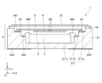
図1は、第1実施形態に係る振動デバイスを示す断面図である。図2は、図1の振動デバイスを示す平面図である。図3は、図1の振動デバイスが有する振動素子を示す平面図である。図4は、図3中のA-A線断面図である。図5は、図3中のB-B線断面図である。図6および図7は、図3の振動素子の駆動を説明する模式図である。図8は、支持基板を上面側から見た斜視図である。図9は、支持基板を下面側から見た斜視図である。
<First Embodiment>
FIG. 1 is a cross-sectional view showing the vibration device according to the first embodiment. 2 is a plan view showing the vibration device of FIG. 1. FIG. 3 is a plan view showing a vibration element included in the vibration device of FIG. 1. FIG. 4 is a cross-sectional view taken along the line AA in FIG. 3. FIG. FIG. 5 is a cross-sectional view taken along line BB in FIG. 6 and 7 are schematic diagrams for explaining the driving of the vibrating element of FIG. 3. FIG. FIG. 8 is a perspective view of the support substrate viewed from the upper surface side. FIG. 9 is a perspective view of the support substrate viewed from the bottom side.
なお、説明の便宜上、図1から図9には、互いに直交する3軸であるA軸、B軸およびC軸を示している。また、以下では、各軸の矢印先端側を「プラス側」とも言い、反対側を「マイナス側」とも言う。また、C軸のプラス側を「上」とも言い、マイナス側を「下」とも言う。また、C軸方向からの平面視を、単に「平面視」とも言う。 For convenience of explanation, FIGS. 1 to 9 show the A-axis, B-axis, and C-axis, which are three axes orthogonal to each other. Also, hereinafter, the arrow tip side of each axis is also called the "plus side", and the opposite side is also called the "minus side". Also, the positive side of the C-axis is also called "upper" and the negative side is also called "lower". A plan view from the C-axis direction is also simply referred to as a “plan view”.
図1に示す振動デバイス1は、C軸を検出軸とする角速度ωcを検出する物理量センサーである。このように、振動デバイス1を物理量センサーとすることにより、振動デバイス1を幅広い電子機器に搭載することができ、高い需要を有する利便性の高い振動デバイス1となる。このような振動デバイス1は、パッケージ2と、パッケージ2に収納されている回路素子3、支持基板4および振動素子6と、を有する。
A
パッケージ2は、上面に開口する凹部211を備えるベース21と、凹部211の開口を塞いでベース21の上面に接合部材23を介して接合されているリッド22と、を有する。パッケージ2の内側には凹部211によって内部空間Sが形成され、内部空間Sに回路素子3、支持基板4および振動素子6がそれぞれ収容されている。例えば、ベース21は、アルミナ等のセラミックスで構成することができ、リッド22は、コバール等の金属材料で構成することができる。ただし、ベース21およびリッド22の構成材料としては、それぞれ、特に限定されない。
The
内部空間Sは、気密であり、減圧状態、好ましくは、より真空に近い状態となっている。これにより、粘性抵抗が減って振動素子6の振動特性が向上する。ただし、内部空間Sの雰囲気は、特に限定されず、例えば、大気圧状態、加圧状態となっていてもよい。
The internal space S is airtight and is in a decompressed state, preferably in a state closer to a vacuum. As a result, the viscous resistance is reduced and the vibration characteristics of the vibrating
また、凹部211は、複数の凹部で構成され、ベース21の上面に開口している凹部211aと、凹部211aの底面に開口し、凹部211aよりも開口幅が小さい凹部211bと、凹部211bの底面に開口し、凹部211bよりも開口幅が小さい凹部211cと、を有する。そして、凹部211aの底面に、振動素子6を支持した状態で支持基板4が固定され、凹部211cの底面に回路素子3が固定されている。
The recessed
また、図2に示すように、内部空間Sにおいて、振動素子6、支持基板4および回路素子3は、平面視で互いに重なって配置されている。言い換えると、振動素子6、支持基板4および回路素子3は、C軸に沿って並んで配置されている。これにより、パッケージ2のA軸方向およびB軸方向への平面的な広がりを抑制でき、振動デバイス1の小型化を図ることができる。また、支持基板4は、振動素子6と回路素子3との間に位置し、振動素子6を下側すなわちC軸マイナス側から支えるように支持している。
Further, as shown in FIG. 2, in the internal space S, the
また、図1および図2に示すように、凹部211aの底面には複数の内部端子241が配置され、凹部211bの底面には複数の内部端子242が配置され、ベース21の下面には複数の外部端子243が配置されている。これら内部端子241、242および外部端子243は、ベース21内に形成されている図示しない配線を介して電気的に接続されている。また、内部端子241は、導電性の接合部材B1、B2および支持基板4を介して振動素子6と電気的に接続され、内部端子242は、ボンディングワイヤーBWを介して回路素子3と電気的に接続されている。
1 and 2, a plurality of
振動素子6は、物理量センサー素子として、C軸を検出軸とする角速度ωcを検出することのできる角速度センサー素子である。図3に示すように、振動素子6は、振動基板7と、振動基板7の表面に配置されている電極8と、を有する。振動基板7は、Zカット水晶基板から構成されている。Zカット水晶基板は、水晶の結晶軸である電気軸としてのX軸および機械軸としてのY軸で規定されるX-Y平面に広がりを有し、光軸としてのZ軸に沿った方向に厚みを有している。
The
振動素子6は、板状であり、支持基板4側の主面である第3面としての下面7aと、下面7aとは反対側の主面である第4面としての上面7bと、を有する。また、振動基板7は、中央部に位置する素子基部70と、素子基部70からB軸方向両側に延出している一対の検出腕71、72と、素子基部70からA軸方向両側に延出している一対の連結腕73、74と、連結腕73の先端部からB軸方向両側に延出している一対の駆動腕75、76と、連結腕74の先端部からB軸方向両側に延出している一対の駆動腕77、78と、を有する。
The vibrating
また、図4および図5に示すように、検出腕71、72および駆動腕75~78は、それぞれ、上面7bと、下面7aと、上面7bと下面7aとを接続する一対の駆動腕側面としての側面7c、7dと、を有する。さらに、駆動腕75~78では、上面7bは、下側に凹没している凹部7eを有し、下面7aは、上側に凹没している凹部7fを有する。すなわち、検出腕71、72は、略矩形の横断面形状をなし、駆動腕75~78は、略H状の横断面形状をなしている。
Further, as shown in FIGS. 4 and 5, the
電極8は、駆動信号電極81と、駆動定電位電極82と、第1検出信号電極83と、検出定電位電極としての第1検出接地電極84と、第2検出信号電極85と、検出定電位電極としての第2検出接地電極86と、を有する。なお、駆動定電位電極82は、駆動信号電極81に対する定電位側の電極であり、低電位に接続されている。なお、駆動定電位電極82は、グランドに接続されていてもよい。第1検出接地電極84は、第1検出信号電極83のグランドであり、第2検出接地電極86は、第2検出信号電極85のグランドである。
The
駆動信号電極81は、駆動腕75、76の両側面7c、7dと、駆動腕77、78の上面7bおよび下面7aと、に配置されている。一方、駆動定電位電極82は、駆動腕75、76の上面7bおよび下面7aと、駆動腕77、78の両側面7c、7dと、に配置されている。また、第1検出信号電極83は、検出腕71の上面7bおよび下面7aに配置され、第1検出接地電極84は、検出腕71の両側面7c、7dに配置されている。一方、第2検出信号電極85は、検出腕72の上面7bおよび下面7aに配置され、第2検出接地電極86は、検出腕72の両側面7c、7dに配置されている。
The
また、これら電極81~86は、それぞれ、素子基部70の下面まで引き回されている。そのため、素子基部70の下面には、駆動信号電極81と電気的に接続されている端子701と、駆動定電位電極82と電気的に接続されている端子702と、第1検出信号電極83と電気的に接続されている端子703と、第1検出接地電極84と電気的に接続されている端子704と、第2検出信号電極85と電気的に接続されている端子705と、第2検出接地電極86と電気的に接続されている端子706と、が配置されている。
Further, these
このような振動素子6は、次のようにして角速度ωcを検出する。まず、駆動信号電極81および駆動定電位電極82間に駆動信号を印加すると、駆動腕75~78が、図6に示すように、A軸およびB軸に平行な平面内に沿って、かつA軸に沿って屈曲振動する。以下、この駆動モードを駆動振動モードと言う。そして、駆動振動モードで駆動している状態で、振動素子6に角速度ωcが加わると、図7に示す検出振動モードが新たに励振される。検出振動モードでは、駆動腕75~78にコリオリの力が作用して矢印Dに示す方向の振動が励振され、この振動に呼応して、検出腕71、72が矢印Eに示す方向に屈曲振動による検出振動が生じる。このような検出振動モードによって検出腕71に発生した電荷を第1検出信号電極83および第1検出接地電極84の間から第1検出信号として取り出し、検出腕72に発生した電荷を第2検出信号電極85および第2検出接地電極86の間から第2検出信号として取り出し、これら第1、第2検出信号に基づいて角速度ωcを検出することができる。
Such a
図1に戻って、回路素子3は、凹部211cの底面に固定されている。回路素子3には、振動素子6を駆動し、振動素子6に加わった角速度ωcを検出する駆動回路および検出回路が含まれている。ただし、回路素子3としては、特に限定されず、例えば、温度補償回路等、他の回路が含まれていてもよい。
Returning to FIG. 1, the
また、支持基板4は、振動素子6側の主面である第1面としての上面4aと、上面4aと反対側の主面である第2面としての下面4bと、を有する板状である。また、図2に示すように、支持基板4は、基部40と、基部40を支持し、基部40を間に挟んでA軸方向両側に分かれて配置されている第1支持部411および第2支持部412を備える支持部41と、基部40と第1支持部411とを接続している一対の梁部42、43と、基部40と第2支持部412とを接続している一対の梁部44、45と、を有する。
Further, the
そして、基部40に導電性の接合部材B2を介して振動素子6の素子基部70が固定されており、第1支持部411および第2支持部412がそれぞれ接合部材B1を介して凹部211aの底面に固定されている。つまり、振動素子6は、支持基板4を介してベース21に固定されている。このように、振動素子6とベース21との間に支持基板4を介在させることにより、支持基板4によってベース21から伝わる応力を吸収、緩和することができ、当該応力が振動素子6に伝わり難くなる。そのため、振動素子6の振動特性の低下や変動を効果的に抑制することができる。
The
特に、本実施形態では、平面視で、第1、第2支持部411、412がそれぞれ振動素子6の外側に位置している。具体的には、振動素子6のA軸プラス側に第1支持部411が位置し、A軸マイナス側に第2支持部412が位置している。これにより、第1、第2支持部411、412を、振動素子6を間に挟んで互いに十分に離間させて配置することができるため、振動素子6をより安定した姿勢で支持することができる。そのため、振動素子6の振動特性が向上する。
In particular, in this embodiment, the first and
なお、接合部材B1、B2としては、導電性と接合性とを兼ね備えていれば、特に限定されず、例えば、金バンプ、銀バンプ、銅バンプ、はんだバンプ等の各種金属バンプ、ポリイミド系、エポキシ系、シリコーン系、アクリル系の各種接着剤に銀フィラー等の導電性フィラーを分散させた導電性接着剤等を用いることができる。接合部材B1、B2として前者の金属バンプを用いると、接合部材B1、B2からのガスの発生を抑制でき、内部空間Sの環境変化、特に圧力の上昇を効果的に抑制することができる。一方、接合部材B1、B2として後者の導電性接着剤を用いると、接合部材B1、B2が比較的柔らかくなり、接合部材B1、B2においても前述の応力を吸収、緩和することができる。 The bonding members B1 and B2 are not particularly limited as long as they have both conductivity and bonding properties. A conductive adhesive obtained by dispersing a conductive filler such as a silver filler in various types of adhesives such as silicone-based, acrylic-based, etc. can be used. When the former metal bumps are used as the bonding members B1 and B2, generation of gas from the bonding members B1 and B2 can be suppressed, and environmental changes in the internal space S, particularly pressure increases, can be effectively suppressed. On the other hand, when the latter conductive adhesive is used as the joint members B1 and B2, the joint members B1 and B2 become relatively soft, and the aforementioned stress can be absorbed and relaxed in the joint members B1 and B2 as well.
本実施形態では、接合部材B1として導電性接着剤を用いており、接合部材B2として金属バンプを用いている。異種の材料である支持基板4とベース21とを接合する接合部材B1として導電性接着剤を用いることにより、これらの間の熱膨張係数の差に起因して生じる熱応力を接合部材B1によって効果的に吸収、緩和することができる。一方、支持基板4と振動素子6とは、比較的狭い領域に配置されている6つの接合部材B2で接合されているため、接合部材B2として金属バンプを用いることにより、導電性接着剤のような濡れ広がりが抑制され、接合部材B2同士の接触を効果的に抑制することができる。
In this embodiment, a conductive adhesive is used as the bonding member B1, and a metal bump is used as the bonding member B2. By using a conductive adhesive as the bonding member B1 for bonding the
図3に示すように、梁部42、43、44、45は、それぞれ、その途中にS字状に蛇行した部分を有し、A軸方向、B軸方向およびC軸方向に弾性変形し易い形状となっている。梁部42~45がA軸方向、B軸方向およびC軸方向に変形することにより、ベース21から伝わる応力を効果的に吸収、緩和することができる。ただし、梁部42~45の形状は、それぞれ、特に限定されず、例えば、蛇行した部分を省略してストレート状としてもよい。また、梁部42~45は、少なくとも1つが他と異なる形状となっていてもよい。
As shown in FIG. 3, the
また、C軸方向からの平面視で、振動素子6の駆動腕75が梁部42と重なり、駆動腕76が梁部43と重なり、駆動腕77が梁部44と重なり、駆動腕78が梁部45と重なっている。そのため、衝撃等によって駆動腕75~78がC軸方向に撓んだ際、駆動腕75~78が梁部42~45と接触し、それ以上の過度な撓みが抑制される。すなわち、梁部42~45が駆動腕75~78のC軸方向への過度な変形を抑制するストッパーとして機能する。これにより、振動素子6の破損を抑制することができる。特に、梁部42~45は、支持基板4の中でも柔らかい部位であるため、駆動腕75~78を梁部42~45に接触させることにより、接触時の衝撃を和らげることもできる。
In a plan view from the C-axis direction, the
また、梁部42、43、44、45は、それぞれ、横断面形状が略矩形であり、上面4aと、下面4bと、上面4aと下面4bとを接続する一対の梁部側面としての側面4c、4dと、を有する。
The
このような支持基板4は、水晶基板で構成されている。このように、支持基板4を振動基板7と同様に水晶基板で構成することにより、支持基板4と振動基板7との熱膨張係数を等しくすることができる。そのため、支持基板4と振動基板7との間には、互いの熱膨張係数差に起因する熱応力が実質的に生じず、振動素子6がより応力を受け難くなる。そのため、振動素子6の振動特性の低下や変動をより効果的に抑制することができる。
Such a
特に、支持基板4は、振動素子6が有する振動基板7と同じカット角の水晶基板で構成されている。本実施形態では、振動基板7がZカット水晶基板で構成されているため、支持基板4もZカット水晶基板で構成されている。また、支持基板4の結晶軸の向きは、振動基板7の結晶軸の向きと一致している。すなわち、支持基板4と振動基板7とでX軸が一致し、Y軸が一致し、Z軸が一致している。水晶は、X軸方向、Y軸方向およびZ軸方向のそれぞれで熱膨張係数が異なるため、支持基板4と振動基板7とを同じカット角とし、互いの結晶軸の向きを揃えることにより、支持基板4と振動基板7との間で前述の熱応力がより生じ難くなる。そのため、振動素子6がさらに応力を受け難くなり、その振動特性の低下や変動をさらに効果的に抑制することができる。
In particular, the
なお、支持基板4としては、これに限定されず、例えば、振動基板7と同じカット角であるが、結晶軸の方向が振動基板7とは異なっていてもよい。また、支持基板4は、振動基板7と異なるカット角の水晶基板から形成されていてもよい。また、支持基板4は、水晶基板から形成されていなくてもよい。この場合、支持基板4の構成材料は、水晶との熱膨張係数の差が、水晶とベース21の構成材料との熱膨張係数差よりも小さい材料であることが好ましい。
Note that the
また、支持基板4には、振動素子6と内部端子241とを電気的に接続している配線5が配置されている。配線5は、端子701と内部端子241とを電気的に接続している駆動信号配線51と、端子702と内部端子241とを電気的に接続している駆動定電位配線52と、端子703と内部端子241とを電気的に接続している検出信号配線としての第1検出信号配線53と、端子704、706と内部端子241とを電気的に接続している検出定電位配線としての検出接地配線54と、端子705と内部端子241とを電気的に接続している検出信号配線としての第2検出信号配線55と、を有する。
図8および図9に示すように、駆動信号配線51は、その一端部に位置し、基部40の上面4aに配置されている端子511と、その他端部に位置し、第2支持部412の下面4bに配置されている端子512と、端子511、512を電気的に接続している配線513と、を有する。また、配線513は、梁部44、45の下面4bを通って基部40と第2支持部412とに引き回されて、端子511、512を電気的に接続している。なお、梁部44の下面4bは、幅方向に略二分されている2つの領域Q41、Q42を有し、同様に、梁部45の下面4bは、幅方向に略二分されている2つの領域Q51、Q52を有する。そして、配線513は、梁部44の下面4bの領域Q41内を通って基部40と第2支持部412とに引き回され、梁部45の下面4bの領域Q51内を通って基部40と第2支持部412とに引き回されている。
As shown in FIGS. 8 and 9, the
駆動定電位配線52は、その一端部に位置し、基部40の上面4aに配置されている端子521と、その他端部に位置し、第1支持部411の下面4bに配置されている端子522と、端子521、522を電気的に接続している配線523と、を有する。また、配線523は、梁部42、43の下面4bを通って基部40と第1支持部411とに引き回されて、端子521、522を電気的に接続している。なお、梁部42の下面4bは、幅方向に略二分されている2つの領域Q21、Q22を有し、同様に、梁部43の下面4bは、幅方向に略二分されている2つの領域Q31、Q32を有する。そして、配線523は、梁部42の下面4bの領域Q21内を通って基部40と第1支持部411とに引き回され、梁部43の下面4bの領域Q31内を通って基部40と第1支持部411とに引き回されている。
The drive constant
第1検出信号配線53は、その一端部に位置し、基部40の上面4aに配置されている端子531と、その他端部に位置し、第1支持部411の下面4bに配置されている端子532と、端子531、532を電気的に接続している配線533と、を有する。また、配線533は、梁部43の下面4bを通って基部40と第1支持部411とに引き回されて、端子531、532を電気的に接続している。なお、前述したように、梁部43の下面4bは、幅方向に略二分されている2つの領域Q31、Q32を有する。そして、配線533は、梁部43の下面4bの領域Q32内を通って基部40と第1支持部411とに引き回されている。つまり、梁部43の下面4bには、配線533、523が梁部43の幅方向に並んで配置されている。
The first
第2検出信号配線55は、その一端部に位置し、基部40の上面4aに配置されている端子551と、その他端部に位置し、第1支持部411の下面4bに配置されている端子552と、端子551、552を電気的に接続している配線553と、を有する。また、配線553は、梁部42の下面4bを通って基部40と第1支持部411とに引き回されて端子551、552を電気的に接続している。なお、前述したように、梁部42の下面4bは、幅方向に略二分されている2つの領域Q21、Q22を有する。そして、配線553は、梁部42の下面4bの領域Q22内を通って基部40と第1支持部411とに引き回されている。つまり、梁部42の下面4bには、配線553、523が梁部42の幅方向に並んで配置されている。
The second
検出接地配線54は、その一端部に位置し、基部40の上面4aに配置されている端子541と、その他端部に位置し、第2支持部412の下面4bに配置されている一対の端子542と、端子541、542を電気的に接続している配線543と、を有する。配線543は、他の配線51、52、53、55と電気的な絶縁状態を確保したうえで、支持基板4の配線51、52、53、55から露出している部分のなるべく広範囲を覆うように配置されている。以下、詳細に説明する。
The
基部40では、配線543は、他の配線51、52、53、55と電気的な絶縁状態を保った上で、基部40の上面4a、側面および下面4bの広範囲にわたって配置されている。また、第1、第2支持部411、412では、配線543は、他の配線51、52、53、55と電気的な絶縁状態を保った上で、第1、第2支持部411、412の上面4aのほぼ全域にわたって配置されている。
In the
また、梁部42では、配線543は、他の配線52、55と電気的な絶縁状態を保った上で、梁部42の上面4a、両側面4c、4dおよび下面4bの幅方向両端部にわたって配置されている。また、梁部43では、配線543は、他の配線52、53と電気的な絶縁状態を保った上で、梁部43の上面4a、両側面4c、4dおよび下面4bの幅方向両端部にわたって配置されている。また、梁部44では、配線543は、他の配線51と電気的な絶縁状態を保った上で、梁部44の上面4a、両側面4c、4d、下面4bの幅方向両端部および領域Q42にわたって配置されている。また、梁部45では、配線543は、他の配線51と電気的な絶縁状態を保った上で、梁部45の上面4a、両側面4c、4d、下面4bの幅方向両端部および領域Q52にわたって配置されている。
In addition, in the
検出接地配線54をこのように配置することにより、次の効果を発揮することができる。梁部43では、第1検出信号電極83と電気的に接続されている配線533が下面4bに配置されており、第1、第2検出接地電極84、86と電気的に接続されている配線543が上面4aに配置されている。このような配置とすることにより、振動素子6と配線533との間に配線543が位置する。同様に、梁部42では、第2検出信号電極85と電気的に接続されている配線553が下面4bに配置されており、第1、第2検出接地電極84、86と電気的に接続されている配線543が上面4aに配置されている。このような配置とすることにより、振動素子6と配線553との間に配線543が位置する。
By arranging the
配線543は、グランドすなわち定電位に接続されているため、シールド層として機能し、これにより、振動素子6に配置されている駆動信号電極81と配線533、553とのノイズ干渉を抑制することができる。そのため、配線533、553を介して、駆動信号電極81に印加される駆動信号がノイズとして検出信号に混入するのを効果的に抑制することができる。そのため、S/N比の高い高精度な検出信号を回路素子3に送信することができ、角速度ωcをより高精度に検出することができる。
Since the
特に、本実施形態では、梁部42、43において、その上面4aのみならず、両側面4c、4dおよび下面4bにわたって配線543が配置されている。すなわち、配線533、553の周囲を囲むようにして配線543が配置されている。そのため、上述したシールド効果がより高まり、駆動信号電極81と配線533、553とのノイズ干渉をより効果的に抑制することができる。また、梁部42、43の下面4bには配線533、553の他にも駆動定電位電極82と電気的に接続されている配線523が配置されている。配線523は、定電位に接続されているため、シールド層として機能する。そのため、配線523によっても、駆動信号電極81と配線533、553とのノイズ干渉を抑制することができる。なお、配線523は、グランドに接続されていてもよい。
In particular, in this embodiment, in the
また、C軸方向からの平面視で、配線533が配置されている梁部43は、駆動腕76と交差しており、駆動腕76と対向している部分すなわち重なっている部分を有する。また、C軸方向からの平面視で、配線553が配置されている梁部42は、駆動腕75と交差しており、駆動腕75と重なる部分を有する。そのため、梁部42、43に配置されている配線533、553と駆動腕75、76に配置されている駆動信号電極81とが近接し、前述したノイズ干渉が非常に生じ易い。このような位置関係の中で、梁部42、43の上面4aすなわち駆動信号電極81と配線533、553との間にシールド層として機能する配線543を配置することにより、前述したノイズ干渉抑制効果をより顕著に発揮することができる。
Further, the
特に、C軸方向からの平面視で梁部42、43と重なる駆動腕75、76は、両側面7c、7dに駆動信号電極81が配置されており、下面7aおよび上面7bに駆動定電位電極82が配置されている。つまり、駆動信号電極81は、配線533、553に対して横を向いている。そのため、梁部42、43を迂回して第1、第2検出信号配線53、55との間に容量結合が形成され易い。したがって、梁部42、43の上面4aすなわち駆動信号電極81と配線533、553との間にシールド層として機能する配線543を配置することにより、駆動信号電極81と第1、第2検出信号配線53、55とのノイズ干渉抑制効果をさらに顕著に発揮することができる。
In particular, the
また、第1、第2支持部411、412の上面4aにも配線543が配置されているため、配線543がより広範囲にわたって配置され、前述したノイズ干渉抑制効果をさらに顕著に発揮することができる。また、配線543を支持基板4の広範囲にわたって配置することにより、例えば、駆動信号電極81と回路素子3とのノイズ干渉を効果的に抑制することもできる。
In addition, since the
以上、振動デバイス1について説明した。このような振動デバイス1は、前述したように、振動素子6と、振動素子6と対向して配置され、振動素子6側の第1面としての上面4aおよび上面4aと反対側の第2面としての下面4bを備え、振動素子6を支持している支持基板4と、を有する。また、振動素子6は、駆動信号電極81および駆動定電位電極82を備え、駆動信号電極81に駆動信号を印加することにより駆動振動する駆動腕75、76、77、78と、検出信号電極としての第1、第2検出信号電極83、85および検出定電位電極としての第1、第2検出接地電極84、86を備え、検出対象の物理量である角速度ωcを受けて検出振動することにより第1、第2検出信号電極83、85から検出信号が出力される検出腕71、72と、を有する。
The
また、支持基板4は、振動素子6を支持している基部40と、基部40を支持している支持部としての第1、第2支持部411、412と、基部40と第1、第2支持部411、412とを接続している複数の梁部42、43、44、45と、駆動信号電極81と電気的に接続されており、少なくとも1つの梁部、本実施形態では梁部44、45を通って基部40と第2支持部412とに引き回されている駆動信号配線51と、駆動定電位電極82と電気的に接続されており、少なくとも1つの梁部、本実施形態では梁部42、43を通って基部40と第1支持部411とに引き回されている駆動定電位配線52と、第1検出信号電極83と電気的に接続されており、少なくとも1つの梁部、本実施形態では梁部43を通って基部40と第1支持部411とに引き回されている検出信号配線としての第1検出信号配線53と、第2検出信号電極85と電気的に接続されており、少なくとも1つの梁部、本実施形態では梁部42を通って基部40と第1支持部411とに引き回されている検出信号配線としての第2検出信号配線55と、第1、第2検出接地電極84、86と電気的に接続されており、少なくとも1つの梁部、本実施形態では梁部42~45を通って基部40と第1、第2支持部411、412とに引き回されている検出定電位配線としての検出接地配線54と、を有する。
Further, the
そして、複数の梁部42~45に含まれる所定の梁部43では、上面4aに検出接地配線54が配置され、下面4bに第1検出信号配線53が配置されており、複数の梁部42~45に含まれる所定の梁部42では、上面4aに検出接地配線54が配置され、下面4bに第2検出信号配線55が配置されている。
A
このような構成によれば、梁部43において、振動素子6と第1検出信号配線53との間に検出接地配線54が位置する。同様に、梁部42において、振動素子6と第2検出信号配線55との間に検出接地配線54が位置する。検出接地配線54は、グランドすなわち定電位に接続されているため、シールド層として機能し、これにより、振動素子6に配置されている駆動信号電極81と支持基板4に配置されている第1、第2検出信号配線53、55とのノイズ干渉を抑制することができる。したがって、振動デバイス1によれば、第1、第2検出信号配線53、55を介して、駆動信号電極81に印加される駆動信号がノイズとして検出信号に混入するのを効果的に抑制することができる。そのため、S/N比の高い高精度な検出信号を取得することができ、角速度ωcをより高精度に検出することができる。
According to such a configuration, the
また、前述したように、所定の梁部42、43は、上面4aと下面4bとを接続する一対の梁部側面としての側面4c、4dを有する。そして、所定の梁部42、43において、検出接地配線54は、上面4a、各側面4c、4dおよび下面4bに配置されている。このような配置とすることにより、配線533、553の周囲を囲むようにして配線543を配置することができる。そのため、上述したシールド効果がより高まり、駆動信号電極81と配線533、553とのノイズ干渉をより効果的に抑制することができる。
Further, as described above, the
また、前述したように、所定の梁部42は、駆動腕75と対向している部分を有し、所定の梁部43は、駆動腕76と対向している部分を有する。そのため、梁部42、43に配置されている配線533、553と駆動腕75、76に配置されている駆動信号電極81とが近接し、前述したノイズ干渉が非常に生じ易い。このような位置関係の中で、梁部42、43の上面4aすなわち駆動信号電極81と配線533、553との間にシールド層として機能する検出接地配線54を配置することにより、前述したノイズ干渉抑制効果をより顕著に発揮することができる。
Further, as described above, the
また、前述したように、駆動腕75、76は、支持基板4側の第3面である下面7aと、下面7aと反対側の第4面である上面7bと、下面7aと上面7bとを接続する一対の側面7c、7dと、を有する。そして、下面7aおよび上面7bに駆動定電位電極82が配置され、各側面7c、7dに駆動信号電極81が配置されている。このような構成では、梁部42、43を迂回して第1、第2検出信号配線53、55との間に容量結合が形成され易い。したがって、梁部42、43の上面4aすなわち駆動信号電極81と配線533、553との間にシールド層として機能する配線543を配置することにより、駆動信号電極81と第1、第2検出信号配線53、55とのノイズ干渉抑制効果をさらに顕著に発揮することができる。
Further, as described above, the driving
また、前述したように、第1、第2支持部411、412の上面4aには検出接地配線54が配置されている。これにより、支持基板4上において、検出接地配線54をより広範囲にわたって配置することができる。そのため、前述したノイズ干渉抑制効果をさらに顕著に発揮することができる。
Further, as described above, the
また、前述したように、互いに直交する3軸をA軸、B軸およびC軸とし、C軸方向に振動素子6と支持基板4とが対向しているとしたとき、振動素子6は、素子基部70と、素子基部70からB軸方向両側に延出している一対の検出腕71、72と、素子基部70からA軸方向両側に延出している一対の連結腕73、74と、連結腕73の先端部からB軸方向両側に延出している一対の駆動腕75、76と、連結腕74の先端部からB軸方向両側に延出している一対の駆動腕77、78と、を有し、素子基部70が接合部材B2を介して基部40に固定されている。これにより、角速度ωcを精度よく検出することのできる振動素子6となる。
Further, as described above, when the three mutually orthogonal axes are the A axis, the B axis, and the C axis, and the vibrating
また、前述したように、振動デバイス1は、振動素子6と電気的に接続されている回路素子3を有する。そして、振動素子6と回路素子3との間に支持基板4が位置している。このような構成によれば、支持基板4に配置されている検出接地配線54や駆動定電位配線52がシールド層として機能し、振動素子6と回路素子3とのノイズ干渉を効果的に抑制することができる。
Further, as described above, the vibrating
<第2実施形態>
図10は、第2実施形態の振動デバイスが有する支持基板を上側から見た斜視図である。図11は、図10に示す支持基板を下側から見た斜視図である。
<Second embodiment>
FIG. 10 is a perspective view of the supporting substrate of the vibrating device of the second embodiment, viewed from above. FIG. 11 is a perspective view of the support substrate shown in FIG. 10 as seen from below.
本実施形態は、振動素子6が異なること以外は、前述した第1実施形態と同様である。なお、以下の説明では、本実施形態に関し、前述した実施形態との相違点を中心に説明し、同様の事項に関してはその説明を省略する。また、図10および図11において、前述した実施形態と同様の構成については、同一符号を付している。
This embodiment is the same as the first embodiment described above, except that the
図10および図11に示すように、駆動信号電極81は、駆動腕75、76の上面7bおよび下面7aと、駆動腕77、78の両側面7c、7dと、に配置されている。一方、駆動定電位電極82は、駆動腕75、76の両側面7c、7dと、駆動腕77、78の上面7bおよび下面7aと、に配置されている。
As shown in FIGS. 10 and 11, the
つまり、C軸方向からの平面視で梁部42、43と重なる駆動腕75、76は、下面7aおよび上面7bに駆動信号電極81が配置され、両側面7c、7dに駆動定電位電極82が配置されている。そのため、駆動信号電極81は、配線533、553側を向き、前述した第1実施形態の駆動腕75、76のようにその両側面7c、7dに駆動信号電極81が配置されている場合と比べて、第1、第2検出信号配線53、55との間に容量結合が形成され易い場合もある。したがって、梁部42、43の上面4aすなわち駆動信号電極81と配線533、553との間にシールド層として機能する配線543を配置することにより、駆動信号電極81と第1、第2検出信号配線53、55とのノイズ干渉抑制効果をさらに顕著に発揮することができる。
That is, the driving
以上のように、駆動腕75、76は、支持基板4側の第3面である下面7aと、下面7aと反対側の第4面である上面7bと、下面7aと上面7bとを接続する一対の駆動腕側面である側面7c、7dと、を有する。そして、下面7aおよび上面7bに駆動信号電極81が配置され、各側面7c、7dに駆動定電位電極82が配置されている。そのため、下面7aに配置されている駆動信号電極81が支持基板4側を向き、駆動信号電極81と第1、第2検出信号配線53、55とのノイズ干渉が生じ易い。したがって、梁部42、43の上面4aすなわち駆動信号電極81と第1、第2検出信号配線53、55との間にシールド層として機能する検出接地配線54を配置することにより、前述したノイズ干渉抑制効果をさらに顕著に発揮することができる。
As described above, the driving
このような第2実施形態によっても、前述した第1実施形態と同様の効果を発揮することができる。 Such a second embodiment can also exhibit the same effect as the first embodiment described above.
<第3実施形態>
図12は、第3実施形態の振動デバイスが有する支持基板を上側から見た斜視図である。図13は、図12に示す支持基板を下側から見た斜視図である。
<Third Embodiment>
FIG. 12 is a perspective view of the supporting substrate of the vibrating device of the third embodiment, viewed from above. FIG. 13 is a perspective view of the support substrate shown in FIG. 12 as seen from below.
本実施形態は、支持基板4の構成が異なること以外は、前述した第1実施形態と同様である。なお、以下の説明では、本実施形態に関し、前述した実施形態との相違点を中心に説明し、同様の事項に関してはその説明を省略する。また、図12および図13において、前述した実施形態と同様の構成については、同一符号を付している。
This embodiment is the same as the first embodiment described above, except that the configuration of the
図12および図13に示すように、駆動信号配線51の配線513は、梁部44、45の下面4bを通って基部40と第2支持部412とに引き回されて、端子511、512を電気的に接続している。また、第1検出信号配線53の配線533は、梁部43の下面4bを通って基部40と第1支持部411とに引き回されて、端子531、532を電気的に接続している。また、第2検出信号配線55の配線553は、梁部42の下面4bを通って基部40と第1支持部411とに引き回されて端子551、552を電気的に接続している。これら駆動信号配線51、第1検出信号配線53および第2検出信号配線55の配置は、前述した第1実施形態と同様である。
As shown in FIGS. 12 and 13, the
一方、駆動定電位配線52の配線523および検出接地配線54の配線543は、前述した第1実施形態と異なる配置となっており、他の配線51、52、53、55と電気的な絶縁状態を確保したうえで、支持基板4の配線51、52、53、55から露出している部分のなるべく広範囲を覆うように配置されている。以下、詳細に説明する。
On the other hand, the
基部40では、配線543が、他の配線51、52、53、55と電気的な絶縁状態を保った上で、基部40の上面4a、側面および下面4bの広範囲にわたって配置されている。また、第1支持部411では、配線523が、他の配線51、52、53、55と電気的な絶縁状態を保った上で、第1支持部411の上面4aのほぼ全域にわたって配置されている。一方、第2支持部412では、配線543が、他の配線51、52、53、55と電気的な絶縁状態を保った上で、第2支持部412の上面4aのほぼ全域にわたって配置されている。
In the
また、梁部42では、配線523が、他の配線55と電気的な絶縁状態を保った上で、梁部42の上面4a、両側面4c、4dおよび下面4bの幅方向両端部にわたって配置されている。また、梁部43では、配線523が、他の配線53と電気的な絶縁状態を保った上で、梁部43の上面4a、両側面4c、4dおよび下面4bの幅方向両端部にわたって配置されている。また、梁部44では、配線543が、他の配線51と電気的な絶縁状態を保った上で、梁部44の上面4a、両側面4c、4dおよび下面4bの幅方向両端部にわたって配置されている。また、梁部45では、配線543が、他の配線51と電気的な絶縁状態を保った上で、梁部45の上面4a、両側面4c、4dおよび下面4bの幅方向両端部にわたって配置されている。
In addition, in the
このような構成によれば、駆動腕75、76に配置されている駆動信号電極81と、梁部42、43の下面4bに配置されている第1、第2検出信号配線53、55との間に駆動定電位配線52を配置することができる。駆動定電位配線52は、定電位に接続されているため、シールド層として機能する。そのため、振動素子6に配置されている駆動信号電極81と梁部42、43に配置されている第1、第2検出信号配線53、55とのノイズ干渉を抑制することができる。したがって、S/N比の高い高精度な検出信号を回路素子3に送信することができ、角速度ωcをより高精度に検出することができる。なお、駆動定電位配線52は、検出接地配線54と同様に、グランドに接続されていてもよい。
According to such a configuration, the
以上のように、複数の梁部42~45に含まれる所定の梁部43では、上面4aに駆動定電位配線52が配置され、下面4bに第1検出信号配線53が配置されており、複数の梁部42~45に含まれる所定の梁部42では、上面4aに駆動定電位配線52が配置され、下面4bに第2検出信号配線55が配置されている。
As described above, in the
このような構成によれば、梁部43において、振動素子6と第1検出信号配線53との間に駆動定電位配線52が位置する。同様に、梁部42において、振動素子6と第2検出信号配線55との間に駆動定電位配線52が位置する。駆動定電位配線52は、定電位に接続されているため、シールド層として機能し、これにより、振動素子6に配置されている駆動信号電極81と支持基板4に配置されている第1、第2検出信号配線53、55とのノイズ干渉を抑制することができる。したがって、振動デバイス1によれば、第1、第2検出信号配線53、55を介して、駆動信号電極81に印加される駆動信号がノイズとして検出信号に混入するのを効果的に抑制することができる。そのため、S/N比の高い高精度な検出信号を取得することができ、角速度ωcをより高精度に検出することができる。
According to such a configuration, the driving constant
このような第3実施形態によっても、前述した第1実施形態と同様の効果を発揮することができる。 Such a third embodiment can also exhibit the same effect as the first embodiment described above.
<第4実施形態>
図14は、第4実施形態の振動デバイスが有する支持基板を上側から見た斜視図である。
<Fourth Embodiment>
FIG. 14 is a perspective view of the supporting substrate of the vibrating device of the fourth embodiment, viewed from above.
本実施形態は、支持基板4の構成が異なること以外は、前述した第1実施形態と同様である。なお、以下の説明では、本実施形態に関し、前述した実施形態との相違点を中心に説明し、同様の事項に関してはその説明を省略する。また、図14において、前述した実施形態と同様の構成については、同一符号を付している。
This embodiment is the same as the first embodiment described above, except that the configuration of the
図14に示すように、支持部41は、C軸方向の平面視で、基部40を囲む枠状である。そして、枠状の支持部41の上面4aのほぼ全域には、駆動定電位配線52の配線523および検出接地配線54の配線543が配置されている。このような構成とすることにより、例えば、前述した第1実施形態と比べて、検出接地配線54の面積が大きくなり、その分、駆動信号電極81と第1、第2検出信号配線53、55とのノイズ干渉や、駆動信号電極81と回路素子3とのノイズ干渉を効果的に抑制することができる。
As shown in FIG. 14 , the
このような第4実施形態によっても、前述した第1実施形態と同様の効果を発揮することができる。 Such a fourth embodiment can also exhibit the same effect as the first embodiment described above.
<第5実施形態>
図15は、第5実施形態の振動デバイスを示す平面図である。
<Fifth Embodiment>
FIG. 15 is a plan view showing the vibration device of the fifth embodiment.
本実施形態は、振動素子6の向きが異なること以外は、前述した第1実施形態と同様である。なお、以下の説明では、本実施形態に関し、前述した実施形態との相違点を中心に説明し、同様の事項に関してはその説明を省略する。また、図15において、前述した実施形態と同様の構成については、同一符号を付している。
This embodiment is the same as the above-described first embodiment except that the orientation of the
図15に示すように、本実施形態の振動デバイス1では、振動素子6が第1実施形態からC軸まわりに90°回転して配置されている。
As shown in FIG. 15, in the vibrating
このような第5実施形態によっても、前述した第1実施形態と同様の効果を発揮することができる。 Such a fifth embodiment can also exhibit the same effect as the first embodiment described above.
<第6実施形態>
図16は、第6実施形態の振動デバイスを示す断面図である。
<Sixth Embodiment>
FIG. 16 is a cross-sectional view showing the vibration device of the sixth embodiment.
本実施形態は、振動素子6の配置が異なること以外は、前述した第1実施形態と同様である。なお、以下の説明では、本実施形態に関し、前述した実施形態との相違点を中心に説明し、同様の事項に関してはその説明を省略する。また、図16において、前述した実施形態と同様の構成については、同一符号を付している。
This embodiment is the same as the first embodiment described above, except that the arrangement of the
図16に示すように、振動素子6は、支持基板4と回路素子3との間に配置されている。つまり、振動素子6は、支持基板4の下側に位置し、支持基板4に吊られて支持されている。このような構成によれば、支持基板4と回路素子3との間のスペースに振動素子6を配置することができるため、その分、振動デバイス1の小型化、特に薄型化を図ることができる。ただし、例えば、回路素子3と振動素子6とのノイズ干渉を支持基板4で抑制することができない点において、前述した第1実施形態と比べてノイズ抑制効果が若干低減するおそれがある。
As shown in FIG. 16, the
このような第6実施形態によっても、前述した第1実施形態と同様の効果を発揮することができる。 Such a sixth embodiment can also exhibit the same effect as the first embodiment described above.
<第7実施形態>
図17は、第7実施形態の振動デバイスが有する支持基板を示す断面図である。
<Seventh Embodiment>
FIG. 17 is a cross-sectional view showing a support substrate included in the vibration device of the seventh embodiment.
本実施形態は、回路素子3の配置が異なること以外は、前述した第6実施形態と同様である。なお、以下の説明では、本実施形態に関し、前述した実施形態との相違点を中心に説明し、同様の事項に関してはその説明を省略する。また、図17において、前述した実施形態と同様の構成については、同一符号を付している。
This embodiment is the same as the sixth embodiment described above, except that the arrangement of the
図17に示すように、本実施形態の振動デバイス1では、回路素子3が凹部211aの底面に導電性の接合部材B3を介して固定されており、回路素子3の下面に支持基板4が接合部材B1を介して固定されており、支持基板4の下面に接合部材B2を介して振動素子6が固定されている。このように、振動素子6とベース21との間に支持基板4および回路素子3を介在させることにより、支持基板4および回路素子3によってベース21から伝わる応力を吸収、緩和することができ、当該応力が振動素子6に伝わり難くなる。そのため、振動素子6の振動特性の低下や変動を効果的に抑制することができる。また、本実施形態によれば、凹部211a内に回路素子3を配置することができるため、前述した第1実施形態のように凹部211c内に回路素子3を配置する場合と比べて、回路素子3を大きくすることができる。
As shown in FIG. 17, in the
このような第7実施形態によっても、前述した第1実施形態と同様の効果を発揮することができる。 Such a seventh embodiment can also exhibit the same effect as the first embodiment described above.
<第8実施形態>
図18は、第8実施形態のパーソナルコンピューターを示す斜視図である。
<Eighth Embodiment>
FIG. 18 is a perspective view showing the personal computer of the eighth embodiment.
図18に示す電子機器としてのパーソナルコンピューター1100は、キーボード1102を備えた本体部1104と、表示部1108を備えた表示ユニット1106と、により構成され、表示ユニット1106は、本体部1104に対しヒンジ構造部を介して回動可能に支持されている。また、パーソナルコンピューター1100には、物理量センサーとしての振動デバイス1と、振動デバイス1からの出力信号に基づいて信号処理すなわち各部の制御を行う信号処理回路1110と、が内蔵されている。
A
このように、電子機器としてのパーソナルコンピューター1100は、振動デバイス1と、振動デバイス1の出力信号に基づいて信号処理を行う信号処理回路1110と、を備える。そのため、前述した振動デバイス1の効果を享受でき、高い信頼性を発揮することができる。
As described above, the
<第9実施形態>
図19は、第9実施形態の携帯電話機を示す斜視図である。
<Ninth Embodiment>
FIG. 19 is a perspective view showing a mobile phone according to the ninth embodiment.
図19に示す電子機器としての携帯電話機1200は、図示しないアンテナ、複数の操作ボタン1202、受話口1204および送話口1206を備え、操作ボタン1202と受話口1204との間には、表示部1208が配置されている。また、携帯電話機1200には、物理量センサーとしての振動デバイス1と、振動デバイス1からの出力信号に基づいて信号処理すなわち各部の制御を行う信号処理回路1210と、が内蔵されている。
A
このように、電子機器としての携帯電話機1200は、振動デバイス1と、振動デバイス1の出力信号に基づいて信号処理を行う信号処理回路1210と、を備える。そのため、前述した振動デバイス1の効果を享受でき、高い信頼性を発揮することができる。
As described above, the
<第10実施形態>
図20は、第10実施形態のデジタルスチールカメラを示す斜視図である。
<Tenth Embodiment>
FIG. 20 is a perspective view showing the digital still camera of the tenth embodiment.
図20に示す電子機器としてのデジタルスチールカメラ1300は、ケース1302を備え、このケース1302の背面には表示部1310が設けられている。表示部1310は、CCDによる撮像信号に基づいて表示を行う構成となっており、被写体を電子画像として表示するファインダーとして機能する。また、ケース1302の正面側には、光学レンズやCCDなどを含む受光ユニット1304が設けられている。そして、撮影者が表示部1310に表示された被写体像を確認し、シャッターボタン1306を押すと、その時点におけるCCDの撮像信号が、メモリー1308に転送・格納される。また、デジタルスチールカメラ1300には、物理量センサーとしての振動デバイス1と、振動デバイス1からの出力信号に基づいて信号処理すなわち各部の制御を行う信号処理回路1312と、が内蔵されている。
A
このように、電子機器としてのデジタルスチールカメラ1300は、振動デバイス1と、振動デバイス1の出力信号に基づいて信号処理を行う信号処理回路1312と、を備える。そのため、前述した振動デバイス1の効果を享受でき、高い信頼性を発揮することができる。
As described above, the
なお、振動デバイス1を備える電子機器は、前述したパーソナルコンピューター1100、携帯電話機1200およびデジタルスチールカメラ1300の他、例えば、スマートフォン、タブレット端末、スマートウォッチを含む時計、インクジェット式吐出装置、例えばインクジェットプリンター、HMD(ヘッドマウントディスプレイ)、スマートグラス等のウェアラブル端末、テレビ、ビデオカメラ、ビデオテープレコーダー、カーナビゲーション装置、ページャ、電子手帳、電子辞書、電子翻訳器、電卓、電子ゲーム機器、トレーニング機器、ワードプロセッサー、ワークステーション、テレビ電話、防犯用テレビモニター、電子双眼鏡、POS端末、電子体温計、血圧計、血糖計、心電図計測装置、超音波診断装置、電子内視鏡のような医療機器、魚群探知機、各種測定機器、車両、航空機、船舶に搭載される計器類、携帯端末用の基地局、フライトシミュレーター等であってもよい。
In addition to the
<第11実施形態>
図21は、第11実施形態の自動車を示す斜視図である。
<Eleventh Embodiment>
FIG. 21 is a perspective view showing the automobile of the eleventh embodiment.
図21に示す移動体としての自動車1500は、エンジンシステム、ブレーキシステム、操舵システム、姿勢制御システムおよびキーレスエントリーシステム等のシステム1502を含んでいる。また、自動車1500には、物理量センサーとしての振動デバイス1と、振動デバイス1からの出力信号に基づいて信号処理すなわちシステム1502の制御を行う信号処理回路1510と、が内蔵されている。
An
このように、移動体としての自動車1500は、振動デバイス1と、振動デバイス1の出力信号に基づいて信号処理を行う信号処理回路1510と、を備える。そのため、前述した振動デバイス1の効果を享受でき、高い信頼性を発揮することができる。
As described above, the
なお、振動デバイス1を備える移動体は、自動車1500の他、例えば、ロボット、ドローン、電動車いす、二輪車、航空機、ヘリコプター、船舶、電車、モノレール、貨物運搬用カーゴ、ロケット、宇宙船等であってもよい。
In addition to the
以上、本発明の振動デバイス、電子機器および移動体について、図示の実施形態に基づいて説明したが、本発明はこれに限定されるものではなく、各部の構成は、同様の機能を有する任意の構成のものに置換することができる。また、本発明に、他の任意の構成物が付加されていてもよい。また、各実施形態を適宜組み合わせてもよい。 As described above, the vibration device, the electronic device, and the moving body of the present invention have been described based on the illustrated embodiments, but the present invention is not limited to this, and the configuration of each part can be any arbitrary device having similar functions. It can be replaced with a configuration. Also, other optional components may be added to the present invention. Further, each embodiment may be combined as appropriate.
1…振動デバイス、2…パッケージ、21…ベース、211、211a、211b、211c…凹部、22…リッド、23…接合部材、241、242…内部端子、243…外部端子、3…回路素子、4…支持基板、4a…上面、4b…下面、4c、4d…側面、40…基部、41…支持部、411…第1支持部、412…第2支持部、42、43、44、45…梁部、5…配線、51…駆動信号配線、511、512…端子、513…配線、52…駆動定電位配線、521、522…端子、523…配線、53…第1検出信号配線、531、532…端子、533…配線、54…検出接地配線、541、542…端子、543…配線、55…第2検出信号配線、551、552…端子、553…配線、6…振動素子、7…振動基板、7a…下面、7b…上面、7c、7d…側面、7e、7f…凹部、70…素子基部、701~706…端子、71、72…検出腕、73、74…連結腕、75、76、77、78…駆動腕、8…電極、81…駆動信号電極、82…駆動定電位電極、83…第1検出信号電極、84…第1検出接地電極、85…第2検出信号電極、86…第2検出接地電極、1100…パーソナルコンピューター、1102…キーボード、1104…本体部、1106…表示ユニット、1108…表示部、1110…信号処理回路、1200…携帯電話機、1202…操作ボタン、1204…受話口、1206…送話口、1208…表示部、1210…信号処理回路、1300…デジタルスチールカメラ、1302…ケース、1304…受光ユニット、1306…シャッターボタン、1308…メモリー、1310…表示部、1312…信号処理回路、1500…自動車、1502…システム、1510…信号処理回路、B1、B2、B3…接合部材、BW…ボンディングワイヤー、D、E…矢印、Q21、Q22、Q31、Q32、Q41、Q42、Q51、Q52…領域、S…内部空間、ωc…角速度
DESCRIPTION OF
Claims (13)
前記振動素子と対向し、前記振動素子側の第1面及び前記第1面と反対側の第2面を含み、前記振動素子を支持している支持基板と、
を含み、
前記振動素子は、素子基部と、駆動腕と、検出腕と、を含み、
前記支持基板は、前記素子基部が固定されている基部と、梁部を介して前記基部と接続されている支持部と、を含み、
平面視で、前記駆動腕は、前記梁部と重なり、
前記駆動腕は、駆動信号電極と、駆動定電位電極と、を含み、
前記検出腕は、検出信号電極と、検出定電位電極と、を含み、
前記梁部は、
前記第1面側に前記駆動定電位電極及び前記検出定電位電極の少なくとも何れかに電気的に接続されている定電位配線が配置され、
前記第2面側に前記駆動信号電極及び前記検出信号電極の少なくとも何れかに電気的に接続されている信号配線が配置されていることを特徴とする振動デバイス。 a vibrating element;
a support substrate facing the vibration element , including a first surface on the side of the vibration element and a second surface opposite to the first surface, and supporting the vibration element;
including
the vibration element includes an element base, a drive arm, and a detection arm;
The support substrate includes a base to which the element base is fixed, and a support connected to the base via a beam,
In plan view, the drive arm overlaps the beam,
the drive arm includes a drive signal electrode and a drive constant potential electrode;
The detection arm includes a detection signal electrode and a detection constant potential electrode,
The beam portion
A constant potential wiring electrically connected to at least one of the drive constant potential electrode and the detection constant potential electrode is arranged on the first surface side,
A vibrating device according to claim 1, wherein a signal wiring electrically connected to at least one of the drive signal electrode and the detection signal electrode is arranged on the second surface side.
前記支持部は、第1支持部と、第2支持部と、を含み、
平面視で、前記基部は、前記第1支持部と、前記第2支持部と、の間に配置され、
前記梁部は、
前記基部と、前記第1支持部と、を接続している第1梁部と、
前記基部と、前記第2支持部と、を接続している第2梁部と、
を含むことを特徴とする振動デバイス。 In claim 1,
The support includes a first support and a second support,
In plan view, the base is arranged between the first support and the second support,
The beam portion
a first beam connecting the base and the first support;
a second beam connecting the base and the second support;
A vibration device comprising :
前記第1梁部及び前記第2梁部の前記第1面側に前記検出定電位電極に電気的に接続されている検出定電位配線が配置されていることを特徴とする振動デバイス。 In claim 2,
A vibrating device according to claim 1, wherein detection constant-potential wiring electrically connected to the detection constant-potential electrode is arranged on the first surface side of the first beam portion and the second beam portion.
前記第1支持部と前記第2支持部の前記第1面側に前記検出定電位配線が配置されていることを特徴とする振動デバイス。 In claim 3,
The vibrating device according to claim 1, wherein the detection constant potential wiring is arranged on the first surface side of the first supporting portion and the second supporting portion.
前記第1梁部の前記第2面側に前記検出信号電極に電気的に接続されている検出信号配線が配置され、
前記第2梁部の前記第2面側に前記駆動信号電極に電気的に接続されている駆動信号配線が配置されていることを特徴とする振動デバイス。 In claim 4,
A detection signal wiring electrically connected to the detection signal electrode is arranged on the second surface side of the first beam,
A vibration device according to claim 1, wherein a drive signal wiring electrically connected to the drive signal electrode is arranged on the second surface side of the second beam.
前記第1梁部の前記第2面側に前記駆動定電位電極に電気的に接続されている駆動定電位配線が配置されていることを特徴とする振動デバイス。 In claim 5,
A vibration device according to claim 1, wherein a driving constant potential wiring electrically connected to the driving constant potential electrode is arranged on the second surface side of the first beam.
前記第1梁部の前記第1面側に前記駆動定電位電極に電気的に接続されている駆動定電位配線が配置され、
前記第2梁部の前記第1面側に前記検出定電位電極に電気的に接続されている検出定電位配線が配置されていることを特徴とする振動デバイス。 In claim 2,
a drive constant potential wiring electrically connected to the drive constant potential electrode is arranged on the first surface side of the first beam,
A vibration device according to claim 1, wherein a detection constant potential wiring electrically connected to the detection constant potential electrode is arranged on the first surface side of the second beam portion.
前記第1支持部の前記第1面側に前記駆動定電位配線が配置され、
前記第2支持部の前記第1面側に前記検出定電位配線が配置されていることを特徴とする振動デバイス。 In claim 7,
The drive constant potential wiring is arranged on the first surface side of the first support,
The vibrating device , wherein the detection constant potential wiring is arranged on the first surface side of the second supporting portion .
前記第1梁部の前記第2面側に前記検出信号電極に電気的に接続されている検出信号配線が配置され、
前記第2梁部の前記第2面側に前記駆動信号電極に電気的に接続されている駆動信号配線が配置されていることを特徴とする振動デバイス。 In claim 8,
A detection signal wiring electrically connected to the detection signal electrode is arranged on the second surface side of the first beam,
A vibration device according to claim 1, wherein a drive signal wiring electrically connected to the drive signal electrode is arranged on the second surface side of the second beam.
前記支持部は、
前記第1支持部の一端側と前記第2支持部の一端側とを接続している第3支持部と、
前記第1支持部の他端側と前記第2支持部の他端側とを接続している第4支持部と、
を含み、
平面視で、前記基部は、前記第3支持部と、前記第4支持部と、の間に配置されていることを特徴とする振動デバイス。 In claim 9,
The support part is
a third support portion connecting one end side of the first support portion and one end side of the second support portion;
a fourth support portion connecting the other end side of the first support portion and the other end side of the second support portion;
including
The vibrating device , wherein the base is arranged between the third support and the fourth support in plan view.
前記第3支持部及び前記第4支持部の前記第1面側に前記検出定電位配線が配置されていることを特徴とする振動デバイス。 In claim 10,
The vibrating device according to claim 1, wherein the detection constant potential wiring is arranged on the first surface side of the third supporting portion and the fourth supporting portion.
前記振動デバイスの出力信号に基づいて信号処理を行う信号処理回路と、
を含むことを特徴とする電子機器。 a vibration device according to any one of claims 1 to 11 ;
a signal processing circuit that performs signal processing based on the output signal of the vibration device;
An electronic device comprising :
前記振動デバイスの出力信号に基づいて信号処理を行う信号処理回路と、
を含むことを特徴とする移動体。 a vibration device according to any one of claims 1 to 11 ;
a signal processing circuit that performs signal processing based on the output signal of the vibration device;
A mobile object comprising :
Priority Applications (6)
| Application Number | Priority Date | Filing Date | Title |
|---|---|---|---|
| JP2019138430A JP7251383B2 (en) | 2019-07-29 | 2019-07-29 | Vibration devices, electronic equipment and moving objects |
| CN202310559452.2A CN116599482A (en) | 2019-07-29 | 2020-07-27 | Vibration device, electronic apparatus, and moving object |
| CN202010729813.XA CN112311348B (en) | 2019-07-29 | 2020-07-27 | Vibration device, electronic apparatus, and moving object |
| US16/940,745 US11340070B2 (en) | 2019-07-29 | 2020-07-28 | Vibrator device, electronic apparatus, and vehicle |
| US17/720,404 US20220236058A1 (en) | 2019-07-29 | 2022-04-14 | Vibrator Device, Electronic Apparatus, And Vehicle |
| JP2023045053A JP2023076519A (en) | 2019-07-29 | 2023-03-22 | Vibration device, electronic apparatus, and movable body |
Applications Claiming Priority (1)
| Application Number | Priority Date | Filing Date | Title |
|---|---|---|---|
| JP2019138430A JP7251383B2 (en) | 2019-07-29 | 2019-07-29 | Vibration devices, electronic equipment and moving objects |
Related Child Applications (1)
| Application Number | Title | Priority Date | Filing Date |
|---|---|---|---|
| JP2023045053A Division JP2023076519A (en) | 2019-07-29 | 2023-03-22 | Vibration device, electronic apparatus, and movable body |
Publications (3)
| Publication Number | Publication Date |
|---|---|
| JP2021021636A JP2021021636A (en) | 2021-02-18 |
| JP2021021636A5 JP2021021636A5 (en) | 2022-06-30 |
| JP7251383B2 true JP7251383B2 (en) | 2023-04-04 |
Family
ID=74259186
Family Applications (2)
| Application Number | Title | Priority Date | Filing Date |
|---|---|---|---|
| JP2019138430A Active JP7251383B2 (en) | 2019-07-29 | 2019-07-29 | Vibration devices, electronic equipment and moving objects |
| JP2023045053A Pending JP2023076519A (en) | 2019-07-29 | 2023-03-22 | Vibration device, electronic apparatus, and movable body |
Family Applications After (1)
| Application Number | Title | Priority Date | Filing Date |
|---|---|---|---|
| JP2023045053A Pending JP2023076519A (en) | 2019-07-29 | 2023-03-22 | Vibration device, electronic apparatus, and movable body |
Country Status (3)
| Country | Link |
|---|---|
| US (2) | US11340070B2 (en) |
| JP (2) | JP7251383B2 (en) |
| CN (2) | CN112311348B (en) |
Families Citing this family (2)
| Publication number | Priority date | Publication date | Assignee | Title |
|---|---|---|---|---|
| JP7251383B2 (en) * | 2019-07-29 | 2023-04-04 | セイコーエプソン株式会社 | Vibration devices, electronic equipment and moving objects |
| JP7251385B2 (en) * | 2019-07-30 | 2023-04-04 | セイコーエプソン株式会社 | Vibration devices, electronic equipment and moving bodies |
Citations (4)
| Publication number | Priority date | Publication date | Assignee | Title |
|---|---|---|---|---|
| JP2016085182A (en) | 2014-10-28 | 2016-05-19 | セイコーエプソン株式会社 | Electronic device, electronic apparatus and movable body |
| JP2017015584A (en) | 2015-07-02 | 2017-01-19 | セイコーエプソン株式会社 | Electronic device, method for manufacturing electronic device, electronic apparatus, and mobile body |
| JP2017211255A (en) | 2016-05-25 | 2017-11-30 | セイコーエプソン株式会社 | Electronic device, manufacturing method thereof, physical quantity sensor, electronic apparatus, and mobile body |
| JP2018136255A (en) | 2017-02-23 | 2018-08-30 | セイコーエプソン株式会社 | Physical quantity sensor, electronic equipment and mobile object |
Family Cites Families (12)
| Publication number | Priority date | Publication date | Assignee | Title |
|---|---|---|---|---|
| JP2010223774A (en) * | 2009-03-24 | 2010-10-07 | Seiko Epson Corp | Physical quantity detector |
| JP5838749B2 (en) * | 2011-11-16 | 2016-01-06 | セイコーエプソン株式会社 | Vibrator, vibrating device and electronic equipment |
| JP2013156127A (en) * | 2012-01-30 | 2013-08-15 | Seiko Epson Corp | Vibration piece, vibration device, physical quantity detection device, and electronic apparatus |
| DE102012201486B4 (en) * | 2012-02-02 | 2020-08-06 | Robert Bosch Gmbh | Damping device for a micromechanical sensor device |
| JP2014089049A (en) | 2012-10-29 | 2014-05-15 | Tdk Corp | Angular velocity sensor |
| JP2015087251A (en) * | 2013-10-30 | 2015-05-07 | セイコーエプソン株式会社 | Vibration element, physical quantity detection device, electronic apparatus and movable body |
| JP6357758B2 (en) * | 2013-11-25 | 2018-07-18 | セイコーエプソン株式会社 | Physical quantity sensor, electronic device and mobile object |
| US9568313B2 (en) * | 2014-10-28 | 2017-02-14 | Seiko Epson Corporation | Electronic device, electronic apparatus, and moving object |
| JP6668626B2 (en) | 2015-07-16 | 2020-03-18 | セイコーエプソン株式会社 | Electronic devices, electronic equipment, and moving objects |
| JP6957921B2 (en) | 2017-03-23 | 2021-11-02 | セイコーエプソン株式会社 | Vibration devices, angular velocity sensors, electronics and mobiles |
| JP6855961B2 (en) * | 2017-06-30 | 2021-04-07 | セイコーエプソン株式会社 | Frequency adjustment method of vibrating element, vibrating element, oscillator, electronic device and mobile body |
| JP7251383B2 (en) * | 2019-07-29 | 2023-04-04 | セイコーエプソン株式会社 | Vibration devices, electronic equipment and moving objects |
-
2019
- 2019-07-29 JP JP2019138430A patent/JP7251383B2/en active Active
-
2020
- 2020-07-27 CN CN202010729813.XA patent/CN112311348B/en active Active
- 2020-07-27 CN CN202310559452.2A patent/CN116599482A/en active Pending
- 2020-07-28 US US16/940,745 patent/US11340070B2/en active Active
-
2022
- 2022-04-14 US US17/720,404 patent/US20220236058A1/en active Pending
-
2023
- 2023-03-22 JP JP2023045053A patent/JP2023076519A/en active Pending
Patent Citations (4)
| Publication number | Priority date | Publication date | Assignee | Title |
|---|---|---|---|---|
| JP2016085182A (en) | 2014-10-28 | 2016-05-19 | セイコーエプソン株式会社 | Electronic device, electronic apparatus and movable body |
| JP2017015584A (en) | 2015-07-02 | 2017-01-19 | セイコーエプソン株式会社 | Electronic device, method for manufacturing electronic device, electronic apparatus, and mobile body |
| JP2017211255A (en) | 2016-05-25 | 2017-11-30 | セイコーエプソン株式会社 | Electronic device, manufacturing method thereof, physical quantity sensor, electronic apparatus, and mobile body |
| JP2018136255A (en) | 2017-02-23 | 2018-08-30 | セイコーエプソン株式会社 | Physical quantity sensor, electronic equipment and mobile object |
Also Published As
| Publication number | Publication date |
|---|---|
| CN116599482A (en) | 2023-08-15 |
| US20220236058A1 (en) | 2022-07-28 |
| US11340070B2 (en) | 2022-05-24 |
| CN112311348A (en) | 2021-02-02 |
| CN112311348B (en) | 2023-06-06 |
| JP2021021636A (en) | 2021-02-18 |
| JP2023076519A (en) | 2023-06-01 |
| US20210033398A1 (en) | 2021-02-04 |
Similar Documents
| Publication | Publication Date | Title |
|---|---|---|
| CN105758395B (en) | Physical quantity sensor, electronic apparatus, and moving object | |
| JP2023076519A (en) | Vibration device, electronic apparatus, and movable body | |
| US11650054B2 (en) | Vibrator device, electronic apparatus, and vehicle | |
| US11444235B2 (en) | Vibrator device, electronic apparatus, and vehicle | |
| JP2017125753A (en) | Electronic device, electronic apparatus, and moving body | |
| JP2019066257A (en) | Physical quantity sensor, inertia measuring device, moving object positioning device, electronic apparatus, and moving object | |
| JP2023104966A (en) | Vibration device, electronic apparatus, and movable body | |
| JP7415444B2 (en) | Vibration devices, electronic equipment and moving objects | |
| JP2023076518A (en) | Vibration device, electronic apparatus, and movable body | |
| JP2019102857A (en) | Vibration device, electronic apparatus, and movable body | |
| JP7276008B2 (en) | Vibration devices, electronic equipment and moving bodies | |
| US11097667B2 (en) | Vibration device, vibration module, electronic apparatus, and vehicle | |
| JP2021117070A (en) | Vibration device, electronic apparatus, and moving body | |
| JP2021032831A (en) | Vibration device, electronic apparatus, and movable body | |
| JP2019176224A (en) | Vibrator, oscillator, electronic apparatus, and movable body | |
| JP2021032832A (en) | Vibration device, electronic apparatus, and movable body | |
| JP2019169796A (en) | Vibration device, electronic apparatus, and movable body |
Legal Events
| Date | Code | Title | Description |
|---|---|---|---|
| A521 | Request for written amendment filed |
Free format text: JAPANESE INTERMEDIATE CODE: A523 Effective date: 20220622 |
|
| A621 | Written request for application examination |
Free format text: JAPANESE INTERMEDIATE CODE: A621 Effective date: 20220622 |
|
| A977 | Report on retrieval |
Free format text: JAPANESE INTERMEDIATE CODE: A971007 Effective date: 20230213 |
|
| TRDD | Decision of grant or rejection written | ||
| A01 | Written decision to grant a patent or to grant a registration (utility model) |
Free format text: JAPANESE INTERMEDIATE CODE: A01 Effective date: 20230221 |
|
| A61 | First payment of annual fees (during grant procedure) |
Free format text: JAPANESE INTERMEDIATE CODE: A61 Effective date: 20230306 |
|
| R150 | Certificate of patent or registration of utility model |
Ref document number: 7251383 Country of ref document: JP Free format text: JAPANESE INTERMEDIATE CODE: R150 |