JP2014110601A - Ultrasonic vibrator unit and process of manufacturing the same - Google Patents
Ultrasonic vibrator unit and process of manufacturing the same Download PDFInfo
- Publication number
- JP2014110601A JP2014110601A JP2012265239A JP2012265239A JP2014110601A JP 2014110601 A JP2014110601 A JP 2014110601A JP 2012265239 A JP2012265239 A JP 2012265239A JP 2012265239 A JP2012265239 A JP 2012265239A JP 2014110601 A JP2014110601 A JP 2014110601A
- Authority
- JP
- Japan
- Prior art keywords
- circuit board
- vibrator
- groove
- cutting
- blank
- Prior art date
- Legal status (The legal status is an assumption and is not a legal conclusion. Google has not performed a legal analysis and makes no representation as to the accuracy of the status listed.)
- Pending
Links
Images


Landscapes
- Ultra Sonic Daignosis Equipment (AREA)
- Transducers For Ultrasonic Waves (AREA)
Abstract
Description
本発明は、超音波探触子に用いられるアレイ振動子を有する超音波振動子ユニット、およびその製造方法に関する。 The present invention relates to an ultrasonic transducer unit having an array transducer used for an ultrasonic probe, and a method for manufacturing the same.
医療の分野において超音波診断装置が活用されている。超音波診断装置は、生体に対して超音波を送受波し、これにより得られた受信信号に基づいて超音波画像を形成する装置である。生体に対する超音波の送受波は超音波探触子(プローブ)によって実行される。プローブは、圧電素子を含む振動子を備え、振動子を駆動することで超音波が送受される。多数の個振動子から構成されるアレイ振動子を備えたプローブが知られている。このプローブにおいては、それぞれの個振動子を駆動する位相を制御することにより超音波ビームの送受信方向、焦点を変更することができる。また、連続的な送受信方向の変更により、ビームの走査も可能となる。 Ultrasound diagnostic apparatuses are used in the medical field. The ultrasonic diagnostic apparatus is an apparatus that transmits / receives ultrasonic waves to / from a living body and forms an ultrasonic image based on a reception signal obtained thereby. Ultrasonic wave transmission / reception with respect to a living body is executed by an ultrasonic probe (probe). The probe includes a vibrator including a piezoelectric element, and ultrasonic waves are transmitted and received by driving the vibrator. A probe having an array transducer composed of a large number of individual transducers is known. In this probe, the transmission / reception direction and focal point of the ultrasonic beam can be changed by controlling the phase for driving each transducer. Further, the beam can be scanned by continuously changing the transmission / reception direction.
取得画像の解像度を改善する目的で、また三次元空間の情報を得るなどの目的で、アレイ振動子をより多数の個振動子から構成することが要請されている。一方で、プローブの小型化の要請がある。これらから、多数の個振動子を高密度で配置したアレイ振動子が求められている。 In order to improve the resolution of an acquired image and to obtain information in a three-dimensional space, it is required to configure an array transducer from a larger number of individual transducers. On the other hand, there is a demand for miniaturization of the probe. Accordingly, an array transducer in which a large number of individual transducers are arranged at high density is required.
アレイ振動子は、これを駆動する電子回路を備えた基板上に素材(以下、振動子ブランクと記す。)を接合し、これを切断して分割し、多数の個振動子を切り出して作製することができる。下記特許文献1には、振動子ブランクの底部を一部残すようにダイシングソーを用いて切断した後、残りの部分をレーザを用いて焼損させて、個振動子を切り出す技術が示されている(段落0021参照)。 An array transducer is manufactured by joining a material (hereinafter referred to as a transducer blank) on a substrate having an electronic circuit for driving the array transducer, cutting and dividing the material, and cutting out a large number of individual transducers. be able to. Japanese Patent Application Laid-Open No. H10-228561 discloses a technique of cutting an individual vibrator by cutting it using a dicing saw so as to leave a part of the bottom of the vibrator blank, and then burning the remaining part using a laser. (See paragraph 0021).
特許文献1に記載された方法においては、アレイ振動子の製造のためにレーザ加工機を準備する必要があり、設備が大がかりとなる。一方、ダイシングソーのみを用いて振動子ブランクを切断する場合、確実に切断するために、つまり切り残しをなくすために、切削深さを振動子ブランクの厚さより深くし、基板の表面も同時に切削する必要がある。しかし、この場合、切削深さが深くなるために、切削液が十分には供給されず、冷却が難しいという問題がある。また、電子回路を備えた基板は、熱伝達率が低い材料である場合があり、前記のように切削液が十分に供給されないと、切削が困難となるという問題がある。
本発明は、電気回路を備えた基板上にアレイ振動子を作製する際、ダイシングソー等の切削工具を用いた加工により振動子ブランクを確実に切断することを目的とする。
In the method described in Patent Document 1, it is necessary to prepare a laser processing machine for manufacturing the array vibrator, and the equipment becomes large. On the other hand, when the vibrator blank is cut using only a dicing saw, the cutting depth is made deeper than the thickness of the vibrator blank and the substrate surface is cut at the same time to ensure cutting, that is, to eliminate uncut residue. There is a need to. However, in this case, since the cutting depth is deep, there is a problem that the cutting fluid is not sufficiently supplied and cooling is difficult. Moreover, the board | substrate provided with the electronic circuit may be a material with a low heat transfer rate, and there exists a problem that cutting will become difficult if cutting fluid is not fully supplied as mentioned above.
It is an object of the present invention to reliably cut a vibrator blank by processing using a cutting tool such as a dicing saw when an array vibrator is manufactured on a substrate provided with an electric circuit.
本発明のアレイ振動子を備えた超音波振動ユニットの製造方法においては、溝が設けられた回路基板表面に圧電素子素材の層を有する振動子ブランクを接合し、接合後、回路基板表面の溝の位置に合わせて切削工具を用いて振動子ブランクを切断して個振動子に分割してアレイ振動子を形成する。なお、切削工具とは、工作物に接触することにより、工作物から材料を削りとる工具を指す。 In the manufacturing method of the ultrasonic vibration unit including the array vibrator of the present invention, a vibrator blank having a layer of a piezoelectric element material is joined to a circuit board surface provided with a groove, and after joining, a groove on the circuit board surface is joined. The transducer blank is cut using a cutting tool in accordance with the position of the substrate and divided into individual transducers to form an array transducer. In addition, a cutting tool refers to the tool which scrapes material from a workpiece | work by contacting a workpiece | work.
振動子ブランク切断の際、すでに回路基板に溝が形成されているため、切削工具の回路基板への接触が防止、または軽減され、加工が容易となる。 Since the groove is already formed in the circuit board when the vibrator blank is cut, the contact of the cutting tool with the circuit board is prevented or reduced, and the processing becomes easy.
振動子ブランクを切断する際に用いる切断ブレードの厚さを、回路基板表面に設けられた溝の幅より薄くすることができる。これにより、切断ブレードが回路基板に接触することをより確実に防止することができる。 The thickness of the cutting blade used when cutting the vibrator blank can be made thinner than the width of the groove provided on the circuit board surface. Thereby, it can prevent more reliably that a cutting blade contacts a circuit board.
また、回路基板表面に溝は切削により形成することができ、溝を切削する際に用いる溝切りブレードの厚さを、振動子ブランクを切断する際に用いる切断ブレードの厚さより厚くすることができる。これにより、1回の溝切りにより切断ブレードの厚さより広い幅の溝を形成することができる。 Further, the groove can be formed on the surface of the circuit board by cutting, and the thickness of the grooving blade used when cutting the groove can be made larger than the thickness of the cutting blade used when cutting the vibrator blank. . Thereby, a groove having a width wider than the thickness of the cutting blade can be formed by one grooving.
さらにまた、振動子ブランクを切断する際、切断ブレードを回路基板表面の溝内に進入させることができる。これにより、確実に振動子ブランクを切断することができる。 Furthermore, when cutting the vibrator blank, the cutting blade can enter the groove on the surface of the circuit board. Thereby, the vibrator blank can be surely cut.
さらにまた、振動子ブランクを接合する際、回路基板表面の溝を接合に用いる接着剤により埋めるようにできる。接合と同時に溝を埋めることができ、作業が簡略化される。また、切断ブレードの厚さが溝の幅より薄い場合、溝内の接着剤が回路基板と個振動子の接合に関与し、これらをより確実に接合することができる。 Furthermore, when the vibrator blank is bonded, the groove on the surface of the circuit board can be filled with an adhesive used for bonding. The groove can be filled at the same time as joining, and the work is simplified. Further, when the thickness of the cutting blade is thinner than the width of the groove, the adhesive in the groove is involved in the bonding of the circuit board and the individual vibrator, and these can be bonded more reliably.
本発明の他の態様である超音波振動子ユニットは、表面に溝が形成された回路基板と、溝が形成された回路基板表面に接合されるアレイ振動子と、を含み、アレイ振動子を構成する個振動子は回路基板の溝により分けられた区画に対応して設けられ、回路基板に形成された溝の幅が、この溝の両側に設けられた個振動子の間隔よりも広くされている。 An ultrasonic transducer unit according to another aspect of the present invention includes a circuit board having a groove formed on a surface thereof, and an array vibrator bonded to the circuit board surface having the groove formed thereon. The individual vibrators to be configured are provided corresponding to the sections divided by the grooves on the circuit board, and the width of the grooves formed on the circuit board is made wider than the interval between the individual vibrators provided on both sides of the groove. ing.
また、回路基板に設けられた溝、を回路基板とアレイ振動子の接合に用いる接着剤により埋めるようにできる。 Further, the groove provided in the circuit board can be filled with an adhesive used for joining the circuit board and the array transducer.
超音波振動子ユニットの製造方法の好ましい一態様においては、振動子ブランクは音響整合層素材の層を更に含む。さらに、振動子ブランクは共振層素材の層を更に含むものとできる。
さらに、好ましい他の態様においては、複数の素材の層を有する振動子ブランクは、これらの層を接合して一体化した後、回路基板に接合される。
さらに、好ましい他の態様においては、アレイ振動子を構成する個振動子の間を目詰め剤で充填するステップを含む。
さらに、好ましい他の態様においては、目詰め剤を充填するステップの後に、アレイ振動子の、回路基板と対向する面の反対側の面に、個振動子に共通のグランド電極を接着するステップが含まれる。
さらに、好ましい一態様においては、グランド電極が接着されたアレイ振動子に、アレイ振動子を保護する保護層を接着するステップが含まれる。
In a preferred aspect of the method for manufacturing an ultrasonic transducer unit, the transducer blank further includes a layer of an acoustic matching layer material. Furthermore, the vibrator blank can further include a layer of a resonant layer material.
Furthermore, in another preferable aspect, the vibrator blank having a plurality of material layers is joined to the circuit board after these layers are joined and integrated.
Furthermore, in another preferable aspect, a step of filling a space between the individual vibrators constituting the array vibrator with a filling agent is included.
Furthermore, in another preferable aspect, after the step of filling the plugging agent, the step of adhering a ground electrode common to the individual vibrator to the surface of the array vibrator opposite to the face facing the circuit board is provided. included.
Furthermore, in a preferable aspect, the step of adhering a protective layer for protecting the array transducer to the array transducer to which the ground electrode is adhered is included.
本発明によれば、切削工具を用いた振動子ブランクの切断を容易に行うことができる。 According to the present invention, it is possible to easily cut a vibrator blank using a cutting tool.
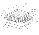
以下、本発明の実施形態を、図面に従って説明する。図1は、本実施形態の超音波振動子ユニット10の完成状態を示す斜視図である。超音波振動子ユニット10は、図1において上方に向けて超音波を送受する。なお、以下の説明において、「上方」や「下面」などの上下の関係を示す語句は、図における上下を示すのに限定したものであり、使用態様等における上下関係を示すものではない。超音波振動子ユニット10は、個振動子12が縦横に配置された二次元のアレイ振動子14を含む。図示するアレイ振動子14は、縦横に同数の個振動子12が配列され、全体として略正方形に構成される。また、図においては、説明のために、個振動子12の数を5×5配置の25個としているが、実際のアレイ振動子14は、格段に多くの、例えば数千個の個振動子12を備えている。この構成においては、超音波ビームを交差する2方向に走査することができる。2方向の走査によって取り込まれた三次元空間内のデータから、三次元空間を表す三次元超音波画像を形成することができる。このデータから任意の断面における超音波画像を形成することもできる。アレイ振動子は、個振動子12が一列に直線状に配列された一次元アレイであってもよい。また、縦方向と横方向において異なる個数の個振動子12を配列した、略長方形のアレイであってもよい。
Hereinafter, embodiments of the present invention will be described with reference to the drawings. FIG. 1 is a perspective view showing a completed state of the
超音波振動子ユニット10は、アレイ振動子14を駆動する電子回路を備えた回路基板16と、アレイ振動子14を覆って保護する保護層18を有する。このユニット10の場合、回路基板16は、電子回路が形成された電子回路基板20と、この電子回路と個振動子12を接続する配線または回路を有する中継基板22を有する。中継基板22は、電子回路上の端子と個振動子12の接続を切り換える機能を有していてもよい。アレイ振動子14は回路基板16より小さく、回路基板16のアレイ振動子14が接合される面(振動子接合面36)の一部が、アレイ振動子14に覆われずに露出している。
The
個振動子12は、圧電素子24を含む振動素子26と整合層28とを含む。振動素子26は圧電素子24のみで構成されてよく、また圧電素子24と共振層30を組み合わせて構成されてもよい。共振層30は、圧電素子24の背面側、つまり超音波を送受する向きの反対側に配置される。また、共振層30は、圧電素子24より音響インピーダンスが高くされており、ハード背面層を形成し、圧電素子24と共振層30が一体となって超音波の送波および受波を行っている。圧電素子24と共振層30の音響インピーダンスはそれぞれ、例えば30MRayls程度、70〜100MRaylsである。共振層30の材料は、例えばコバルトやジルコニア等とタングステン化合物等の複合体である超硬材と呼ばれるものである。共振層30は、圧電素子24と共振して生体に向けて効率よく超音波を発信するのに役立つ。この場合、圧電素子24は、使用する周波数の超音波の波長λに対し、おおよそ四分の1(λ/4)の厚さに調整されている。
The
整合層28は、圧電素子24から生体へ音響インピーダンスを段階的に減少させ、圧電素子24と生体を音響的に整合させるための層である。整合層28は、1層のみにより構成されてもよいが、音響インピーダンスができるだけ滑らかに減少させるために複数の層を有してもよい。図示する例では、第1整合層28A、第2整合層28Bの2層から構成されている。整合層28の材料は樹脂、例えばエポキシ樹脂が用いられる。
The
個振動子12の保護層18に対向する面には、各個振動子12に共通のグランド電極32が接合されている。整合層28は、導電性を有しており、グランド電極32と振動素子26を電気的に接続している。整合層28は、導電性を持たせるために、カーボン、炭素、グラファイト材または導電性フィラーが混入された樹脂を用いることができる。一方、個振動子12の回路基板16に対向する面には、回路基板16の表面に形成された電極パッド34(図2参照)が接続している。振動素子26が圧電素子24のみにより構成される態様においては電極パッド34が直接接続される。振動素子26が共振層30を含む場合、共振層30が導電性とされて、圧電素子24と電極パッド34が電気的に接続される。
A
次に、超音波振動子ユニット10の製造方法について説明する。図2には、回路基板16が示されている。回路基板16は、低温同時焼成セラミックス(LTCC)製である。低温同時焼成セラミックスは、他のセラミックス材料と比較して熱伝導率が低く、切削時に温度が高くなり、切削工具の変形、破損を生じやすい。したがって、低温同時焼成セラミックスを切削する場合には、切削液を十分に供給し冷却を行うこと、また切削工具の剛性を高めて工具の変形が生じないようにすることが必要となる。
Next, a method for manufacturing the
回路基板16の、アレイ振動子14が後に接合される面36(以下、振動子接合面36と記す。)には、電極パッド34が形成されている。この電極パッド34は、回路基板16内に形成された電子回路と電気的に接続されている。
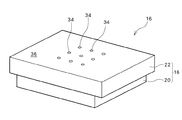
An
図3は、回路基板16の表面に溝が切られた状態を示す図である。回路基板16の振動子接合面36に縦横に溝38を形成する。溝38は、電極パッド34の間を通るように形成される。この溝が図中に符号38aで示されている。溝38はまた、複数の電極パッド34の全体を囲むように形成される。この溝が図中に符号38bで示されている。この結果、溝38で囲まれ、かつ溝38で分割されない一つの区画39に、一つの電極パッド34が配置される。
FIG. 3 is a view showing a state in which a groove is cut on the surface of the
溝38は、切削工具、例えばダイシングソーを用いて加工される。ダイシングソー40の概略構成が図4に示されている。ダイシングソー40は、円環板状のダイシングブレード42(以下、ブレード42と記す。)と、ブレード42を支持するフランジ44を有し、伝達軸46により回転駆動される。後述するように、この実施形態では、回路基板16に溝38を形成するダイシングソーと、個振動子12を形成するダイシングソーとは別のものを使用する。これらを区別するために、前者を符号40Aを用いて、また後者を符号40Bを用いて説明する。ブレード42がフランジ44から突出している量、つまりブレード42とフランジ44の半径の差は刃出し量hと呼ばれている。また、図3に示すように、溝38の幅はw、深さはdである。ブレード42の厚さtをwとすることにより、1回の切削で幅wの溝を形成することができる。溝幅wおよび溝深さdは、例えばそれぞれ0.04〜0.1mm、0.05〜0.3mmとすることができる。
The
溝38は、後述するように、個振動子12を切り出す際のダイシングソー40Bの逃げを作る目的で設けられており、溝深さdは浅くてよい。したがって、回路基板16の、ダイシングソー40Aが切削している部分に切削液を供給することができ、回路基板16およびブレード42が冷却不足にならないようにすることができる。また、ダイシングソー40Aの刃出し量hを小さくすることができ、ブレード42の剛性が高くなり、その変形が抑制される。また、電極パッド34を視認できる状態で溝38の加工を行うことができるので、所定の位置に確実に溝を形成することができる。つまり、電極パッド34を削ってしまわないようにできる。
As will be described later, the
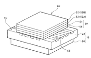
図5は、溝38が形成された回路基板16に振動子ブランク48を接合した状態を示す図である。溝38が切られた後、アレイ振動子14の素材である振動子ブランク48を振動子接合面36に接合する。振動子ブランク48は、後に分割されて振動素子26となる振動素子素材50と、同様に分割されて整合層28となる整合層素材52を含む。振動素子素材50は、圧電素子24となる圧電素子素材54を含む。また、振動素子26が圧電素子24と共振層30を含む場合には、振動素子素材50は共振層30となる共振層素材56を含む。整合層素材52の層数は、整合層28の層数と同じである。各素材は、層をなしており、積層して振動子ブランク48を形成した後、回路基板16上に接合される。また、回路基板16上で順次積層されてもよい。
FIG. 5 is a view showing a state in which the vibrator blank 48 is bonded to the
各層を構成する素材は、隣接する素材に対向する面の全体に電極層を有してよい。電極層は、金、銀、その他の導電性が良好な金属で形成される。電極層形成の手法は、メッキ、蒸着、イオンプレーティング、スパッタリング、焼き付け、化学気相堆積法(CVD)などを採用することができる。また、振動子ブランク48の回路基板16に対向する面、すなわち振動素子素材50の下面の全体に、前記の電極層と同様の電極層を設けることができる。同様に、振動子ブランク48の保護層18に対向する面の全体に前記の電極層と同様の電極層を設けることができる。
The material constituting each layer may have an electrode layer over the entire surface facing the adjacent material. The electrode layer is made of gold, silver, or other metal having good conductivity. As a method for forming the electrode layer, plating, vapor deposition, ion plating, sputtering, baking, chemical vapor deposition (CVD), or the like can be employed. Further, an electrode layer similar to the above electrode layer can be provided on the surface of the vibrator blank 48 facing the
回路基板16と振動子ブランク48の接合は、非導電性の接着剤を用いて行われる。接着剤は、例えばエポキシ系接着剤、ウレタン系接着剤、シアノアクリレート系接着剤などを用いることができる。回路基板16と振動子ブランク48を接着する際、溝38を接着剤により埋めることができる。溝38内に充填された接着剤は、溝38以外の部分に比べて厚いため、回路基板16と振動子ブランク48を強固に接合するのに貢献している。
The
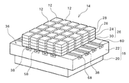
図6は、振動子ブランク48を切断して分割し、個振動子12を形成した状態を示す図である。振動子ブランク48は、回路基板16の表面上にすでに形成されている溝38の位置で切削工具、例えばダイシングソー40Bにより切断される。切断により、振動素子26と整合層28が積層された個振動子12が切り出される。一つの区画39に対して1個の個振動子12を形成してよく、この場合、1個の個振動子12は、1個の電極パッド34に接続される。振動子ブランク48を切断する際に、溝38が視認できるので、溝38の位置に合わせて切断をすることができる。このように、振動子ブランク48を個別の個振動子12に分離してアレイ振動子14が形成されるように、溝38の位置において振動子ブランク48が切断される。振動子ブランク48を溝38の位置で、または溝38に沿って切断することで、電極パッド34の位置に対応して個振動子12を形成することができる。溝38がなければ、振動子ブランク48を切断する際に、目標がなく、溝38がある場合に比べて、加工の確実性が低下する。
FIG. 6 is a diagram showing a state in which the vibrator blank 48 is cut and divided to form
振動子ブランク48の切断は、振動子ブランク48の厚さより深く実施される。つまり、この切断の深さは、振動子ブランク48の厚さにある量αを加えたものである。αは、個振動子12同士を確実に分離することができる値であって、溝38の深さdより小さな値である。例えば、溝38の深さdが0.15mmであれば、αは0.12mmとすることができる。振動子ブランク48の厚さより深く切断することで、溝38を埋めている接着剤58に再び溝が形成される。この溝を再形成溝60と記す。また、振動子ブランク48の、回路基板16に対向する面に電極層が形成されている場合、振動子ブランク48の厚さより深く切断することで、この電極層を確実に切断することができる。一方で、振動子ブランク48の厚さのため、振動子ブランク48の切断の際、深い位置に切削液を供給しにくく、またダイシングソー40Bの刃出し量hを大きくする必要がある。これらは、冷却能力の不足およびダイシングソー40Bの剛性低下を招き、切削加工に関して不利な要因である。しかし、ダイシングソー40Bは、切削の難しい材料からなる回路基板16を切断しないので、切削液の供給量が少なくても、必要な冷却を行うことができる。
The cutting of the vibrator blank 48 is performed deeper than the thickness of the
振動子ブランク48に用いられるダイシングソー40Bのブレード厚さtは、溝38の幅より小さくすることができる。溝38の幅wが0.04〜0.1mmであれば、例えば0.02mmとすることができる。説明の順序から、ダイシングソー40Bのブレード厚さtが、溝38の幅から決められるように記載したが、一般的な設計過程においては、隣接する個振動子12の間隔が先に決定される。よって、実際には、まずダイシングソー40Bのブレード42の厚さtが決定され、これに合わせて溝38の幅wが決定される。また、溝38の深さdも、実際には、個振動子12を確実に分離することができるαが先に決定され、これに合わせて溝38の深さが決定される。
The blade thickness t of the dicing saw 40B used for the vibrator blank 48 can be made smaller than the width of the
図7は、図6の縦断面図である。溝38は、溝38の両側に位置する個振動子12の間隔より広く形成され、個振動子12の下方の一部にも存在する。この溝38に面する個振動子12の下面に接着剤58が接している。溝38に面する部分以外の部分でも、個振動子12と回路基板16は接着剤58により接着されているが、この部分に形成された接着剤58の層の厚さは薄い。これに対して、溝38内の接着剤58の層の厚さは厚く、より強く接着することができる。これにより、個振動子12がより強固に回路基板16に接合され、例えば切断時に受けるダイシングソー40Bからの力による剥がれを防止することができる。
FIG. 7 is a longitudinal sectional view of FIG. The
図8は、隣接する個振動子12の間の隙間を目詰めした状態を示す図である。個振動子12の隙間には、目詰め剤62が充填されている。目詰め剤62は、エポキシ系接着剤、ウレタン系接着剤、シリコーン系接着剤などの接着剤を用いることができ、また接着剤にフィラーを混ぜたものを用いることもできる。目詰め剤62は、接着剤58と同じものを用いてもよい。また、再形成溝60内に目詰め剤62を充填してもよい。
FIG. 8 is a diagram illustrating a state in which a gap between adjacent
最後に、アレイ振動子14の上面に複数の個振動子12に共通のグランド電極32を形成し、更に保護層18を形成する。この結果、図1に示す超音波振動子ユニット10が完成する。グランド電極32と保護層18を形成する工程は、前工程である目詰めの工程を同時に行うようにもできる。例えば、アレイ振動子14に対向する面にグランド電極32が形成された保護層18を用意し、これをアレイ振動子14に接着する際、その接着に使用する接着剤を用いて目詰めも行うようにする。
Finally, the
保護層18は、図1に示す平板形状以外の形状であってもよい。例えば、アレイ振動子14の側面全体、または一部を覆う縁を有するキャップ形状とすることができる。また、保護層18の上面を曲面、特に凸面とすることもできる。
The
10 超音波振動子ユニット、12 個振動子、14 アレイ振動子、16 回路基板、20 電子回路基板、22 中継基板、24 圧電素子、26 振動素子、28 整合層、30 共振層、34 電極パッド、36 振動子接合面、38 溝、48 振動子ブランク、50 振動素子素材、52 整合層素材、54 圧電素子素材、56 共振層素材。 10 ultrasonic transducer units, 12 transducers, 14 array transducers, 16 circuit boards, 20 electronic circuit boards, 22 relay boards, 24 piezoelectric elements, 26 vibration elements, 28 matching layers, 30 resonance layers, 34 electrode pads, 36 transducer interface, 38 groove, 48 transducer blank, 50 transducer element material, 52 matching layer material, 54 piezoelectric element material, 56 resonance layer material.
Claims (7)
溝が形成された回路基板表面に、圧電素子素材の層を有する振動子ブランクを接合するステップと、
回路基板表面の溝の位置に合わせて切削工具を用いて振動子ブランクを切断してアレイ振動子を形成するステップと、
を含む、超音波振動子ユニットの製造方法。 A method of manufacturing an ultrasonic transducer unit having an array transducer,
Bonding a vibrator blank having a layer of piezoelectric element material to a circuit board surface on which grooves are formed;
Cutting the vibrator blank using a cutting tool in accordance with the position of the groove on the circuit board surface to form an array vibrator;
A method for manufacturing an ultrasonic transducer unit, comprising:
さらに回路基板の表面に切削により溝を形成するステップを含み、
前記溝を切削する溝切りブレードの厚さは、振動子ブランクを切断する切断ブレードの厚さより厚い、超音波振動子ユニットの製造方法。 It is a manufacturing method of the ultrasonic transducer unit according to claim 1,
And further comprising the step of forming grooves on the surface of the circuit board by cutting,
The method of manufacturing an ultrasonic transducer unit, wherein a thickness of the grooving blade for cutting the groove is thicker than a thickness of the cutting blade for cutting the transducer blank.
回路基板の溝により分けられた区画に対応して設けられた個振動子からなり、溝が形成された回路基板表面に接合されるアレイ振動子と、
を含み、
回路基板に形成された溝の幅が、この溝の両側に設けられた個振動子の間隔よりも広い、
超音波振動子ユニット。 A circuit board with grooves formed on the surface;
An array transducer which is composed of individual transducers provided corresponding to the sections divided by the grooves of the circuit board, and which is bonded to the surface of the circuit board on which the grooves are formed;
Including
The width of the groove formed in the circuit board is wider than the interval between the individual vibrators provided on both sides of the groove,
Ultrasonic transducer unit.
Priority Applications (1)
| Application Number | Priority Date | Filing Date | Title |
|---|---|---|---|
| JP2012265239A JP2014110601A (en) | 2012-12-04 | 2012-12-04 | Ultrasonic vibrator unit and process of manufacturing the same |
Applications Claiming Priority (1)
| Application Number | Priority Date | Filing Date | Title |
|---|---|---|---|
| JP2012265239A JP2014110601A (en) | 2012-12-04 | 2012-12-04 | Ultrasonic vibrator unit and process of manufacturing the same |
Publications (2)
| Publication Number | Publication Date |
|---|---|
| JP2014110601A true JP2014110601A (en) | 2014-06-12 |
| JP2014110601A5 JP2014110601A5 (en) | 2015-12-24 |
Family
ID=51030972
Family Applications (1)
| Application Number | Title | Priority Date | Filing Date |
|---|---|---|---|
| JP2012265239A Pending JP2014110601A (en) | 2012-12-04 | 2012-12-04 | Ultrasonic vibrator unit and process of manufacturing the same |
Country Status (1)
| Country | Link |
|---|---|
| JP (1) | JP2014110601A (en) |
Cited By (2)
| Publication number | Priority date | Publication date | Assignee | Title |
|---|---|---|---|---|
| CN109326629A (en) * | 2018-09-17 | 2019-02-12 | 武汉华星光电半导体显示技术有限公司 | The motherboard structure and cutting method of flexible OLED display panel |
| JP2019187526A (en) * | 2018-04-18 | 2019-10-31 | キヤノンメディカルシステムズ株式会社 | Ultrasonic probe and ultrasonic diagnostic apparatus |
Citations (3)
| Publication number | Priority date | Publication date | Assignee | Title |
|---|---|---|---|---|
| JPH04218765A (en) * | 1990-03-26 | 1992-08-10 | Toshiba Corp | Ultrasonic probe |
| JP2005087577A (en) * | 2003-09-19 | 2005-04-07 | Fuji Photo Film Co Ltd | Laminated structure body array, method of manufacturing the same, and method of manufacturing ultrasonic transducer array |
| JP2006211058A (en) * | 2005-01-25 | 2006-08-10 | Matsushita Electric Ind Co Ltd | Ultrasonic probe, ultrasonic diagnostic apparatus, and ultrasonic detector |
-
2012
- 2012-12-04 JP JP2012265239A patent/JP2014110601A/en active Pending
Patent Citations (3)
| Publication number | Priority date | Publication date | Assignee | Title |
|---|---|---|---|---|
| JPH04218765A (en) * | 1990-03-26 | 1992-08-10 | Toshiba Corp | Ultrasonic probe |
| JP2005087577A (en) * | 2003-09-19 | 2005-04-07 | Fuji Photo Film Co Ltd | Laminated structure body array, method of manufacturing the same, and method of manufacturing ultrasonic transducer array |
| JP2006211058A (en) * | 2005-01-25 | 2006-08-10 | Matsushita Electric Ind Co Ltd | Ultrasonic probe, ultrasonic diagnostic apparatus, and ultrasonic detector |
Cited By (5)
| Publication number | Priority date | Publication date | Assignee | Title |
|---|---|---|---|---|
| JP2019187526A (en) * | 2018-04-18 | 2019-10-31 | キヤノンメディカルシステムズ株式会社 | Ultrasonic probe and ultrasonic diagnostic apparatus |
| JP7187165B2 (en) | 2018-04-18 | 2022-12-12 | キヤノンメディカルシステムズ株式会社 | Ultrasonic probe and ultrasonic diagnostic equipment |
| CN109326629A (en) * | 2018-09-17 | 2019-02-12 | 武汉华星光电半导体显示技术有限公司 | The motherboard structure and cutting method of flexible OLED display panel |
| WO2020057054A1 (en) * | 2018-09-17 | 2020-03-26 | 武汉华星光电半导体显示技术有限公司 | Motherboard structure for flexible oled display panel and cutting method |
| CN109326629B (en) * | 2018-09-17 | 2021-02-02 | 武汉华星光电半导体显示技术有限公司 | Motherboard structure of flexible OLED display panel and cutting method |
Similar Documents
| Publication | Publication Date | Title |
|---|---|---|
| US6640634B2 (en) | Ultrasonic probe, method of manufacturing the same and ultrasonic diagnosis apparatus | |
| US10561398B2 (en) | Ultrasound transducer and method for wafer level back face attachment | |
| US6894425B1 (en) | Two-dimensional ultrasound phased array transducer | |
| US8319399B2 (en) | Ultrasound probe | |
| EP1690604B1 (en) | Vibrator array, manufacturing method thereof and ultrasonic probe | |
| JP5643667B2 (en) | Ultrasonic transducer, ultrasonic probe, and method of manufacturing ultrasonic transducer | |
| US8978216B2 (en) | Method for forming an acoustical stack for an ultrasound probe | |
| JP2000166923A (en) | Ultrasonic transducer and its manufacture | |
| CN103518385A (en) | Ultrasound transducer, ultrasound probe, and ultrasound transducer manufacturing method | |
| KR100916029B1 (en) | Ultrasonic probe and its method of manufacturing | |
| JP2009082612A (en) | Ultrasonic probe and piezoelectric transducer | |
| JP4528606B2 (en) | Ultrasonic probe and ultrasonic diagnostic apparatus | |
| JP2014110601A (en) | Ultrasonic vibrator unit and process of manufacturing the same | |
| JP6063289B2 (en) | Method for manufacturing ultrasonic transducer unit | |
| US20230415197A1 (en) | Planar Phased Ultrasound Transducer Array | |
| JP2009038675A (en) | Ultrasonic transducer and ultrasonic probe equipped with same | |
| JP4468599B2 (en) | Ultrasonic probe | |
| JP2015228932A (en) | Ultrasonic probe and manufacturing method of the same | |
| JP2009267688A (en) | Ultrasonic probe, method for manufacturing ultrasonic probe and ultrasonograph | |
| US20190350554A1 (en) | Phased array transducers and wafer scale manufacturing for making the same | |
| KR20160038390A (en) | Ultrasonic transducer and method for fabricating the same | |
| JP2008043529A (en) | Electrode structure of ultrasound probe, ultrasound probe, and substrate of ultrasound probe | |
| JP5377742B2 (en) | Ultrasonic probe and ultrasonic transducer | |
| JP5268421B2 (en) | Ultrasonic transducer manufacturing method and ultrasonic probe manufacturing method | |
| JP4071084B2 (en) | Manufacturing method of two-dimensional array ultrasonic probe |
Legal Events
| Date | Code | Title | Description |
|---|---|---|---|
| A521 | Request for written amendment filed |
Free format text: JAPANESE INTERMEDIATE CODE: A523 Effective date: 20151102 |
|
| A621 | Written request for application examination |
Free format text: JAPANESE INTERMEDIATE CODE: A621 Effective date: 20151102 |
|
| A711 | Notification of change in applicant |
Free format text: JAPANESE INTERMEDIATE CODE: A712 Effective date: 20160523 |
|
| A977 | Report on retrieval |
Free format text: JAPANESE INTERMEDIATE CODE: A971007 Effective date: 20160912 |
|
| A131 | Notification of reasons for refusal |
Free format text: JAPANESE INTERMEDIATE CODE: A131 Effective date: 20160920 |
|
| A521 | Request for written amendment filed |
Free format text: JAPANESE INTERMEDIATE CODE: A523 Effective date: 20161116 |
|
| A131 | Notification of reasons for refusal |
Free format text: JAPANESE INTERMEDIATE CODE: A131 Effective date: 20170411 |
|
| A02 | Decision of refusal |
Free format text: JAPANESE INTERMEDIATE CODE: A02 Effective date: 20171010 |