JP2014033185A - Light emitting element and light emitting element package - Google Patents
Light emitting element and light emitting element package Download PDFInfo
- Publication number
- JP2014033185A JP2014033185A JP2013090217A JP2013090217A JP2014033185A JP 2014033185 A JP2014033185 A JP 2014033185A JP 2013090217 A JP2013090217 A JP 2013090217A JP 2013090217 A JP2013090217 A JP 2013090217A JP 2014033185 A JP2014033185 A JP 2014033185A
- Authority
- JP
- Japan
- Prior art keywords
- layer
- light emitting
- layers
- barrier
- disposed
- Prior art date
- Legal status (The legal status is an assumption and is not a legal conclusion. Google has not performed a legal analysis and makes no representation as to the accuracy of the status listed.)
- Pending
Links
- 230000004888 barrier function Effects 0.000 claims abstract description 165
- 239000004065 semiconductor Substances 0.000 claims abstract description 92
- 239000000463 material Substances 0.000 claims description 14
- 150000001875 compounds Chemical class 0.000 claims description 8
- 238000009877 rendering Methods 0.000 abstract description 10
- 239000010410 layer Substances 0.000 description 509
- 238000010586 diagram Methods 0.000 description 24
- 239000000758 substrate Substances 0.000 description 20
- 230000007423 decrease Effects 0.000 description 12
- PXHVJJICTQNCMI-UHFFFAOYSA-N nickel Substances [Ni] PXHVJJICTQNCMI-UHFFFAOYSA-N 0.000 description 12
- 239000010931 gold Substances 0.000 description 9
- 238000005452 bending Methods 0.000 description 8
- 230000000903 blocking effect Effects 0.000 description 8
- 229910052759 nickel Inorganic materials 0.000 description 8
- 239000002019 doping agent Substances 0.000 description 7
- BASFCYQUMIYNBI-UHFFFAOYSA-N platinum Substances [Pt] BASFCYQUMIYNBI-UHFFFAOYSA-N 0.000 description 7
- 239000011651 chromium Substances 0.000 description 6
- 229910052737 gold Inorganic materials 0.000 description 6
- VRIVJOXICYMTAG-IYEMJOQQSA-L iron(ii) gluconate Chemical compound [Fe+2].OC[C@@H](O)[C@@H](O)[C@H](O)[C@@H](O)C([O-])=O.OC[C@@H](O)[C@@H](O)[C@H](O)[C@@H](O)C([O-])=O VRIVJOXICYMTAG-IYEMJOQQSA-L 0.000 description 6
- 239000011241 protective layer Substances 0.000 description 6
- 239000010936 titanium Substances 0.000 description 6
- 229910052804 chromium Inorganic materials 0.000 description 5
- 239000010949 copper Substances 0.000 description 5
- 229910052697 platinum Inorganic materials 0.000 description 5
- 229910052719 titanium Inorganic materials 0.000 description 5
- 229910018072 Al 2 O 3 Inorganic materials 0.000 description 4
- 229910002704 AlGaN Inorganic materials 0.000 description 4
- 229910019897 RuOx Inorganic materials 0.000 description 4
- 229910004298 SiO 2 Inorganic materials 0.000 description 4
- 229910052782 aluminium Inorganic materials 0.000 description 4
- 229910052802 copper Inorganic materials 0.000 description 4
- OAICVXFJPJFONN-UHFFFAOYSA-N Phosphorus Chemical compound [P] OAICVXFJPJFONN-UHFFFAOYSA-N 0.000 description 3
- 238000000605 extraction Methods 0.000 description 3
- 229910052750 molybdenum Inorganic materials 0.000 description 3
- 238000000465 moulding Methods 0.000 description 3
- 230000003287 optical effect Effects 0.000 description 3
- 229910052710 silicon Inorganic materials 0.000 description 3
- 229910052709 silver Inorganic materials 0.000 description 3
- 229910052725 zinc Inorganic materials 0.000 description 3
- 229910018229 Al—Ga Inorganic materials 0.000 description 2
- -1 InGaN Inorganic materials 0.000 description 2
- 239000000969 carrier Substances 0.000 description 2
- 239000004020 conductor Substances 0.000 description 2
- SBYXRAKIOMOBFF-UHFFFAOYSA-N copper tungsten Chemical compound [Cu].[W] SBYXRAKIOMOBFF-UHFFFAOYSA-N 0.000 description 2
- 229910052735 hafnium Inorganic materials 0.000 description 2
- 239000011810 insulating material Substances 0.000 description 2
- 229910052741 iridium Inorganic materials 0.000 description 2
- 229910052763 palladium Inorganic materials 0.000 description 2
- 230000002040 relaxant effect Effects 0.000 description 2
- 229910052718 tin Inorganic materials 0.000 description 2
- 239000011701 zinc Substances 0.000 description 2
- VYZAMTAEIAYCRO-UHFFFAOYSA-N Chromium Chemical compound [Cr] VYZAMTAEIAYCRO-UHFFFAOYSA-N 0.000 description 1
- RYGMFSIKBFXOCR-UHFFFAOYSA-N Copper Chemical compound [Cu] RYGMFSIKBFXOCR-UHFFFAOYSA-N 0.000 description 1
- 229910001218 Gallium arsenide Inorganic materials 0.000 description 1
- ZOKXTWBITQBERF-UHFFFAOYSA-N Molybdenum Chemical compound [Mo] ZOKXTWBITQBERF-UHFFFAOYSA-N 0.000 description 1
- 229910010413 TiO 2 Inorganic materials 0.000 description 1
- 229910003087 TiOx Inorganic materials 0.000 description 1
- RTAQQCXQSZGOHL-UHFFFAOYSA-N Titanium Chemical compound [Ti] RTAQQCXQSZGOHL-UHFFFAOYSA-N 0.000 description 1
- 239000000853 adhesive Substances 0.000 description 1
- 230000001070 adhesive effect Effects 0.000 description 1
- XAGFODPZIPBFFR-UHFFFAOYSA-N aluminium Chemical compound [Al] XAGFODPZIPBFFR-UHFFFAOYSA-N 0.000 description 1
- 229910052788 barium Inorganic materials 0.000 description 1
- 229910052797 bismuth Inorganic materials 0.000 description 1
- 229910052791 calcium Inorganic materials 0.000 description 1
- 230000007547 defect Effects 0.000 description 1
- 239000003989 dielectric material Substances 0.000 description 1
- 238000010292 electrical insulation Methods 0.000 description 1
- 230000007613 environmental effect Effects 0.000 description 1
- 229910052733 gallium Inorganic materials 0.000 description 1
- 229910052732 germanium Inorganic materials 0.000 description 1
- PCHJSUWPFVWCPO-UHFFFAOYSA-N gold Chemical compound [Au] PCHJSUWPFVWCPO-UHFFFAOYSA-N 0.000 description 1
- 229910052738 indium Inorganic materials 0.000 description 1
- 239000004973 liquid crystal related substance Substances 0.000 description 1
- 229910052749 magnesium Inorganic materials 0.000 description 1
- 238000004519 manufacturing process Methods 0.000 description 1
- 239000007769 metal material Substances 0.000 description 1
- 239000011733 molybdenum Substances 0.000 description 1
- 229910052758 niobium Inorganic materials 0.000 description 1
- 239000010955 niobium Substances 0.000 description 1
- TWNQGVIAIRXVLR-UHFFFAOYSA-N oxo(oxoalumanyloxy)alumane Chemical compound O=[Al]O[Al]=O TWNQGVIAIRXVLR-UHFFFAOYSA-N 0.000 description 1
- 230000002093 peripheral effect Effects 0.000 description 1
- 239000000047 product Substances 0.000 description 1
- 239000002096 quantum dot Substances 0.000 description 1
- 239000002210 silicon-based material Substances 0.000 description 1
- 229910052712 strontium Inorganic materials 0.000 description 1
- 239000013589 supplement Substances 0.000 description 1
- 229920003002 synthetic resin Polymers 0.000 description 1
- 239000000057 synthetic resin Substances 0.000 description 1
- 229910052715 tantalum Inorganic materials 0.000 description 1
- 239000011135 tin Substances 0.000 description 1
- HLLICFJUWSZHRJ-UHFFFAOYSA-N tioxidazole Chemical compound CCCOC1=CC=C2N=C(NC(=O)OC)SC2=C1 HLLICFJUWSZHRJ-UHFFFAOYSA-N 0.000 description 1
- 239000012780 transparent material Substances 0.000 description 1
- 229910052721 tungsten Inorganic materials 0.000 description 1
- WFKWXMTUELFFGS-UHFFFAOYSA-N tungsten Chemical compound [W] WFKWXMTUELFFGS-UHFFFAOYSA-N 0.000 description 1
- 239000010937 tungsten Substances 0.000 description 1
Images


Classifications
-
- H—ELECTRICITY
- H01—ELECTRIC ELEMENTS
- H01L—SEMICONDUCTOR DEVICES NOT COVERED BY CLASS H10
- H01L33/00—Semiconductor devices having potential barriers specially adapted for light emission; Processes or apparatus specially adapted for the manufacture or treatment thereof or of parts thereof; Details thereof
- H01L33/02—Semiconductor devices having potential barriers specially adapted for light emission; Processes or apparatus specially adapted for the manufacture or treatment thereof or of parts thereof; Details thereof characterised by the semiconductor bodies
- H01L33/04—Semiconductor devices having potential barriers specially adapted for light emission; Processes or apparatus specially adapted for the manufacture or treatment thereof or of parts thereof; Details thereof characterised by the semiconductor bodies with a quantum effect structure or superlattice, e.g. tunnel junction
-
- H—ELECTRICITY
- H01—ELECTRIC ELEMENTS
- H01L—SEMICONDUCTOR DEVICES NOT COVERED BY CLASS H10
- H01L33/00—Semiconductor devices having potential barriers specially adapted for light emission; Processes or apparatus specially adapted for the manufacture or treatment thereof or of parts thereof; Details thereof
- H01L33/02—Semiconductor devices having potential barriers specially adapted for light emission; Processes or apparatus specially adapted for the manufacture or treatment thereof or of parts thereof; Details thereof characterised by the semiconductor bodies
- H01L33/14—Semiconductor devices having potential barriers specially adapted for light emission; Processes or apparatus specially adapted for the manufacture or treatment thereof or of parts thereof; Details thereof characterised by the semiconductor bodies with a carrier transport control structure, e.g. highly-doped semiconductor layer or current-blocking structure
-
- H—ELECTRICITY
- H01—ELECTRIC ELEMENTS
- H01L—SEMICONDUCTOR DEVICES NOT COVERED BY CLASS H10
- H01L33/00—Semiconductor devices having potential barriers specially adapted for light emission; Processes or apparatus specially adapted for the manufacture or treatment thereof or of parts thereof; Details thereof
- H01L33/02—Semiconductor devices having potential barriers specially adapted for light emission; Processes or apparatus specially adapted for the manufacture or treatment thereof or of parts thereof; Details thereof characterised by the semiconductor bodies
- H01L33/04—Semiconductor devices having potential barriers specially adapted for light emission; Processes or apparatus specially adapted for the manufacture or treatment thereof or of parts thereof; Details thereof characterised by the semiconductor bodies with a quantum effect structure or superlattice, e.g. tunnel junction
- H01L33/06—Semiconductor devices having potential barriers specially adapted for light emission; Processes or apparatus specially adapted for the manufacture or treatment thereof or of parts thereof; Details thereof characterised by the semiconductor bodies with a quantum effect structure or superlattice, e.g. tunnel junction within the light emitting region, e.g. quantum confinement structure or tunnel barrier
Landscapes
- Engineering & Computer Science (AREA)
- Manufacturing & Machinery (AREA)
- Computer Hardware Design (AREA)
- Microelectronics & Electronic Packaging (AREA)
- Power Engineering (AREA)
- Led Devices (AREA)
- Semiconductor Lasers (AREA)
Abstract
Description
本発明は、発光素子に関するものである。 The present invention relates to a light emitting element.
本発明は、発光素子パッケージに関する。 The present invention relates to a light emitting device package.
発光ダイオード(Light-Emitting Diode:LED)は、電流を光に変換させる半導体発光素子(semiconductor light emitting device)である。 A light-emitting diode (LED) is a semiconductor light emitting device that converts current into light.
発光素子は、蛍光灯、白熱灯などのような既存の光源に比べて、低消費電力、半永久的な寿命、速い応答速度、安全性、環境親和性の長所を有する。これによって、既存の光源を半導体発光素子に取り替えるための多くの研究が進められている。 The light emitting device has advantages of low power consumption, semi-permanent lifetime, fast response speed, safety, and environmental compatibility compared to existing light sources such as fluorescent lamps and incandescent lamps. Accordingly, much research has been conducted to replace an existing light source with a semiconductor light emitting device.
併せて、半導体発光素子は室内外で使われる各種ランプ若しくは街灯のような照明装置の光源または液晶表示装置と電光板のような表示装置の光源として広く応用されている。 In addition, semiconductor light-emitting elements are widely applied as light sources for lighting devices such as various lamps or street lamps used indoors and outdoors, or as light sources for display devices such as liquid crystal display devices and lightning plates.
本発明の目的は、演色指数(CRI:Color Rendering Index)を向上させることができる発光素子を提供する。 An object of the present invention is to provide a light emitting device capable of improving a color rendering index (CRI).
本発明の他の目的は、光出力を向上させることができる発光素子を提供することにある。 Another object of the present invention is to provide a light emitting device capable of improving light output.
本発明の更に他の目的は、駆動電圧を低めることができる発光素子を提供することにある。 Still another object of the present invention is to provide a light emitting device capable of lowering a driving voltage.
本発明の様々な実施形態によれば、発光素子は、第1導電型半導体層、前記前記第1導電型半導体層の上に配置された活性層、及び前記前記活性層の上に配置された第2導電型半導体層を含み、前記前記活性層は、(T+1)個のバリア層、前記前記(T+1)個のバリア層の間に配置されたT個の井戸層、及び前記前記第2導電型半導体層に隣り合う(adjacent)N個の井戸層と前記前記N個の井戸層に隣り合うN個のバリア層との間に配置されるダミー層を含み、T>N≧1である。 According to various embodiments of the present invention, a light emitting device is disposed on a first conductive semiconductor layer, an active layer disposed on the first conductive semiconductor layer, and the active layer. The active layer includes (T + 1) barrier layers, T well layers disposed between the (T + 1) barrier layers, and the second conductive layer. Including a dummy layer disposed between N well layers adjacent to the n-type semiconductor layer and N barrier layers adjacent to the N well layers, and T> N ≧ 1.
本発明の様々な実施形態によれば、発光素子は、基板、前記前記基板の上に配置された第1導電型半導体層、前記前記第1導電型半導体層の上に配置された活性層、及び前記前記活性層の上に配置された第2導電型半導体層を含み、前記前記活性層は、第1乃至第4バリア層、及び前記前記第1乃至第4バリア層の間に配置された第1乃至第3井戸層を含み、前記前記第1バリア層は前記前記第1導電型半導体層に接し(contact)、前記前記第4バリア層は前記前記第2導電型半導体層に接し(contact)、前記前記第3及び第4バリア層の厚さは前記前記第1及び第2バリア層の厚さより大きい。 According to various embodiments of the present invention, a light emitting device includes a substrate, a first conductive semiconductor layer disposed on the substrate, an active layer disposed on the first conductive semiconductor layer, And a second conductivity type semiconductor layer disposed on the active layer, wherein the active layer is disposed between the first to fourth barrier layers and the first to fourth barrier layers. The first barrier layer is in contact with the first conductive semiconductor layer, and the fourth barrier layer is in contact with the second conductive semiconductor layer. ), The thicknesses of the third and fourth barrier layers are larger than the thicknesses of the first and second barrier layers.
本発明の様々な実施形態によれば、発光素子パッケージは、支持体、前記前記支持体の上に第1及び第2電極ライン、及び前記前記支持体及び前記前記第1及び第2電極ラインのうち、いずれか1つの上に配置される発光素子を含み、前記前記発光素子は、第1導電型半導体層、前記前記第1導電型半導体層の上に配置された活性層、及び前記前記活性層の上に配置された第2導電型半導体層を含み、前記前記活性層は、(T+1)個のバリア層、前記前記(T+1)個のバリア層の間に配置されたT個の井戸層、及び前記前記第2導電型半導体層に隣り合う(adjacent)N個の井戸層と前記前記N個の井戸層に隣り合うN個のバリア層の間に配置されるダミー層を含み、T>N≧1である。 According to various embodiments of the present invention, the light emitting device package includes a support, first and second electrode lines on the support, and the support and the first and second electrode lines. A light emitting device disposed on any one of the light emitting devices, wherein the light emitting device includes a first conductive semiconductor layer, an active layer disposed on the first conductive semiconductor layer, and the active device. The active layer includes (T + 1) barrier layers and T well layers disposed between the (T + 1) barrier layers. And a dummy layer disposed between N well layers adjacent to the second conductive semiconductor layer and N barrier layers adjacent to the N well layers, and T> N ≧ 1.
本発明を説明するに当たって、各層(膜)、領域、パターン、または構造物が、基板、各層(膜)、領域、パッド、またはパターンの“上(on)”にまたは“下(under)”に形成されるという記載は、直接(directly)または他の層を介して(indirectly)形成されることを全て含む。また、各層の上または下に対する基準は、図面を基準として説明する。 In describing the present invention, each layer (film), region, pattern, or structure is “on” or “under” the substrate, each layer (film), region, pad, or pattern. The description of being formed includes all being formed directly or indirectly through other layers. In addition, the reference to the upper or lower of each layer will be described with reference to the drawings.
以下、添付した図面を参照して実施形態を説明すると、次の通りである。図面において、各層の厚さやサイズは説明の便宜及び明確性のために誇張、省略、または概略的に図示された。また、各構成要素のサイズは実際のサイズを全的に反映するものではない。 Hereinafter, embodiments will be described with reference to the accompanying drawings. In the drawings, the thickness and size of each layer are exaggerated, omitted, or schematically illustrated for convenience of description and clarity. Further, the size of each component does not totally reflect the actual size.
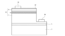
図1は、本発明の実施形態に従う発光素子を示す断面図である。 FIG. 1 is a cross-sectional view illustrating a light emitting device according to an embodiment of the present invention.
図1を参照すると、実施形態に従う発光素子1は、基板3、及び前記前記基板3の上に配置された発光構造物20を含むことができる。
Referring to FIG. 1, the
前記前記基板3は、サファイア(Al2O3)、SiC、Si、GaAs、GaN、ZnO、Si、GaP、InP、及びGeからなるグループから選択された少なくとも1つで形成できる。
The
前記前記基板3と前記前記発光構造物20との間にバッファ層5が配置できるが、これに対して限定するものではない。
A
前記前記バッファ層5は、前記前記基板3と前記前記発光構造物20との間の大きい格子定数(lattice constant)差を緩和してくれるために形成できる。即ち、前記前記基板3の上に前記前記バッファ層5が形成され、前記前記バッファ層5の上に前記前記発光構造物20が形成できる。このような場合、前記前記発光構造物20は前記前記バッファ層5との格子定数の差が小さいので、前記前記発光構造物20が前記前記バッファ層5の上に不良無しで安定的に成長されて電気的及び光学的特性が向上できる。
The
前記前記発光構造物20は、少なくとも第1導電型半導体層7、活性層10、及び第2導電型半導体層9を含むことができるが、これに対して限定するものではない。
The
例えば、前記前記活性層10は前記前記第1導電型半導体層7の上に配置され、前記前記第2導電型半導体層9は前記前記活性層10の上に配置できる。
For example, the
前記前記バッファ層5、前記前記第1導電型半導体層7、前記前記活性層10、及び前記前記第2導電型半導体層9は、II−VI族またはIII−V族化合物半導体材質で形成できる。例えば、前記前記第1導電型半導体層7、前記前記活性層10、及び前記前記第2導電型半導体層9は、InAlGaN、GaN、AlGaN、InGaN、AlN、InN、及びAlInNからなるグループから選択された少なくとも1つを含むことができるが、これに対して限定するものではない。
The
例えば、前記前記第1導電型半導体層7はn型ドーパントを含むn型半導体層であり、前記前記第2導電型半導体層9はp型ドーパントを含むp型半導体層であるが、これに対して限定するものではない。前記前記n型ドーパントは、Si、Ge、Snなどを含み、前記前記p型ドーパントはMg、Zn、Ca、Sr、Baなどを含むが、これに対して限定するものではない。
For example, the first
前記前記活性層10は、前記前記第1導電型半導体層7を通じて注入される第1キャリア、例えば電子と、前記前記第2導電型半導体層9を通じて注入される第2キャリア、例えば正孔とが互いに結合されて、前記前記活性層10の形成物質に従うエネルギーバンドギャップ(energy bandgap)の差に相応する波長を有する光を放出することができる。
The
前記前記活性層10は、単一量子井戸構造(SQW)、多重量子井戸構造(MQW)、量子点構造、または量子線構造のうち、いずれか1つを含むことができる。前記前記活性層10は、井戸層とバリア層とを一周期にして井戸層とバリア層とが繰り返して形成できる。前記前記井戸層とバリア層との反復周期は発光素子の特性によって変形可能であるので、これに対して限定するものではない。
The
前記前記活性層10は、例えば、InGaN/GaNの周期、InGaN/AlGaNの周期、InGaN/InGaNの周期などで形成できる。前記前記バリア層のバンドギャップは、前記前記井戸層のバンドギャップより大きく形成できる。
The
図示してはいないが、前記前記第2導電型半導体層9の上に前記前記第1導電型半導体層7と同一な導電型ドーパントを含む第3導電型半導体層が配置できる。
Although not shown, a third conductive semiconductor layer containing the same conductive dopant as the first
図示してはいないが、前記前記第1導電型半導体層7に接するように第1電極が配置され、前記前記第2導電型半導体層9または前記前記第3導電型半導体層に接するように第2電極が配置できる。
Although not shown, a first electrode is disposed so as to be in contact with the first conductivity
前記前記発光素子1は、水平型(lateral type)構造、フリップチップ型(flip-chip type)構造、及び垂直型(vertical type)構造のうちの1つを含むことができる。
The
前記水平型構造や前記フリップチップ型構造では、前記第1電極は前記第1導電型半導体層7の上に配置され、前記第2電極は前記第2導電型半導体層9の上に配置できる。言い換えると、前記水平型構造や前記フリップチップ型構造では前記第1及び第2電極が同一方向に向けて配置できる。
In the horizontal structure or the flip chip structure, the first electrode may be disposed on the first
前記垂直型構造では、前記第1電極は前記第1導電型半導体層7の上に配置され、前記第2電極は前記第2導電型半導体層9の下に配置できる。言い換えると、前記垂直型構造は前記第1及び第2電極が互いに反対方向に向けて配置され、前記第1及び第2電極の一部が少なくても重畳されるように配置できるが、これに対して限定するものではない。
In the vertical structure, the first electrode may be disposed on the first
図2に示すように、一般的に演色指数(CRI:Color Rendering Index)と光出力とは反比例関係を有することができる。 As shown in FIG. 2, generally, a color rendering index (CRI) and light output can have an inversely proportional relationship.
即ち、発光素子1の波長が増加するほど演色指数は増加することに反して、光出力は減少する。特に、450nm以下のピーク波長では波長が増加するほど演色指数の増加と共に光出力も増加するが、450nmのピーク波長からは波長が増加するほど演色指数は増加するが、光出力は減少する。
That is, the color output increases as the wavelength of the
したがって、450nm以上のピーク波長で演色指数の増加と共に光出力が増加乃至少なくとも維持できる発光素子の開発が切実である。 Therefore, development of a light emitting device capable of increasing or at least maintaining light output with an increase in color rendering index at a peak wavelength of 450 nm or more is eagerly developed.
450nm以上では蛍光体が低下し、蛍光体の低下に起因して光出力が低下する。 When the wavelength is 450 nm or more, the phosphor decreases, and the light output decreases due to the decrease in the phosphor.
発光素子1で450nm以上のピーク波長を有するためには、活性層10のエネルギーバンドギャップの調節が必要である。例えば、活性層10がInGaN井戸層/GaNバリア層の場合、井戸層のIn含有量を調節することによって、エネルギーバンドギャップを調節することができる。ところが、Inの含有量を高めれば、活性層10の膜品質を低下させるので、これを補完するためにバリア層の厚さを増加させる必要がある。バリア層が複数の場合、複数個のバリア層の厚さを全て増加させることによって補完することができる。
In order for the
図3は、活性層10の複数のバリア層の厚さを65Åから70Å、80Å、及び90Åに変化を与えた後、発光素子1の光出力(Po)を測定した実験データである。図3に示すように、バリア層の厚さを増加させればさせるほど、光出力(Po)が低下することが分かる。
FIG. 3 shows experimental data obtained by measuring the light output (Po) of the light-emitting
バリア層の厚さが90Å、80Å、及び70Åに減るほど、450nm以上のピーク波長で光出力は増加することが分かる。即ち、90Åの厚さを有するバリア層よりは80Åの厚さを有するバリア層でより大きい光出力が得られ、80Åの厚さを有するバリア層よりは70Åの厚さのバリア層でより大きい光出力が得られる。但し、90Åの厚さのバリア層、80Åの厚さを有するバリア層、及び70Åの厚さを有するバリア層の全てで波長が増加するにつれて光出力が徐々に減少する傾向を見せている。特に、バリア層の厚さが65Åの場合、光出力が急激に減少する傾向を見せている。 It can be seen that the light output increases at a peak wavelength of 450 nm or more as the thickness of the barrier layer decreases to 90 mm, 80 mm, and 70 mm. That is, a greater light output is obtained with a barrier layer having a thickness of 80 mm than a barrier layer having a thickness of 90 mm, and a greater light output with a barrier layer having a thickness of 70 mm than a barrier layer having a thickness of 80 mm. Output is obtained. However, in all of the barrier layer having a thickness of 90 mm, the barrier layer having a thickness of 80 mm, and the barrier layer having a thickness of 70 mm, the light output tends to gradually decrease as the wavelength increases. In particular, when the thickness of the barrier layer is 65 mm, the light output tends to decrease rapidly.
ここで、活性層に含まれた全てのバリア層の厚さは同一でありうる。例えば、活性層に含まれた全てのバリア層の厚さが90Åでありうる。 Here, the thickness of all the barrier layers included in the active layer may be the same. For example, the thickness of all the barrier layers included in the active layer may be 90 mm.
図3に示すように、バリア層の厚さが減少するにつれて光出力が向上するが、駆動電圧は増加する問題がある。これは、バリア層の厚さが減少するにつれて、活性層のバルク抵抗(bulk resistance)が増加し、このようなバルク抵抗の増加によって駆動電圧が増加することと見える。即ち、バルク抵抗の増加によって電流の流れが妨害を受けるので、所望の電流が流れるためには、より高い駆動電圧が求められる。 As shown in FIG. 3, the light output improves as the thickness of the barrier layer decreases, but there is a problem that the drive voltage increases. It appears that as the barrier layer thickness decreases, the bulk resistance of the active layer increases, and the driving voltage increases with such an increase in bulk resistance. That is, since the current flow is disturbed by an increase in the bulk resistance, a higher drive voltage is required for the desired current to flow.
実施形態は、演色指数及び光出力を向上させながら駆動電圧を低める発光素子を具現することができる。 The embodiment may implement a light emitting device that reduces the driving voltage while improving the color rendering index and the light output.
図4は、図1の発光素子における第1実施形態に従う活性層を示す断面図である。 FIG. 4 is a cross-sectional view showing an active layer according to the first embodiment in the light emitting device of FIG.
図4を参照すると、前記活性層10は、多数のバリア層11a、11b、11c、11d、多数の井戸層13a、13b、13c、及び第1及び第2ダミー層15a、15bを含むことができる。
Referring to FIG. 4, the
前記井戸層13a、13b、13cは、前記バリア層11a、11b、11c、11dの間に配置できる。例えば、第1バリア層11aの上に第1井戸層13aが配置され、前記第1井戸層13aの上に第2バリア層11bが配置され、前記第2バリア層11bの上に第2井戸層13bが配置できる。前記第2井戸層13bの上に第3バリア層11cが配置され、前記第3バリア層11cの上に第3井戸層13cが配置され、前記第3井戸層13cの上に第4バリア層11dが配置できる。
The well layers 13a, 13b, and 13c can be disposed between the barrier layers 11a, 11b, 11c, and 11d. For example, a
前記第1乃至第3井戸層13a、13b、13cは、隣り合うバリア層11a、11b、11c、11dから提供された電子または正孔が詰められることができる。前記電子または正孔が再結合(recombination)して光が生成できる。
The first to third
前記第1ダミー層15aと前記第2ダミー層15bは、前記第3井戸層13cに接して(contact)配置できる。即ち、前記第1ダミー層15aは、前記第4バリア層11dと前記第3井戸層13cに接し(contact)、前記第2ダミー層15bは前記第3井戸層13cと前記第3バリア層11cに接して(contact)配置できるが、これに対して限定するものではない。
The
前記第1及び第2ダミー層15a、15bの各々は、前記第3バリア層11c及び第4バリア層11dに編入できる。これによって、前記第1及び第2ダミー層15a、15bが含まれた前記第3バリア層11c及び第4バリア層11dの各々の厚さが増加して第3井戸層13cと前記第4バリア層11dとの間の格子定数差によるエネルギーバンドが曲がること(band bending)が緩和されて光出力が増加できる。
Each of the first and second dummy layers 15a and 15b can be incorporated into the
これは、450nm以上の主ピーク(main peak)領域を有するように、発光に大きく寄与する第3井戸層13cの化合物半導体材質の組成を調節しても、膜品質には影響を及ぼさない役割をすることができる。
This does not affect the film quality even if the composition of the compound semiconductor material of the
また、第2導電型半導体層9に隣り合う(adjacent)第3バリア層11c及び第4バリア層11dに接して(contact)、第1及び第2ダミー層15a、15bを形成することによって、全体バルク抵抗の増加は最小化しながら光出力を増加させることができる。
Further, the first and second dummy layers 15a and 15b are formed in contact with the
実施形態の活性層10は、450nm以上のピーク波長の光を生成できるが、これに対して限定するものではない。
The
図4には、前記第1及び第2ダミー層15a、15bは第3井戸層13cの両側に配置されることと図示されているが、前記第2ダミー層15bは前記第2導電型半導体層9に隣り合うN個の井戸層と前記N個の井戸層に隣り合うN個のバリア層との間に配置されることもできる。ここで、Nは1以上の自然数(N≧1)である。
FIG. 4 illustrates that the first and second dummy layers 15a and 15b are disposed on both sides of the
この際、全体井戸層はT個であり、全体バリア層は(T+1)個でありうる(T>N)。図示してはいないが、前記第2ダミー層15bは前記第2井戸層13bと前記第3バリア層11cとの間に配置されることもできる。即ち、前記第2バリア層11bの上に前記第2井戸層13bが配置され、前記第2井戸層13bの上に第2ダミー層15bが配置され、前記第2ダミー層15bの上に第3バリア層11cが配置できる。このような場合、前記第2ダミー層15bは前記第3バリア層11cの厚さを増加させて第2井戸層13bと前記第3バリア層11cとの間の格子定数差によるエネルギーバンドが曲がることを緩和して光出力を増加させる役割をすることができる。
At this time, the total number of well layers may be T, and the total number of barrier layers may be (T + 1) (T> N). Although not shown, the
例えば、前記第1乃至第4バリア層11a、11b、11c、11dの各々は、5nmの厚さ(S1、S2、S3、S4)を有し、前記第1及び第2ダミー層15a、15b各々は2nmの厚さ(t1、t2)を有することができるが、これに対して限定するものではない。
For example, each of the first to
前記第1及び第2ダミー層15a、15bの各々は、2nm乃至4nmの範囲の厚さ(t1、t2)を有することができるが、これに対して限定するものではない。2nm以下の厚さは製造することが難しく、4nm以上の厚さの場合、光出力が低下することがある。 Each of the first and second dummy layers 15a and 15b may have a thickness (t1, t2) ranging from 2 nm to 4 nm, but the embodiment is not limited thereto. If the thickness is 2 nm or less, it is difficult to manufacture, and if the thickness is 4 nm or more, the light output may decrease.
図5は、図4の活性層のエネルギーバンドダイヤグラムを示す一例示図である。図5は説明の便宜のために、伝導帯(conduction band)のエネルギーバンドダイヤグラムを図示しているが、エネルギーバンドダイヤグラムは伝導帯及び価電子帯(valance band)を全て含んでいる。 FIG. 5 is an exemplary diagram showing an energy band diagram of the active layer of FIG. For convenience of explanation, FIG. 5 shows an energy band diagram of a conduction band. The energy band diagram includes all of the conduction band and the valence band.
図5に示すように、前記第1乃至第4バリア層11a、11b、11c、11dは同一なエネルギーバンドギャップを有し、前記第1乃至第3井戸層13a、13b、13cより大きいエネルギーバンドギャップを有することができる。したがって、第1乃至第4バリア層11a、11b、11c、11dを経由した電子や正孔が前記第1乃至第3井戸層13a、13b、13cに詰められることができる。
As shown in FIG. 5, the first to
例えば、前記第1乃至第4バリア層11a、11b、11c、11dはGaN、AlGaN、及びInGaNのうちの1つを含むことができ、前記第1乃至第3井戸層13a、13b、13cはInGaNを含むことができるが、これに対して限定するものではない。
For example, the first to
前記第1導電型半導体層7または前記第2導電型半導体層9は、前記第1乃至第4バリア層11a、11b、11c、11dと等しいか大きいバンドギャップを有することができるが、これに対して限定するものではない。例えば、前記第1導電型半導体層7または前記第2導電型半導体層9は、GaNまたはAlGaNを含むことができるが、これに対して限定するものではない。
The first
前記第1及び第2ダミー層15a、15bは、前記第1乃至第4バリア層11a、11b、11c、11dと同一なエネルギーバンドギャップを有することができるが、これに対して限定するものではない。
The first and second dummy layers 15a and 15b may have the same energy band gap as the first to
前記第1及び第2ダミー層15a、15bは、前記第1乃至第4バリア層11a、11b、11c、11dと同一な種類の化合物半導体材質で形成できるが、これに対して限定するものではない。
The first and second dummy layers 15a and 15b may be formed of the same type of compound semiconductor material as the first to
したがって、前記第1及び第2ダミー層15a、15bの各々は、前記第3バリア層11cの厚さ(S3+t1)及び前記第4バリア層11dの厚さ(S4+t2)を実質的に増加させてエネルギーバンドが曲がることを防止する役割をすることができる。
Accordingly, each of the first and second dummy layers 15a and 15b substantially increases the thickness (S3 + t1) of the
前述したように、前記第2ダミー層15bは前記第2井戸層13bと前記第3バリア層11cとの間に配置されることもできるが、これに対して限定するものではない。
As described above, the
前記第2ダミー層15bが前記第2井戸層13bと前記第3バリア層11cとの間に配置されるか、前記第3バリア層11cと前記第3井戸層13cとの間に配置される場合、前記第2ダミー層15bは前記第3バリア層11cの厚さ(S3+t1)を増加させることができる。
When the
図6は、図4の活性層のエネルギーバンドダイヤグラムを示す他の例示図である。図6は説明の便宜のために、伝導帯(conduction band)のエネルギーバンドダイヤグラムを図示しているが、エネルギーバンドダイヤグラムは伝導帯と価電子帯(valance band)を全て含んでいる。 FIG. 6 is another exemplary diagram showing an energy band diagram of the active layer of FIG. For convenience of explanation, FIG. 6 shows an energy band diagram of a conduction band. The energy band diagram includes all of a conduction band and a valence band.
図6に示すように、前記第1乃至第4バリア層11a、11b、11c、11dは互いに同一なエネルギーバンドギャップを有し、前記第1乃至第3井戸層13a、13b、13cより大きいエネルギーバンドギャップを有することができる。
As shown in FIG. 6, the first to
前記第1及び第2ダミー層15a、15bは、前記第1乃至第4バリア層11a、11b、11c、11dと同一な種類の化合物半導体材質で形成できるが、これに対して限定するものではない。
The first and second dummy layers 15a and 15b may be formed of the same type of compound semiconductor material as the first to
前記第1及び第2ダミー層15a、15bは、前記第1乃至第4バリア層11a、11b、11c、11dより小さなエネルギーバンドギャップを有することができるが、これに対して限定するものではない。言い換えると、前記第1及び第2ダミー層15a、15bは、前記第1乃至第3井戸層13a、13b、13cより大きいエネルギーバンドギャップを有し、前記第1乃至第4バリア層11a、11b、11c、11dより小さなエネルギーバンドギャップを有することができるが、これに対して限定するものではない。即ち、前記第1及び第2ダミー層15a、15bは、前記第1乃至第3井戸層13a、13b、13cのバンドギャップと前記第1乃至第4バリア層11a、11b、11c、11dのバンドギャップとの間のバンドギャップを有することができる。
The first and second dummy layers 15a and 15b may have an energy band gap smaller than that of the first to
前記第1及び第2ダミー層15a、15bが前記第1乃至第4バリア層11a、11b、11c、11dより小さいエネルギーバンドギャップを有することによって、電子や正孔がより容易に第3井戸層13cに注入できるので、より多い光を生成して内部量子効率(internal quantum efficiency)が向上できるが、これに対して限定するものではない。
Since the first and second dummy layers 15a and 15b have an energy band gap smaller than those of the first to
前記第1及び第2ダミー層15a、15bの各々は、前記第3バリア層11cの厚さ(S3+t1)及び前記第4バリア層11dの厚さ(S4+t2)を実質的に増加させてエネルギーバンドが曲がることを防止する役割をすることができる。
Each of the first and second dummy layers 15a and 15b substantially increases the thickness (S3 + t1) of the
前述したように、前記第2ダミー層15bは前記第2井戸層13bと前記第3バリア層11cとの間に配置されることもできるが、これに対して限定するものではない。
As described above, the
前記第2ダミー層15bが前記第2井戸層13bと前記第3バリア層11cとの間に配置されるか、前記第3バリア層11cと前記第3井戸層13cとの間に配置される場合、前記第2ダミー層15bは前記第3バリア層11cの厚さ(S3+t1)を増加させることができる。
When the
図7は、図1の発光素子における第2実施形態に従う活性層を示す断面図である。 FIG. 7 is a cross-sectional view showing an active layer according to the second embodiment in the light emitting device of FIG.
図7を参照すると、前記活性層10は、多数のバリア層11a、11b、11c、11d、多数の井戸層13a、13b、13c、及び第1乃至第4ダミー層15a、15b、17a、17bを含むことができる。
Referring to FIG. 7, the
前記3井戸層13a、13b、13cは、前記バリア層11a、11b、11c、11dの間に配置できる。例えば、第1バリア層11aの上に第1井戸層13aが配置され、前記第1井戸層13aの上に第2バリア層11bが配置され、前記第2バリア層11bの上に第2井戸層13bが配置できる。前記第2井戸層13bの上に第3バリア層11cが配置され、前記第3バリア層11cの上に第3井戸層13cが配置され、前記第3井戸層13cの上に第4バリア層11dが配置できる。
The three
前記第1乃至第3井戸層13a、13b、13cは隣り合うバリア層11a、11b、11c、11dから提供された電子または正孔が詰められることができる。前記電子または正孔が再結合して光が生成できる。
The first to third
前記第1ダミー層15a及び前記第2ダミー層15bは、前記第3井戸層13cに接して(contact)配置できる。即ち、前記第1ダミー層13aは前記第4バリア層11dと前記第3井戸層13cに接し(contact)、前記第2ダミー層15bは前記第3井戸層13cと前記第3バリア層11cに接して(contact)配置できるが、これに対して限定するものではない。
The
前記第1及び第2ダミー層15a、15bの各々は、前記第3バリア層11c及び第4バリア層11dの厚さを増加させて第3井戸層13cと前記第4バリア層11dとの間の格子定数差によるエネルギーバンドが曲がること(band bending)を緩和して光出力を増加させる役割をすることができる。
Each of the first and second dummy layers 15a and 15b increases the thickness of the
図示してはいないが、前記第1ダミー層15aは、前記第2井戸層13bと前記第3バリア層11cとの間に配置されることもできる。即ち、前記第2バリア層11cの上に前記第2井戸層13bが配置され、前記第2井戸層13bの上に第2ダミー層15bが配置され、前記第2ダミー層15bの上に第3バリア層11cが配置できる。このような場合、前記第2ダミー層15bは、前記第3バリア層11cの厚さを増加させて第2井戸層13bと前記第3バリア層11cとの間の格子定数差によるエネルギーバンドが曲がることを緩和して光出力を増加させる役割をすることができる。
Although not shown, the
前記第3及び第4ダミー層17a、17bは、前記第1井戸層13aに接して(contact)配置できる。即ち、前記第3ダミー層17aは前記第1バリア層11aと前記第1井戸層13aに接し(contact)、前記第4ダミー層17bは前記第1井戸層13aと前記第2バリア層11bに接して(contact)配置できるが、これに対して限定するものではない。
The third and fourth dummy layers 17a and 17b may be disposed in contact with the
前記第3及び第4ダミー層17a、17bの各々は、前記第1バリア層11a及び第2バリア層11bの厚さを増加させて第1井戸層13aと前記第2バリア層11bとの間の格子定数差によるエネルギーバンドが曲がること(band bending)を緩和して光出力を増加させる役割をすることができる。
Each of the third and fourth dummy layers 17a and 17b increases the thickness of the
前記第3及び第4ダミー層17a、17bは、前記第1乃至第4バリア層11a、11b、11c、11dと同一な種類の化合物半導体材質で形成できるが、これに対して限定するものではない。
The third and fourth dummy layers 17a and 17b may be formed of the same type of compound semiconductor material as the first to
図7には、前記第3及び第4ダミー層17a、17bは第1井戸層13aの両側に配置されることと図示されているが、前記第4ダミー層17bは前記第1導電型半導体層7に隣り合うM個の井戸層と、前記M個の井戸層に隣り合うM個のバリア層との間に配置されることもできる。ここで、Mは1以上の自然数(M≧1)である。
FIG. 7 illustrates that the third and fourth dummy layers 17a and 17b are disposed on both sides of the
併せて、図7には、前記第1及び第2ダミー層15a、15bは第3井戸層13cの両側に配置されることと図示されているが、前記第2ダミー層15bは前記第2導電型半導体層9に隣り合うN個の井戸層と、前記N個の井戸層に隣り合うN個のバリア層との間に配置されることもできる。ここで、Nは1以上の自然数(N≧1)である。
In addition, FIG. 7 illustrates that the first and second dummy layers 15a and 15b are disposed on both sides of the
このような場合、NはMと同一または相異することができる。例えば、NはMより大きいことがあるが、これに対して限定するものではない。 In such a case, N can be the same as or different from M. For example, N may be greater than M, but is not limited thereto.
この際、全体井戸層はT個であり、全体バリア層は(T+1)個でありうる(T>N≧M)。 At this time, the total number of well layers may be T, and the total number of barrier layers may be (T + 1) (T> N ≧ M).
図示してはいないが、前記第4ダミー層17bは前記第2バリア層11bと前記第2井戸層13bとの間に配置されることもできる。即ち、前記第2バリア層11bの上に前記第4ダミー層17bが配置され、前記第4ダミー層17bの上に第2井戸層13bが配置できる。このような場合、前記第4ダミー層17bは前記第2バリア層11bの厚さを増加させて第2井戸層13bと前記第2バリア層11bとの間の格子定数差によるエネルギーバンドが曲がることを緩和して光出力を増加させる役割をすることができる。
Although not shown, the
前記第1及び第2ダミー層15a、15bと前記第3及び第4ダミー層17a、17bとは相異する厚さを有することができる。例えば、前記第1乃至第4バリア層11a、11b、11c、11dの各々は、5nmの厚さ(S1、S2、S3、S4)を有し、前記第1及び第2ダミー層15a、15bの各々は2nmの厚さ(t1、t2)を有し、前記第3及び第4ダミー層17a、17bの各々は1nmの厚さ(u1、u2)を有することができるが、これに対して限定するものではない。
The first and second dummy layers 15a and 15b and the third and fourth dummy layers 17a and 17b may have different thicknesses. For example, each of the first to
例えば、前記第1及び第2ダミー層15a、15bの各々は2nm乃至4nmの範囲の厚さ(t1、t2)を有し、前記第3及び第4ダミー層17a、17bの各々は1nm乃至2nmの範囲の厚さ(u1、u2)を有することができるが、これに対して限定するものではない。 For example, each of the first and second dummy layers 15a and 15b has a thickness (t1, t2) in a range of 2 nm to 4 nm, and each of the third and fourth dummy layers 17a and 17b has a thickness of 1 nm to 2 nm. The thickness (u1, u2) can be, but is not limited thereto.
図8は、図7の活性層のエネルギーバンドダイヤグラムを示す一例示図である。図8は説明の便宜のために、伝導帯(conduction band)のエネルギーバンドダイヤグラムを図示しているが、エネルギーバンドダイヤグラムは伝導帯と価電子帯(valance band)を全て含んでいる。 FIG. 8 is an exemplary diagram showing an energy band diagram of the active layer of FIG. For convenience of explanation, FIG. 8 shows an energy band diagram of a conduction band. The energy band diagram includes all of the conduction band and the valence band.
図8は、第3及び第4ダミー層を除いては図5とほとんど類似または同一であるので、第3及び第4ダミー層を中心として説明する。 Since FIG. 8 is almost similar or identical to FIG. 5 except for the third and fourth dummy layers, the description will focus on the third and fourth dummy layers.
図8に示すように、前記第1乃至第4バリア層11a、11b、11c、11dは同一なエネルギーバンドギャップを有し、前記第1乃至第3井戸層13a、13b、13cより大きいエネルギーバンドギャップを有することができる。
As shown in FIG. 8, the first to
前記第1及び第2ダミー層15a、15bは、前記第1乃至第4バリア層11a、11b、11c、11dと同一なエネルギーバンドギャップを有することができるが、これに対して限定するものではない。
The first and second dummy layers 15a and 15b may have the same energy band gap as the first to
前記第1及び第2ダミー層15a、15bは前記第1乃至第4バリア層と同一な種類の化合物半導体材質で形成できるが、これに対して限定するものではない。 The first and second dummy layers 15a and 15b may be formed of the same type of compound semiconductor material as the first to fourth barrier layers, but the embodiment is not limited thereto.
したがって、前記第1及び第2ダミー層15a、15bの各々は、前記第3バリア層11cの厚さ(S3+t1)及び前記第4バリア層11dの厚さ(S4+t2)を実質的に増加させてエネルギーバンドが曲がることを防止する役割をすることができる。
Accordingly, each of the first and second dummy layers 15a and 15b substantially increases the thickness (S3 + t1) of the
併せて、第3及び第4ダミー層17a、17bは前記第1乃至第4バリア層11a、11b、11c、11dと同一なエネルギーバンドギャップを有することができるが、これに対して限定するものではない。
In addition, the third and fourth dummy layers 17a and 17b may have the same energy band gap as the first to
前記第3及び第4ダミー層17a、17bは、前記第1乃至第4バリア層11a、11b、11c、11dと同一な種類の化合物半導体材質で形成できるが、これに対して限定するものではない。
The third and fourth dummy layers 17a and 17b may be formed of the same type of compound semiconductor material as the first to
したがって、前記第3及び第4ダミー層17a、17bの各々は、前記第1バリア層11aの厚さ(S1+u1)及び前記第2バリア層11bの厚さ(S2+u2)を実質的に増加させてエネルギーバンドが曲がることを防止する役割をすることができる。
Accordingly, each of the third and fourth dummy layers 17a and 17b substantially increases the thickness (S1 + u1) of the
図9は、図7の活性層のエネルギーバンドダイヤグラムを示す他の例示図である。図9は説明の便宜のために、伝導帯(conduction band)のエネルギーバンドダイヤグラムを図示しているが、エネルギーバンドダイヤグラムは伝導帯と価電子帯(valance band)を全て含んでいる。 FIG. 9 is another exemplary diagram showing an energy band diagram of the active layer of FIG. For convenience of explanation, FIG. 9 shows an energy band diagram of a conduction band. The energy band diagram includes all of a conduction band and a valence band.
図8は、第3及び第4ダミー層を除いては図6とほとんど類似または同一であるので、第3及び第4ダミー層を中心として説明する。 Since FIG. 8 is almost similar or identical to FIG. 6 except for the third and fourth dummy layers, the description will focus on the third and fourth dummy layers.
図9に示すように、前記第3及び第4ダミー層17a、17bは、前記第1乃至第4バリア層11a、11b、11c、11dより小さなエネルギーバンドギャップを有することができるが、これに対して限定するものではない。言い換えると、前記第3及び第4ダミー層17a、17bは、前記第1乃至第3井戸層13a、13b、13cより大きいエネルギーバンドギャップを有し、前記第1乃至第4バリア層11a、11b、11c、11dより小さなエネルギーバンドギャップを有することができるが、これに対して限定するものではない。即ち、前記第3及び第4ダミー層17a、17bは、前記第1乃至第3井戸層13a、13b、13cのバンドギャップと前記第1乃至第4バリア層11a、11b、11c、11dのバンドギャップとの間のバンドギャップを有することができる。
As shown in FIG. 9, the third and fourth dummy layers 17a and 17b may have a smaller energy band gap than the first to
前記第3及び第4ダミー層17a、17bの各々は、前記第1バリア層11aの厚さ(S1+u1)及び前記第2バリア層11bの厚さ(S2+u2)を実質的に増加させてエネルギーバンドが曲がることを防止する役割をすることができる。
Each of the third and fourth dummy layers 17a and 17b substantially increases the thickness (S1 + u1) of the
前述したように、前記第4ダミー層17bは前記第2バリア層11bと前記第2井戸層13bとの間に配置されることもできるが、これに対して限定するものではない。
As described above, the
図10は、従来と実施形態の波長に従う光出力を示すグラフである。 FIG. 10 is a graph showing the optical output according to the wavelength of the prior art and the embodiment.
図10に示すように、従来には450nm以下のピーク波長に主に光出力が分布することに反して、第1及び第2実施形態では450nm以上のピーク波長に主に光出力が分布するだけでなく、光出力も従来に比べて増加することが分かる。 As shown in FIG. 10, in contrast to the conventional case where the light output is mainly distributed at the peak wavelength of 450 nm or less, in the first and second embodiments, only the light output is mainly distributed at the peak wavelength of 450 nm or more. In addition, it can be seen that the light output also increases as compared with the prior art.
ここで、第1実施形態は図4の第1実施形態に従う活性層を含む発光素子を意味するものであって、図面のMQB 5577であり、第2実施形態は図7の第2実施形態に従う活性層を含む発光素子を意味するものであって、図面のMQB 667でありうる。
Here, the first embodiment means a light emitting device including an active layer according to the first embodiment of FIG. 4 and is
図11は、従来と実施形態の駆動電圧を示すグラフである。 FIG. 11 is a graph showing the driving voltage of the conventional example and the embodiment.
従来の場合、3.028Vの駆動電圧であることに反して、第1実施形態は3.029Vの駆動電圧であり、第2実施形態は3.008の駆動電圧が使用できる。 In the conventional case, the driving voltage is 3.028V, whereas the driving voltage of 3.029V is used in the first embodiment, and the driving voltage of 3.008 can be used in the second embodiment.
特に、第2実施形態は従来に比べてバリア層の厚さが増加するにもかかわらず、駆動電圧がより低くなることが分かる。 In particular, it can be seen that the driving voltage is lower in the second embodiment, although the thickness of the barrier layer is increased as compared with the conventional embodiment.
図10及び図11から分かるように、実施形態に従う発光素子は450nm以上のピーク波長で演色指数と光出力が向上し、駆動電圧が低くなる。 As can be seen from FIGS. 10 and 11, the light emitting device according to the embodiment has an improved color rendering index and light output at a peak wavelength of 450 nm or more, and a driving voltage is lowered.
以上の実施形態ではダミー層をバリア層と区分して説明したが、ダミー層とバリア層とを1つの層として見なすこともできる。即ち、第1ダミー層15aは第4バリア層11dに含まれて、第4バリア層11dの厚さはS4+t2に定義され、第2ダミー層15bは第3バリア層11cに含まれて、第3バリア層11cの厚さはS3+t1に定義できる。第3ダミー層17aは第1バリア層11aに含まれて、第1バリア層11aの厚さはS1+u1に定義され、第4ダミー層17bは第2バリア層11bに含まれて、第2バリア層11bの厚さはS2+u2に定義できる。
In the above embodiment, the dummy layer is described as being separated from the barrier layer. However, the dummy layer and the barrier layer can be regarded as one layer. That is, the
図12乃至図14は、図1の発光素子が実際に採用された製品を図示する。 12 to 14 illustrate products in which the light emitting device of FIG. 1 is actually employed.
図12は、本発明の実施形態に従う水平型発光素子を示す断面図である。 FIG. 12 is a cross-sectional view illustrating a horizontal light emitting device according to an embodiment of the present invention.
図12を参照すると、実施形態に従う水平型発光素子は、基板3、バッファ層5、発光構造物20、導電層32、及び第1及び第2電極34、36を含むことができる。
Referring to FIG. 12, the horizontal light emitting device according to the embodiment may include a
前記基板3、前記バッファ層5、及び前記発光構造物20は、既に先に詳細に説明したことがあるので、これ以上の説明は省略する。
Since the
前記導電層32は前記発光構造物20、具体的に第2導電型半導体層9の上に配置できる。もし、前記第2導電型半導体層9の上に第1導電型半導体層7と同一な導電型ドーパントを含む第3導電型半導体層が配置される場合、前記導電層32は前記第3導電型半導体層の上に配置できる。
The
前記導電層32は電流をスプレッディングする役割をするか、前記発光構造物20とオーミックコンタクトを形成して前記発光構造物20にさらに容易に電流が流れるようにする役割をすることができるが、これに対して限定するものではない。
The
前記導電層32は、光が透過される透明な導電物質で形成できる。前記透明な導電物質には、ITO、IZO(In−ZnO)、GZO(Ga−ZnO)、AZO(Al−ZnO)、AGZO(Al−Ga ZnO)、IGZO(In−Ga ZnO)、IrOx、RuOx、RuOx/ITO、Ni/IrOx/Au、及びNi/IrOx/Au/ITOからなるグループから選択された少なくとも1つが含まれることができるが、これに対して限定するものではない。
The
前記第1電極34は前記第1導電型半導体層7に電気的に連結され、前記第2電極36は前記導電層32に電気的に連結できるが、これに対して限定するものではない。
The
前記第1及び第2電極34、36は、例えばAl、Ti、Cr、Ni、Pt、Au、W、Cu、及びMoからなるグループから選択された1つまたはこれらの積層を含むことができるが、これに対して限定するものではない。
For example, the first and
図示してはいないが、前記第1及び第2電極34、36の各々の下部に電流が集中することを防止するための電流遮断層が配置できる。
Although not shown, a current blocking layer for preventing current from concentrating below each of the first and
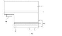
図13は、本発明の実施形態に従うフリップ型発光素子を示す断面図である。 FIG. 13 is a cross-sectional view illustrating a flip-type light emitting device according to an embodiment of the present invention.
図13は、反射層を除いては図12とほとんど類似している。 FIG. 13 is almost similar to FIG. 12 except for the reflective layer.
図13を参照すると、実施形態に従うフリップ型発光素子は、基板3、バッファ層5、発光構造物20、反射層42、及び第1及び第2電極44、46を含むことができる。
Referring to FIG. 13, the flip-type light emitting device according to the embodiment may include a
前記バッファ層5は前記基板3の下に配置され、前記発光構造物20は前記バッファ層5の下に配置され、前記反射層42は前記発光構造物20の下に配置され、前記第1電極44は前記第1導電型半導体層7の下に配置され、前記第2電極46は前記第2導電型半導体層9の下に配置できるが、これに対して限定するものではない。
The
前記基板3、前記バッファ層5、及び前記発光構造物20は、既に先に詳細に説明したことがあるので、これ以上の説明は省略する。
Since the
前記反射層42は前記発光構造物20、具体的に第2導電型半導体層9の上に配置できる。前記第2導電型半導体層9の下に第1導電型半導体層7と同一な導電型ドーパントを含む第3導電型半導体層が配置される場合、前記反射層42は前記第3導電型半導体層の下に配置できる。
The
前記反射層42は活性層10で生成されて下方に進行された光を上方に反射させて発光効率を向上させる役割をすることができるが、これに対して限定するものではない。
The
前記反射層42は反射特性に優れる反射物質を含むが、例えば、Ag、Ni、Al、Rh、Pd、Ir、Ru、Mg、Zn、Pt、Au、及びHfからなるグループから選択された1つまたはこれらの積層を含むことができるが、これに対して限定するものではない。
The
前記反射層42が前記第2導電型半導体層9とのオーミックコンタクト特性がよくない場合、導電層(図示せず)が前記第2導電型半導体層9と前記反射層42との間に配置できるが、これに対して限定するものではない。前記導電層は、前記第2導電型半導体層9とのオーミックコンタクト特性に優れる透明な材質で形成できる。例えば、前記導電層は、ITO、IZO(In−ZnO)、GZO(Ga−ZnO)、AZO(Al−ZnO)、AGZO(Al−Ga ZnO)、IGZO(In−Ga ZnO)、IrOx、RuOx、RuOx/ITO、Ni/IrOx/Au、及びNi/IrOx/Au/ITOからなるグループから選択された少なくとも1つを含むことができるが、これに対して限定するものではない。
If the ohmic contact characteristic between the
図14は、本発明の実施形態に従う垂直型発光素子を示す断面図である。 FIG. 14 is a cross-sectional view illustrating a vertical light emitting device according to an embodiment of the present invention.
図14の説明で、図12に図示された同一な機能を有する構成要素に対しては詳細な説明は省略する。 In the description of FIG. 14, detailed description of components having the same function illustrated in FIG. 12 is omitted.
図14を参照すると、実施形態に従う垂直型発光素子は、支持基板(support substrate)61、接合層(adhesion layer)59、電極層57、オーミックコンタクト層55、電流遮断層(current blocking layer)53、チャンネル層51、保護層(protective layer)63、及び電極65を含むことができる。
Referring to FIG. 14, the vertical light emitting device according to the embodiment includes a
前記支持基板61は、その上に形成される複数の層を支持するだけでなく、電極としての機能を有することができる。
The
前記支持基板61は、例えば、チタン(Ti)、クロム(Cr)、ニッケル(Ni)、アルミニウム(Al)、白金(Pt)、金(Au)、タングステン(W)、銅(Cu)、モリブデン(Mo)、及び銅−タングステン(Cu−W)のうち、少なくとも1つを含むことができる。
The
前記接合層59はボンディング層であって、前記電極層57と前記支持基板61との間に形成される。前記接合層59は電極層57と前記支持基板61との間の接着力を強化させる媒介体の役割をすることができる。
The
前記接合層59は、例えば、Ti、Au、Sn、Ni、Nb、Cr、Ga、In、Bi、Cu、Ag、及びTaからなるグループから選択された少なくとも1つを含むことができる。
For example, the
前記電極層57は活性層10に電源を供給する電極としての役割をし、活性層10から生成されて下方に進行された光を反射させる役割をすることができる。前記電極層57を反射層と命名することもできる。
The
もし、前記電極層57が前記第2導電型半導体層9とオーミックコンタクトに優れる場合、前記オーミックコンタクト層55は省略できる。このような場合、前記電極層57は、電極、反射機能、及びオーミックコンタクト機能を有することができる。
If the
前記電極層57は、例えば、Ag、Ni、Al、Rh、Pd、Ir、Ru、Mg、Zn、Pt、Au、及びHfからなるグループから選択された1つまたはこれらの積層を含むことができるが、これに対して限定するものではない。
The
前記電極層57と前記第2導電型半導体層9の周辺領域の周りに沿ってチャンネル層51が形成できる。前記チャンネル層51は前記オーミックコンタクト層55が省略された場合、前記電極層57と前記第2導電型半導体層9により囲まれるように配置できる。
A
前記チャンネル層51は外部の異質物による電極層57の側面と発光構造物20の側面との間の電気的なショートを防止することができる。
The
前記チャンネル層51は絶縁物質、例えば、SiO2、SiOx、SiOxNy、Si3N4、Al2O3からなるグループから選択された少なくとも1つを含むことができる。
The
電流の集中を防止するために、電流遮断層53が前記第2導電型半導体層9と前記電極層57との間に配置できる。
In order to prevent current concentration, a
前記電流遮断層53は、少なくとも前記電極65の一部領域と重畳するように配置できる。
The
垂直型発光素子では、電極層57は板形状であることに反して、電極65は前記発光構造物20の一部領域のみに形成されるパターン形状であるので、前記電極65と前記電極層57に電源が印加される場合、前記電極65の垂直方向に沿って電流が集中的に流れるようになる。したがって、前記電極65に垂直に重畳される位置に電流遮断層53が配置されることによって、前記電極65に垂直に流れる電流が前記電流遮断層53の周辺に分散される。
In the vertical light emitting device, the
前記電流遮断層53は前記電極層57より小さな電気伝導性を有するか、前記電極層57より大きい電気絶縁性を有するか、前記発光構造物20とショットキー接触を形成する材質を用いて形成できる。前記電流遮断層53は、例えば、ITO、IZO、IZTO、IAZO、IGZO、IGTO、AZO、ATO、ZnO、SiO2、SiOx、SiOxNy、Si3N4、Al2O3、TiOx、Ti、Al、及びCrからなるグループから選択された少なくとも1つを含むことができる。ここで、前記SiO2、SiOx、SiOxNy、Si3N4、Al2O3は絶縁物質でありうる。
The
前記発光構造物20の側面の周りに沿って保護層63が配置できる。前記保護層63は一領域が前記チャンネル層51の上面に接触され、他領域が前記第1導電型半導体層7の上面の周辺領域(peripheral region)に配置できる。
A
前記保護層63は、前記発光構造物20と支持基板61との間の電気的ショートを防止する役割をすることができる。前記保護層63は、例えば、SiO2、SiOx、SiOxNy、Si3N4、TiO2、及びAl2O3からなるグループから選択された1つを含む絶縁性材質を含むことができるが、これに対して限定するものではない。
The
前記保護層63は前記チャンネル層51と同一な物質を含むことができるが、これに対して限定するものではない。
The
前記第1導電型半導体層7の上面には光を効率的に抽出するための光抽出構造が形成できる。前記光抽出構造は、凹凸やラフネス構造を有することができる。前記凹凸は一定に、またはランダムに形成できる。
A light extraction structure for efficiently extracting light may be formed on the upper surface of the first
前記光抽出構造の上に電極65が配置できる。
An
前記電極65は、例えばAl、Ti、Cr、Ni、Pt、Au、W、Cu、及びMoからなるグループから選択された1つまたはこれらの積層を含むことができるが、これに対して限定するものではない。
The
図15は、本発明の実施形態に従う発光素子パッケージを示す断面図である。 FIG. 15 is a cross-sectional view illustrating a light emitting device package according to an embodiment of the present invention.
図15を参照すると、実施形態に従う発光素子パッケージは、支持体101と、前記支持体101に設置された第1電極ライン103及び第2電極ライン105と、前記第1電極ライン103及び第2電極ライン105から電源の供給を受ける発光素子107と、前記発光素子107を囲むモールディング部材113とを含む。
Referring to FIG. 15, the light emitting device package according to the embodiment includes a
前記支持体101は、シリコン材質、合成樹脂材質、または金属材質を含んで形成されることができ、前記発光素子107の周囲に傾斜面が形成できる。
The
前記第1電極ライン103及び第2電極ライン105は互いに電気的に分離され、前記発光素子107に電源を提供する。
The
また、前記第1及び第2電極ライン103、105は、前記発光素子107で発生された光を反射させて光効率を増加させることができ、前記発光素子107で発生された熱を外部に排出させる役割をすることもできる。
In addition, the first and
前記発光素子107は、前記第1電極ライン103、第2電極ライン105、及び前記支持体101のうち、いずれか1つの上に設置されることができ、ワイヤー方式、ダイボンディング方式などにより前記第1及び第2電極ライン103、105に電気的に連結できるが、これに対して限定するものではない。例えば、前記発光素子107の一側、例えば前記発光素子107の背面は前記第1電極ライン103の上面に電気的に接し、前記発光素子107の他側はワイヤー109を用いて前記第2電極ライン105に電気的に連結できる。
The
実施形態の発光素子107は、前述した水平型発光素子、フリップ型発光素子、及び垂直型発光素子のうちのいずれか1つであるが、これに対して限定するものではない。
The
前記モールディング部材113は、前記発光素子107を囲んで前記発光素子107を保護することができる。また、前記モールディング部材113には蛍光体が含まれて前記発光素子107から放出された光の波長を変化させることができる。
The
実施形態に従う発光素子パッケージは、COB(Chip On Board)タイプを含み、前記支持体101の上面は平らで、前記支持体101には複数の発光素子107が設置されることもできる。
The light emitting device package according to the embodiment includes a COB (Chip On Board) type, and the upper surface of the
実施形態は、バリア層に隣接してバリア層と類似するバンドギャップを有するダミー層を形成することによって、450nm以上のピーク波長で演色指数と光出力が向上し、電圧が低くなる。 In the embodiment, by forming a dummy layer having a band gap similar to the barrier layer adjacent to the barrier layer, the color rendering index and the light output are improved at a peak wavelength of 450 nm or more, and the voltage is lowered.
Claims (17)
前記第1導電型半導体層の上に配置された活性層と、
前記活性層の上に配置された第2導電型半導体層と、を含み、
前記活性層は、
(T+1)個のバリア層と、
前記(T+1)個のバリア層の間に配置されたT個の井戸層と、
前記第2導電型半導体層に隣り合う(adjacent)N個の井戸層と前記N個の井戸層に隣り合うN個のバリア層との間に配置される第1ダミー層と、を含み、
T>N≧1であることを特徴とする、発光素子。 A first conductivity type semiconductor layer;
An active layer disposed on the first conductive semiconductor layer;
A second conductivity type semiconductor layer disposed on the active layer,
The active layer is
(T + 1) barrier layers;
T well layers disposed between the (T + 1) barrier layers;
A first dummy layer disposed between N well layers adjacent to the second conductivity type semiconductor layer and N barrier layers adjacent to the N well layers;
T> N ≧ 1, wherein the light emitting element.
前記第1導電型半導体層に隣り合うM個の井戸層と前記M個の井戸層に隣り合うM個のバリア層との間に配置される第2ダミー層をさらに含み、
N≧M≧1であることを特徴とする、請求項1に記載の発光素子。 The active layer is
A second dummy layer disposed between the M well layers adjacent to the first conductivity type semiconductor layer and the M barrier layers adjacent to the M well layers;
The light emitting device according to claim 1, wherein N ≧ M ≧ 1.
前記第2導電型半導体層に接する(contact)第1バリア層と前記第1バリア層に接する第1井戸層との間に配置される第3ダミー層をさらに含むことを特徴とする、請求項1乃至4のうち、いずれか1項に記載の発光素子。 The active layer is
The semiconductor device may further include a third dummy layer disposed between a first barrier layer in contact with the second conductive semiconductor layer and a first well layer in contact with the first barrier layer. 5. The light emitting element according to any one of 1 to 4.
前記第1導電型半導体層に接する第3バリア層と前記第3バリア層に接する第2井戸層との間に配置される第4ダミー層をさらに含むことを特徴とする、請求項1乃至7のうち、いずれか1項に記載の発光素子。 The active layer is
8. The method according to claim 1, further comprising a fourth dummy layer disposed between a third barrier layer in contact with the first conductivity type semiconductor layer and a second well layer in contact with the third barrier layer. The light emitting element of any one of these.
前記第2導電型半導体層はp型半導体層であることを特徴とする、請求項1乃至15のうち、いずれか1項に記載の発光素子。 The first conductive semiconductor layer is an n-type semiconductor layer;
The light emitting device according to claim 1, wherein the second conductive semiconductor layer is a p-type semiconductor layer.
前記支持体の上に第1及び第2電極ラインと、
前記支持体及び前記第1及び第2電極ラインのうちのいずれか1つの上に配置され、請求項1乃至16のうち、いずれか1項による発光素子と、
を含むことを特徴とする、発光素子パッケージ。 A support;
First and second electrode lines on the support;
The light emitting device according to any one of claims 1 to 16, wherein the light emitting device is disposed on any one of the support and the first and second electrode lines.
A light emitting device package comprising:
Applications Claiming Priority (2)
| Application Number | Priority Date | Filing Date | Title |
|---|---|---|---|
| KR1020120086010A KR20140019635A (en) | 2012-08-06 | 2012-08-06 | Light emitting device and light emitting device package |
| KR10-2012-0086010 | 2012-08-06 |
Publications (2)
| Publication Number | Publication Date |
|---|---|
| JP2014033185A true JP2014033185A (en) | 2014-02-20 |
| JP2014033185A5 JP2014033185A5 (en) | 2016-06-16 |
Family
ID=50024575
Family Applications (1)
| Application Number | Title | Priority Date | Filing Date |
|---|---|---|---|
| JP2013090217A Pending JP2014033185A (en) | 2012-08-06 | 2013-04-23 | Light emitting element and light emitting element package |
Country Status (3)
| Country | Link |
|---|---|
| US (1) | US9349914B2 (en) |
| JP (1) | JP2014033185A (en) |
| KR (1) | KR20140019635A (en) |
Families Citing this family (7)
| Publication number | Priority date | Publication date | Assignee | Title |
|---|---|---|---|---|
| JP2015018840A (en) * | 2013-07-08 | 2015-01-29 | 株式会社東芝 | Semiconductor light-emitting element |
| US9640716B2 (en) * | 2015-07-28 | 2017-05-02 | Genesis Photonics Inc. | Multiple quantum well structure and method for manufacturing the same |
| WO2017062451A1 (en) | 2015-10-05 | 2017-04-13 | Precision Biosciences, Inc. | Genetically-modified cells comprising a modified human t cell receptor alpha constant region gene |
| EP3940070A1 (en) | 2015-10-05 | 2022-01-19 | Precision Biosciences, Inc. | Engineered meganucleases with recognition sequences found in the human t cell receptor alpha constant region gene |
| WO2018073393A2 (en) | 2016-10-19 | 2018-04-26 | Cellectis | Tal-effector nuclease (talen) -modified allogenic cells suitable for therapy |
| EP3645038A1 (en) | 2017-06-30 | 2020-05-06 | Precision Biosciences, Inc. | Genetically-modified t cells comprising a modified intron in the t cell receptor alpha gene |
| CA3095795A1 (en) | 2018-04-12 | 2019-10-17 | Precision Biosciences, Inc. | Optimized engineered nucleases having specificity for the human t cell receptor alpha constant region gene |
Citations (15)
| Publication number | Priority date | Publication date | Assignee | Title |
|---|---|---|---|---|
| JPH10242512A (en) * | 1997-02-24 | 1998-09-11 | Toshiba Corp | Semiconductor light emitting device |
| JP2000082676A (en) * | 1998-06-26 | 2000-03-21 | Sharp Corp | Crystal growth method of nitride compound semiconductor, light-emitting device, and its manufacture |
| JP2002344020A (en) * | 2001-05-15 | 2002-11-29 | Sharp Corp | Nitride-based semiconductor light-emitting device |
| JP2003037291A (en) * | 2001-07-25 | 2003-02-07 | Nichia Chem Ind Ltd | Light-emitting element |
| JP2003046200A (en) * | 2001-07-31 | 2003-02-14 | Anritsu Corp | Multiple quantum well semiconductor element |
| JP2003234545A (en) * | 2002-02-07 | 2003-08-22 | Sanyo Electric Co Ltd | Semiconductor light emitting element |
| JP2003535453A (en) * | 1998-11-16 | 2003-11-25 | エムコア・コーポレイション | Group III nitride quantum well structure having indium-rich cluster and method of manufacturing the same |
| JP2004022989A (en) * | 2002-06-19 | 2004-01-22 | Sharp Corp | Nitride semiconductor laser and manufacturing method thereof |
| JP2004031770A (en) * | 2002-06-27 | 2004-01-29 | Sharp Corp | Nitride semiconductor light emitting device |
| JP2004112000A (en) * | 2004-01-13 | 2004-04-08 | Toshiba Corp | Method for manufacturing semiconductor light emitting device |
| JP2004356256A (en) * | 2003-05-28 | 2004-12-16 | Sharp Corp | Nitride semiconductor light-emitting element and its manufacturing method |
| JP2007035781A (en) * | 2005-07-25 | 2007-02-08 | Sumitomo Electric Ind Ltd | Semiconductor light emitting device |
| JP2010021290A (en) * | 2008-07-09 | 2010-01-28 | Sumitomo Electric Ind Ltd | Method for manufacturing quantum well structure |
| WO2011021264A1 (en) * | 2009-08-17 | 2011-02-24 | 株式会社 東芝 | Nitride semiconductor light emitting element |
| US20120104356A1 (en) * | 2011-05-18 | 2012-05-03 | Han Dae Seob | Light emitting device |
Family Cites Families (45)
| Publication number | Priority date | Publication date | Assignee | Title |
|---|---|---|---|---|
| US6608330B1 (en) * | 1998-09-21 | 2003-08-19 | Nichia Corporation | Light emitting device |
| JP3719047B2 (en) * | 1999-06-07 | 2005-11-24 | 日亜化学工業株式会社 | Nitride semiconductor device |
| US6586762B2 (en) * | 2000-07-07 | 2003-07-01 | Nichia Corporation | Nitride semiconductor device with improved lifetime and high output power |
| US6608328B2 (en) * | 2001-02-05 | 2003-08-19 | Uni Light Technology Inc. | Semiconductor light emitting diode on a misoriented substrate |
| US6958497B2 (en) * | 2001-05-30 | 2005-10-25 | Cree, Inc. | Group III nitride based light emitting diode structures with a quantum well and superlattice, group III nitride based quantum well structures and group III nitride based superlattice structures |
| TWI275220B (en) * | 2001-11-05 | 2007-03-01 | Nichia Corp | Nitride semiconductor device |
| US6618413B2 (en) * | 2001-12-21 | 2003-09-09 | Xerox Corporation | Graded semiconductor layers for reducing threshold voltage for a nitride-based laser diode structure |
| AU2003274911A1 (en) * | 2002-08-07 | 2004-02-25 | Exelixis, Inc. | Mrbs as modifiers of the rb pathway and methods of use |
| JP2004015072A (en) * | 2003-09-26 | 2004-01-15 | Nichia Chem Ind Ltd | Nitride semiconductor light emitting element |
| KR100476567B1 (en) * | 2003-09-26 | 2005-03-17 | 삼성전기주식회사 | Nitride semiconductor device |
| US7781777B2 (en) * | 2004-03-08 | 2010-08-24 | Showa Denko K.K. | Pn junction type group III nitride semiconductor light-emitting device |
| JP3863177B2 (en) * | 2004-04-16 | 2006-12-27 | ナイトライド・セミコンダクター株式会社 | Gallium nitride light emitting device |
| KR100664985B1 (en) * | 2004-10-26 | 2007-01-09 | 삼성전기주식회사 | Nitride based semiconductor device |
| KR100703096B1 (en) * | 2005-10-17 | 2007-04-06 | 삼성전기주식회사 | Nitride semiconductor light emitting device |
| JP4954536B2 (en) * | 2005-11-29 | 2012-06-20 | ローム株式会社 | Nitride semiconductor light emitting device |
| JP2007235107A (en) * | 2006-02-02 | 2007-09-13 | Mitsubishi Electric Corp | Semiconductor light-emitting device |
| KR100753518B1 (en) * | 2006-05-23 | 2007-08-31 | 엘지전자 주식회사 | Nitride based light emitting diode |
| EP1883121B1 (en) * | 2006-07-26 | 2019-03-06 | LG Electronics Inc. | Nitride-based semiconductor light emitting device |
| CN101689586B (en) * | 2007-06-15 | 2012-09-26 | 罗姆股份有限公司 | Nitride semiconductor light emitting element and method for manufacturing nitride semiconductor |
| KR101459752B1 (en) * | 2007-06-22 | 2014-11-13 | 엘지이노텍 주식회사 | Semiconductor light emitting device and fabrication method thereof |
| KR100869142B1 (en) * | 2007-06-25 | 2008-11-18 | 서울옵토디바이스주식회사 | Light emitting diode and method for manufacturing the same |
| JP2009081379A (en) * | 2007-09-27 | 2009-04-16 | Showa Denko Kk | Group iii nitride semiconductor light-emitting device |
| JP2009099893A (en) * | 2007-10-19 | 2009-05-07 | Showa Denko Kk | Iii group nitride semiconductor light emitting device |
| JP2009152552A (en) * | 2007-12-18 | 2009-07-09 | Seoul Opto Devices Co Ltd | Light-emitting diode having active region of multiple quantum well structure |
| KR20100126437A (en) * | 2008-02-25 | 2010-12-01 | 라이트웨이브 포토닉스 인코포레이티드 | Current-injecting/tunneling light-emitting device and method |
| TWI466314B (en) * | 2008-03-05 | 2014-12-21 | Advanced Optoelectronic Tech | Light emitting device of iii-nitride based semiconductor |
| JP2010003768A (en) * | 2008-06-18 | 2010-01-07 | Showa Denko Kk | Group iii nitride semiconductor light emitting element, method for manufacturing the same, and lamp |
| TWI389344B (en) * | 2008-08-25 | 2013-03-11 | Epistar Corp | Opto-electrical device |
| KR100997908B1 (en) * | 2008-09-10 | 2010-12-02 | 박은현 | ?-nitride semiconductor light emitting device |
| JP5196160B2 (en) * | 2008-10-17 | 2013-05-15 | 日亜化学工業株式会社 | Semiconductor light emitting device |
| JP5316276B2 (en) * | 2009-01-23 | 2013-10-16 | 住友電気工業株式会社 | Nitride semiconductor light emitting device, epitaxial substrate, and method for manufacturing nitride semiconductor light emitting device |
| CN102474077B (en) * | 2009-07-31 | 2014-08-06 | 日亚化学工业株式会社 | Nitride semiconductor laser diode |
| JP4881491B2 (en) * | 2009-09-01 | 2012-02-22 | 株式会社東芝 | Semiconductor light emitting device |
| KR101007078B1 (en) * | 2009-11-02 | 2011-01-10 | 엘지이노텍 주식회사 | Light emitting device and fabrication method thereof |
| FR2953335B1 (en) * | 2009-11-27 | 2012-04-27 | Centre Nat Rech Scient | LASER EMISSION SYSTEM, HETEROSTRUCTURE AND ACTIVE ZONE WITH QUANTIC COUPLED SUB-WELLS, USE FOR 1.55 MICROMETER LASER EMISSION |
| US8575592B2 (en) * | 2010-02-03 | 2013-11-05 | Cree, Inc. | Group III nitride based light emitting diode structures with multiple quantum well structures having varying well thicknesses |
| US9178108B2 (en) * | 2010-05-24 | 2015-11-03 | Lg Innotek Co., Ltd. | Light emitting device and light emitting device package |
| JP5417307B2 (en) * | 2010-12-02 | 2014-02-12 | 株式会社東芝 | Semiconductor light emitting device |
| US8901612B2 (en) * | 2011-02-28 | 2014-12-02 | Phononic Devices, Inc. | Thin-film heterostructure thermoelectrics in a group IIa and IV-VI materials system |
| JP2012243780A (en) * | 2011-05-13 | 2012-12-10 | Toshiba Corp | Semiconductor light-emitting element and wafer |
| JP2013012684A (en) * | 2011-06-30 | 2013-01-17 | Sharp Corp | Nitride semiconductor light-emitting element |
| US8648384B2 (en) * | 2011-07-25 | 2014-02-11 | Lg Innotek Co., Ltd. | Light emitting device |
| EP2738824B1 (en) * | 2011-07-26 | 2022-08-24 | Nichia Corporation | Semiconductor light-emitting element |
| JP5653327B2 (en) * | 2011-09-15 | 2015-01-14 | 株式会社東芝 | Semiconductor light emitting device, wafer, method for manufacturing semiconductor light emitting device, and method for manufacturing wafer |
| JP5868650B2 (en) * | 2011-10-11 | 2016-02-24 | 株式会社東芝 | Semiconductor light emitting device |
-
2012
- 2012-08-06 KR KR1020120086010A patent/KR20140019635A/en not_active Application Discontinuation
-
2013
- 2013-03-15 US US13/837,688 patent/US9349914B2/en active Active
- 2013-04-23 JP JP2013090217A patent/JP2014033185A/en active Pending
Patent Citations (15)
| Publication number | Priority date | Publication date | Assignee | Title |
|---|---|---|---|---|
| JPH10242512A (en) * | 1997-02-24 | 1998-09-11 | Toshiba Corp | Semiconductor light emitting device |
| JP2000082676A (en) * | 1998-06-26 | 2000-03-21 | Sharp Corp | Crystal growth method of nitride compound semiconductor, light-emitting device, and its manufacture |
| JP2003535453A (en) * | 1998-11-16 | 2003-11-25 | エムコア・コーポレイション | Group III nitride quantum well structure having indium-rich cluster and method of manufacturing the same |
| JP2002344020A (en) * | 2001-05-15 | 2002-11-29 | Sharp Corp | Nitride-based semiconductor light-emitting device |
| JP2003037291A (en) * | 2001-07-25 | 2003-02-07 | Nichia Chem Ind Ltd | Light-emitting element |
| JP2003046200A (en) * | 2001-07-31 | 2003-02-14 | Anritsu Corp | Multiple quantum well semiconductor element |
| JP2003234545A (en) * | 2002-02-07 | 2003-08-22 | Sanyo Electric Co Ltd | Semiconductor light emitting element |
| JP2004022989A (en) * | 2002-06-19 | 2004-01-22 | Sharp Corp | Nitride semiconductor laser and manufacturing method thereof |
| JP2004031770A (en) * | 2002-06-27 | 2004-01-29 | Sharp Corp | Nitride semiconductor light emitting device |
| JP2004356256A (en) * | 2003-05-28 | 2004-12-16 | Sharp Corp | Nitride semiconductor light-emitting element and its manufacturing method |
| JP2004112000A (en) * | 2004-01-13 | 2004-04-08 | Toshiba Corp | Method for manufacturing semiconductor light emitting device |
| JP2007035781A (en) * | 2005-07-25 | 2007-02-08 | Sumitomo Electric Ind Ltd | Semiconductor light emitting device |
| JP2010021290A (en) * | 2008-07-09 | 2010-01-28 | Sumitomo Electric Ind Ltd | Method for manufacturing quantum well structure |
| WO2011021264A1 (en) * | 2009-08-17 | 2011-02-24 | 株式会社 東芝 | Nitride semiconductor light emitting element |
| US20120104356A1 (en) * | 2011-05-18 | 2012-05-03 | Han Dae Seob | Light emitting device |
Also Published As
| Publication number | Publication date |
|---|---|
| US9349914B2 (en) | 2016-05-24 |
| KR20140019635A (en) | 2014-02-17 |
| US20140034902A1 (en) | 2014-02-06 |
Similar Documents
| Publication | Publication Date | Title |
|---|---|---|
| JP5739967B2 (en) | Light emitting device and light emitting device package | |
| KR102075655B1 (en) | Light emitting device and light emitting device package | |
| KR102049384B1 (en) | Light emitting device, light emitting device package and apparatus for driving a light emitting device | |
| JP5816243B2 (en) | Light emitting device and light emitting device package | |
| JP6117541B2 (en) | UV light emitting device | |
| EP2811540B1 (en) | Light emitting device | |
| JP2014033185A (en) | Light emitting element and light emitting element package | |
| EP2814061B1 (en) | Light emitting diode device | |
| JP6218426B2 (en) | Light emitting device and light emitting device package | |
| KR102065381B1 (en) | Light emitting device and light emitting device package | |
| US20170324004A1 (en) | Light-emitting device and lighting system | |
| KR102053415B1 (en) | Light emitting device and light emitting device package | |
| KR102075059B1 (en) | Light emitting device and light emitting device package | |
| KR102042171B1 (en) | Light emitting device and light emitting device package | |
| KR101081166B1 (en) | Light emitting device, method for fabricating the same and light emitting device package | |
| KR101992152B1 (en) | Light emitting device and light emitting device package | |
| KR101976446B1 (en) | Light emitting device and light emitting device package | |
| KR102561565B1 (en) | Light emitting device and light emitting device package | |
| US10236427B2 (en) | Light emitting device package | |
| KR102042540B1 (en) | Light emitting device and light emitting device package | |
| KR102181503B1 (en) | Light emitting device and light emitting device package thereof | |
| KR102007193B1 (en) | Light emitting device and light emitting device package | |
| US9178117B2 (en) | Light emitting device having interstitial elements in grain boundaries of barrier layer | |
| KR20170118494A (en) | Uv light emitting device, method of manufacturing uv light emitting device and light emitting device package |
Legal Events
| Date | Code | Title | Description |
|---|---|---|---|
| A521 | Request for written amendment filed |
Free format text: JAPANESE INTERMEDIATE CODE: A523 Effective date: 20160421 |
|
| A621 | Written request for application examination |
Free format text: JAPANESE INTERMEDIATE CODE: A621 Effective date: 20160421 |
|
| A977 | Report on retrieval |
Free format text: JAPANESE INTERMEDIATE CODE: A971007 Effective date: 20170222 |
|
| A131 | Notification of reasons for refusal |
Free format text: JAPANESE INTERMEDIATE CODE: A131 Effective date: 20170228 |
|
| A521 | Request for written amendment filed |
Free format text: JAPANESE INTERMEDIATE CODE: A523 Effective date: 20170508 |
|
| A02 | Decision of refusal |
Free format text: JAPANESE INTERMEDIATE CODE: A02 Effective date: 20170919 |
|
| A521 | Request for written amendment filed |
Free format text: JAPANESE INTERMEDIATE CODE: A523 Effective date: 20180117 |
|
| A911 | Transfer to examiner for re-examination before appeal (zenchi) |
Free format text: JAPANESE INTERMEDIATE CODE: A911 Effective date: 20180125 |
|
| A912 | Re-examination (zenchi) completed and case transferred to appeal board |
Free format text: JAPANESE INTERMEDIATE CODE: A912 Effective date: 20180223 |
|
| A521 | Request for written amendment filed |
Free format text: JAPANESE INTERMEDIATE CODE: A523 Effective date: 20181227 |
|
| A521 | Request for written amendment filed |
Free format text: JAPANESE INTERMEDIATE CODE: A523 Effective date: 20190425 |