JP2013545275A - Preparation of dielectric films at low temperatures by chemical vapor deposition - Google Patents
Preparation of dielectric films at low temperatures by chemical vapor deposition Download PDFInfo
- Publication number
- JP2013545275A JP2013545275A JP2013531729A JP2013531729A JP2013545275A JP 2013545275 A JP2013545275 A JP 2013545275A JP 2013531729 A JP2013531729 A JP 2013531729A JP 2013531729 A JP2013531729 A JP 2013531729A JP 2013545275 A JP2013545275 A JP 2013545275A
- Authority
- JP
- Japan
- Prior art keywords
- gas
- process chamber
- flowing
- process gas
- silicon oxide
- Prior art date
- Legal status (The legal status is an assumption and is not a legal conclusion. Google has not performed a legal analysis and makes no representation as to the accuracy of the status listed.)
- Pending
Links
- 238000005229 chemical vapour deposition Methods 0.000 title description 8
- 238000002360 preparation method Methods 0.000 title 1
- 238000000034 method Methods 0.000 claims abstract description 188
- 230000008569 process Effects 0.000 claims abstract description 157
- 239000007789 gas Substances 0.000 claims abstract description 124
- VYPSYNLAJGMNEJ-UHFFFAOYSA-N Silicium dioxide Chemical compound O=[Si]=O VYPSYNLAJGMNEJ-UHFFFAOYSA-N 0.000 claims abstract description 66
- 239000000758 substrate Substances 0.000 claims abstract description 66
- MWUXSHHQAYIFBG-UHFFFAOYSA-N Nitric oxide Chemical compound O=[N] MWUXSHHQAYIFBG-UHFFFAOYSA-N 0.000 claims abstract description 62
- 229910052814 silicon oxide Inorganic materials 0.000 claims abstract description 62
- 238000000151 deposition Methods 0.000 claims abstract description 58
- 230000008021 deposition Effects 0.000 claims abstract description 45
- MROCJMGDEKINLD-UHFFFAOYSA-N dichlorosilane Chemical compound Cl[SiH2]Cl MROCJMGDEKINLD-UHFFFAOYSA-N 0.000 claims abstract description 45
- XUIMIQQOPSSXEZ-UHFFFAOYSA-N Silicon Chemical compound [Si] XUIMIQQOPSSXEZ-UHFFFAOYSA-N 0.000 claims abstract description 35
- 229910052710 silicon Inorganic materials 0.000 claims abstract description 35
- 239000010703 silicon Substances 0.000 claims abstract description 35
- XLYOFNOQVPJJNP-UHFFFAOYSA-N water Chemical compound O XLYOFNOQVPJJNP-UHFFFAOYSA-N 0.000 claims abstract description 33
- 238000010438 heat treatment Methods 0.000 claims abstract description 32
- IJGRMHOSHXDMSA-UHFFFAOYSA-N Atomic nitrogen Chemical compound N#N IJGRMHOSHXDMSA-UHFFFAOYSA-N 0.000 claims description 28
- GQPLMRYTRLFLPF-UHFFFAOYSA-N Nitrous Oxide Chemical compound [O-][N+]#N GQPLMRYTRLFLPF-UHFFFAOYSA-N 0.000 claims description 14
- 238000010790 dilution Methods 0.000 claims description 14
- 239000012895 dilution Substances 0.000 claims description 14
- 229910052757 nitrogen Inorganic materials 0.000 claims description 11
- QVGXLLKOCUKJST-UHFFFAOYSA-N atomic oxygen Chemical compound [O] QVGXLLKOCUKJST-UHFFFAOYSA-N 0.000 claims description 8
- 239000001301 oxygen Substances 0.000 claims description 8
- 229910052760 oxygen Inorganic materials 0.000 claims description 8
- 239000001272 nitrous oxide Substances 0.000 claims description 7
- UFHFLCQGNIYNRP-UHFFFAOYSA-N Hydrogen Chemical compound [H][H] UFHFLCQGNIYNRP-UHFFFAOYSA-N 0.000 claims description 6
- MYMOFIZGZYHOMD-UHFFFAOYSA-N Dioxygen Chemical compound O=O MYMOFIZGZYHOMD-UHFFFAOYSA-N 0.000 claims description 5
- 230000015572 biosynthetic process Effects 0.000 claims description 5
- 238000002485 combustion reaction Methods 0.000 claims description 5
- 229910001882 dioxygen Inorganic materials 0.000 claims description 5
- 230000005527 interface trap Effects 0.000 claims description 4
- 238000003949 trap density measurement Methods 0.000 claims description 4
- 239000004065 semiconductor Substances 0.000 description 14
- 239000000463 material Substances 0.000 description 9
- 238000006243 chemical reaction Methods 0.000 description 7
- 239000003085 diluting agent Substances 0.000 description 5
- 230000006870 function Effects 0.000 description 4
- 238000010586 diagram Methods 0.000 description 3
- 238000007865 diluting Methods 0.000 description 3
- 238000005530 etching Methods 0.000 description 3
- 239000012535 impurity Substances 0.000 description 3
- 239000011261 inert gas Substances 0.000 description 3
- 239000007800 oxidant agent Substances 0.000 description 3
- 230000001590 oxidative effect Effects 0.000 description 3
- 238000010926 purge Methods 0.000 description 3
- 238000001039 wet etching Methods 0.000 description 3
- XKRFYHLGVUSROY-UHFFFAOYSA-N Argon Chemical compound [Ar] XKRFYHLGVUSROY-UHFFFAOYSA-N 0.000 description 2
- BLRPTPMANUNPDV-UHFFFAOYSA-N Silane Chemical compound [SiH4] BLRPTPMANUNPDV-UHFFFAOYSA-N 0.000 description 2
- BOTDANWDWHJENH-UHFFFAOYSA-N Tetraethyl orthosilicate Chemical compound CCO[Si](OCC)(OCC)OCC BOTDANWDWHJENH-UHFFFAOYSA-N 0.000 description 2
- 230000008901 benefit Effects 0.000 description 2
- 230000008859 change Effects 0.000 description 2
- 230000007423 decrease Effects 0.000 description 2
- 238000005137 deposition process Methods 0.000 description 2
- 238000003780 insertion Methods 0.000 description 2
- 230000037431 insertion Effects 0.000 description 2
- 238000004519 manufacturing process Methods 0.000 description 2
- 238000005121 nitriding Methods 0.000 description 2
- 230000006911 nucleation Effects 0.000 description 2
- 238000010899 nucleation Methods 0.000 description 2
- 238000005268 plasma chemical vapour deposition Methods 0.000 description 2
- 238000003672 processing method Methods 0.000 description 2
- 229910000077 silane Inorganic materials 0.000 description 2
- 235000012239 silicon dioxide Nutrition 0.000 description 2
- 239000000377 silicon dioxide Substances 0.000 description 2
- LIVNPJMFVYWSIS-UHFFFAOYSA-N silicon monoxide Chemical compound [Si-]#[O+] LIVNPJMFVYWSIS-UHFFFAOYSA-N 0.000 description 2
- ZOXJGFHDIHLPTG-UHFFFAOYSA-N Boron Chemical compound [B] ZOXJGFHDIHLPTG-UHFFFAOYSA-N 0.000 description 1
- VEXZGXHMUGYJMC-UHFFFAOYSA-M Chloride anion Chemical compound [Cl-] VEXZGXHMUGYJMC-UHFFFAOYSA-M 0.000 description 1
- 229910052786 argon Inorganic materials 0.000 description 1
- 230000004888 barrier function Effects 0.000 description 1
- 238000010923 batch production Methods 0.000 description 1
- 229910052796 boron Inorganic materials 0.000 description 1
- 125000006309 butyl amino group Chemical group 0.000 description 1
- 230000015556 catabolic process Effects 0.000 description 1
- 238000006731 degradation reaction Methods 0.000 description 1
- 239000003989 dielectric material Substances 0.000 description 1
- 238000009792 diffusion process Methods 0.000 description 1
- 230000005264 electron capture Effects 0.000 description 1
- 230000005669 field effect Effects 0.000 description 1
- 230000004907 flux Effects 0.000 description 1
- 238000010574 gas phase reaction Methods 0.000 description 1
- 229910052732 germanium Inorganic materials 0.000 description 1
- GNPVGFCGXDBREM-UHFFFAOYSA-N germanium atom Chemical compound [Ge] GNPVGFCGXDBREM-UHFFFAOYSA-N 0.000 description 1
- 239000001257 hydrogen Substances 0.000 description 1
- 229910052739 hydrogen Inorganic materials 0.000 description 1
- 230000003993 interaction Effects 0.000 description 1
- 230000007246 mechanism Effects 0.000 description 1
- 239000002184 metal Substances 0.000 description 1
- 229910044991 metal oxide Inorganic materials 0.000 description 1
- 150000004706 metal oxides Chemical class 0.000 description 1
- 230000003647 oxidation Effects 0.000 description 1
- 238000007254 oxidation reaction Methods 0.000 description 1
- 230000035515 penetration Effects 0.000 description 1
- 229910021420 polycrystalline silicon Inorganic materials 0.000 description 1
- 229920000642 polymer Polymers 0.000 description 1
- 239000002243 precursor Substances 0.000 description 1
Images


Classifications
-
- H—ELECTRICITY
- H01—ELECTRIC ELEMENTS
- H01L—SEMICONDUCTOR DEVICES NOT COVERED BY CLASS H10
- H01L21/00—Processes or apparatus adapted for the manufacture or treatment of semiconductor or solid state devices or of parts thereof
- H01L21/02—Manufacture or treatment of semiconductor devices or of parts thereof
- H01L21/02104—Forming layers
- H01L21/02107—Forming insulating materials on a substrate
- H01L21/02109—Forming insulating materials on a substrate characterised by the type of layer, e.g. type of material, porous/non-porous, pre-cursors, mixtures or laminates
- H01L21/02112—Forming insulating materials on a substrate characterised by the type of layer, e.g. type of material, porous/non-porous, pre-cursors, mixtures or laminates characterised by the material of the layer
- H01L21/02123—Forming insulating materials on a substrate characterised by the type of layer, e.g. type of material, porous/non-porous, pre-cursors, mixtures or laminates characterised by the material of the layer the material containing silicon
- H01L21/02126—Forming insulating materials on a substrate characterised by the type of layer, e.g. type of material, porous/non-porous, pre-cursors, mixtures or laminates characterised by the material of the layer the material containing silicon the material containing Si, O, and at least one of H, N, C, F, or other non-metal elements, e.g. SiOC, SiOC:H or SiONC
- H01L21/0214—Forming insulating materials on a substrate characterised by the type of layer, e.g. type of material, porous/non-porous, pre-cursors, mixtures or laminates characterised by the material of the layer the material containing silicon the material containing Si, O, and at least one of H, N, C, F, or other non-metal elements, e.g. SiOC, SiOC:H or SiONC the material being a silicon oxynitride, e.g. SiON or SiON:H
-
- H—ELECTRICITY
- H01—ELECTRIC ELEMENTS
- H01L—SEMICONDUCTOR DEVICES NOT COVERED BY CLASS H10
- H01L21/00—Processes or apparatus adapted for the manufacture or treatment of semiconductor or solid state devices or of parts thereof
- H01L21/02—Manufacture or treatment of semiconductor devices or of parts thereof
- H01L21/02104—Forming layers
- H01L21/02107—Forming insulating materials on a substrate
- H01L21/02109—Forming insulating materials on a substrate characterised by the type of layer, e.g. type of material, porous/non-porous, pre-cursors, mixtures or laminates
- H01L21/02112—Forming insulating materials on a substrate characterised by the type of layer, e.g. type of material, porous/non-porous, pre-cursors, mixtures or laminates characterised by the material of the layer
- H01L21/02123—Forming insulating materials on a substrate characterised by the type of layer, e.g. type of material, porous/non-porous, pre-cursors, mixtures or laminates characterised by the material of the layer the material containing silicon
- H01L21/02164—Forming insulating materials on a substrate characterised by the type of layer, e.g. type of material, porous/non-porous, pre-cursors, mixtures or laminates characterised by the material of the layer the material containing silicon the material being a silicon oxide, e.g. SiO2
-
- H—ELECTRICITY
- H01—ELECTRIC ELEMENTS
- H01L—SEMICONDUCTOR DEVICES NOT COVERED BY CLASS H10
- H01L21/00—Processes or apparatus adapted for the manufacture or treatment of semiconductor or solid state devices or of parts thereof
- H01L21/02—Manufacture or treatment of semiconductor devices or of parts thereof
- H01L21/02104—Forming layers
- H01L21/02107—Forming insulating materials on a substrate
- H01L21/02225—Forming insulating materials on a substrate characterised by the process for the formation of the insulating layer
- H01L21/0226—Forming insulating materials on a substrate characterised by the process for the formation of the insulating layer formation by a deposition process
- H01L21/02263—Forming insulating materials on a substrate characterised by the process for the formation of the insulating layer formation by a deposition process deposition from the gas or vapour phase
- H01L21/02271—Forming insulating materials on a substrate characterised by the process for the formation of the insulating layer formation by a deposition process deposition from the gas or vapour phase deposition by decomposition or reaction of gaseous or vapour phase compounds, i.e. chemical vapour deposition
-
- H—ELECTRICITY
- H01—ELECTRIC ELEMENTS
- H01L—SEMICONDUCTOR DEVICES NOT COVERED BY CLASS H10
- H01L21/00—Processes or apparatus adapted for the manufacture or treatment of semiconductor or solid state devices or of parts thereof
- H01L21/02—Manufacture or treatment of semiconductor devices or of parts thereof
- H01L21/02104—Forming layers
- H01L21/02365—Forming inorganic semiconducting materials on a substrate
- H01L21/02518—Deposited layers
- H01L21/02521—Materials
- H01L21/02551—Group 12/16 materials
- H01L21/02554—Oxides
-
- H—ELECTRICITY
- H01—ELECTRIC ELEMENTS
- H01L—SEMICONDUCTOR DEVICES NOT COVERED BY CLASS H10
- H01L21/00—Processes or apparatus adapted for the manufacture or treatment of semiconductor or solid state devices or of parts thereof
- H01L21/02—Manufacture or treatment of semiconductor devices or of parts thereof
- H01L21/04—Manufacture or treatment of semiconductor devices or of parts thereof the devices having at least one potential-jump barrier or surface barrier, e.g. PN junction, depletion layer or carrier concentration layer
- H01L21/18—Manufacture or treatment of semiconductor devices or of parts thereof the devices having at least one potential-jump barrier or surface barrier, e.g. PN junction, depletion layer or carrier concentration layer the devices having semiconductor bodies comprising elements of Group IV of the Periodic System or AIIIBV compounds with or without impurities, e.g. doping materials
- H01L21/28—Manufacture of electrodes on semiconductor bodies using processes or apparatus not provided for in groups H01L21/20 - H01L21/268
- H01L21/28008—Making conductor-insulator-semiconductor electrodes
- H01L21/28017—Making conductor-insulator-semiconductor electrodes the insulator being formed after the semiconductor body, the semiconductor being silicon
- H01L21/28158—Making the insulator
- H01L21/28167—Making the insulator on single crystalline silicon, e.g. using a liquid, i.e. chemical oxidation
- H01L21/28185—Making the insulator on single crystalline silicon, e.g. using a liquid, i.e. chemical oxidation with a treatment, e.g. annealing, after the formation of the gate insulator and before the formation of the definitive gate conductor
-
- H—ELECTRICITY
- H01—ELECTRIC ELEMENTS
- H01L—SEMICONDUCTOR DEVICES NOT COVERED BY CLASS H10
- H01L21/00—Processes or apparatus adapted for the manufacture or treatment of semiconductor or solid state devices or of parts thereof
- H01L21/02—Manufacture or treatment of semiconductor devices or of parts thereof
- H01L21/04—Manufacture or treatment of semiconductor devices or of parts thereof the devices having at least one potential-jump barrier or surface barrier, e.g. PN junction, depletion layer or carrier concentration layer
- H01L21/18—Manufacture or treatment of semiconductor devices or of parts thereof the devices having at least one potential-jump barrier or surface barrier, e.g. PN junction, depletion layer or carrier concentration layer the devices having semiconductor bodies comprising elements of Group IV of the Periodic System or AIIIBV compounds with or without impurities, e.g. doping materials
- H01L21/28—Manufacture of electrodes on semiconductor bodies using processes or apparatus not provided for in groups H01L21/20 - H01L21/268
- H01L21/28008—Making conductor-insulator-semiconductor electrodes
- H01L21/28017—Making conductor-insulator-semiconductor electrodes the insulator being formed after the semiconductor body, the semiconductor being silicon
- H01L21/28158—Making the insulator
- H01L21/28167—Making the insulator on single crystalline silicon, e.g. using a liquid, i.e. chemical oxidation
- H01L21/28202—Making the insulator on single crystalline silicon, e.g. using a liquid, i.e. chemical oxidation in a nitrogen-containing ambient, e.g. nitride deposition, growth, oxynitridation, NH3 nitridation, N2O oxidation, thermal nitridation, RTN, plasma nitridation, RPN
-
- H—ELECTRICITY
- H01—ELECTRIC ELEMENTS
- H01L—SEMICONDUCTOR DEVICES NOT COVERED BY CLASS H10
- H01L21/00—Processes or apparatus adapted for the manufacture or treatment of semiconductor or solid state devices or of parts thereof
- H01L21/02—Manufacture or treatment of semiconductor devices or of parts thereof
- H01L21/04—Manufacture or treatment of semiconductor devices or of parts thereof the devices having at least one potential-jump barrier or surface barrier, e.g. PN junction, depletion layer or carrier concentration layer
- H01L21/18—Manufacture or treatment of semiconductor devices or of parts thereof the devices having at least one potential-jump barrier or surface barrier, e.g. PN junction, depletion layer or carrier concentration layer the devices having semiconductor bodies comprising elements of Group IV of the Periodic System or AIIIBV compounds with or without impurities, e.g. doping materials
- H01L21/28—Manufacture of electrodes on semiconductor bodies using processes or apparatus not provided for in groups H01L21/20 - H01L21/268
- H01L21/28008—Making conductor-insulator-semiconductor electrodes
- H01L21/28017—Making conductor-insulator-semiconductor electrodes the insulator being formed after the semiconductor body, the semiconductor being silicon
- H01L21/28158—Making the insulator
- H01L21/28167—Making the insulator on single crystalline silicon, e.g. using a liquid, i.e. chemical oxidation
- H01L21/28211—Making the insulator on single crystalline silicon, e.g. using a liquid, i.e. chemical oxidation in a gaseous ambient using an oxygen or a water vapour, e.g. RTO, possibly through a layer
-
- H—ELECTRICITY
- H01—ELECTRIC ELEMENTS
- H01L—SEMICONDUCTOR DEVICES NOT COVERED BY CLASS H10
- H01L21/00—Processes or apparatus adapted for the manufacture or treatment of semiconductor or solid state devices or of parts thereof
- H01L21/02—Manufacture or treatment of semiconductor devices or of parts thereof
- H01L21/04—Manufacture or treatment of semiconductor devices or of parts thereof the devices having at least one potential-jump barrier or surface barrier, e.g. PN junction, depletion layer or carrier concentration layer
- H01L21/18—Manufacture or treatment of semiconductor devices or of parts thereof the devices having at least one potential-jump barrier or surface barrier, e.g. PN junction, depletion layer or carrier concentration layer the devices having semiconductor bodies comprising elements of Group IV of the Periodic System or AIIIBV compounds with or without impurities, e.g. doping materials
- H01L21/30—Treatment of semiconductor bodies using processes or apparatus not provided for in groups H01L21/20 - H01L21/26
- H01L21/31—Treatment of semiconductor bodies using processes or apparatus not provided for in groups H01L21/20 - H01L21/26 to form insulating layers thereon, e.g. for masking or by using photolithographic techniques; After treatment of these layers; Selection of materials for these layers
- H01L21/3105—After-treatment
-
- H—ELECTRICITY
- H01—ELECTRIC ELEMENTS
- H01L—SEMICONDUCTOR DEVICES NOT COVERED BY CLASS H10
- H01L29/00—Semiconductor devices adapted for rectifying, amplifying, oscillating or switching, or capacitors or resistors with at least one potential-jump barrier or surface barrier, e.g. PN junction depletion layer or carrier concentration layer; Details of semiconductor bodies or of electrodes thereof ; Multistep manufacturing processes therefor
- H01L29/40—Electrodes ; Multistep manufacturing processes therefor
- H01L29/401—Multistep manufacturing processes
- H01L29/4011—Multistep manufacturing processes for data storage electrodes
- H01L29/40114—Multistep manufacturing processes for data storage electrodes the electrodes comprising a conductor-insulator-conductor-insulator-semiconductor structure
Abstract
基板上に誘電体膜を堆積する方法は、プロセスチャンバ内に複数の基板を設置する工程、前記プロセスチャンバを400℃乃至650℃未満の堆積温度にまで加熱する工程、前記プロセスチャンバへ水蒸気を含む第1プロセスガスを流入させる工程、前記プロセスチャンバへジクロロシラン(DCS)を含む第2プロセスガスを流入させる工程、ガス圧力を2Torr未満に設定する工程、及び、前記第1プロセスガスと前記第2プロセスガスとを反応させて前記複数の基板上にシリコン酸化物膜を熱的に堆積する工程を有する。一の実施例はさらに、前記第1プロセスガスと前記第2プロセスガスを流しながら、前記プロセスチャンバへ一酸化窒素(NO)を含む第3プロセスガスを流入させる工程、及び、前記酸化膜と前記第3プロセスガスとを反応させることで、前記基板上にシリコン酸窒化物膜を生成する工程を有する。 A method of depositing a dielectric film on a substrate includes placing a plurality of substrates in a process chamber, heating the process chamber to a deposition temperature of 400 ° C. to less than 650 ° C., and water vapor into the process chamber. A step of flowing a first process gas, a step of flowing a second process gas containing dichlorosilane (DCS) into the process chamber, a step of setting a gas pressure to less than 2 Torr, and the first process gas and the second A step of thermally depositing a silicon oxide film on the plurality of substrates by reacting with a process gas; One embodiment further includes a step of flowing a third process gas containing nitrogen monoxide (NO) into the process chamber while flowing the first process gas and the second process gas, and the oxide film and the A step of generating a silicon oxynitride film on the substrate by reacting with a third process gas;
Description
本発明は、半導体基板処理に関し、より具体的には、塩化シランと水蒸気を用いた低温での誘電体膜の堆積方法に関する。 The present invention relates to semiconductor substrate processing, and more particularly to a method for depositing a dielectric film at low temperature using silane chloride and water vapor.
半導体基板表面上での集積回路の作製においては、酸化膜又は酸窒化膜が、結晶性基板−たとえばシリコン−の表面全体にわたって成長又は堆積されることが多い。半導体フラッシュメモリ及びミクロンスケール部位の側壁用の高品質シリコン酸化物(SiOx、x≦2)の化学気相成長(CVD)の業界標準プロセスは、たとえばジクロロシラン(DCS)と亜酸化窒素(N2O)の高温反応に基づく。このプロセスの主な利点は、多数の基板をバッチ処理で同時に処理することが可能であること、シリコン酸化膜の優れた電気的特性、及び、他のCVD膜−たとえばテトラエチルオルソシリケート(TEOS)、ビス(ビスターシャルブチルアミノ)シラン、及び他の前駆体を用いて堆積される膜−と比較して湿式エッチング速度が低いことを含む。 In the fabrication of integrated circuits on a semiconductor substrate surface, an oxide or oxynitride film is often grown or deposited over the entire surface of a crystalline substrate, such as silicon. Industry standard processes for chemical vapor deposition (CVD) of high quality silicon oxide (SiO x , x ≤ 2) for semiconductor flash memory and micron-scale sidewalls are, for example, dichlorosilane (DCS) and nitrous oxide (N Based on the high temperature reaction of 2 O). The main advantages of this process are that it is possible to process a large number of substrates simultaneously in a batch process, the excellent electrical properties of the silicon oxide film, and other CVD films such as tetraethyl orthosilicate (TEOS), Including a low wet etch rate as compared to films deposited using bis (bismutual butylamino) silane and other precursors.
しかしDCS及びN2Oを用いたシリコン酸化膜のCVDの実行には複数の課題が存在する。このCVDプロセスは、相対的に高い基板温度(たとえば800℃周辺)を必要とする。このような高い基板温度が必要とされるので、低熱収支であることが求められる先端材料とシリコン酸化膜とを集積するときには、DCS及びN2Oを用いたシリコン酸化膜のCVDの利用は制限される恐れがある。さらに酸化ガスとしてN2Oガスを用いることで、シリコン酸化膜には低品質で概して制御不能な窒素(N)が入り込むことが分かった。低い成膜速度は、DCSとN2Oとの間で気相反応が起こらないことに起因する酸化膜上での律速DCS核化工程に起因すると考えられる。 However, there are several problems in performing CVD of silicon oxide film using DCS and N 2 O. This CVD process requires a relatively high substrate temperature (eg around 800 ° C.). Since such a high substrate temperature is required, the use of CVD of silicon oxide films using DCS and N 2 O is limited when integrating advanced materials and silicon oxide films that are required to have a low heat balance. There is a fear. Furthermore, it was found that by using N 2 O gas as the oxidizing gas, low quality and generally uncontrollable nitrogen (N) enters the silicon oxide film. The low deposition rate is thought to be due to the rate limiting DCS nucleation process on the oxide film due to the absence of a gas phase reaction between DCS and N 2 O.
high-k誘電体が求められることで、窒素を酸化膜に導入することによって既存酸化膜(たとえばシリコン及びゲルマニウム上の酸化膜)を改善することが製造者に求められている。酸化膜に窒素を導入することで、生成される酸窒化膜の誘電率は増大し、かつ、これらの半導体基板材料上にはより薄いゲート誘電体膜を成長させることが可能となる。シリコン酸窒化(SiOxNy)膜は、良好な電気的特性−半導体のデバイス動作にとって望ましい高電子移動度及び低電子捕獲密度を含む−を有しうる。薄いシリコン酸化膜へ窒素を導入することのさらなる利点には、p型ドーピングされた多結晶シリコンゲートへのホウ素の侵入が減少すること、界面の滑らかさが改善されること、シリコン酸窒化膜の誘電率が増大すること、及び、金属酸化物又は金属ゲート材料の下地基板への拡散を防止するバリア特性が改善されることが含まれる。 With the demand for high-k dielectrics, manufacturers are required to improve existing oxide films (eg, oxide films on silicon and germanium) by introducing nitrogen into the oxide film. By introducing nitrogen into the oxide film, the dielectric constant of the resulting oxynitride film is increased, and a thinner gate dielectric film can be grown on these semiconductor substrate materials. Silicon oxynitride (SiO x N y ) films can have good electrical properties—including high electron mobility and low electron capture density desirable for semiconductor device operation. Additional benefits of introducing nitrogen into a thin silicon oxide film include reduced boron penetration into the p-doped polycrystalline silicon gate, improved interfacial smoothness, silicon oxynitride film This includes increasing the dielectric constant and improving barrier properties that prevent diffusion of metal oxide or metal gate material into the underlying substrate.
半導体処理方法の熱収支を減少させることを必要とする半導体デバイスの小型化及び先端材料の利用に起因して、酸化膜の成長速度を制御しながら、制御された深さで窒素を導入してシリコン酸化膜とシリコン酸窒化膜を低温で堆積する新たな処理方法が必要とされている。 Nitrogen is introduced at a controlled depth while controlling the growth rate of the oxide film due to the miniaturization of semiconductor devices and the use of advanced materials that require reducing the heat balance of the semiconductor processing method. There is a need for new processing methods for depositing silicon oxide and silicon oxynitride films at low temperatures.
本発明の一の実施例は、ジクロロシラン(DCS)と水蒸気を用いることによってバッチ処理システム内での複数の基板上でのシリコン酸化膜の低温CVD方法を供する。当該方法は、プロセスチャンバ内に複数の基板を設置する工程、前記プロセスチャンバを400℃乃至650℃未満の堆積温度にまで加熱する工程、前記プロセスチャンバへ水蒸気を含む第1プロセスガスを流入させる工程、前記プロセスチャンバへジクロロシラン(DCS)を含む第2プロセスガスを流入させる工程、ガス圧力を2Torr未満に設定する工程、及び、前記第1プロセスガスと前記第2プロセスガスとを反応させて前記複数の基板上にシリコン酸化物膜を熱的に堆積する工程を有する。他の実施例はさらに、前記第1プロセスガスと前記第2プロセスガスを流しながら、前記プロセスチャンバへ一酸化窒素(NO)を含む第3プロセスガスを流入させる工程、及び、前記酸化膜と前記第3プロセスガスとを反応させることで、前記基板上にシリコン酸窒化物膜を生成する工程を有する。 One embodiment of the present invention provides a low temperature CVD method for silicon oxide films on multiple substrates in a batch processing system by using dichlorosilane (DCS) and water vapor. The method includes placing a plurality of substrates in a process chamber, heating the process chamber to a deposition temperature of 400 ° C. to less than 650 ° C., and flowing a first process gas including water vapor into the process chamber. A step of flowing a second process gas containing dichlorosilane (DCS) into the process chamber, a step of setting a gas pressure to be less than 2 Torr, and a reaction of the first process gas and the second process gas A step of thermally depositing a silicon oxide film on the plurality of substrates; Another embodiment further includes a step of flowing a third process gas containing nitrogen monoxide (NO) into the process chamber while flowing the first process gas and the second process gas, and the oxide film and the A step of generating a silicon oxynitride film on the substrate by reacting with a third process gas;
本発明の実施例は、半導体デバイスの誘電体膜を生成する低温堆積プロセスを供する。一の実施例では、ジクロロシラン(DCS)と水蒸気を用いたシリコン酸化膜の非プラズマCVD法が供される。他の実施例では、DCS、水蒸気、及び一酸化窒素(NO)ガスを用いたシリコン酸窒化膜の非プラズマCVD法が供される。本発明の実施例は、基板上でのジクロロシラン(DCS)と亜酸化窒素(N2O)との反応に依拠した業界標準の高温酸化(HTO)プロセスよりも低温を利用しながら、良好な材料及び電気特性を備える二酸化シリコン膜とシリコン酸窒化膜の高い堆積速度を実現する。 Embodiments of the present invention provide a low temperature deposition process for producing a dielectric film of a semiconductor device. In one embodiment, a non-plasma CVD method of silicon oxide film using dichlorosilane (DCS) and water vapor is provided. In another embodiment, a non-plasma CVD method of silicon oxynitride film using DCS, water vapor, and nitric oxide (NO) gas is provided. Embodiments of the present invention provide better performance while utilizing lower temperatures than the industry standard high temperature oxidation (HTO) process that relies on the reaction of dichlorosilane (DCS) and nitrous oxide (N 2 O) on the substrate. Realize high deposition rate of silicon dioxide film and silicon oxynitride film with material and electrical properties.
本願発明者等は、シリコン酸窒化膜を生成するため、N2O酸化剤を水蒸気酸化剤と任意でNOガスに置き換えることで、基本的なHTOプロセスに匹敵する低い湿式エッチング速度を含む良好な材料特性をシリコン酸窒化膜に供しながら、100℃よりも高い堆積温度、200℃よりも高い堆積温度、またさらには300℃よりも高い堆積温度(たとえば350℃)を低下させることを可能にすることを発見した。このように堆積温度を低下させることで、先端集積回路に必要とされる熱収支を要求される程度に低下させる。その理由は、熱収支が抑制されることで基板温度を上昇させることが許されなくなり、かつ、処理時間が長くなることは、大容量の半導体デバイスの製造において費用対効果が良くないからである。 The inventors of the present application have a good wet etch rate comparable to the basic HTO process by replacing the N 2 O oxidant with a steam oxidant and optionally NO gas to produce a silicon oxynitride film. Allows to lower deposition temperatures higher than 100 ° C, higher than 200 ° C, or even higher than 300 ° C (eg 350 ° C) while subjecting the material properties to silicon oxynitride I discovered that. By reducing the deposition temperature in this way, the heat balance required for the advanced integrated circuit is reduced to the required level. The reason is that it is not allowed to raise the substrate temperature by suppressing the heat balance, and the long processing time is not cost-effective in the production of large-capacity semiconductor devices. .
水蒸気酸化剤を用いることで、同程度のシリコン酸化膜とシリコン酸窒化膜の電気的特性を供しながら、同一の低堆積温度でN2Oを用いるときよりも高い堆積速度が供される。N2Oを利用するHTOプロセスとは異なり、本発明の実施例は、シリコン酸窒化膜へのNの導入を正確に制御する機構を供する。さらに堆積温度よりも高温での堆積後熱処理が任意で、シリコン酸化膜とシリコン酸窒化膜の材料特性と電気的特性をさらに改善するように実行されて良い。 The use of the water vapor oxidizing agent provides a higher deposition rate than when N 2 O is used at the same low deposition temperature while providing the same electrical characteristics of the silicon oxide film and the silicon oxynitride film. Unlike HTO processes that utilize N 2 O, embodiments of the present invention provide a mechanism for accurately controlling the introduction of N into the silicon oxynitride film. Further, a post-deposition heat treatment at a temperature higher than the deposition temperature is optional and may be performed to further improve the material and electrical properties of the silicon oxide and silicon oxynitride films.
理論に拘泥するものではないが、本願発明者等は、基板表面上でのみ起こると考えられているDCSとN2Oとの間での反応とは異なり、DCSと水蒸気との間での気相反応は、基板表面との相互作用の前に、DCSの分解又はポリマーの生成に起因する基板表面上でのDCS種の核化を改善することを可能にすると考えている。 Without being bound by theory, the inventors of the present application are aware that the reaction between DCS and water vapor is different from the reaction between DCS and N 2 O, which is thought to occur only on the substrate surface. It is believed that the phase reaction can improve the nucleation of DCS species on the substrate surface due to DCS degradation or polymer formation prior to interaction with the substrate surface.
図1は、複数の基板20が内部に設けられたプロセスチャンバ12を有するバッチ処理システム10の断面図を表している。当業者には明らかなように、バッチ処理システム10が例示及び記載されているが、当該方法は、複数の基板が一度で一枚処理される単一の基板処理にも適用されて良い。図2Aと図2Bは、図1の基板20上での酸化膜と酸化窒化膜を生成するためのプロセスフローダイアグラムをそれぞれ表している。
FIG. 1 illustrates a cross-sectional view of a
ここで図1と図2の両方を参照すると、方法200の一の実施例において、202では、複数の基板20がプロセスチャンバ12内に設けられる。基板20は回転可能な基板ホルダ13上に設けられて良い。当業者には明らかなように、バッチ処理システム10内部での基板20の設置又はバッチ処理システム10内部への基板20の搬入は、排出ポート15を介してプロセスチャンバ12を空にする工程、及び、基板20の挿入に続いて真空ポート14を介してプロセスチャンバ12を排気する工程を有して良い。それに加えて、バッチ処理システム10内での基板20の設置はまた、不活性ガス−たとえば窒素−によってプロセスチャンバ12をパージすることで、そのプロセスチャンバ12内部の有機不純物を希釈又は減少させる工程をも有して良い。
Referring now to both FIGS. 1 and 2, in one embodiment of the
204では、プロセスチャンバ12は、400℃〜650℃未満の堆積温度にまで加熱される。プロセスチャンバ12の加熱中、加熱速度は数℃/分〜100℃/分以上であって良い。 At 204, the process chamber 12 is heated to a deposition temperature between 400 ° C. and less than 650 ° C. During the heating of the process chamber 12, the heating rate may be several degrees C / min to 100 degrees C / min or more.
加熱に続いて206では、水蒸気を含む第1プロセスガスが、流入ポート16を介してプロセスチャンバ12へ導入される。第1プロセスガスは水蒸気を含むが、窒化ガスを含まない。208では、DCSと任意で希釈ガスを含む第2プロセスガスが、流入ポート17を介してプロセスチャンバ12へ導入される。210では、プロセスチャンバ内でのプロセスガス圧力が2Torr未満に設定される。212では、水蒸気からの酸素と気体状態のDCSとが反応して、基板20の各々の上にシリコン酸化膜が堆積される。
Following heating, at 206, a first process gas containing water vapor is introduced into the process chamber 12 via the inflow port 16. The first process gas contains water vapor but does not contain nitriding gas. At 208, a second process gas containing DCS and optionally a diluent gas is introduced into the process chamber 12 via the
ここで図1と図3を参照すると、方法300の他の実施例において、302では、複数の基板20がプロセスチャンバ12内に設置される。基板20は回転可能な基板ホルダ13上に設置されて良い。当業者には明らかなように、バッチ処理システム10内部での基板20の設置又はバッチ処理システム10内部への基板20の搬入は、排出ポート15を介してプロセスチャンバ12を空にする工程、及び、基板20の挿入に続いて真空ポート14を介してプロセスチャンバ12を排気する工程を有して良い。それに加えて、バッチ処理システム10内での基板20の設置はまた、不活性ガス−たとえば窒素−によってプロセスチャンバ12をパージすることで、そのプロセスチャンバ12内部の有機不純物を希釈又は減少させる工程をも有して良い。それに加えて、バッチ処理システム10内での基板20の設置はまた、不活性ガス−たとえば窒素−によってプロセスチャンバ12をパージすることで、そのプロセスチャンバ12内部の有機不純物を希釈又は減少させる工程をも有して良い。
Referring now to FIGS. 1 and 3, in another embodiment of the
304では、プロセスチャンバ12は、400℃〜650℃未満の堆積温度にまで加熱される。プロセスチャンバ12の加熱中、加熱速度は数℃/分〜100℃/分以上であって良い。 At 304, the process chamber 12 is heated to a deposition temperature of 400 ° C. to less than 650 ° C. During the heating of the process chamber 12, the heating rate may be several degrees C / min to 100 degrees C / min or more.
加熱に続いて306では、水蒸気を含む第1プロセスガスが、流入ポート16を介してプロセスチャンバ12へ導入される。308では、DCSと任意で希釈ガスを含む第2プロセスガスが、流入ポート17を介してプロセスチャンバ12へ導入される。310では、NOと任意で希釈ガスを含む第3プロセスガスが、流入ポート17を介してプロセスチャンバ12へ導入される。312では、プロセスチャンバ内でのプロセスガス圧力が2Torr未満に設定される。314では、NOからの窒素がシリコン酸化膜に導入されるように水蒸気からの酸素と気体状態のDCSとが反応することで、基板20の各々の上にシリコン酸化膜が堆積される。
Following heating, at 306, a first process gas containing water vapor is introduced into the process chamber 12 via the inlet port 16. At 308, a second process gas including DCS and optionally a diluent gas is introduced into the process chamber 12 via the
処理雰囲気を生成する、第1プロセスガス、第2プロセスガス、及び任意の第3プロセスガスの流れが一つになることで、処理雰囲気は処理圧力を有する。本願発明者等は、半導体デバイスにとって良好な均一性、並びに、要求される材料及び電気的特性を備えたシリコン酸化膜とシリコン酸窒化膜を堆積するため、処理圧力は2Torr未満に設定されうることを認識していた。一の実施例によると、処理圧力は、100mTorr〜2Torr未満、100mTorr〜1Torr未満、1Torr〜2Torr未満、1Torr〜1.5Torr未満、又は1.5Torr〜2Torr未満であって良い。本発明の一の実施例によると、堆積処理は、400℃〜650℃未満、400℃〜450℃未満、400℃〜500℃未満、500℃〜550℃未満、500℃〜600℃未満、550℃〜600℃未満、550℃〜650℃未満、又は600℃〜650℃未満の堆積温度を利用して良い。一の実施例では、処理圧力は、シリコン酸化膜又はシリコン酸窒化膜の堆積速度を制御するように、処理温度と共に設定される。当業者には、ガスの処理圧力と流速が膜の堆積中の任意の時点で変化しうることは明らかである。従って「設定」という語句は、ガスの処理圧力、流速、又は処理温度を設定する一度の行為に限定されるものではない。むしろ設定とは、シリコン酸化膜又はシリコン酸窒化膜の堆積が、内部制御から得られる基準、業界から得られる基準、又は使用者によって決定される品質の基準に従うように任意の回数の設定又は調節を行うことを指称して良い。第1プロセスガス、第2プロセスガス、及び任意の第3プロセスガスの流速は、10sccm〜20slm、NO窒化ガスであれば1〜5000sccm、及び、希釈ガスであれば100sccm〜20slmの範囲であって良い。 The flow of the first process gas, the second process gas, and the optional third process gas that generates the processing atmosphere becomes one, so that the processing atmosphere has a processing pressure. In order to deposit silicon oxide and silicon oxynitride films with good uniformity for semiconductor devices, and the required materials and electrical characteristics, the inventors of the present application can set the processing pressure to less than 2 Torr. Was aware. According to one embodiment, the processing pressure may be 100 mTorr to less than 2 Torr, 100 mTorr to less than 1 Torr, 1 Torr to less than 2 Torr, 1 Torr to less than 1.5 Torr, or 1.5 Torr to less than 2 Torr. According to one embodiment of the present invention, the deposition process is performed at 400 ° C to less than 650 ° C, 400 ° C to less than 450 ° C, 400 ° C to less than 500 ° C, 500 ° C to less than 550 ° C, 500 ° C to less than 600 ° C, 550 ° C. Deposition temperatures of from ° C to less than 600 ° C, from 550 ° C to less than 650 ° C, or from 600 ° C to less than 650 ° C may be utilized. In one embodiment, the process pressure is set along with the process temperature to control the deposition rate of the silicon oxide or silicon oxynitride film. It will be apparent to those skilled in the art that the gas processing pressure and flow rate can vary at any point during film deposition. Thus, the phrase “setting” is not limited to a single act of setting the gas processing pressure, flow rate, or processing temperature. Rather, setting is any number of settings or adjustments so that the deposition of silicon oxide or silicon oxynitride film follows standards derived from internal control, standards derived from industry, or quality criteria determined by the user. May be designated to perform. The flow rates of the first process gas, second process gas, and optional third process gas are in the range of 10 sccm to 20 slm, 1 to 5000 sccm for NO nitriding gas, and 100 sccm to 20 slm for dilution gas. good.
本発明の一の実施例によると、水蒸気を含む第1プロセスガスをプロセスチャンバ12へ流入させる前に、水蒸気は、図1に図示されているように、プロセスチャンバ12外部での水素ガス(H2)と酸素ガス(O2)との燃焼によって生成される。第1湿式プロセスガスを生成する一の例は、図1に図示されているように、東京エレクトロン株式会社によって開発された高希釈発熱性トーチ18による方法である。高希釈発熱性トーチ18は、水素ガスと酸素ガスのわずかな流れを燃焼させる。よって発熱性トーチ18は、プロセスチャンバ12の外部で水蒸気を生成する。
According to one embodiment of the present invention, before the first process gas containing water vapor flows into the process chamber 12, the water vapor is separated from the hydrogen gas (H 2 ) produced by combustion of oxygen gas (O 2 ). One example of generating the first wet process gas is a method using a high dilution
本発明の他の実施例では、希釈ガスは、処理雰囲気中で第1プロセスガスと第2プロセスガスを希釈するのに用いられる。第1プロセスガスと第2プロセスガスの濃度に対する希釈ガスの濃度の比は、シリコン酸化膜又はシリコン酸窒化膜の堆積速度に影響を及ぼしうる。従って希釈ガスは、シリコン酸化膜の成長速度及びシリコン酸窒化膜の成長速度を制御するのに用いられて良い。一の実施例では、希釈ガスは図1に図示されているように窒素(N2)を含む。しかし他の非反応性ガス−たとえばアルゴン(Ar)が用いられても良い。さらに図1を参照すると、当業者は、窒素希釈ガスが、NOをプロセスチャンバへ流すことなく、水蒸気を含む第1プロセスガスを希釈するのに用いられて良い。 In another embodiment of the invention, the dilution gas is used to dilute the first process gas and the second process gas in the processing atmosphere. The ratio of the concentration of the dilution gas to the concentration of the first process gas and the second process gas can affect the deposition rate of the silicon oxide film or the silicon oxynitride film. Accordingly, the dilution gas can be used to control the growth rate of the silicon oxide film and the growth rate of the silicon oxynitride film. In one embodiment, the diluent gas includes nitrogen (N 2 ) as illustrated in FIG. However, other non-reactive gases such as argon (Ar) may be used. Still referring to FIG. 1, one skilled in the art may use a nitrogen diluent gas to dilute the first process gas containing water vapor without flowing NO into the process chamber.
当該方法の他の実施例では、一旦シリコン酸化膜又はシリコン酸窒化膜が基板20の各々の上に堆積されると、上に膜を有する基板20は、堆積温度よりも高温の熱処理温度で熱処理される。当技術分野において知られているように、基板20上のシリコン酸化膜又はシリコン酸窒化膜の熱処理は、その膜の特性−特にその膜の電気的特性−ひいてはその膜を含むデバイスの電気的特性を修正させうる。本発明の実施例によると、熱処理中、処理雰囲気及び処理圧力は修正されて良い。たとえばプロセスチャンバ12での膜の堆積に続いて、プロセスチャンバ12は、場合によっては熱処理前に、第1プロセスガス、第2プロセスガス、並びに、任意の第3プロセスガス及び希釈ガスを含む処理雰囲気を除去するように1回以上真空パージされて良い。一旦処理雰囲気がパージされると、熱処理ガスが導入され、かつ、熱処理温度と熱処理圧力がプロセスチャンバ12内部で設定されて良い。その設定では、圧力を堆積圧力から変化させることが要求されうる。あるいはその代わりに、上にシリコン酸化膜又はシリコン酸窒化膜を有する基板20が、熱処理用の別の処理システムへ搬送されても良い。熱処理圧力は、堆積圧力と同様の範囲を有して良い。一の実施例によると、熱処理ガスは、窒素(N2)、一酸化窒素(NO)、亜酸化窒素(N2O)、酸素(O2)、及び/又は水(H2O)のうちの少なくとも1つを有する。
In another embodiment of the method, once a silicon oxide film or silicon oxynitride film is deposited on each of the
図4は、本発明の実施例によるシリコン酸化物の堆積速度をDCS流の関数として表している。成膜条件は、発熱性トーチ18及び水蒸気発生装置を流れる100sccmのH2ガス流と100sccmのO2ガス流を含んでいた。その条件により水蒸気が生成される。200sccmのN2希釈ガス流が、水蒸気を含む第1プロセスガスの希釈に用いられた。0.2Torrの処理圧力がシリコン酸化膜の堆積中に設定された。堆積温度は450℃〜600℃まで変化した。シリコン酸化膜の厚さは約100Å未満だった。DCSのガス流速は10sccm〜20sccmまで変化した。図4は、DCS流速が増大する結果、450℃〜500℃の堆積温度でのシリコン酸化物の堆積速度は約3-4Å/min〜約9-10Å/minに増大し、600℃の堆積温度でのシリコン酸化物の堆積速度は約6Å/min〜約11Å/minに増大することを示している。さらに比較のため、図4は、シリコン酸化膜の堆積速度が、基板表面上でDCSとN2Oとを反応させる従来のHTOプロセスを用いることによって、810℃の堆積温度でわずか2Å/minであり、かつ、堆積速度はDCSの流速に対して実質的に独立していることを示している。
FIG. 4 represents the deposition rate of silicon oxide as a function of DCS flow according to an embodiment of the present invention. The deposition conditions included a 100 sccm H 2 gas flow and a 100 sccm O 2 gas flow flowing through the
図5は、本発明の実施例による様々なシリコン酸化膜の湿式エッチング速度をN2堆積後温度の関数として表している。湿式エッチング速度はシリコン酸化膜の材料品質の指標である。高品質のシリコン酸化膜は、低品質のシリコン酸化膜よりも遅く湿式エッチングされる。続いて堆積されたシリコン酸化膜は、(堆積)プロセスチャンバ内で、0.5Torrの処理圧力かつN2ガスの存在する状態において様々な温度にて1時間熱処理された。熱処理に続いて、二酸化シリコン膜には、希釈HF(H2O:HF=200:1)で2.5分間の湿式エッチング処理が施される。エッチング速度は、50sccmの流速のDCSガスと100sccmの流速のN2Oガス流を用いることによって、800℃で堆積された基本となるHTOシリコン酸化膜のエッチング速度に規格化される。図5は、そのまま堆積されたシリコン酸化膜については、堆積温度又はDCSガス流速が大きくなる結果、湿式エッチング速度が増大することを示している。さらに堆積後熱処理温度が増大すればするほど、10sccmのDCSガス流束を用いて堆積されたシリコン酸化膜の湿式エッチング速度は低下する。一例では、600℃の基板温度で低いDCSガス流速(10sccm)を用いて堆積され、その後N2ガス中において基板温度800℃で熱処理されたシリコン酸化膜のエッチング速度は、基本となるHTOシリコン酸化膜のエッチング速度よりも小さくなった。 FIG. 5 represents the wet etch rate of various silicon oxide films as a function of post-N 2 deposition temperature according to an embodiment of the present invention. The wet etching rate is an indicator of the material quality of the silicon oxide film. A high quality silicon oxide film is wet etched slower than a low quality silicon oxide film. The subsequently deposited silicon oxide film was heat treated in the (deposition) process chamber for 1 hour at various temperatures in the presence of a process pressure of 0.5 Torr and N 2 gas. Following the heat treatment, the silicon dioxide film is subjected to a wet etching process for 2.5 minutes with diluted HF (H 2 O: HF = 200: 1). The etching rate is normalized to the etching rate of the basic HTO silicon oxide film deposited at 800 ° C. by using a DCS gas with a flow rate of 50 sccm and a N 2 O gas flow with a flow rate of 100 sccm. FIG. 5 shows that for a silicon oxide film deposited as it is, the wet etching rate increases as a result of an increase in deposition temperature or DCS gas flow rate. Furthermore, as the post-deposition heat treatment temperature increases, the wet etch rate of the silicon oxide film deposited using a 10 sccm DCS gas flux decreases. In one example, the etch rate of a silicon oxide film deposited at a substrate temperature of 600 ° C. using a low DCS gas flow rate (10 sccm) and subsequently heat-treated in N 2 gas at a substrate temperature of 800 ° C. is the basic HTO silicon oxide It became smaller than the etching rate of the film.
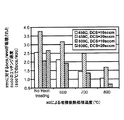
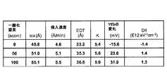
図6は、本発明により生成されるシリコン酸化膜とシリコン酸窒化膜の容量−電圧曲線を表している。シリコン酸化膜はDCSと水蒸気を用いて堆積された。シリコン酸窒化膜は、50sccmのNOガスを100sccmのDCSと水蒸気を加えることによって堆積された。図6と図7は、NOガスを加えることで、Tox、堆積速度、等価酸化膜厚さ(EOT)、及び誘電率(K)が増大することを示している。図7には図示されていないが、0〜50sccmのNOガス流については、界面トラップ密度(Dit)は、基本となるシリコン酸化膜の界面トラップ密度から約1/100に減少する−つまり−約1012eV-1cm-2から約1010eV-1cm-2に低下することが予想される。そのようにDitが減少することで、シリコン酸窒化膜の界面には電荷トラップが相対的に存在しないようになり、そのため、電子/正孔移動度とピークチャネル駆動電流が顕著に改善された金属−酸化物−半導体電界効果型トランジスタ(MOSFET)デバイスのゲート誘電体として有利に利用されうる。さらにNOガス流速が50sccmよりも大きな値にまで増大し、かつ、シリコン酸窒化膜中でのN濃度がさらに増大することで、Dit値が増大するにもかかわらず、シリコン酸窒化膜を含む半導体デバイス(たとえばフラッシュトンネルゲートのような不揮発性メモリ(NVM))の信頼性が改善される。Dit値の増大は、界面電荷トラップの可能性の増大とMOSFET閾値電圧(Vth)のシフトが起こりうることを示唆している一方で、NVMについての信頼性の改善は、Dit値の増大から生じる如何なる不利益をも大きく上回ると考えられる。N濃度の増大は、膜内部での緩やかな原子結合(ダングリングボンド)をより強く結合する上で有用と考えられる。さらにN濃度の増大は、膜の密度を増大させ、その結果、半導体処理において通常用いられる高電圧での電子衝突に対する耐性が増大する。全体として、結果は、従来のDCSとN2Oとの反応を用いるときとは異なり、DCSとH2Oを用いた成膜中にNOを加えることは、シリコン酸化膜にNを導入することで、半導体デバイス用のシリコン酸窒化膜を生成する上で有効であることを示している。 FIG. 6 shows a capacitance-voltage curve of the silicon oxide film and the silicon oxynitride film generated according to the present invention. The silicon oxide film was deposited using DCS and water vapor. The silicon oxynitride film was deposited by adding 50 sccm of NO gas and 100 sccm of DCS and water vapor. FIGS. 6 and 7 show that the addition of NO gas increases Tox , deposition rate, equivalent oxide thickness (EOT), and dielectric constant (K). Although not shown in FIG. 7, for a NO gas flow of 0-50 sccm, the interface trap density (D it ) decreases to about 1/100 from the interface trap density of the basic silicon oxide film—that is— It is expected to drop from about 10 12 eV −1 cm −2 to about 10 10 eV −1 cm −2 . By so D it is reduced, the interface between the silicon oxynitride film become the charge trapping relative absence, therefore, the electron / hole mobility and peak channel drive current is significantly improved It can be advantageously used as a gate dielectric in metal-oxide-semiconductor field effect transistor (MOSFET) devices. In addition, the NO gas flow rate increases to a value larger than 50 sccm, and the N concentration in the silicon oxynitride film further increases, so that the Dit value increases, but the silicon oxynitride film is included. Reliability of semiconductor devices (eg, non-volatile memory (NVM) such as flash tunnel gates) is improved. Increase in D it value, while suggesting that the shift of increasing the MOSFET threshold voltage of the possibility of interface charge trapping (V th) can occur, improving the reliability of the NVM is the D it value It is considered that it will greatly surpass any disadvantage resulting from the increase. An increase in N concentration is considered useful for stronger bonding of loose atomic bonds (dangling bonds) inside the film. Further, increasing the N concentration increases the density of the film, resulting in an increase in resistance to electron collisions at high voltages typically used in semiconductor processing. Overall, the results are different from using the reaction of conventional DCS and N 2 O, and adding NO during deposition using DCS and H 2 O introduces N into the silicon oxide film This shows that it is effective in producing a silicon oxynitride film for a semiconductor device.
Claims (18)
プロセスチャンバ内に複数の基板を設置する工程;
前記プロセスチャンバを400℃乃至650℃未満の堆積温度にまで加熱する工程;
前記プロセスチャンバへ水蒸気を含む第1プロセスガスを流入させる工程;
前記プロセスチャンバへジクロロシラン(DCS)を含む第2プロセスガスを流入させる工程;
ガス圧力を2Torr未満に設定する工程;及び、
前記第1プロセスガスと前記第2プロセスガスとを反応させて前記複数の基板上にシリコン酸化膜を熱的に堆積する工程;
を有する方法。 A method of depositing a dielectric film on a substrate comprising:
Installing a plurality of substrates in a process chamber;
Heating the process chamber to a deposition temperature of 400 ° C. to less than 650 ° C .;
Flowing a first process gas containing water vapor into the process chamber;
Flowing a second process gas containing dichlorosilane (DCS) into the process chamber;
Setting the gas pressure to less than 2 Torr; and
Reacting the first process gas and the second process gas to thermally deposit a silicon oxide film on the plurality of substrates;
Having a method.
前記シリコン酸化膜と前記第3プロセスガスとを反応させることで、前記基板上にシリコン酸窒化膜を生成する工程;
をさらに有する、請求項1に記載の方法。 Flowing a third process gas containing nitric oxide (NO) into the process chamber while flowing the first process gas and the second process gas; and reacting the silicon oxide film with the third process gas A step of generating a silicon oxynitride film on the substrate;
The method of claim 1, further comprising:
前記シリコン酸化膜へのNの導入を制御するように前記第3プロセスガスを流しながら、第2希釈ガスを前記プロセスチャンバへ流入させる工程;
をさらに有する、請求項6に記載の方法。 Introducing a first dilution gas into the process chamber while flowing the first process gas and the second process gas so as to control the growth rate of the silicon oxide film; and introducing N into the silicon oxide film; Flowing a second dilution gas into the process chamber while flowing the third process gas to control
The method of claim 6, further comprising:
プロセスチャンバ内に複数の基板を設置する工程;
前記プロセスチャンバを400℃乃至650℃未満の堆積温度にまで加熱する工程;
前記プロセスチャンバへ水蒸気を含む第1プロセスガスを流入させる工程であって、前記水蒸気は水素ガス(H2)と酸素ガス(O2)との燃焼によって前記プロセスチャンバの外部で生成される、工程;
前記プロセスチャンバへジクロロシラン(DCS)を含む第2プロセスガスを流入させる工程;
前記プロセスチャンバ内でのガス圧力を2Torr未満に設定する工程;
前記第1プロセスガスと前記第2プロセスガスとを反応させて前記複数の基板上にシリコン酸化膜を熱的に堆積する工程;並びに、
前記シリコン酸化膜の生成後、窒素(N2)、一酸化窒素(NO)、亜酸化窒素(N2O)、酸素(O2)、及び/又は水(H2O)のうちの少なくとも1つを有する熱処理ガス内において上に前記シリコン酸化膜を有する前記基板を熱処理する工程であって、前記熱処理は前記堆積温度よりも高い温度で実行される、工程;
を有する方法。 A method of depositing a dielectric film on a substrate comprising:
Installing a plurality of substrates in a process chamber;
Heating the process chamber to a deposition temperature of 400 ° C. to less than 650 ° C .;
Flowing a first process gas containing water vapor into the process chamber, wherein the water vapor is generated outside the process chamber by combustion of hydrogen gas (H 2 ) and oxygen gas (O 2 ). ;
Flowing a second process gas containing dichlorosilane (DCS) into the process chamber;
Setting the gas pressure in the process chamber to less than 2 Torr;
Reacting the first process gas and the second process gas to thermally deposit a silicon oxide film on the plurality of substrates; and
After the formation of the silicon oxide film, at least one of nitrogen (N 2 ), nitric oxide (NO), nitrous oxide (N 2 O), oxygen (O 2 ), and / or water (H 2 O). A step of heat-treating the substrate having the silicon oxide film thereon in a heat treatment gas having a temperature, wherein the heat treatment is performed at a temperature higher than the deposition temperature;
Having a method.
プロセスチャンバ内に複数の基板を設置する工程;
前記プロセスチャンバを400℃乃至650℃未満の堆積温度にまで加熱する工程;
前記プロセスチャンバへ水蒸気を含む第1プロセスガスを流入させる工程であって、前記水蒸気は水素ガス(H2)と酸素ガス(O2)との燃焼によって前記プロセスチャンバの外部で生成される、工程;
前記プロセスチャンバへジクロロシラン(DCS)を含む第2プロセスガスを流入させる工程;
前記プロセスチャンバ内でのガス圧力を2Torr未満に設定する工程;
前記第1プロセスガスと前記第2プロセスガスとを反応させて前記複数の基板上にシリコン酸化膜を熱的に堆積する工程;並びに、
前記シリコン酸窒化膜の生成後、窒素(N2)、一酸化窒素(NO)、亜酸化窒素(N2O)、酸素(O2)、及び/又は水(H2O)のうちの少なくとも1つを有する熱処理ガス内において上に前記シリコン酸窒化膜を有する前記基板を熱処理する工程;
を有する方法。 A method of depositing a dielectric film on a substrate comprising:
Installing a plurality of substrates in a process chamber;
Heating the process chamber to a deposition temperature of 400 ° C. to less than 650 ° C .;
Flowing a first process gas containing water vapor into the process chamber, wherein the water vapor is generated outside the process chamber by combustion of hydrogen gas (H 2 ) and oxygen gas (O 2 ). ;
Flowing a second process gas containing dichlorosilane (DCS) into the process chamber;
Setting the gas pressure in the process chamber to less than 2 Torr;
Reacting the first process gas and the second process gas to thermally deposit a silicon oxide film on the plurality of substrates; and
After the formation of the silicon oxynitride film, at least one of nitrogen (N 2 ), nitric oxide (NO), nitrous oxide (N 2 O), oxygen (O 2 ), and / or water (H 2 O) Heat treating the substrate having the silicon oxynitride film thereon in a heat treatment gas having one;
Having a method.
前記シリコン酸化膜への窒素の導入を制御するように前記第3プロセスガスを流しながら、第2希釈ガスを前記プロセスチャンバへ流入させる工程;
をさらに有する、請求項14に記載の方法。 Flowing a first dilution gas into the process chamber while flowing the first process gas and the second process gas so as to control the growth rate of the silicon oxide film; and introducing nitrogen into the silicon oxide film; Flowing a second dilution gas into the process chamber while flowing the third process gas to control
15. The method of claim 14, further comprising:
Applications Claiming Priority (3)
| Application Number | Priority Date | Filing Date | Title |
|---|---|---|---|
| US12/894,513 US7994070B1 (en) | 2010-09-30 | 2010-09-30 | Low-temperature dielectric film formation by chemical vapor deposition |
| US12/894,513 | 2010-09-30 | ||
| PCT/US2011/053503 WO2012044622A2 (en) | 2010-09-30 | 2011-09-27 | Low-temperature dielectric film formation by chemical vapor deposition |
Publications (2)
| Publication Number | Publication Date |
|---|---|
| JP2013545275A true JP2013545275A (en) | 2013-12-19 |
| JP2013545275A5 JP2013545275A5 (en) | 2014-07-10 |
Family
ID=44350747
Family Applications (1)
| Application Number | Title | Priority Date | Filing Date |
|---|---|---|---|
| JP2013531729A Pending JP2013545275A (en) | 2010-09-30 | 2011-09-27 | Preparation of dielectric films at low temperatures by chemical vapor deposition |
Country Status (5)
| Country | Link |
|---|---|
| US (1) | US7994070B1 (en) |
| JP (1) | JP2013545275A (en) |
| KR (1) | KR20130140696A (en) |
| TW (1) | TWI464802B (en) |
| WO (1) | WO2012044622A2 (en) |
Families Citing this family (251)
| Publication number | Priority date | Publication date | Assignee | Title |
|---|---|---|---|---|
| US9394608B2 (en) | 2009-04-06 | 2016-07-19 | Asm America, Inc. | Semiconductor processing reactor and components thereof |
| US8802201B2 (en) | 2009-08-14 | 2014-08-12 | Asm America, Inc. | Systems and methods for thin-film deposition of metal oxides using excited nitrogen-oxygen species |
| US9312155B2 (en) | 2011-06-06 | 2016-04-12 | Asm Japan K.K. | High-throughput semiconductor-processing apparatus equipped with multiple dual-chamber modules |
| US10854498B2 (en) | 2011-07-15 | 2020-12-01 | Asm Ip Holding B.V. | Wafer-supporting device and method for producing same |
| US20130023129A1 (en) | 2011-07-20 | 2013-01-24 | Asm America, Inc. | Pressure transmitter for a semiconductor processing environment |
| US9017481B1 (en) | 2011-10-28 | 2015-04-28 | Asm America, Inc. | Process feed management for semiconductor substrate processing |
| US10714315B2 (en) | 2012-10-12 | 2020-07-14 | Asm Ip Holdings B.V. | Semiconductor reaction chamber showerhead |
| US20140216498A1 (en) * | 2013-02-06 | 2014-08-07 | Kwangduk Douglas Lee | Methods of dry stripping boron-carbon films |
| US10683571B2 (en) | 2014-02-25 | 2020-06-16 | Asm Ip Holding B.V. | Gas supply manifold and method of supplying gases to chamber using same |
| US10167557B2 (en) | 2014-03-18 | 2019-01-01 | Asm Ip Holding B.V. | Gas distribution system, reactor including the system, and methods of using the same |
| US11015245B2 (en) | 2014-03-19 | 2021-05-25 | Asm Ip Holding B.V. | Gas-phase reactor and system having exhaust plenum and components thereof |
| US10858737B2 (en) | 2014-07-28 | 2020-12-08 | Asm Ip Holding B.V. | Showerhead assembly and components thereof |
| US9890456B2 (en) | 2014-08-21 | 2018-02-13 | Asm Ip Holding B.V. | Method and system for in situ formation of gas-phase compounds |
| US10941490B2 (en) | 2014-10-07 | 2021-03-09 | Asm Ip Holding B.V. | Multiple temperature range susceptor, assembly, reactor and system including the susceptor, and methods of using the same |
| US9657845B2 (en) | 2014-10-07 | 2017-05-23 | Asm Ip Holding B.V. | Variable conductance gas distribution apparatus and method |
| US10276355B2 (en) | 2015-03-12 | 2019-04-30 | Asm Ip Holding B.V. | Multi-zone reactor, system including the reactor, and method of using the same |
| US10458018B2 (en) | 2015-06-26 | 2019-10-29 | Asm Ip Holding B.V. | Structures including metal carbide material, devices including the structures, and methods of forming same |
| US10600673B2 (en) | 2015-07-07 | 2020-03-24 | Asm Ip Holding B.V. | Magnetic susceptor to baseplate seal |
| US10211308B2 (en) | 2015-10-21 | 2019-02-19 | Asm Ip Holding B.V. | NbMC layers |
| US11139308B2 (en) | 2015-12-29 | 2021-10-05 | Asm Ip Holding B.V. | Atomic layer deposition of III-V compounds to form V-NAND devices |
| US10529554B2 (en) | 2016-02-19 | 2020-01-07 | Asm Ip Holding B.V. | Method for forming silicon nitride film selectively on sidewalls or flat surfaces of trenches |
| US10865475B2 (en) | 2016-04-21 | 2020-12-15 | Asm Ip Holding B.V. | Deposition of metal borides and silicides |
| US10190213B2 (en) | 2016-04-21 | 2019-01-29 | Asm Ip Holding B.V. | Deposition of metal borides |
| US10367080B2 (en) | 2016-05-02 | 2019-07-30 | Asm Ip Holding B.V. | Method of forming a germanium oxynitride film |
| US10032628B2 (en) | 2016-05-02 | 2018-07-24 | Asm Ip Holding B.V. | Source/drain performance through conformal solid state doping |
| US11453943B2 (en) | 2016-05-25 | 2022-09-27 | Asm Ip Holding B.V. | Method for forming carbon-containing silicon/metal oxide or nitride film by ALD using silicon precursor and hydrocarbon precursor |
| US9859151B1 (en) | 2016-07-08 | 2018-01-02 | Asm Ip Holding B.V. | Selective film deposition method to form air gaps |
| US10612137B2 (en) | 2016-07-08 | 2020-04-07 | Asm Ip Holdings B.V. | Organic reactants for atomic layer deposition |
| US10714385B2 (en) | 2016-07-19 | 2020-07-14 | Asm Ip Holding B.V. | Selective deposition of tungsten |
| US9887082B1 (en) | 2016-07-28 | 2018-02-06 | Asm Ip Holding B.V. | Method and apparatus for filling a gap |
| US9812320B1 (en) | 2016-07-28 | 2017-11-07 | Asm Ip Holding B.V. | Method and apparatus for filling a gap |
| KR102532607B1 (en) | 2016-07-28 | 2023-05-15 | 에이에스엠 아이피 홀딩 비.브이. | Substrate processing apparatus and method of operating the same |
| US10643826B2 (en) | 2016-10-26 | 2020-05-05 | Asm Ip Holdings B.V. | Methods for thermally calibrating reaction chambers |
| US11532757B2 (en) | 2016-10-27 | 2022-12-20 | Asm Ip Holding B.V. | Deposition of charge trapping layers |
| US10229833B2 (en) | 2016-11-01 | 2019-03-12 | Asm Ip Holding B.V. | Methods for forming a transition metal nitride film on a substrate by atomic layer deposition and related semiconductor device structures |
| US10643904B2 (en) | 2016-11-01 | 2020-05-05 | Asm Ip Holdings B.V. | Methods for forming a semiconductor device and related semiconductor device structures |
| US10714350B2 (en) | 2016-11-01 | 2020-07-14 | ASM IP Holdings, B.V. | Methods for forming a transition metal niobium nitride film on a substrate by atomic layer deposition and related semiconductor device structures |
| US10134757B2 (en) | 2016-11-07 | 2018-11-20 | Asm Ip Holding B.V. | Method of processing a substrate and a device manufactured by using the method |
| KR102546317B1 (en) | 2016-11-15 | 2023-06-21 | 에이에스엠 아이피 홀딩 비.브이. | Gas supply unit and substrate processing apparatus including the same |
| KR20180068582A (en) | 2016-12-14 | 2018-06-22 | 에이에스엠 아이피 홀딩 비.브이. | Substrate processing apparatus |
| US11581186B2 (en) | 2016-12-15 | 2023-02-14 | Asm Ip Holding B.V. | Sequential infiltration synthesis apparatus |
| US11447861B2 (en) | 2016-12-15 | 2022-09-20 | Asm Ip Holding B.V. | Sequential infiltration synthesis apparatus and a method of forming a patterned structure |
| KR20180070971A (en) | 2016-12-19 | 2018-06-27 | 에이에스엠 아이피 홀딩 비.브이. | Substrate processing apparatus |
| US10269558B2 (en) | 2016-12-22 | 2019-04-23 | Asm Ip Holding B.V. | Method of forming a structure on a substrate |
| US10867788B2 (en) | 2016-12-28 | 2020-12-15 | Asm Ip Holding B.V. | Method of forming a structure on a substrate |
| US11390950B2 (en) | 2017-01-10 | 2022-07-19 | Asm Ip Holding B.V. | Reactor system and method to reduce residue buildup during a film deposition process |
| US10655221B2 (en) | 2017-02-09 | 2020-05-19 | Asm Ip Holding B.V. | Method for depositing oxide film by thermal ALD and PEALD |
| US10468261B2 (en) | 2017-02-15 | 2019-11-05 | Asm Ip Holding B.V. | Methods for forming a metallic film on a substrate by cyclical deposition and related semiconductor device structures |
| US10529563B2 (en) | 2017-03-29 | 2020-01-07 | Asm Ip Holdings B.V. | Method for forming doped metal oxide films on a substrate by cyclical deposition and related semiconductor device structures |
| USD876504S1 (en) | 2017-04-03 | 2020-02-25 | Asm Ip Holding B.V. | Exhaust flow control ring for semiconductor deposition apparatus |
| KR102457289B1 (en) | 2017-04-25 | 2022-10-21 | 에이에스엠 아이피 홀딩 비.브이. | Method for depositing a thin film and manufacturing a semiconductor device |
| US10892156B2 (en) | 2017-05-08 | 2021-01-12 | Asm Ip Holding B.V. | Methods for forming a silicon nitride film on a substrate and related semiconductor device structures |
| US10770286B2 (en) | 2017-05-08 | 2020-09-08 | Asm Ip Holdings B.V. | Methods for selectively forming a silicon nitride film on a substrate and related semiconductor device structures |
| US11306395B2 (en) | 2017-06-28 | 2022-04-19 | Asm Ip Holding B.V. | Methods for depositing a transition metal nitride film on a substrate by atomic layer deposition and related deposition apparatus |
| US10685834B2 (en) | 2017-07-05 | 2020-06-16 | Asm Ip Holdings B.V. | Methods for forming a silicon germanium tin layer and related semiconductor device structures |
| KR20190009245A (en) | 2017-07-18 | 2019-01-28 | 에이에스엠 아이피 홀딩 비.브이. | Methods for forming a semiconductor device structure and related semiconductor device structures |
| US11018002B2 (en) | 2017-07-19 | 2021-05-25 | Asm Ip Holding B.V. | Method for selectively depositing a Group IV semiconductor and related semiconductor device structures |
| US11374112B2 (en) | 2017-07-19 | 2022-06-28 | Asm Ip Holding B.V. | Method for depositing a group IV semiconductor and related semiconductor device structures |
| US10541333B2 (en) | 2017-07-19 | 2020-01-21 | Asm Ip Holding B.V. | Method for depositing a group IV semiconductor and related semiconductor device structures |
| US10590535B2 (en) | 2017-07-26 | 2020-03-17 | Asm Ip Holdings B.V. | Chemical treatment, deposition and/or infiltration apparatus and method for using the same |
| US10692741B2 (en) | 2017-08-08 | 2020-06-23 | Asm Ip Holdings B.V. | Radiation shield |
| US10770336B2 (en) | 2017-08-08 | 2020-09-08 | Asm Ip Holding B.V. | Substrate lift mechanism and reactor including same |
| US10249524B2 (en) | 2017-08-09 | 2019-04-02 | Asm Ip Holding B.V. | Cassette holder assembly for a substrate cassette and holding member for use in such assembly |
| US11139191B2 (en) | 2017-08-09 | 2021-10-05 | Asm Ip Holding B.V. | Storage apparatus for storing cassettes for substrates and processing apparatus equipped therewith |
| US11769682B2 (en) | 2017-08-09 | 2023-09-26 | Asm Ip Holding B.V. | Storage apparatus for storing cassettes for substrates and processing apparatus equipped therewith |
| USD900036S1 (en) | 2017-08-24 | 2020-10-27 | Asm Ip Holding B.V. | Heater electrical connector and adapter |
| US11830730B2 (en) | 2017-08-29 | 2023-11-28 | Asm Ip Holding B.V. | Layer forming method and apparatus |
| US11056344B2 (en) | 2017-08-30 | 2021-07-06 | Asm Ip Holding B.V. | Layer forming method |
| KR102491945B1 (en) | 2017-08-30 | 2023-01-26 | 에이에스엠 아이피 홀딩 비.브이. | Substrate processing apparatus |
| US11295980B2 (en) | 2017-08-30 | 2022-04-05 | Asm Ip Holding B.V. | Methods for depositing a molybdenum metal film over a dielectric surface of a substrate by a cyclical deposition process and related semiconductor device structures |
| KR102630301B1 (en) | 2017-09-21 | 2024-01-29 | 에이에스엠 아이피 홀딩 비.브이. | Method of sequential infiltration synthesis treatment of infiltrateable material and structures and devices formed using same |
| US10844484B2 (en) | 2017-09-22 | 2020-11-24 | Asm Ip Holding B.V. | Apparatus for dispensing a vapor phase reactant to a reaction chamber and related methods |
| US10658205B2 (en) | 2017-09-28 | 2020-05-19 | Asm Ip Holdings B.V. | Chemical dispensing apparatus and methods for dispensing a chemical to a reaction chamber |
| US10403504B2 (en) | 2017-10-05 | 2019-09-03 | Asm Ip Holding B.V. | Method for selectively depositing a metallic film on a substrate |
| US10319588B2 (en) | 2017-10-10 | 2019-06-11 | Asm Ip Holding B.V. | Method for depositing a metal chalcogenide on a substrate by cyclical deposition |
| US10923344B2 (en) | 2017-10-30 | 2021-02-16 | Asm Ip Holding B.V. | Methods for forming a semiconductor structure and related semiconductor structures |
| KR102443047B1 (en) | 2017-11-16 | 2022-09-14 | 에이에스엠 아이피 홀딩 비.브이. | Method of processing a substrate and a device manufactured by the same |
| US10910262B2 (en) | 2017-11-16 | 2021-02-02 | Asm Ip Holding B.V. | Method of selectively depositing a capping layer structure on a semiconductor device structure |
| US11022879B2 (en) | 2017-11-24 | 2021-06-01 | Asm Ip Holding B.V. | Method of forming an enhanced unexposed photoresist layer |
| KR102597978B1 (en) | 2017-11-27 | 2023-11-06 | 에이에스엠 아이피 홀딩 비.브이. | Storage device for storing wafer cassettes for use with batch furnaces |
| CN111344522B (en) | 2017-11-27 | 2022-04-12 | 阿斯莫Ip控股公司 | Including clean mini-environment device |
| US10872771B2 (en) | 2018-01-16 | 2020-12-22 | Asm Ip Holding B. V. | Method for depositing a material film on a substrate within a reaction chamber by a cyclical deposition process and related device structures |
| KR20200108016A (en) | 2018-01-19 | 2020-09-16 | 에이에스엠 아이피 홀딩 비.브이. | Method of depositing a gap fill layer by plasma assisted deposition |
| TWI799494B (en) | 2018-01-19 | 2023-04-21 | 荷蘭商Asm 智慧財產控股公司 | Deposition method |
| USD903477S1 (en) | 2018-01-24 | 2020-12-01 | Asm Ip Holdings B.V. | Metal clamp |
| US11018047B2 (en) | 2018-01-25 | 2021-05-25 | Asm Ip Holding B.V. | Hybrid lift pin |
| USD880437S1 (en) | 2018-02-01 | 2020-04-07 | Asm Ip Holding B.V. | Gas supply plate for semiconductor manufacturing apparatus |
| US11081345B2 (en) * | 2018-02-06 | 2021-08-03 | Asm Ip Holding B.V. | Method of post-deposition treatment for silicon oxide film |
| US11685991B2 (en) | 2018-02-14 | 2023-06-27 | Asm Ip Holding B.V. | Method for depositing a ruthenium-containing film on a substrate by a cyclical deposition process |
| US10896820B2 (en) | 2018-02-14 | 2021-01-19 | Asm Ip Holding B.V. | Method for depositing a ruthenium-containing film on a substrate by a cyclical deposition process |
| US10731249B2 (en) | 2018-02-15 | 2020-08-04 | Asm Ip Holding B.V. | Method of forming a transition metal containing film on a substrate by a cyclical deposition process, a method for supplying a transition metal halide compound to a reaction chamber, and related vapor deposition apparatus |
| KR102636427B1 (en) | 2018-02-20 | 2024-02-13 | 에이에스엠 아이피 홀딩 비.브이. | Substrate processing method and apparatus |
| US10658181B2 (en) | 2018-02-20 | 2020-05-19 | Asm Ip Holding B.V. | Method of spacer-defined direct patterning in semiconductor fabrication |
| US10975470B2 (en) | 2018-02-23 | 2021-04-13 | Asm Ip Holding B.V. | Apparatus for detecting or monitoring for a chemical precursor in a high temperature environment |
| US11473195B2 (en) | 2018-03-01 | 2022-10-18 | Asm Ip Holding B.V. | Semiconductor processing apparatus and a method for processing a substrate |
| US11629406B2 (en) | 2018-03-09 | 2023-04-18 | Asm Ip Holding B.V. | Semiconductor processing apparatus comprising one or more pyrometers for measuring a temperature of a substrate during transfer of the substrate |
| US11114283B2 (en) | 2018-03-16 | 2021-09-07 | Asm Ip Holding B.V. | Reactor, system including the reactor, and methods of manufacturing and using same |
| KR102646467B1 (en) | 2018-03-27 | 2024-03-11 | 에이에스엠 아이피 홀딩 비.브이. | Method of forming an electrode on a substrate and a semiconductor device structure including an electrode |
| US11230766B2 (en) | 2018-03-29 | 2022-01-25 | Asm Ip Holding B.V. | Substrate processing apparatus and method |
| US11088002B2 (en) | 2018-03-29 | 2021-08-10 | Asm Ip Holding B.V. | Substrate rack and a substrate processing system and method |
| KR102501472B1 (en) | 2018-03-30 | 2023-02-20 | 에이에스엠 아이피 홀딩 비.브이. | Substrate processing method |
| KR20190128558A (en) | 2018-05-08 | 2019-11-18 | 에이에스엠 아이피 홀딩 비.브이. | Methods for depositing an oxide film on a substrate by a cyclical deposition process and related device structures |
| TWI816783B (en) | 2018-05-11 | 2023-10-01 | 荷蘭商Asm 智慧財產控股公司 | Methods for forming a doped metal carbide film on a substrate and related semiconductor device structures |
| KR102596988B1 (en) | 2018-05-28 | 2023-10-31 | 에이에스엠 아이피 홀딩 비.브이. | Method of processing a substrate and a device manufactured by the same |
| TW202013553A (en) | 2018-06-04 | 2020-04-01 | 荷蘭商Asm 智慧財產控股公司 | Wafer handling chamber with moisture reduction |
| US11718913B2 (en) | 2018-06-04 | 2023-08-08 | Asm Ip Holding B.V. | Gas distribution system and reactor system including same |
| US11286562B2 (en) | 2018-06-08 | 2022-03-29 | Asm Ip Holding B.V. | Gas-phase chemical reactor and method of using same |
| US10797133B2 (en) | 2018-06-21 | 2020-10-06 | Asm Ip Holding B.V. | Method for depositing a phosphorus doped silicon arsenide film and related semiconductor device structures |
| KR102568797B1 (en) | 2018-06-21 | 2023-08-21 | 에이에스엠 아이피 홀딩 비.브이. | Substrate processing system |
| WO2020003000A1 (en) | 2018-06-27 | 2020-01-02 | Asm Ip Holding B.V. | Cyclic deposition methods for forming metal-containing material and films and structures including the metal-containing material |
| TWI819010B (en) | 2018-06-27 | 2023-10-21 | 荷蘭商Asm Ip私人控股有限公司 | Cyclic deposition methods for forming metal-containing material and films and structures including the metal-containing material |
| US10612136B2 (en) | 2018-06-29 | 2020-04-07 | ASM IP Holding, B.V. | Temperature-controlled flange and reactor system including same |
| KR20200002519A (en) | 2018-06-29 | 2020-01-08 | 에이에스엠 아이피 홀딩 비.브이. | Method for depositing a thin film and manufacturing a semiconductor device |
| US10388513B1 (en) | 2018-07-03 | 2019-08-20 | Asm Ip Holding B.V. | Method for depositing silicon-free carbon-containing film as gap-fill layer by pulse plasma-assisted deposition |
| US10755922B2 (en) | 2018-07-03 | 2020-08-25 | Asm Ip Holding B.V. | Method for depositing silicon-free carbon-containing film as gap-fill layer by pulse plasma-assisted deposition |
| US10767789B2 (en) | 2018-07-16 | 2020-09-08 | Asm Ip Holding B.V. | Diaphragm valves, valve components, and methods for forming valve components |
| US11053591B2 (en) | 2018-08-06 | 2021-07-06 | Asm Ip Holding B.V. | Multi-port gas injection system and reactor system including same |
| US10883175B2 (en) | 2018-08-09 | 2021-01-05 | Asm Ip Holding B.V. | Vertical furnace for processing substrates and a liner for use therein |
| US10829852B2 (en) | 2018-08-16 | 2020-11-10 | Asm Ip Holding B.V. | Gas distribution device for a wafer processing apparatus |
| US11430674B2 (en) | 2018-08-22 | 2022-08-30 | Asm Ip Holding B.V. | Sensor array, apparatus for dispensing a vapor phase reactant to a reaction chamber and related methods |
| US11024523B2 (en) | 2018-09-11 | 2021-06-01 | Asm Ip Holding B.V. | Substrate processing apparatus and method |
| KR20200030162A (en) | 2018-09-11 | 2020-03-20 | 에이에스엠 아이피 홀딩 비.브이. | Method for deposition of a thin film |
| US11049751B2 (en) | 2018-09-14 | 2021-06-29 | Asm Ip Holding B.V. | Cassette supply system to store and handle cassettes and processing apparatus equipped therewith |
| CN110970344A (en) | 2018-10-01 | 2020-04-07 | Asm Ip控股有限公司 | Substrate holding apparatus, system including the same, and method of using the same |
| US11232963B2 (en) | 2018-10-03 | 2022-01-25 | Asm Ip Holding B.V. | Substrate processing apparatus and method |
| KR102592699B1 (en) | 2018-10-08 | 2023-10-23 | 에이에스엠 아이피 홀딩 비.브이. | Substrate support unit and apparatuses for depositing thin film and processing the substrate including the same |
| US10847365B2 (en) | 2018-10-11 | 2020-11-24 | Asm Ip Holding B.V. | Method of forming conformal silicon carbide film by cyclic CVD |
| US10811256B2 (en) | 2018-10-16 | 2020-10-20 | Asm Ip Holding B.V. | Method for etching a carbon-containing feature |
| KR102605121B1 (en) | 2018-10-19 | 2023-11-23 | 에이에스엠 아이피 홀딩 비.브이. | Substrate processing apparatus and substrate processing method |
| KR102546322B1 (en) | 2018-10-19 | 2023-06-21 | 에이에스엠 아이피 홀딩 비.브이. | Substrate processing apparatus and substrate processing method |
| USD948463S1 (en) | 2018-10-24 | 2022-04-12 | Asm Ip Holding B.V. | Susceptor for semiconductor substrate supporting apparatus |
| US11087997B2 (en) | 2018-10-31 | 2021-08-10 | Asm Ip Holding B.V. | Substrate processing apparatus for processing substrates |
| KR20200051105A (en) | 2018-11-02 | 2020-05-13 | 에이에스엠 아이피 홀딩 비.브이. | Substrate support unit and substrate processing apparatus including the same |
| US11572620B2 (en) | 2018-11-06 | 2023-02-07 | Asm Ip Holding B.V. | Methods for selectively depositing an amorphous silicon film on a substrate |
| US11031242B2 (en) | 2018-11-07 | 2021-06-08 | Asm Ip Holding B.V. | Methods for depositing a boron doped silicon germanium film |
| US10847366B2 (en) | 2018-11-16 | 2020-11-24 | Asm Ip Holding B.V. | Methods for depositing a transition metal chalcogenide film on a substrate by a cyclical deposition process |
| US10818758B2 (en) | 2018-11-16 | 2020-10-27 | Asm Ip Holding B.V. | Methods for forming a metal silicate film on a substrate in a reaction chamber and related semiconductor device structures |
| US10559458B1 (en) | 2018-11-26 | 2020-02-11 | Asm Ip Holding B.V. | Method of forming oxynitride film |
| US11217444B2 (en) | 2018-11-30 | 2022-01-04 | Asm Ip Holding B.V. | Method for forming an ultraviolet radiation responsive metal oxide-containing film |
| KR102636428B1 (en) | 2018-12-04 | 2024-02-13 | 에이에스엠 아이피 홀딩 비.브이. | A method for cleaning a substrate processing apparatus |
| US11158513B2 (en) | 2018-12-13 | 2021-10-26 | Asm Ip Holding B.V. | Methods for forming a rhenium-containing film on a substrate by a cyclical deposition process and related semiconductor device structures |
| TW202037745A (en) | 2018-12-14 | 2020-10-16 | 荷蘭商Asm Ip私人控股有限公司 | Method of forming device structure, structure formed by the method and system for performing the method |
| TWI819180B (en) | 2019-01-17 | 2023-10-21 | 荷蘭商Asm 智慧財產控股公司 | Methods of forming a transition metal containing film on a substrate by a cyclical deposition process |
| KR20200091543A (en) | 2019-01-22 | 2020-07-31 | 에이에스엠 아이피 홀딩 비.브이. | Semiconductor processing device |
| CN111524788B (en) | 2019-02-01 | 2023-11-24 | Asm Ip私人控股有限公司 | Method for topologically selective film formation of silicon oxide |
| TW202104632A (en) | 2019-02-20 | 2021-02-01 | 荷蘭商Asm Ip私人控股有限公司 | Cyclical deposition method and apparatus for filling a recess formed within a substrate surface |
| KR102626263B1 (en) | 2019-02-20 | 2024-01-16 | 에이에스엠 아이피 홀딩 비.브이. | Cyclical deposition method including treatment step and apparatus for same |
| KR102638425B1 (en) | 2019-02-20 | 2024-02-21 | 에이에스엠 아이피 홀딩 비.브이. | Method and apparatus for filling a recess formed within a substrate surface |
| US11482533B2 (en) | 2019-02-20 | 2022-10-25 | Asm Ip Holding B.V. | Apparatus and methods for plug fill deposition in 3-D NAND applications |
| TW202100794A (en) | 2019-02-22 | 2021-01-01 | 荷蘭商Asm Ip私人控股有限公司 | Substrate processing apparatus and method for processing substrate |
| KR20200108248A (en) | 2019-03-08 | 2020-09-17 | 에이에스엠 아이피 홀딩 비.브이. | STRUCTURE INCLUDING SiOCN LAYER AND METHOD OF FORMING SAME |
| KR20200108242A (en) | 2019-03-08 | 2020-09-17 | 에이에스엠 아이피 홀딩 비.브이. | Method for Selective Deposition of Silicon Nitride Layer and Structure Including Selectively-Deposited Silicon Nitride Layer |
| KR20200108243A (en) | 2019-03-08 | 2020-09-17 | 에이에스엠 아이피 홀딩 비.브이. | Structure Including SiOC Layer and Method of Forming Same |
| JP2020167398A (en) | 2019-03-28 | 2020-10-08 | エーエスエム・アイピー・ホールディング・ベー・フェー | Door opener and substrate processing apparatus provided therewith |
| KR20200116855A (en) | 2019-04-01 | 2020-10-13 | 에이에스엠 아이피 홀딩 비.브이. | Method of manufacturing semiconductor device |
| KR20200123380A (en) | 2019-04-19 | 2020-10-29 | 에이에스엠 아이피 홀딩 비.브이. | Layer forming method and apparatus |
| KR20200125453A (en) | 2019-04-24 | 2020-11-04 | 에이에스엠 아이피 홀딩 비.브이. | Gas-phase reactor system and method of using same |
| KR20200130121A (en) | 2019-05-07 | 2020-11-18 | 에이에스엠 아이피 홀딩 비.브이. | Chemical source vessel with dip tube |
| KR20200130118A (en) | 2019-05-07 | 2020-11-18 | 에이에스엠 아이피 홀딩 비.브이. | Method for Reforming Amorphous Carbon Polymer Film |
| KR20200130652A (en) | 2019-05-10 | 2020-11-19 | 에이에스엠 아이피 홀딩 비.브이. | Method of depositing material onto a surface and structure formed according to the method |
| JP2020188255A (en) | 2019-05-16 | 2020-11-19 | エーエスエム アイピー ホールディング ビー.ブイ. | Wafer boat handling device, vertical batch furnace, and method |
| USD947913S1 (en) | 2019-05-17 | 2022-04-05 | Asm Ip Holding B.V. | Susceptor shaft |
| USD975665S1 (en) | 2019-05-17 | 2023-01-17 | Asm Ip Holding B.V. | Susceptor shaft |
| USD935572S1 (en) | 2019-05-24 | 2021-11-09 | Asm Ip Holding B.V. | Gas channel plate |
| USD922229S1 (en) | 2019-06-05 | 2021-06-15 | Asm Ip Holding B.V. | Device for controlling a temperature of a gas supply unit |
| KR20200141003A (en) | 2019-06-06 | 2020-12-17 | 에이에스엠 아이피 홀딩 비.브이. | Gas-phase reactor system including a gas detector |
| KR20200143254A (en) | 2019-06-11 | 2020-12-23 | 에이에스엠 아이피 홀딩 비.브이. | Method of forming an electronic structure using an reforming gas, system for performing the method, and structure formed using the method |
| USD944946S1 (en) | 2019-06-14 | 2022-03-01 | Asm Ip Holding B.V. | Shower plate |
| USD931978S1 (en) | 2019-06-27 | 2021-09-28 | Asm Ip Holding B.V. | Showerhead vacuum transport |
| KR20210005515A (en) | 2019-07-03 | 2021-01-14 | 에이에스엠 아이피 홀딩 비.브이. | Temperature control assembly for substrate processing apparatus and method of using same |
| JP2021015791A (en) | 2019-07-09 | 2021-02-12 | エーエスエム アイピー ホールディング ビー.ブイ. | Plasma device and substrate processing method using coaxial waveguide |
| CN112216646A (en) | 2019-07-10 | 2021-01-12 | Asm Ip私人控股有限公司 | Substrate supporting assembly and substrate processing device comprising same |
| KR20210010307A (en) | 2019-07-16 | 2021-01-27 | 에이에스엠 아이피 홀딩 비.브이. | Substrate processing apparatus |
| KR20210010820A (en) | 2019-07-17 | 2021-01-28 | 에이에스엠 아이피 홀딩 비.브이. | Methods of forming silicon germanium structures |
| KR20210010816A (en) | 2019-07-17 | 2021-01-28 | 에이에스엠 아이피 홀딩 비.브이. | Radical assist ignition plasma system and method |
| US11643724B2 (en) | 2019-07-18 | 2023-05-09 | Asm Ip Holding B.V. | Method of forming structures using a neutral beam |
| CN112242296A (en) | 2019-07-19 | 2021-01-19 | Asm Ip私人控股有限公司 | Method of forming topologically controlled amorphous carbon polymer films |
| CN112309843A (en) | 2019-07-29 | 2021-02-02 | Asm Ip私人控股有限公司 | Selective deposition method for achieving high dopant doping |
| CN112309899A (en) | 2019-07-30 | 2021-02-02 | Asm Ip私人控股有限公司 | Substrate processing apparatus |
| CN112309900A (en) | 2019-07-30 | 2021-02-02 | Asm Ip私人控股有限公司 | Substrate processing apparatus |
| US11587815B2 (en) | 2019-07-31 | 2023-02-21 | Asm Ip Holding B.V. | Vertical batch furnace assembly |
| US11227782B2 (en) | 2019-07-31 | 2022-01-18 | Asm Ip Holding B.V. | Vertical batch furnace assembly |
| US11587814B2 (en) | 2019-07-31 | 2023-02-21 | Asm Ip Holding B.V. | Vertical batch furnace assembly |
| CN112323048B (en) | 2019-08-05 | 2024-02-09 | Asm Ip私人控股有限公司 | Liquid level sensor for chemical source container |
| USD965044S1 (en) | 2019-08-19 | 2022-09-27 | Asm Ip Holding B.V. | Susceptor shaft |
| USD965524S1 (en) | 2019-08-19 | 2022-10-04 | Asm Ip Holding B.V. | Susceptor support |
| JP2021031769A (en) | 2019-08-21 | 2021-03-01 | エーエスエム アイピー ホールディング ビー.ブイ. | Production apparatus of mixed gas of film deposition raw material and film deposition apparatus |
| USD979506S1 (en) | 2019-08-22 | 2023-02-28 | Asm Ip Holding B.V. | Insulator |
| USD940837S1 (en) | 2019-08-22 | 2022-01-11 | Asm Ip Holding B.V. | Electrode |
| USD930782S1 (en) | 2019-08-22 | 2021-09-14 | Asm Ip Holding B.V. | Gas distributor |
| USD949319S1 (en) | 2019-08-22 | 2022-04-19 | Asm Ip Holding B.V. | Exhaust duct |
| KR20210024423A (en) | 2019-08-22 | 2021-03-05 | 에이에스엠 아이피 홀딩 비.브이. | Method for forming a structure with a hole |
| US11286558B2 (en) | 2019-08-23 | 2022-03-29 | Asm Ip Holding B.V. | Methods for depositing a molybdenum nitride film on a surface of a substrate by a cyclical deposition process and related semiconductor device structures including a molybdenum nitride film |
| KR20210024420A (en) | 2019-08-23 | 2021-03-05 | 에이에스엠 아이피 홀딩 비.브이. | Method for depositing silicon oxide film having improved quality by peald using bis(diethylamino)silane |
| KR20210029090A (en) | 2019-09-04 | 2021-03-15 | 에이에스엠 아이피 홀딩 비.브이. | Methods for selective deposition using a sacrificial capping layer |
| KR20210029663A (en) | 2019-09-05 | 2021-03-16 | 에이에스엠 아이피 홀딩 비.브이. | Substrate processing apparatus |
| US11562901B2 (en) | 2019-09-25 | 2023-01-24 | Asm Ip Holding B.V. | Substrate processing method |
| CN112593212B (en) | 2019-10-02 | 2023-12-22 | Asm Ip私人控股有限公司 | Method for forming topologically selective silicon oxide film by cyclic plasma enhanced deposition process |
| TW202129060A (en) | 2019-10-08 | 2021-08-01 | 荷蘭商Asm Ip控股公司 | Substrate processing device, and substrate processing method |
| KR20210043460A (en) | 2019-10-10 | 2021-04-21 | 에이에스엠 아이피 홀딩 비.브이. | Method of forming a photoresist underlayer and structure including same |
| KR20210045930A (en) | 2019-10-16 | 2021-04-27 | 에이에스엠 아이피 홀딩 비.브이. | Method of Topology-Selective Film Formation of Silicon Oxide |
| US11637014B2 (en) | 2019-10-17 | 2023-04-25 | Asm Ip Holding B.V. | Methods for selective deposition of doped semiconductor material |
| KR20210047808A (en) | 2019-10-21 | 2021-04-30 | 에이에스엠 아이피 홀딩 비.브이. | Apparatus and methods for selectively etching films |
| US11646205B2 (en) | 2019-10-29 | 2023-05-09 | Asm Ip Holding B.V. | Methods of selectively forming n-type doped material on a surface, systems for selectively forming n-type doped material, and structures formed using same |
| KR20210054983A (en) | 2019-11-05 | 2021-05-14 | 에이에스엠 아이피 홀딩 비.브이. | Structures with doped semiconductor layers and methods and systems for forming same |
| US11501968B2 (en) | 2019-11-15 | 2022-11-15 | Asm Ip Holding B.V. | Method for providing a semiconductor device with silicon filled gaps |
| KR20210062561A (en) | 2019-11-20 | 2021-05-31 | 에이에스엠 아이피 홀딩 비.브이. | Method of depositing carbon-containing material on a surface of a substrate, structure formed using the method, and system for forming the structure |
| KR20210065848A (en) | 2019-11-26 | 2021-06-04 | 에이에스엠 아이피 홀딩 비.브이. | Methods for selectivley forming a target film on a substrate comprising a first dielectric surface and a second metallic surface |
| CN112951697A (en) | 2019-11-26 | 2021-06-11 | Asm Ip私人控股有限公司 | Substrate processing apparatus |
| CN112885692A (en) | 2019-11-29 | 2021-06-01 | Asm Ip私人控股有限公司 | Substrate processing apparatus |
| CN112885693A (en) | 2019-11-29 | 2021-06-01 | Asm Ip私人控股有限公司 | Substrate processing apparatus |
| JP2021090042A (en) | 2019-12-02 | 2021-06-10 | エーエスエム アイピー ホールディング ビー.ブイ. | Substrate processing apparatus and substrate processing method |
| KR20210070898A (en) | 2019-12-04 | 2021-06-15 | 에이에스엠 아이피 홀딩 비.브이. | Substrate processing apparatus |
| KR20210078405A (en) | 2019-12-17 | 2021-06-28 | 에이에스엠 아이피 홀딩 비.브이. | Method of forming vanadium nitride layer and structure including the vanadium nitride layer |
| KR20210080214A (en) | 2019-12-19 | 2021-06-30 | 에이에스엠 아이피 홀딩 비.브이. | Methods for filling a gap feature on a substrate and related semiconductor structures |
| KR20210095050A (en) | 2020-01-20 | 2021-07-30 | 에이에스엠 아이피 홀딩 비.브이. | Method of forming thin film and method of modifying surface of thin film |
| TW202130846A (en) | 2020-02-03 | 2021-08-16 | 荷蘭商Asm Ip私人控股有限公司 | Method of forming structures including a vanadium or indium layer |
| KR20210100010A (en) | 2020-02-04 | 2021-08-13 | 에이에스엠 아이피 홀딩 비.브이. | Method and apparatus for transmittance measurements of large articles |
| US11776846B2 (en) | 2020-02-07 | 2023-10-03 | Asm Ip Holding B.V. | Methods for depositing gap filling fluids and related systems and devices |
| TW202146715A (en) | 2020-02-17 | 2021-12-16 | 荷蘭商Asm Ip私人控股有限公司 | Method for growing phosphorous-doped silicon layer and system of the same |
| US11876356B2 (en) | 2020-03-11 | 2024-01-16 | Asm Ip Holding B.V. | Lockout tagout assembly and system and method of using same |
| KR20210116240A (en) | 2020-03-11 | 2021-09-27 | 에이에스엠 아이피 홀딩 비.브이. | Substrate handling device with adjustable joints |
| KR20210124042A (en) | 2020-04-02 | 2021-10-14 | 에이에스엠 아이피 홀딩 비.브이. | Thin film forming method |
| TW202146689A (en) | 2020-04-03 | 2021-12-16 | 荷蘭商Asm Ip控股公司 | Method for forming barrier layer and method for manufacturing semiconductor device |
| TW202145344A (en) | 2020-04-08 | 2021-12-01 | 荷蘭商Asm Ip私人控股有限公司 | Apparatus and methods for selectively etching silcon oxide films |
| US11821078B2 (en) | 2020-04-15 | 2023-11-21 | Asm Ip Holding B.V. | Method for forming precoat film and method for forming silicon-containing film |
| JP2021172884A (en) | 2020-04-24 | 2021-11-01 | エーエスエム・アイピー・ホールディング・ベー・フェー | Method of forming vanadium nitride-containing layer and structure comprising vanadium nitride-containing layer |
| KR20210132600A (en) | 2020-04-24 | 2021-11-04 | 에이에스엠 아이피 홀딩 비.브이. | Methods and systems for depositing a layer comprising vanadium, nitrogen, and a further element |
| TW202146831A (en) | 2020-04-24 | 2021-12-16 | 荷蘭商Asm Ip私人控股有限公司 | Vertical batch furnace assembly, and method for cooling vertical batch furnace |
| KR20210134869A (en) | 2020-05-01 | 2021-11-11 | 에이에스엠 아이피 홀딩 비.브이. | Fast FOUP swapping with a FOUP handler |
| KR20210141379A (en) | 2020-05-13 | 2021-11-23 | 에이에스엠 아이피 홀딩 비.브이. | Laser alignment fixture for a reactor system |
| KR20210143653A (en) | 2020-05-19 | 2021-11-29 | 에이에스엠 아이피 홀딩 비.브이. | Substrate processing apparatus |
| KR20210145078A (en) | 2020-05-21 | 2021-12-01 | 에이에스엠 아이피 홀딩 비.브이. | Structures including multiple carbon layers and methods of forming and using same |
| TW202201602A (en) | 2020-05-29 | 2022-01-01 | 荷蘭商Asm Ip私人控股有限公司 | Substrate processing device |
| TW202218133A (en) | 2020-06-24 | 2022-05-01 | 荷蘭商Asm Ip私人控股有限公司 | Method for forming a layer provided with silicon |
| TW202217953A (en) | 2020-06-30 | 2022-05-01 | 荷蘭商Asm Ip私人控股有限公司 | Substrate processing method |
| KR20220010438A (en) | 2020-07-17 | 2022-01-25 | 에이에스엠 아이피 홀딩 비.브이. | Structures and methods for use in photolithography |
| TW202204662A (en) | 2020-07-20 | 2022-02-01 | 荷蘭商Asm Ip私人控股有限公司 | Method and system for depositing molybdenum layers |
| KR20220027026A (en) | 2020-08-26 | 2022-03-07 | 에이에스엠 아이피 홀딩 비.브이. | Method and system for forming metal silicon oxide and metal silicon oxynitride |
| USD990534S1 (en) | 2020-09-11 | 2023-06-27 | Asm Ip Holding B.V. | Weighted lift pin |
| USD1012873S1 (en) | 2020-09-24 | 2024-01-30 | Asm Ip Holding B.V. | Electrode for semiconductor processing apparatus |
| TW202229613A (en) | 2020-10-14 | 2022-08-01 | 荷蘭商Asm Ip私人控股有限公司 | Method of depositing material on stepped structure |
| TW202217037A (en) | 2020-10-22 | 2022-05-01 | 荷蘭商Asm Ip私人控股有限公司 | Method of depositing vanadium metal, structure, device and a deposition assembly |
| TW202223136A (en) | 2020-10-28 | 2022-06-16 | 荷蘭商Asm Ip私人控股有限公司 | Method for forming layer on substrate, and semiconductor processing system |
| KR20220076343A (en) | 2020-11-30 | 2022-06-08 | 에이에스엠 아이피 홀딩 비.브이. | an injector configured for arrangement within a reaction chamber of a substrate processing apparatus |
| CN114639631A (en) | 2020-12-16 | 2022-06-17 | Asm Ip私人控股有限公司 | Fixing device for measuring jumping and swinging |
| TW202231903A (en) | 2020-12-22 | 2022-08-16 | 荷蘭商Asm Ip私人控股有限公司 | Transition metal deposition method, transition metal layer, and deposition assembly for depositing transition metal on substrate |
| USD980813S1 (en) | 2021-05-11 | 2023-03-14 | Asm Ip Holding B.V. | Gas flow control plate for substrate processing apparatus |
| USD980814S1 (en) | 2021-05-11 | 2023-03-14 | Asm Ip Holding B.V. | Gas distributor for substrate processing apparatus |
| USD981973S1 (en) | 2021-05-11 | 2023-03-28 | Asm Ip Holding B.V. | Reactor wall for substrate processing apparatus |
| USD990441S1 (en) | 2021-09-07 | 2023-06-27 | Asm Ip Holding B.V. | Gas flow control plate |
Citations (7)
| Publication number | Priority date | Publication date | Assignee | Title |
|---|---|---|---|---|
| JP2001085428A (en) * | 1999-09-14 | 2001-03-30 | Hitachi Kokusai Electric Inc | Method for treating substrate |
| JP2001338923A (en) * | 2000-05-29 | 2001-12-07 | Tokyo Electron Ltd | Method for forming oxynitride film and apparatus for forming oxynitride film |
| JP2002289846A (en) * | 2001-03-28 | 2002-10-04 | Sony Corp | Semiconductor device and manufacturing method therefor |
| JP2003096566A (en) * | 2001-04-13 | 2003-04-03 | Zarlink Semiconductor Inc | Optical quality silica film |
| JP2005203730A (en) * | 2003-12-18 | 2005-07-28 | Seiko Epson Corp | Insulating film, semiconductor element, electron device, and electronic apparatus |
| JP2006086521A (en) * | 2004-08-27 | 2006-03-30 | Asm America Inc | Remote plasma activated nitridation |
| JP2008159639A (en) * | 2006-12-20 | 2008-07-10 | Seiko Epson Corp | Gate insulating film, method of evaluating gate insulating film, semiconductor element, electronic device, and electronic apparatus |
Family Cites Families (10)
| Publication number | Priority date | Publication date | Assignee | Title |
|---|---|---|---|---|
| TW578214B (en) * | 2000-05-29 | 2004-03-01 | Tokyo Electron Ltd | Method of forming oxynitride film or the like and system for carrying out the same |
| US6613695B2 (en) * | 2000-11-24 | 2003-09-02 | Asm America, Inc. | Surface preparation prior to deposition |
| JP4021653B2 (en) | 2001-11-30 | 2007-12-12 | レール・リキード−ソシエテ・アノニム・プール・レテュード・エ・レクスプロワタシオン・デ・プロセデ・ジョルジュ・クロード | Manufacturing method of silicon nitride film or silicon oxynitride film by CVD method |
| US7294582B2 (en) * | 2002-07-19 | 2007-11-13 | Asm International, N.V. | Low temperature silicon compound deposition |
| KR100471575B1 (en) | 2002-12-26 | 2005-03-10 | 주식회사 하이닉스반도체 | Method of manufacturing flash memory device |
| KR100482751B1 (en) | 2002-12-27 | 2005-04-14 | 주식회사 하이닉스반도체 | Method of manufacturing semiconductor device |
| US7005160B2 (en) * | 2003-04-24 | 2006-02-28 | Asm America, Inc. | Methods for depositing polycrystalline films with engineered grain structures |
| JP4595702B2 (en) | 2004-07-15 | 2010-12-08 | 東京エレクトロン株式会社 | Film forming method, film forming apparatus, and storage medium |
| KR20070099913A (en) | 2006-04-06 | 2007-10-10 | 주성엔지니어링(주) | Method of forming oxide and oxide depositing apparatus |
| JP5384852B2 (en) | 2008-05-09 | 2014-01-08 | 株式会社日立国際電気 | Semiconductor device manufacturing method and semiconductor manufacturing apparatus |
-
2010
- 2010-09-30 US US12/894,513 patent/US7994070B1/en not_active Expired - Fee Related
-
2011
- 2011-09-27 TW TW100134827A patent/TWI464802B/en not_active IP Right Cessation
- 2011-09-27 KR KR1020137011071A patent/KR20130140696A/en not_active Application Discontinuation
- 2011-09-27 WO PCT/US2011/053503 patent/WO2012044622A2/en active Application Filing
- 2011-09-27 JP JP2013531729A patent/JP2013545275A/en active Pending
Patent Citations (7)
| Publication number | Priority date | Publication date | Assignee | Title |
|---|---|---|---|---|
| JP2001085428A (en) * | 1999-09-14 | 2001-03-30 | Hitachi Kokusai Electric Inc | Method for treating substrate |
| JP2001338923A (en) * | 2000-05-29 | 2001-12-07 | Tokyo Electron Ltd | Method for forming oxynitride film and apparatus for forming oxynitride film |
| JP2002289846A (en) * | 2001-03-28 | 2002-10-04 | Sony Corp | Semiconductor device and manufacturing method therefor |
| JP2003096566A (en) * | 2001-04-13 | 2003-04-03 | Zarlink Semiconductor Inc | Optical quality silica film |
| JP2005203730A (en) * | 2003-12-18 | 2005-07-28 | Seiko Epson Corp | Insulating film, semiconductor element, electron device, and electronic apparatus |
| JP2006086521A (en) * | 2004-08-27 | 2006-03-30 | Asm America Inc | Remote plasma activated nitridation |
| JP2008159639A (en) * | 2006-12-20 | 2008-07-10 | Seiko Epson Corp | Gate insulating film, method of evaluating gate insulating film, semiconductor element, electronic device, and electronic apparatus |
Also Published As
| Publication number | Publication date |
|---|---|
| TW201220394A (en) | 2012-05-16 |
| KR20130140696A (en) | 2013-12-24 |
| WO2012044622A3 (en) | 2013-10-31 |
| US7994070B1 (en) | 2011-08-09 |
| TWI464802B (en) | 2014-12-11 |
| WO2012044622A2 (en) | 2012-04-05 |
Similar Documents
| Publication | Publication Date | Title |
|---|---|---|
| JP2013545275A (en) | Preparation of dielectric films at low temperatures by chemical vapor deposition | |
| KR102546092B1 (en) | Deposition of charge trapping layers | |
| KR100877100B1 (en) | Methods for manufacturing non-volatile memory device | |
| US8524589B2 (en) | Plasma treatment of silicon nitride and silicon oxynitride | |
| US7659158B2 (en) | Atomic layer deposition processes for non-volatile memory devices | |
| KR101442212B1 (en) | ALD of metal silicate films | |
| KR101024961B1 (en) | Method for forming dielectric films | |
| JP4277268B2 (en) | Method for manufacturing metal compound thin film, and method for manufacturing semiconductor device including the metal compound thin film | |
| JP2007281181A (en) | Process for fabricating semiconductor device | |
| JP2007515786A (en) | Method for nitriding high dielectric constant dielectric film | |
| JP2008277844A (en) | Method of forming insulating film | |
| JP2009158927A (en) | Preparation of metal-containing film via ald or cvd processes | |
| JP2011029478A (en) | Dielectric film, method for manufacturing semiconductor device using the dielectric film, and semiconductor device | |
| JP2002217317A (en) | Non-volatile semiconductor storage device and its manufacturing method | |
| JP4748927B2 (en) | Semiconductor device | |
| WO2004107451A1 (en) | Semiconductor device fitted with mis type field-effect transistor, process for producing the same and method of forming metal oxide film | |
| US20050130438A1 (en) | Method of fabricating a dielectric layer for a semiconductor structure | |
| JPWO2006009025A1 (en) | Semiconductor device and manufacturing method of semiconductor device | |
| JP2008258614A (en) | Method of growing thin oxynitride film on substrate | |
| US7659214B2 (en) | Method for growing an oxynitride film on a substrate | |
| US20080128833A1 (en) | High-Dielectric-Constant Film, Field-Effect Transistor and Semiconductor Integrated Circuit Device Using the Same, and Method for Producing High-Dielectric-Constant Film | |
| JP4933256B2 (en) | Method for forming a semiconductor microstructure | |
| KR101494274B1 (en) | Cyclic deposition method of thin film and manufacturing method of semiconductor, non-volatile memory cell | |
| JP5141321B2 (en) | Manufacturing method of semiconductor device | |
| JP2004079753A (en) | Method of manufacturing semiconductor device |
Legal Events
| Date | Code | Title | Description |
|---|---|---|---|
| A521 | Request for written amendment filed |
Free format text: JAPANESE INTERMEDIATE CODE: A523 Effective date: 20140521 |
|
| A621 | Written request for application examination |
Free format text: JAPANESE INTERMEDIATE CODE: A621 Effective date: 20140521 |
|
| A131 | Notification of reasons for refusal |
Free format text: JAPANESE INTERMEDIATE CODE: A131 Effective date: 20151006 |
|
| A521 | Request for written amendment filed |
Free format text: JAPANESE INTERMEDIATE CODE: A523 Effective date: 20151127 |
|
| A02 | Decision of refusal |
Free format text: JAPANESE INTERMEDIATE CODE: A02 Effective date: 20160705 |
|
| A521 | Request for written amendment filed |
Free format text: JAPANESE INTERMEDIATE CODE: A523 Effective date: 20161003 |
|
| A911 | Transfer to examiner for re-examination before appeal (zenchi) |
Free format text: JAPANESE INTERMEDIATE CODE: A911 Effective date: 20161012 |
|
| A912 | Re-examination (zenchi) completed and case transferred to appeal board |
Free format text: JAPANESE INTERMEDIATE CODE: A912 Effective date: 20161228 |