JP2013120063A - Surface treatment condition monitoring apparatus - Google Patents
Surface treatment condition monitoring apparatus Download PDFInfo
- Publication number
- JP2013120063A JP2013120063A JP2011266613A JP2011266613A JP2013120063A JP 2013120063 A JP2013120063 A JP 2013120063A JP 2011266613 A JP2011266613 A JP 2011266613A JP 2011266613 A JP2011266613 A JP 2011266613A JP 2013120063 A JP2013120063 A JP 2013120063A
- Authority
- JP
- Japan
- Prior art keywords
- spectrum
- surface treatment
- interference
- status monitoring
- treatment status
- Prior art date
- Legal status (The legal status is an assumption and is not a legal conclusion. Google has not performed a legal analysis and makes no representation as to the accuracy of the status listed.)
- Pending
Links
Images


Classifications
-
- G—PHYSICS
- G01—MEASURING; TESTING
- G01B—MEASURING LENGTH, THICKNESS OR SIMILAR LINEAR DIMENSIONS; MEASURING ANGLES; MEASURING AREAS; MEASURING IRREGULARITIES OF SURFACES OR CONTOURS
- G01B11/00—Measuring arrangements characterised by the use of optical techniques
- G01B11/14—Measuring arrangements characterised by the use of optical techniques for measuring distance or clearance between spaced objects or spaced apertures
-
- G—PHYSICS
- G01—MEASURING; TESTING
- G01B—MEASURING LENGTH, THICKNESS OR SIMILAR LINEAR DIMENSIONS; MEASURING ANGLES; MEASURING AREAS; MEASURING IRREGULARITIES OF SURFACES OR CONTOURS
- G01B11/00—Measuring arrangements characterised by the use of optical techniques
- G01B11/02—Measuring arrangements characterised by the use of optical techniques for measuring length, width or thickness
- G01B11/06—Measuring arrangements characterised by the use of optical techniques for measuring length, width or thickness for measuring thickness ; e.g. of sheet material
- G01B11/0616—Measuring arrangements characterised by the use of optical techniques for measuring length, width or thickness for measuring thickness ; e.g. of sheet material of coating
- G01B11/0625—Measuring arrangements characterised by the use of optical techniques for measuring length, width or thickness for measuring thickness ; e.g. of sheet material of coating with measurement of absorption or reflection
- G01B11/0633—Measuring arrangements characterised by the use of optical techniques for measuring length, width or thickness for measuring thickness ; e.g. of sheet material of coating with measurement of absorption or reflection using one or more discrete wavelengths
-
- G—PHYSICS
- G01—MEASURING; TESTING
- G01B—MEASURING LENGTH, THICKNESS OR SIMILAR LINEAR DIMENSIONS; MEASURING ANGLES; MEASURING AREAS; MEASURING IRREGULARITIES OF SURFACES OR CONTOURS
- G01B11/00—Measuring arrangements characterised by the use of optical techniques
- G01B11/22—Measuring arrangements characterised by the use of optical techniques for measuring depth
Abstract
Description
本発明は、各種のエッチング加工によって半導体基板などに形成される微細な孔、例えばTSV(=Through Silicon Via:シリコン貫通ビア)、の深さや段差、或いは、各種の研磨加工によって表面が削られる基板や結晶体などの厚さなどを、加工中に略リアルタイムで測定するための表面処理状況モニタリング装置に関する。 The present invention relates to a depth or level difference of a fine hole formed in a semiconductor substrate or the like by various etching processes, for example, TSV (= Through Silicon Via), or a substrate whose surface is scraped by various polishing processes. The present invention relates to a surface treatment status monitoring device for measuring the thickness of a crystal or a crystal in substantially real time during processing.
半導体集積回路の製造プロセスでは、シリコンウエハ等の半導体基板にごく微細な孔や溝を形成するために低圧プラズマ等を用いたエッチング加工が行われている。通常、エッチング工程では、まず、基板上で孔や溝を形成しない部分にレジスト膜によるマスキングを行った上でエッチング加工を実行する。これにより、マスキングされていない部分のみが選択的に削られるから、加工後にレジスト膜を除去することで任意の形状の孔や溝を形成することが可能となる。このときに形成される孔や溝の深さはエッチングの時間、ガス種類、ガス圧などの様々な条件に依存するから、孔や溝の深さを目標深さにするために、加工中に実際の深さをモニタリングしながらエッチングの終了点を決めたり条件を調整したりする制御がなされる。 In the manufacturing process of a semiconductor integrated circuit, an etching process using low-pressure plasma or the like is performed in order to form very fine holes or grooves in a semiconductor substrate such as a silicon wafer. Usually, in the etching step, first, etching is performed after masking a portion of the substrate where a hole or groove is not formed with a resist film. As a result, only the unmasked portion is selectively scraped, so that it is possible to form holes or grooves of any shape by removing the resist film after processing. Since the depth of the hole or groove formed at this time depends on various conditions such as etching time, gas type, gas pressure, etc., in order to set the hole or groove depth to the target depth, Control is performed to determine the end point of etching and adjust the conditions while monitoring the actual depth.
エッチングによって形成される微細孔の深さや段差、又は削られる膜層の膜厚、さらには、研磨等によって表面が徐々に削られる基板や結晶体の厚さなどを光学的に測定する技術として、以下に述べるように、従来から様々な提案がなされている。 As a technique for optically measuring the depth and level difference of micropores formed by etching, the film thickness of a film layer to be scraped, and the thickness of a substrate or crystal body whose surface is gradually scraped by polishing or the like, As described below, various proposals have been conventionally made.
特許文献1〜3には、計測対象である孔や溝の低部からの反射光とその孔周囲や溝上縁の部位からの反射光との干渉により生じる干渉光、或いは計測対象である基板表面からの反射光と基板底面からの反射光との干渉により生じる干渉光を分光測定することで干渉スペクトルデータを取得し、そのスペクトルに対するフィッティングによって干渉縞を解析し、その干渉縞に基づいて孔や溝深さ、或いは基板や膜層の厚さを算出する装置が開示されている。
In
また特許文献4には、計測対象である膜層の両面からの反射光の干渉により生じる干渉光を分光測定することで干渉スペクトルデータを取得し、そのスペクトルに対するフーリエ変換を実行することにより膜厚を求めることが開示されている。
In
また特許文献5、6には、分光測定により取得した干渉スペクトルに対し時間微分を適用し、計算した時間微分スペクトルと予め求めておいた所望のプロセス条件を満たした際の過去の参照スペクトルとの比較を行うことにより、プロセスの進行をチェックすることが開示されている。
In
上述した従来手法はいずれも、測定対象からの干渉光を分光測定することで干渉スペクトルを求め、そのスペクトルに対して何らかのデータ処理や演算を実行して目的とする結果を得るものである。一般に、分光測定によって取得されたスペクトルには、測定対象である構造に起因するスペクトル干渉縞以外に、様々な要因による波長特性が含まれる。そのため、上記手法の中で干渉スペクトルを元にフィッティング又は周波数解析を用いる手法では、フィッティングや周波数解析を行う前に、取得されたスペクトルから測定対象である構造に起因するスペクトル干渉縞のみを抽出する必要がある。 In any of the conventional methods described above, an interference spectrum is obtained by spectroscopic measurement of interference light from a measurement target, and a desired result is obtained by executing some data processing or calculation on the spectrum. In general, a spectrum acquired by spectroscopic measurement includes wavelength characteristics due to various factors in addition to spectral interference fringes caused by the structure to be measured. Therefore, in the method using fitting or frequency analysis based on the interference spectrum in the above methods, only spectral interference fringes resulting from the structure to be measured are extracted from the acquired spectrum before performing the fitting or frequency analysis. There is a need.
例えばいま、測定対象構造である膜層の厚さ(或いはエッチング孔の深さなど)dに起因する2つの面A、Bの反射光をそれぞれFA、FBとする。干渉に寄与しないスペクトル強度分布をRef(λ)、A面反射光及びB面反射光の振幅をそれぞれAA、ABとすると、FA、FBのスペクトルはそれぞれ次の(1)、(2)式で与えられる。
FA(λ)=AA・√{Ref(λ)・exp(kx−ωt+2d/λ・2π)} …(1)
FB(λ)=AB・√{Ref(λ)・exp(kx−ωt+0)} …(2)
分光測定により得られる干渉縞は上の2つの反射光FA、FBが合波されたものであり、そのスペクトルF(λ)は(3)式で表される。
F(λ)=|FA(λ)+FB(λ)|2=Ref(λ){AA 2+AB 2+2AAABcos(2d/λ・2π)} …(3)
For example, the reflected lights of the two surfaces A and B caused by the thickness d (or the depth of the etching hole) d which is the structure to be measured are now denoted as F A and F B , respectively. Assuming that the spectrum intensity distribution that does not contribute to interference is Ref (λ), and the amplitudes of the A-surface reflected light and the B-surface reflected light are A A and A B , the spectra of F A and F B are the following (1), ( It is given by equation (2).
F A (λ) = A A · √ {Ref (λ) · exp (kx−ωt + 2d / λ · 2π)} (1)
F B (λ) = A B · √ {Ref (λ) · exp (kx−ωt + 0)} (2)
The interference fringes obtained by the spectroscopic measurement are obtained by combining the above two reflected lights F A and F B , and the spectrum F (λ) is expressed by the equation (3).
F (λ) = | F A (λ) + F B (λ) | 2 = Ref (λ) {A A 2 + A B 2 + 2A A A B cos (2d / λ · 2π)} (3)
一般にフーリエ変換によって周波数解析を行う場合には、分光測定で得られる干渉縞((3)式)からcos波成分を抽出する必要があり、そのためにはF(λ)−(AA 2+AB 2)Ref(λ)で示される正規化処理が必要となる。通常、正規化処理のための干渉に寄与しないスペクトル分布Ref(λ)としては既知である光源の発光スペクトルが用いられるが、実際に観測されるスペクトルにおけるRef(λ)の形状や大きさは光学系の様々な収差や歪みの影響を受け、光源の発光スペクトル分布とは異なったものとなるため一意に設定することが難しい。また、基板上のそのほかの多層膜構造や既作製パターンなど、被エッチング(被研磨)対象ではない構造による干渉、散乱、吸収等の影響を受けるため、測定系で受光したスペクトル中における、対象とする干渉を含まないベーススペクトルRef(λ)を推定することは非常に困難である。 In general, when frequency analysis is performed by Fourier transform, it is necessary to extract a cos wave component from interference fringes (equation (3)) obtained by spectroscopic measurement. For this purpose, F (λ) − (A A 2 + A B 2 ) Normalization processing indicated by Ref (λ) is required. Normally, the emission spectrum of a known light source is used as the spectral distribution Ref (λ) that does not contribute to interference for normalization, but the shape and size of the Ref (λ) in the actually observed spectrum is optical. Under the influence of various aberrations and distortions of the system, it is different from the emission spectrum distribution of the light source, so it is difficult to set it uniquely. In addition, because it is affected by interference, scattering, absorption, etc. due to the structure that is not the object to be etched (polished), such as other multilayer film structures on the substrate and prefabricated patterns, the target in the spectrum received by the measurement system It is very difficult to estimate a base spectrum Ref (λ) that does not include interference.
即ち、スペクトル干渉縞を基にして解析を行う手法は、フィッティング、極大小波長検出、或いは周波数解析のいずれを用いる場合であっても、その精度は正規化処理の影響を大きく受ける。そのため、高い測定精度を確保するには、そうした測定系において干渉縞スペクトルの影響が現れていないベーススペクトルRef(λ)を正確に求めることが不可欠である。ところが、実際には正確なベーススペクトルRef(λ)を求めることは難しく、それ故に、測定対象である孔や段差の深さ、膜層や基板の厚さなどを精度良く算出するには限界があった。 In other words, the accuracy of the method of performing analysis based on spectral interference fringes is greatly affected by normalization processing, regardless of whether fitting, maximum / small wavelength detection, or frequency analysis is used. Therefore, in order to ensure high measurement accuracy, it is indispensable to accurately obtain the base spectrum Ref (λ) in which the influence of the interference fringe spectrum does not appear in such a measurement system. However, in practice, it is difficult to obtain an accurate base spectrum Ref (λ) .Therefore, there is a limit to accurately calculating the hole and step depth to be measured, the thickness of the film layer and the substrate, etc. there were.
本発明は上記課題を解決するためになされたものであり、その主な目的は、正確な設定が困難であるベーススペクトルRef(λ)を使用することなく、分光測定により得られたスペクトルに基づいてエッチング孔の深さや段差、或いは膜層や基板の厚さなどを高い精度で且つ短時間で測定することができる表面処理状況モニタリング装置を提供することである。 The present invention has been made to solve the above-mentioned problems, and its main purpose is based on a spectrum obtained by spectroscopic measurement without using a base spectrum Ref (λ) that is difficult to set accurately. It is another object of the present invention to provide a surface treatment status monitoring apparatus capable of measuring the depth and level difference of an etching hole, the thickness of a film layer and a substrate with high accuracy and in a short time.
基板表面に形成された孔や段差、薄膜、或いは基板そのものなどの測定対象構造を含む測定光学系では、エッチングや研磨などの表面処理加工によってその光路長は変化するものの、その他の構造に起因するスペクトル歪みや干渉の状態などは短い時間の間には変化しない。即ち、或る時刻において取得された干渉スペクトルと、該時刻から十分に短い時間だけ遡った時点で取得された干渉スペクトルとは、同じ測定光学系において取得時刻が僅かに異なる(ずれた)スペクトル同士であるため、それらのベーススペクトルRef(λ)は対象とする干渉に関与せず等しいものとみなせる。したがって、取得時間間隔が十分に短い2つの異なる時刻における干渉スペクトルの差を求めることにより、正規化処理を行うことなく、干渉縞を表すcos波成分を抽出することが可能となる。 In a measurement optical system including a measurement target structure such as a hole, a step, a thin film, or a substrate itself formed on the surface of the substrate, the optical path length is changed by surface treatment processing such as etching or polishing, but is caused by other structures. Spectral distortion and interference conditions do not change in a short time. In other words, the interference spectrum acquired at a certain time and the interference spectrum acquired at a time sufficiently earlier than the time are spectra that have slightly different (shifted) acquisition times in the same measurement optical system. Therefore, their base spectra Ref (λ) can be regarded as being equal without involving the target interference. Therefore, by obtaining the difference between the interference spectra at two different times with sufficiently short acquisition time intervals, it is possible to extract the cos wave component representing the interference fringes without performing normalization processing.
本願発明者は上記知見に基づいて、ベーススペクトルRef(λ)を用いる代わりに、一定時間だけ遡った時点の干渉波形を参照波形として用いることで実質的な干渉縞スペクトルを求め、これを周波数解析することによって孔深さや膜厚などを算出することに想到した。 Based on the above knowledge, the inventor of the present application obtains a substantial interference fringe spectrum by using the interference waveform at a time point that is traced back as a reference waveform instead of using the base spectrum Ref (λ), and this is used for frequency analysis. Thus, the inventors have come up with the idea of calculating the hole depth and film thickness.
即ち、上記課題を解決するためになされた第1発明は、表面処理加工によって基板上に形成される孔若しくは溝の深さや段差、又は増加若しくは減少する膜層や基板の厚さといった測定対象構造のサイズを測定する表面処理状況モニタリング装置であって、所定の波長幅を有する測定光を発生する光源と、測定対象構造の第1部位と第2部位とからそれぞれ反射した光を干渉させる干渉光学系と、該干渉光学系による干渉光を波長分散させる分光手段と、該分光手段により波長分散された光を波長毎に検出する検出手段と、を具備する表面処理状況モニタリング装置において、
a)微小な時間だけ隔てた2つの時点で前記検出手段によりそれぞれ所定波長範囲のスペクトルを取得するスペクトル取得手段と、
b)前記スペクトル取得手段による2つのスペクトルの差分スペクトルを求める差分スペクトル算出手段と、
c)前記差分スペクトルに対し周波数解析を行って目的とする干渉距離を算出し、該干渉距離から測定対象構造のサイズを求める周波数解析手段と、
を備えることを特徴としている。
That is, the first invention made in order to solve the above problems is a structure to be measured such as a depth or a step of a hole or a groove formed on a substrate by a surface treatment, or a film layer or a thickness of a substrate that increases or decreases. A surface treatment status monitoring apparatus for measuring the size of a light source, a light source that generates measurement light having a predetermined wavelength width, and interference optics that interferes with light reflected from the first part and the second part of the measurement target structure, respectively In a surface treatment status monitoring apparatus comprising: a system; a spectroscopic unit that wavelength-disperses interference light from the interference optical system; and a detection unit that detects, for each wavelength, the light wavelength-dispersed by the spectroscopic unit.
a) a spectrum acquisition means for acquiring a spectrum in a predetermined wavelength range by the detection means at two time points separated by a minute time;
b) a difference spectrum calculation means for obtaining a difference spectrum of two spectra by the spectrum acquisition means;
c) calculating a target interference distance by performing frequency analysis on the difference spectrum, and determining a size of the structure to be measured from the interference distance;
It is characterized by having.
第1発明(及び後述の第2発明)における表面処理加工とは典型的には、エッチング(ドライエッチング、ウェットエッチングとも含む)による孔や溝などの形成、研磨(化学研磨、機械研磨とも含む)による表面除去、CVD(Chemical Vapor Deposition)等による膜層の形成、などである。 Typically, the surface treatment processing in the first invention (and the second invention described later) typically forms holes and grooves by etching (including dry etching and wet etching), and polish (including both chemical polishing and mechanical polishing). For example, surface removal by CVD, film layer formation by CVD (Chemical Vapor Deposition) or the like.
測定対象構造が基板である場合には、上記第1部位と第2部位とは基板の表面と裏面である。測定対象構造が基板上に形成されている膜層である場合には、上記第1部位と第2部位とは膜層の上面と下面である。測定対象構造が基板表面に形成されている孔や溝である場合には、上記第1部位と第2部位とは孔や溝の底面と孔周囲や溝上縁の面である。 When the structure to be measured is a substrate, the first part and the second part are the front surface and the back surface of the substrate. When the measurement target structure is a film layer formed on the substrate, the first part and the second part are the upper surface and the lower surface of the film layer. When the structure to be measured is a hole or groove formed on the surface of the substrate, the first part and the second part are the bottom surface of the hole or groove and the surface of the hole periphery or the upper edge of the groove.
第1発明に係る表面処理状況モニタリング装置において、或る時刻t0において取得したスペクトルをF0(λ)、それよりΔtだけ遡った時刻(測定対象構造に対する光学距離変化Δdが測定光の1波長を超えない程度の時間以内の時刻)t1において取得したスペクトルをF1(λ)とすると、それぞれの取得スペクトルは(4)、(5)式を用いて表される。
F0(λ)=Ref(λ){AA 2+AB 2+2AAABcos(2d/λ・2π)} …(4)
F1(λ)=Ref(λ){AA 2+AB 2+2AAABcos(2[d−Δd]/λ・2π)} …(5)
上記2つのスペクトルの差分スペクトルは(6)式で表される。
F0-1(λ)=4Ref(λ)AAAB sin(2πΔd/λ)cos{(4πd/λ)−(2πΔd/λ)+(π/2)} …(6)
Δdは十分に小さく、また測定波長幅が十分に狭帯域であるとすれば、Δd/λは測定波長領域全体に亘って一定であるとみなすことができる。つまり、(6)式においてΔd/λ=Δd1/λcとして、次の(7)式が導出される。
F0-1(λ)=4Ref(λ)AAAB sin(2πΔd/λc)cos{(4πd/λ)−(2πΔd/λc)+(π/2)} …(7)
(7)式と(4)式とを比較すれば、差分スペクトルF0-1(λ)とt0において取得されたスペクトルF0(λ)とは、周波数がいずれも4πd/λであって等しいことが分かる。即ち、(7)式は(4)式と同じ周波数の干渉縞を含む。したがって、この(7)式を周波数解析することによってエッチング孔深さ(又は膜厚など)dを求めることが可能となる。
In the surface treatment status monitoring apparatus according to the first aspect of the present invention, the spectrum acquired at a certain time t 0 is F 0 (λ), and the time is Δt later than that (the optical distance change Δd with respect to the structure to be measured is one wavelength of the measurement light) If the spectrum acquired at time t 1 within a time that does not exceed is F 1 (λ), each acquired spectrum is expressed using equations (4) and (5).
F 0 (λ) = Ref (λ) {A A 2 + A B 2 + 2A A A B cos (2d / λ · 2π)} (4)
F 1 (λ) = Ref (λ) {A A 2 + A B 2 + 2A A A B cos (2 [d−Δd] / λ · 2π)} (5)
The difference spectrum between the two spectra is expressed by equation (6).
F 0-1 (λ) = 4 Ref (λ) A A A B sin (2πΔd / λ) cos {(4πd / λ) − (2πΔd / λ) + (π / 2)} (6)
If Δd is sufficiently small and the measurement wavelength width is sufficiently narrow, Δd / λ can be regarded as being constant over the entire measurement wavelength region. That is, as Δd / λ = Δd1 / λ c in (6), the following equation (7) below is derived.
F 0-1 (λ) = 4 Ref (λ) A A A B sin (2πΔd / λ c ) cos {(4πd / λ) − (2πΔd / λ c ) + (π / 2)} (7)
Comparing equation (7) and equation (4), the difference spectrum F 0-1 (λ) and the spectrum F 0 (λ) acquired at t 0 are both 4πd / λ in frequency. You can see that they are equal. That is, Equation (7) includes interference fringes having the same frequency as Equation (4). Therefore, the etching hole depth (or film thickness, etc.) d can be obtained by frequency analysis of the equation (7).
なお、上記の(7)式により検出される振幅は4Ref(λ)AAAB sin(2πΔd/λc)となり、光路長の変化Δdが測定波長λcの1/4となるような時間差でデータ取得を行うと、4Ref(λ)AAABと、本来の干渉縞の2倍((4)式との比較)の高い感度が得られる。 The amplitude detected by the above equation (7) is 4Ref (λ) A A A B sin (2πΔd / λ c ), and the time difference is such that the change Δd of the optical path length is ¼ of the measurement wavelength λ c. When data acquisition is performed in (4), a high sensitivity of 4Ref (λ) A A A B and twice the original interference fringes (comparison with equation (4)) can be obtained.
第1発明に係る表面処理状況モニタリング装置では、差分スペクトルに対する周波数解析の手法として周知の各種手法を用いることができるが、具体的には例えば、フーリエ変換演算や最大エントロピー法による解析を用いることができる。 In the surface treatment status monitoring apparatus according to the first aspect of the present invention, various known methods can be used as a frequency analysis method for the difference spectrum. Specifically, for example, analysis by Fourier transform calculation or maximum entropy method is used. it can.
また、一般に周波数解析は観測スペクトル上のピーク幅の逆数から決まるあいまいさが残り、干渉縞周波数の推定精度が十分に高くない。そこで、(7)式に示す差分スペクトルにおける干渉縞の位相4πd1/λ−2πΔd/λcを用いて、例えばゼロクロス点(干渉振幅がゼロとなる波長)を検出すると、sin(4πd/4−2πΔd/λc)=0より、(8)式を用いてより高い精度で光路長dの推定が可能となる。
d=λ/4(2Δd/λc+k) | …(8)
ただし、kは整数の定数である。
Further, in general, in the frequency analysis, ambiguity determined by the reciprocal of the peak width on the observed spectrum remains, and the interference fringe frequency estimation accuracy is not sufficiently high. Therefore, upon detection of (7) using a phase 4πd1 / λ-2πΔd / λ c of the interference fringes in the difference spectrum shown in formula, for example zero-cross point (wavelength interference amplitude is zero), sin (4πd / 4-2πΔd / Λ c ) = 0, it is possible to estimate the optical path length d with higher accuracy using the equation (8).
d = λ / 4 (2Δd / λ c + k) | (8)
Here, k is an integer constant.
即ち、第2発明に係る表面処理状況モニタリング装置は、表面処理加工によって基板上に形成される孔若しくは溝の深さや段差、又は増加若しくは減少する膜層や基板の厚さといった測定対象構造のサイズを測定する表面処理状況モニタリング装置であって、所定の波長幅を有する測定光を発生する光源と、測定対象構造の第1部位と第2部位とからそれぞれ反射した光を干渉させる干渉光学系と、該干渉光学系による干渉光を波長分散させる分光手段と、該分光手段により波長分散された光を波長毎に検出する検出手段と、を具備する表面処理状況モニタリング装置において、
a)微小な時間だけ隔てた2つの時点で前記検出手段によりそれぞれ所定波長範囲のスペクトルを取得するスペクトル取得手段と、
b)前記スペクトル取得手段による2つのスペクトルの差分スペクトルを求める差分スペクトル算出手段と、
c)前記差分スペクトルに基づいて干渉縞の位相を検出し、該位相から目的とする干渉距離を算出し、該干渉距離から測定対象構造のサイズを求める周波数解析手段と、
を備えることを特徴としている。
That is, the surface treatment status monitoring apparatus according to the second invention is the size of the structure to be measured such as the depth or step of the hole or groove formed on the substrate by the surface treatment, or the thickness of the film layer or substrate that increases or decreases. A surface treatment status monitoring apparatus for measuring a light source for generating measurement light having a predetermined wavelength width, and an interference optical system for interfering light reflected from the first part and the second part of the measurement target structure, respectively In a surface treatment status monitoring apparatus comprising: a spectroscopic unit that wavelength-disperses interference light from the interference optical system; and a detection unit that detects light wavelength-dispersed by the spectroscopic unit for each wavelength.
a) a spectrum acquisition means for acquiring a spectrum in a predetermined wavelength range by the detection means at two time points separated by a minute time;
b) a difference spectrum calculation means for obtaining a difference spectrum of two spectra by the spectrum acquisition means;
c) detecting a phase of interference fringes based on the difference spectrum, calculating a target interference distance from the phase, and a frequency analysis means for obtaining the size of the structure to be measured from the interference distance;
It is characterized by having.
なお、上述したように、2つのスペクトルを取得する時間差は測定対象構造に対する光学距離変化Δdが測定光の1波長を超えない程度の時間以内に抑える必要があるが、時間差が短すぎると光学距離変化Δdが小さすぎて測定の意味がない。そこで、この時間差を自動的に適切な値に設定できるように、第1発明及び第2発明に係る表面処理状況モニタリング装置の一態様では、前記差分スペクトルの振幅の大きさに基づいて前記微小な時間の最適値を判別して設定する取得条件決定手段をさらに備える構成とするとよい。また、別の態様として、前記差分スペクトルのカーブで囲まれる面積の大きさ又はその変化振幅に基づいて前記微小な時間の最適値を判別して設定する取得条件決定手段をさらに備える構成としてもよい。 As described above, the time difference for acquiring the two spectra needs to be suppressed within a time in which the optical distance change Δd with respect to the measurement target structure does not exceed one wavelength of the measurement light, but if the time difference is too short, the optical distance The change Δd is too small to make sense. Therefore, in one aspect of the surface treatment status monitoring apparatus according to the first and second aspects of the invention, the minute difference can be set based on the amplitude of the difference spectrum so that the time difference can be automatically set to an appropriate value. It may be configured to further include an acquisition condition determining means for determining and setting the optimum value of time. Further, as another aspect, it may be configured to further include an acquisition condition determining means for determining and setting the optimum value of the minute time based on the size of the area surrounded by the curve of the difference spectrum or its change amplitude. .
第1発明及び第2発明に係る表面処理状況モニタリング装置によれば、光源の経時変化によるスペクトル歪みの影響、測定光学系の経時変化によるスペクトル歪みの影響、測定対象である基板上に存在するエッチングや研磨等の処理加工に関係しない各構造に起因する干渉や散乱によるスペクトル歪みの影響などに一切左右されることなく、干渉を含んだ観測スペクトルから測定対象構造であるエッチング孔の深さや膜層或いは基板の厚みなどを示す干渉縞を正確に抽出することができる。それによって、エッチングにより形成される目的の孔の深さや段差、或いは研磨によって変化する基板や薄膜の厚さなどを正確に且つ高い分解能でもって計測することができる。また、孔深さ等の測定対象構造のサイズを計算するための演算処理が簡単であって時間を要しないので、そうした計測を高いリアルタイム性を以て行うことができ、例えばエッチングや研磨の終点検知や条件変更などの制御にも好適である。 According to the surface treatment status monitoring apparatus according to the first and second inventions, the influence of the spectral distortion due to the temporal change of the light source, the influence of the spectral distortion due to the temporal change of the measurement optical system, the etching existing on the substrate to be measured The depth of the etching hole or film layer that is the structure to be measured from the observed spectrum including interference without being affected by interference caused by each structure not related to processing such as polishing or spectral distortion due to scattering. Alternatively, interference fringes indicating the thickness of the substrate can be accurately extracted. Thereby, the depth and level difference of the target hole formed by etching, or the thickness of the substrate or thin film that changes by polishing can be accurately measured with high resolution. In addition, since the calculation process for calculating the size of the structure to be measured such as the hole depth is simple and does not require time, such measurement can be performed with high real-time characteristics, such as end point detection of etching and polishing, It is also suitable for control such as condition change.
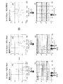
本発明の一実施例である表面処理状況モニタリング装置について、添付図面を参照して説明する。図1は本実施例の表面処理状況モニタリング装置の概略構成、図2は孔深さ測定時(a)と基板厚さ測定時(b)の反射光の状態の模式図である。 A surface treatment status monitoring apparatus according to an embodiment of the present invention will be described with reference to the accompanying drawings. FIG. 1 is a schematic configuration of a surface treatment status monitoring apparatus according to the present embodiment, and FIG.
この表面処理状況モニタリング装置は、例えばプラズマエッチング装置や基板研磨装置などにより加工処理される試料5の基板厚みや形成されるトレンチ深さなど、時々刻々と変化する試料5との間の距離をモニタリングする装置である。該装置は、光源1と、計測光学系2と、分光部3と、データ処理部4とを備える。光源1と計測光学系2、また計測光学系2と分光部3とは光ファイバを介して接続されている。
This surface treatment status monitoring device monitors the distance between the
計測用の光源1としては、例えば中心波長が830nm、半値全幅が15nmであるスーパールミネセントダイオード(SLD)や、同程度の波長幅を有するその他の光源を用いることができる。この光源1から発せられた測定光は入射側光ファイバ21に取り込まれ、ファイバカプラ22を介して光ファイバ23中を進行し、光ファイバ23先端より空間に射出される。光ファイバ23端部から出射された測定光はコリメートレンズ24を介して試料5上に照射される。
As the
試料5の測定対象構造における干渉の状態を図2を用いて説明する。例えば研磨中の基板5Bの厚みを計測する場合には、図2(b)に示すように、基板5B表面からの反射光64、及び基板5B中に進入した光による裏面からの反射光65の2つの反射光による干渉が生ずる。またエッチング中のトレンチ深さを計測する場合には、図2(a)に示すように基板51表面のレジスト層53表面からの反射光62と、レジスト層53中に入り込んだ光に対する基板51表面からの反射光63と、被エッチング部であるトレンチ孔52の底面からの反射光61と、が主として干渉する。これら反射光61〜63又は64〜65はコリメートレンズ24を光照射時とは逆に辿って光ファイバ23に入射する。そして、ファイバカプラ22を経て分光部3に達する。光ファイバ23中を通って分光部3に達するまでに、複数の反射光は十分に干渉し干渉光となる。
The state of interference in the measurement target structure of the
分光部3において干渉光は回折格子31等の分光手段により波長分散され、CCDラインセンサ等のアレイ検出器32により複数波長の光が同時に検出される。アレイ検出器32による各波長に対応した検出信号はデータ処理部4に入力される。データ処理部4は機能ブロックとして、スペクトル記憶部41、差分スペクトル算出部42、フーリエ変換演算部43、光学距離算出部44を含み、後述する処理を実行することで被研磨基板5Bの板厚や被エッチング部であるトレンチ孔52の深さなどが算出される。その算出結果は表示部45により観測者に提示される。
In the
なお、データ処理部4の実体はパーソナルコンピュータであり、該コンピュータに予めインストールされたデータ処理用ソフトウエアを実行することにより、データ処理部4としての機能を発揮させるようにすることができる。
The entity of the
次に、図3〜図5を用いて、本実施例の表面処理状況モニタリング装置に特徴的なデータ処理部4において実行されるデータ処理を中心に説明する。図3は本実施例の表面処理状況モニタリング装置における計測動作を示すフローチャート、図4は各動作のタイミングを示す概略タイミング図、図5はスペクトル取得及びその処理の一例を示す図である。なお、図5の例は、中心波長が800nm、半値全幅(FWHM)が15nmである光源1を用いてトレンチ孔深さを計測したものである。したがって、以下の説明では、エッチングにより形成されるトレンチ孔深さを計測する場合を例示するが、基板や膜層の厚さを計測する場合にもそのまま適用可能である。
Next, with reference to FIG. 3 to FIG. 5, the data processing executed in the
例えばエッチングの開始とともに孔深さの計測が開始されると、データ処理部4は所定時点で分光部3のアレイ検出器32で得られる所定の波長範囲に亘るスペクトルデータを取り込んでスペクトル記憶部41に格納する(ステップS1)。その後、ステップS6において測定終了であると判定されるまで、ステップS1及びS7の処理により、所定時間Δp間隔で繰り返しスペクトルデータを取得する。ここではΔpは後述するΔtの1/3に設定されているが、これに限定されるものではない。
For example, when the measurement of the hole depth is started together with the start of etching, the
ステップS1でスペクトルデータを取得した後、差分スペクトル算出部42はΔtだけ遡った時点のスペクトルデータがスペクトル記憶部41に保存されているか否かを判定し(ステップS2)、保存されていなければ後述する光学距離算出処理を実行できないので上述したステップS7へと進む。図4に示したようにΔp間隔でスペクトルデータの取得・保存を繰り返してゆくと、ある時点においてステップS2の判定はYesとなる。いま、時刻t0においてスペクトルデータP1が取得され、時刻t0からΔt経過後の時刻t1においてスペクトルデータP4が取得されたものとする。時刻t1において得られる観測スペクトル(図5(c))は、干渉を含まない反射光スペクトル(ベーススペクトル)(図5(a))に、測定対象であるトレンチ孔52に起因して生じた干渉によるスペクトル干渉縞(図5(b))が重畳されたものである。
After acquiring the spectrum data in step S1, the difference
従来一般的には、この観測スペクトルを例えばフーリエ変換(FT)演算で周波数解析することによってフーリエ変換後信号(図5(d))を求め、その信号上のピーク位置を求めることによって干渉を引き起こした光路長を推定する。図5(c)はd=20.3μmの光路長を計測して得られるスペクトルであるが、これに対するフーリエ変換後信号である図5(d)が示すとおり、d=20.3μmの位置に信号は存在するものの、距離0μmの側に現れるバイアス信号に解析対象とする信号が隠れてしまい、ピーク位置(矢印箇所)の推定が困難となっている。本来は図5(c)に示した観測スペクトルから干渉に寄与しないスペクトルであるベーススペクトル(図5(a))を予め差し引いてフーリエ変換を行うことが望ましい。しかしながら、前述したとおりベーススペクトルの形状は測定光学系の様々な歪みや試料の反射率などの影響を受けるため、測定毎にベーススペクトルの適切な形状・大きさを推定することは非常に困難である。その結果、観測スペクトルから適切にペーススペクトルを差し引くことができず、フーリエ変換後信号から十分な精度でピーク位置を見つけるのが難しくなる。 Conventionally, this observed spectrum is subjected to frequency analysis by, for example, Fourier transform (FT) calculation to obtain a signal after Fourier transform (FIG. 5 (d)), and interference is caused by obtaining a peak position on the signal. Estimate the optical path length. FIG. 5 (c) shows a spectrum obtained by measuring the optical path length of d = 20.3 μm. As shown in FIG. 5 (d) which is a signal after Fourier transform, d = 20.3 μm. Although the signal exists, the signal to be analyzed is hidden behind the bias signal that appears on the distance of 0 μm, making it difficult to estimate the peak position (arrow location). Originally, it is desirable to perform Fourier transform by subtracting in advance the base spectrum (FIG. 5A), which is a spectrum that does not contribute to interference, from the observed spectrum shown in FIG. However, as described above, since the shape of the base spectrum is affected by various distortions of the measurement optical system and the reflectance of the sample, it is very difficult to estimate the appropriate shape and size of the base spectrum for each measurement. is there. As a result, the pace spectrum cannot be appropriately subtracted from the observed spectrum, and it becomes difficult to find the peak position with sufficient accuracy from the signal after Fourier transform.
これに対し、本実施例で採用している手法では、ベーススペクトルではなく一定時間だけ遡った時点の干渉波形を参照波形として用いる。ここでは、時刻t1からΔtだけ遡った時刻t0において取得された観測スペクトルP1がスペクトル記憶部41に格納されているから、それを参照波形として利用する。このΔtは測定対象構造の光学距離変化Δdが測定光の波長を超えない程度の時間以内に定められている。いま、時刻t0において取得された観測スペクトルは図5(g)(図5(g)はエッチングが200nm進行する前の孔深さd=20.1μmの例)である。この観測スペクトルも、図5(e)に示した干渉を含まない反射光スペクトル(ベーススペクトル)に、測定対象であるトレンチ孔52に起因して生じた干渉によるスペクトル干渉縞(図5(f))が重畳されたものである。
On the other hand, in the method employed in the present embodiment, an interference waveform that is not a base spectrum but is traced back for a fixed time is used as a reference waveform. Here, since the observed spectrum P1 acquired at time t0 that is back by Δt from time t1 is stored in the
時刻t1と時刻t0との時間差Δtが十分に短い場合には、ベーススペクトルの変動は無視できる程度である。そこで、差分スペクトル算出部42は時刻t1におけるスペクトルデータP4から時刻t0におけるスペクトルデータP1を差し引く演算を行う(ステップS3)。この演算により、ほぼ同じであるベーススペクトルはキャンセルされ、実効的に同じ周波数で位相が異なる2つの干渉縞(図5(b)、(f))のみの除算と等価となり、やはり同じ周波数である干渉縞(図5(i))を差分スペクトルとして得ることができる。この差分スペクトルはベーススペクトルを含まない実質的に正規化された干渉スペクトルである。そこで、フーリエ変換演算部43は上記差分スペクトルに対しフーリエ変換による周波数解析を行うことによって図5(j)に示すようなフーリエ変換後信号を求める(ステップS4)。
When the time difference Δt between the time t1 and the time t0 is sufficiently short, the fluctuation of the base spectrum is negligible. Therefore, the difference
このフーリエ変換後信号は図5(d)に示した信号とは異なりバイアス信号を含まないため、ピークが明瞭に現れ、ピーク位置の推定が容易となる。光学距離算出部44は差分スペクトルから得られたフーリエ変換後信号上でピーク位置を確定させることにより、干渉を引き起こした光路長を求める。そして、その光路長から測定対象であるトレンチ孔深さや基板厚さを求めて表示部45から出力する(ステップS5)。図5(j)の例では、ピーク位置から光路長差が20μmであると求まる。
Unlike the signal shown in FIG. 5D, this Fourier-transformed signal does not include a bias signal, so that a peak appears clearly and peak position can be easily estimated. The optical
そうして孔深さが求まったならば、ステップS6へと進み、上述したように測定終了でなければステップS7へと進んで、エッチングの進行に伴って変化する新たなスペクトルの取得を実行する。新たなスペクトルを取得する毎にΔtだけ遡った時点のスペクトルとの差分スペクトルを求め(図4参照)、この差分スペクトルからトレンチ孔深さに対応した光路長が算出される。したがって、新たなスペクトルを取得する毎に、その時点で最新のトレンチ孔深さを計算して表示部45から出力することができる。
If the hole depth is found, the process proceeds to step S6. If the measurement is not completed as described above, the process proceeds to step S7, and acquisition of a new spectrum that changes with the progress of etching is executed. . Every time a new spectrum is acquired, a difference spectrum from the spectrum traced back by Δt is obtained (see FIG. 4), and the optical path length corresponding to the trench hole depth is calculated from this difference spectrum. Therefore, every time a new spectrum is acquired, the latest trench hole depth can be calculated and output from the
上述したように差分スペクトルを計算する2つのスペクトルの時間差Δtは、測定対象構造に対する光学距離変化Δdが測定光の1波長を超えない程度の時間以内に定める必要がある。これは予め定めておいてもよいが、エッチング(又は研磨等)速度が不明である場合などには適切な値を決めるのが難しいし、またその値が適切でないと、干渉縞を示す差分スペクトルの波形が小さくなるおそれもある。そこで、Δtを予め決めておくのではなく、取得した差分スペクトルから適応的にΔtを決めるようにしてもよい。 As described above, the time difference Δt between the two spectra for calculating the difference spectrum needs to be determined within a time such that the optical distance change Δd with respect to the measurement target structure does not exceed one wavelength of the measurement light. This may be determined in advance, but it is difficult to determine an appropriate value when the etching (or polishing) speed is unknown, and if the value is not appropriate, a differential spectrum indicating interference fringes. There is also a possibility that the waveform of will be small. Therefore, Δt may not be determined in advance, but may be determined adaptively from the acquired difference spectrum.
例えば上記例の場合、観測スペクトルP6に対し参照波形としてP3以外にP4、P5(さらに場合によってはP2以前のスペクトル)を選択し得るが、例えばP6−P5、P6−P4、P6−P3の3つの組み合わせについてそれぞれ差分スペクトルを計算し、得られた差分スペクトルの振幅の大きさを比較して最も適切な組み合わせを選択して、その差分スペクトルを周波数解析するとよい。また、単に差分スペクトルに現れる波形(干渉縞)の振幅の大きさを判断するのではなく、差分スペクトルに現れる波形のカーブで囲まれる面積の大きさ又はその変化振幅に基づいて最適な組み合わせを選択するようにしてもよい。なお、エッチング(又は研磨等)速度が一定である場合には、そのプロセスの途中で最適なΔtが変わることはないため、上記のような処理によって一旦適切なΔtを定めたならばそのプロセス実行中は同じΔtを用いて差分スペクトルを計算するようにすればよい。
For example, in the case of the above example, P4 and P5 (in addition to the spectrum before P2 depending on the case) other than P3 can be selected as the reference waveform for the observed spectrum P6. For example, P6-P5, P6-P4, P6-
また上記実施例では、差分スペクトルに対してフーリエ変換による周波数解析を実施することで求めたフーリエ変換後信号から干渉により生じる光路長を算出していたが、近年、周波数解析を行うためにフーリエ変換に代わる方法としてよく用いられる最大エントロピー法(MEM)による周波数解析を実施してもよい。 In the above embodiment, the optical path length caused by the interference is calculated from the post-Fourier-transformed signal obtained by performing frequency analysis by Fourier transform on the difference spectrum, but in recent years, Fourier transform has been performed to perform frequency analysis. Alternatively, frequency analysis by the maximum entropy method (MEM), which is often used as an alternative method, may be performed.
また、周波数解析ではなく、上記(8)式に基づいた位相検出を行う手法について説明する。図5(j)に示したようなフーリエ変換後信号では、光路長dに対応する信号の拡がりが光源1のスペクトル幅15nmの逆数である20μm程度の幅をもつ。フーリエ変換の代わりに最大エントロピー法による周波数解析を行うことで、より幅の狭い周波数信号を推定することも可能であるが、いずれにせよ周波数解析では0.1μm以下の精度で周波数推定を行うことは困難である。そこで、図5(i)の差分スペクトルの位相に着目すると、そのゼロクロス点(干渉振幅がゼロとなる波長)はλ=800nmであることから、(8)式においておおよそd=20.3μmとなるよう定数k=101±1と設定すると、Δd=0.2μm、ゼロクロスλ=0.8μm、λc=0.8μmであるから、測定光路長dはd=20.10μm(k=100)、d=20.30μ(k=101)、d=20.50μm(k=102)のいずれかであり、決してd=20.25μmやd=20.35μmではないことが判明する。このようにして、差分スペクトル(干渉縞)の位相検出を行うことにより、周波数解析を行うよりも高い分解能で以て光学距離を算出することができる。
Also, a method for performing phase detection based on the above equation (8) instead of frequency analysis will be described. In the post-Fourier-transformed signal as shown in FIG. 5 (j), the signal spread corresponding to the optical path length d has a width of about 20 μm which is the reciprocal of the spectral width 15 nm of the
続いて、基板研磨中の基板厚みのモニタリングにおいて、上記説明した本発明による手法を用いることで、測定対象以外の構造による干渉縞をキャンセルした結果の一例を図6により説明する。図6は、測定経路内に18μm厚のSiO2層を含む10μmの厚さのSiを計測した場合のシミュレーション結果である。Siの厚みを測定するため、Siの吸収のない波長帯である1300nmの光源を用いた。図6(a)は研磨が10μmまで進行した際に取得されるスペクトルであるが、10μmのSiによる光路長35μmに対して18μmのSiO2層の光路長は27μmであり、非常に近接している。そのため、フーリエ変換後の信号位置が近く分離が困難であり、図6(b)に示すとおり、一般的なフーリエ解析ではSiの板厚を示すピーク位置の推定が非常に困難である。 Next, an example of a result of canceling interference fringes due to a structure other than the measurement target by using the above-described method according to the present invention in monitoring the substrate thickness during substrate polishing will be described with reference to FIG. FIG. 6 shows a simulation result when Si having a thickness of 10 μm including an SiO 2 layer having a thickness of 18 μm in the measurement path is measured. In order to measure the thickness of Si, a light source having a wavelength of 1300 nm, which is a wavelength band without absorption of Si, was used. FIG. 6A shows a spectrum acquired when polishing proceeds to 10 μm, whereas the optical path length of the 18 μm SiO 2 layer is 27 μm, which is very close to the optical path length of 35 μm with 10 μm Si. Yes. For this reason, the signal position after Fourier transform is close and difficult to separate, and as shown in FIG. 6B, it is very difficult to estimate the peak position indicating the thickness of Si by general Fourier analysis.
このような場合でも、一定時間だけ遡った時点における研磨状態である10.02μm厚Siの際に取得された図6(c)に示すスペクトルを用いて差分処理を行いさえすれば、SiO2層による干渉縞が存在しない図6(e)に示す正規化スペクトルを生成することができる。その後は上記例と同様にこのスペクトルをフーリエ変換することにより、図6(f)に示すようなSi層のみに由来するフーリエ変換後信号が得られるから、容易にピーク位置を求め、これからSi板厚を算出することができる。 Even in such a case, as long as the difference processing is performed using the spectrum shown in FIG. 6C acquired in the case of Si having a thickness of 10.02 μm, which is a polished state at a certain time, the SiO 2 layer The normalized spectrum shown in FIG. 6E without the interference fringes can be generated. Thereafter, the spectrum is Fourier-transformed in the same manner as in the above example to obtain a post-Fourier-transformed signal derived only from the Si layer as shown in FIG. 6 (f). The thickness can be calculated.
なお、上記実施例はいずれも本発明の一例にすぎず、本発明の趣旨の範囲で適宜修正、追加、変更を加えても本願特許請求の範囲に包含されることは明らかである。 The above-described embodiments are merely examples of the present invention, and it is obvious that modifications, additions, and changes as appropriate within the scope of the present invention are included in the scope of the claims of the present application.
1…光源
2…計測光学系
21…入射側光ファイバ
22…ファイバカプラ
23…光ファイバ
24…コリメートレンズ
3…分光部
31…回折格子
32…アレイ検出器
4…データ処理部
41…スペクトル記憶部
42…差分スペクトル算出部
43…フーリエ変換演算部
44…光学距離算出部
5…ステップS
5…試料
5A、5B、51…基板
52…トレンチ孔
53…レジスト層
61〜65…反射光
DESCRIPTION OF
5 ...
Claims (6)
a)微小な時間だけ隔てた2つの時点で前記検出手段によりそれぞれ所定波長範囲のスペクトルを取得するスペクトル取得手段と、
b)前記スペクトル取得手段による2つのスペクトルの差分スペクトルを求める差分スペクトル算出手段と、
c)前記差分スペクトルに対し周波数解析を行って目的とする干渉距離を算出し、該干渉距離から測定対象構造のサイズを求める周波数解析手段と、
を備えることを特徴とする表面処理状況モニタリング装置。 A surface treatment status monitoring device for measuring the size of a structure to be measured such as the depth or step of a hole or groove formed on a substrate by surface treatment, or the thickness or thickness of a film layer or substrate that increases or decreases. A light source that generates measurement light having a wavelength width, an interference optical system that interferes with light reflected from the first part and the second part of the measurement target structure, and a spectral unit that wavelength-disperses interference light from the interference optical system And a surface treatment status monitoring apparatus comprising: a detection unit that detects, for each wavelength, the light wavelength-dispersed by the spectroscopic unit.
a) a spectrum acquisition means for acquiring a spectrum in a predetermined wavelength range by the detection means at two time points separated by a minute time;
b) a difference spectrum calculation means for obtaining a difference spectrum of two spectra by the spectrum acquisition means;
c) calculating a target interference distance by performing frequency analysis on the difference spectrum, and determining a size of the structure to be measured from the interference distance;
A surface treatment status monitoring device comprising:
前記周波数解析手段による周波数解析はフーリエ変換演算であることを特徴とする表面処理状況モニタリング装置。 The surface treatment status monitoring device according to claim 1,
The surface treatment status monitoring apparatus, wherein the frequency analysis by the frequency analysis means is a Fourier transform operation.
前記周波数解析手段による周波数解析は最大エントロピー法による解析であることを特徴とする表面処理状況モニタリング装置。 The surface treatment status monitoring device according to claim 1,
The surface treatment status monitoring apparatus, wherein the frequency analysis by the frequency analysis means is analysis by a maximum entropy method.
a)微小な時間だけ隔てた2つの時点で前記検出手段によりそれぞれ所定波長範囲のスペクトルを取得するスペクトル取得手段と、
b)前記スペクトル取得手段による2つのスペクトルの差分スペクトルを求める差分スペクトル算出手段と、
c)前記差分スペクトルに基づいて位相を検出し、該位相から目的とする干渉距離を算出し、該干渉距離から測定対象構造のサイズを求める周波数解析手段と、
を備えることを特徴とする表面処理状況モニタリング装置。 A surface treatment status monitoring device for measuring the size of a structure to be measured such as the depth or step of a hole or groove formed on a substrate by surface treatment, or the thickness or thickness of a film layer or substrate that increases or decreases. A light source that generates measurement light having a wavelength width, an interference optical system that interferes with light reflected from the first part and the second part of the measurement target structure, and a spectral unit that wavelength-disperses interference light from the interference optical system And a surface treatment status monitoring apparatus comprising: a detection unit that detects, for each wavelength, the light wavelength-dispersed by the spectroscopic unit.
a) a spectrum acquisition means for acquiring a spectrum in a predetermined wavelength range by the detection means at two time points separated by a minute time;
b) a difference spectrum calculation means for obtaining a difference spectrum of two spectra by the spectrum acquisition means;
c) detecting a phase based on the difference spectrum, calculating a target interference distance from the phase, and calculating a size of the structure to be measured from the interference distance;
A surface treatment status monitoring device comprising:
前記差分スペクトルの振幅の大きさに基づいて前記微小な時間の最適値を判別して設定する取得条件決定手段をさらに備えることを特徴とする表面処理状況モニタリング装置。 The surface treatment status monitoring device according to any one of claims 1 to 4,
The surface treatment status monitoring apparatus further comprising an acquisition condition determining means for determining and setting the optimum value of the minute time based on the amplitude of the difference spectrum.
前記差分スペクトルのカーブで囲まれる面積の大きさ又はその変化振幅に基づいて前記微小な時間の最適値を判別して設定する取得条件決定手段をさらに備えることを特徴とする表面処理状況モニタリング装置。 The surface treatment status monitoring device according to any one of claims 1 to 4,
The surface treatment status monitoring device further comprising an acquisition condition determining means for determining and setting the optimum value of the minute time based on the size of the area surrounded by the curve of the difference spectrum or the change amplitude thereof.
Priority Applications (2)
| Application Number | Priority Date | Filing Date | Title |
|---|---|---|---|
| JP2011266613A JP2013120063A (en) | 2011-12-06 | 2011-12-06 | Surface treatment condition monitoring apparatus |
| US13/707,407 US20130169958A1 (en) | 2011-12-06 | 2012-12-06 | Surface Processing Progress Monitoring System |
Applications Claiming Priority (1)
| Application Number | Priority Date | Filing Date | Title |
|---|---|---|---|
| JP2011266613A JP2013120063A (en) | 2011-12-06 | 2011-12-06 | Surface treatment condition monitoring apparatus |
Publications (2)
| Publication Number | Publication Date |
|---|---|
| JP2013120063A true JP2013120063A (en) | 2013-06-17 |
| JP2013120063A5 JP2013120063A5 (en) | 2014-05-08 |
Family
ID=48694578
Family Applications (1)
| Application Number | Title | Priority Date | Filing Date |
|---|---|---|---|
| JP2011266613A Pending JP2013120063A (en) | 2011-12-06 | 2011-12-06 | Surface treatment condition monitoring apparatus |
Country Status (2)
| Country | Link |
|---|---|
| US (1) | US20130169958A1 (en) |
| JP (1) | JP2013120063A (en) |
Cited By (1)
| Publication number | Priority date | Publication date | Assignee | Title |
|---|---|---|---|---|
| JP2017078632A (en) * | 2015-10-20 | 2017-04-27 | 国立大学法人 和歌山大学 | Observation method of tomographic structure, observation device, and computer program |
Families Citing this family (4)
| Publication number | Priority date | Publication date | Assignee | Title |
|---|---|---|---|---|
| US20150022658A1 (en) | 2013-07-16 | 2015-01-22 | University Of North Carolina At Charlotte | Noise reduction techniques, fractional bi-spectrum and fractional cross-correlation, and applications |
| KR102313350B1 (en) | 2014-09-02 | 2021-10-15 | 삼성전자주식회사 | Optical measuring methods and apparatus |
| KR20180064791A (en) * | 2016-12-06 | 2018-06-15 | 삼성전자주식회사 | Polishing method and polishing apparatus |
| CN108515460A (en) * | 2018-04-10 | 2018-09-11 | 湖南工学院 | Planar optical elements sub-surface damage detection method |
Citations (9)
| Publication number | Priority date | Publication date | Assignee | Title |
|---|---|---|---|---|
| JPH11274259A (en) * | 1998-03-26 | 1999-10-08 | Hitachi Ltd | Thickness measuring device and thickness controller |
| JP2002081917A (en) * | 2000-06-20 | 2002-03-22 | Hitachi Ltd | Film thickness measuring method and device for processed material by light emission spectroscopy, and processing method and device for processed material using the same |
| JP2004507070A (en) * | 1999-09-30 | 2004-03-04 | ラム リサーチ コーポレーション | Method and apparatus for in-situ monitoring of plasma etching and deposition processes using a pulsed broadband light source |
| JP2004253516A (en) * | 2003-02-19 | 2004-09-09 | Hitachi High-Technologies Corp | Dry etching method and apparatus for test sample |
| JP2005184013A (en) * | 2001-03-12 | 2005-07-07 | Denso Corp | Method for measuring film thickness of semiconductor layer and method for manufacturing semiconductor substrate |
| JP2008142443A (en) * | 2006-12-13 | 2008-06-26 | Fujifilm Corp | Optical tomographic apparatus |
| JP2008218898A (en) * | 2007-03-07 | 2008-09-18 | Hitachi High-Technologies Corp | Plasma processing device |
| WO2011045967A1 (en) * | 2009-10-13 | 2011-04-21 | 浜松ホトニクス株式会社 | Film thickness measurement device and film thickness measurement method |
| US20110216328A1 (en) * | 2010-03-02 | 2011-09-08 | Yoichi Kobayashi | Polishing monitoring method, polishing method, and polishing monitoring apparatus |
Family Cites Families (5)
| Publication number | Priority date | Publication date | Assignee | Title |
|---|---|---|---|---|
| JP3946470B2 (en) * | 2001-03-12 | 2007-07-18 | 株式会社デンソー | Method for measuring thickness of semiconductor layer and method for manufacturing semiconductor substrate |
| WO2004088241A2 (en) * | 2003-03-26 | 2004-10-14 | Southwest Sciences Incorporated | Method and apparatus for imaging internal structures of transparent and translucent materials |
| JP5862433B2 (en) * | 2012-04-09 | 2016-02-16 | 株式会社島津製作所 | Surface treatment status monitoring device |
| JP5888111B2 (en) * | 2012-05-18 | 2016-03-16 | 株式会社島津製作所 | Etching monitor device |
| JP2014002068A (en) * | 2012-06-19 | 2014-01-09 | Shimadzu Corp | Thickness monitoring device, etching depth monitoring device, and thickness monitoring method |
-
2011
- 2011-12-06 JP JP2011266613A patent/JP2013120063A/en active Pending
-
2012
- 2012-12-06 US US13/707,407 patent/US20130169958A1/en not_active Abandoned
Patent Citations (9)
| Publication number | Priority date | Publication date | Assignee | Title |
|---|---|---|---|---|
| JPH11274259A (en) * | 1998-03-26 | 1999-10-08 | Hitachi Ltd | Thickness measuring device and thickness controller |
| JP2004507070A (en) * | 1999-09-30 | 2004-03-04 | ラム リサーチ コーポレーション | Method and apparatus for in-situ monitoring of plasma etching and deposition processes using a pulsed broadband light source |
| JP2002081917A (en) * | 2000-06-20 | 2002-03-22 | Hitachi Ltd | Film thickness measuring method and device for processed material by light emission spectroscopy, and processing method and device for processed material using the same |
| JP2005184013A (en) * | 2001-03-12 | 2005-07-07 | Denso Corp | Method for measuring film thickness of semiconductor layer and method for manufacturing semiconductor substrate |
| JP2004253516A (en) * | 2003-02-19 | 2004-09-09 | Hitachi High-Technologies Corp | Dry etching method and apparatus for test sample |
| JP2008142443A (en) * | 2006-12-13 | 2008-06-26 | Fujifilm Corp | Optical tomographic apparatus |
| JP2008218898A (en) * | 2007-03-07 | 2008-09-18 | Hitachi High-Technologies Corp | Plasma processing device |
| WO2011045967A1 (en) * | 2009-10-13 | 2011-04-21 | 浜松ホトニクス株式会社 | Film thickness measurement device and film thickness measurement method |
| US20110216328A1 (en) * | 2010-03-02 | 2011-09-08 | Yoichi Kobayashi | Polishing monitoring method, polishing method, and polishing monitoring apparatus |
Cited By (1)
| Publication number | Priority date | Publication date | Assignee | Title |
|---|---|---|---|---|
| JP2017078632A (en) * | 2015-10-20 | 2017-04-27 | 国立大学法人 和歌山大学 | Observation method of tomographic structure, observation device, and computer program |
Also Published As
| Publication number | Publication date |
|---|---|
| US20130169958A1 (en) | 2013-07-04 |
Similar Documents
| Publication | Publication Date | Title |
|---|---|---|
| JP5862433B2 (en) | Surface treatment status monitoring device | |
| TWI465682B (en) | Film thickness measuring device and measuring method | |
| US8885173B2 (en) | Film thickness measurement device and film thickness measurement method | |
| KR102330413B1 (en) | Temperature measuring method, substrate processing system and component to be provided in substrate processing apparatus of the substrate processing system | |
| JP2013195290A (en) | Optical distance measurement device | |
| US10203195B2 (en) | Noise reduction techniques, fractional bi-spectrum and fractional cross-correlation, and applications | |
| TW201728869A (en) | Device and method for measuring height in the presence of thin layers | |
| JP2013120063A (en) | Surface treatment condition monitoring apparatus | |
| WO2012077652A1 (en) | Etching monitoring apparatus | |
| JP2018084434A (en) | Measurement device and measurement method | |
| US9228828B2 (en) | Thickness monitoring device, etching depth monitoring device and thickness monitoring method | |
| US9305753B2 (en) | Thickness change monitor wafer for in situ film thickness monitoring | |
| JP2013152191A (en) | Multi-wavelength interferometer | |
| JP2013120063A5 (en) | ||
| JP2016080668A (en) | Device and method for monitoring surface treatment state | |
| KR20170066375A (en) | Method and system for inspecting transparent wafers for electronics, optics or optoelectronics | |
| JP5888111B2 (en) | Etching monitor device | |
| JP2005084019A (en) | Temperature measuring method of substrate | |
| JP2015105850A (en) | Refractive index measurement method, refractive index measurement device, and method for manufacturing optical element | |
| JP2013048183A (en) | Etching monitoring device | |
| TW201502492A (en) | Method and apparatus for measuring refractive index and method for manufacturing optical element | |
| JP2018004409A (en) | Refractive index measurement method, refractive index measurement device, and method of manufacturing optical element | |
| JPS6385305A (en) | Apparatus for measuring depth of fine groove | |
| JP6544171B2 (en) | Surface treatment status monitoring device | |
| JP2015137909A (en) | Etching monitor device |
Legal Events
| Date | Code | Title | Description |
|---|---|---|---|
| A521 | Request for written amendment filed |
Free format text: JAPANESE INTERMEDIATE CODE: A523 Effective date: 20140325 |
|
| A621 | Written request for application examination |
Free format text: JAPANESE INTERMEDIATE CODE: A621 Effective date: 20140325 |
|
| A977 | Report on retrieval |
Free format text: JAPANESE INTERMEDIATE CODE: A971007 Effective date: 20141216 |
|
| A131 | Notification of reasons for refusal |
Free format text: JAPANESE INTERMEDIATE CODE: A131 Effective date: 20141224 |
|
| A02 | Decision of refusal |
Free format text: JAPANESE INTERMEDIATE CODE: A02 Effective date: 20150414 |