JP2012532453A - White light electroluminescent device with adjustable color temperature - Google Patents
White light electroluminescent device with adjustable color temperature Download PDFInfo
- Publication number
- JP2012532453A JP2012532453A JP2012517777A JP2012517777A JP2012532453A JP 2012532453 A JP2012532453 A JP 2012532453A JP 2012517777 A JP2012517777 A JP 2012517777A JP 2012517777 A JP2012517777 A JP 2012517777A JP 2012532453 A JP2012532453 A JP 2012532453A
- Authority
- JP
- Japan
- Prior art keywords
- light
- color
- light emitting
- color temperature
- line segment
- Prior art date
- Legal status (The legal status is an assumption and is not a legal conclusion. Google has not performed a legal analysis and makes no representation as to the accuracy of the status listed.)
- Pending
Links
Images


Classifications
-
- H—ELECTRICITY
- H01—ELECTRIC ELEMENTS
- H01L—SEMICONDUCTOR DEVICES NOT COVERED BY CLASS H10
- H01L33/00—Semiconductor devices with at least one potential-jump barrier or surface barrier specially adapted for light emission; Processes or apparatus specially adapted for the manufacture or treatment thereof or of parts thereof; Details thereof
- H01L33/48—Semiconductor devices with at least one potential-jump barrier or surface barrier specially adapted for light emission; Processes or apparatus specially adapted for the manufacture or treatment thereof or of parts thereof; Details thereof characterised by the semiconductor body packages
- H01L33/50—Wavelength conversion elements
- H01L33/501—Wavelength conversion elements characterised by the materials, e.g. binder
- H01L33/502—Wavelength conversion materials
- H01L33/504—Elements with two or more wavelength conversion materials
-
- H—ELECTRICITY
- H01—ELECTRIC ELEMENTS
- H01L—SEMICONDUCTOR DEVICES NOT COVERED BY CLASS H10
- H01L33/00—Semiconductor devices with at least one potential-jump barrier or surface barrier specially adapted for light emission; Processes or apparatus specially adapted for the manufacture or treatment thereof or of parts thereof; Details thereof
- H01L33/36—Semiconductor devices with at least one potential-jump barrier or surface barrier specially adapted for light emission; Processes or apparatus specially adapted for the manufacture or treatment thereof or of parts thereof; Details thereof characterised by the electrodes
- H01L33/38—Semiconductor devices with at least one potential-jump barrier or surface barrier specially adapted for light emission; Processes or apparatus specially adapted for the manufacture or treatment thereof or of parts thereof; Details thereof characterised by the electrodes with a particular shape
-
- H—ELECTRICITY
- H05—ELECTRIC TECHNIQUES NOT OTHERWISE PROVIDED FOR
- H05B—ELECTRIC HEATING; ELECTRIC LIGHT SOURCES NOT OTHERWISE PROVIDED FOR; CIRCUIT ARRANGEMENTS FOR ELECTRIC LIGHT SOURCES, IN GENERAL
- H05B45/00—Circuit arrangements for operating light-emitting diodes [LED]
- H05B45/20—Controlling the colour of the light
-
- H—ELECTRICITY
- H05—ELECTRIC TECHNIQUES NOT OTHERWISE PROVIDED FOR
- H05B—ELECTRIC HEATING; ELECTRIC LIGHT SOURCES NOT OTHERWISE PROVIDED FOR; CIRCUIT ARRANGEMENTS FOR ELECTRIC LIGHT SOURCES, IN GENERAL
- H05B45/00—Circuit arrangements for operating light-emitting diodes [LED]
- H05B45/40—Details of LED load circuits
-
- H—ELECTRICITY
- H01—ELECTRIC ELEMENTS
- H01L—SEMICONDUCTOR DEVICES NOT COVERED BY CLASS H10
- H01L2224/00—Indexing scheme for arrangements for connecting or disconnecting semiconductor or solid-state bodies and methods related thereto as covered by H01L24/00
- H01L2224/01—Means for bonding being attached to, or being formed on, the surface to be connected, e.g. chip-to-package, die-attach, "first-level" interconnects; Manufacturing methods related thereto
- H01L2224/42—Wire connectors; Manufacturing methods related thereto
- H01L2224/44—Structure, shape, material or disposition of the wire connectors prior to the connecting process
- H01L2224/45—Structure, shape, material or disposition of the wire connectors prior to the connecting process of an individual wire connector
- H01L2224/45001—Core members of the connector
- H01L2224/45099—Material
- H01L2224/451—Material with a principal constituent of the material being a metal or a metalloid, e.g. boron (B), silicon (Si), germanium (Ge), arsenic (As), antimony (Sb), tellurium (Te) and polonium (Po), and alloys thereof
- H01L2224/45138—Material with a principal constituent of the material being a metal or a metalloid, e.g. boron (B), silicon (Si), germanium (Ge), arsenic (As), antimony (Sb), tellurium (Te) and polonium (Po), and alloys thereof the principal constituent melting at a temperature of greater than or equal to 950°C and less than 1550°C
- H01L2224/45139—Silver (Ag) as principal constituent
-
- H—ELECTRICITY
- H01—ELECTRIC ELEMENTS
- H01L—SEMICONDUCTOR DEVICES NOT COVERED BY CLASS H10
- H01L2224/00—Indexing scheme for arrangements for connecting or disconnecting semiconductor or solid-state bodies and methods related thereto as covered by H01L24/00
- H01L2224/01—Means for bonding being attached to, or being formed on, the surface to be connected, e.g. chip-to-package, die-attach, "first-level" interconnects; Manufacturing methods related thereto
- H01L2224/42—Wire connectors; Manufacturing methods related thereto
- H01L2224/47—Structure, shape, material or disposition of the wire connectors after the connecting process
- H01L2224/48—Structure, shape, material or disposition of the wire connectors after the connecting process of an individual wire connector
- H01L2224/4805—Shape
- H01L2224/4809—Loop shape
- H01L2224/48091—Arched
-
- H—ELECTRICITY
- H01—ELECTRIC ELEMENTS
- H01L—SEMICONDUCTOR DEVICES NOT COVERED BY CLASS H10
- H01L2224/00—Indexing scheme for arrangements for connecting or disconnecting semiconductor or solid-state bodies and methods related thereto as covered by H01L24/00
- H01L2224/01—Means for bonding being attached to, or being formed on, the surface to be connected, e.g. chip-to-package, die-attach, "first-level" interconnects; Manufacturing methods related thereto
- H01L2224/42—Wire connectors; Manufacturing methods related thereto
- H01L2224/47—Structure, shape, material or disposition of the wire connectors after the connecting process
- H01L2224/48—Structure, shape, material or disposition of the wire connectors after the connecting process of an individual wire connector
- H01L2224/484—Connecting portions
- H01L2224/48463—Connecting portions the connecting portion on the bonding area of the semiconductor or solid-state body being a ball bond
- H01L2224/48465—Connecting portions the connecting portion on the bonding area of the semiconductor or solid-state body being a ball bond the other connecting portion not on the bonding area being a wedge bond, i.e. ball-to-wedge, regular stitch
-
- H—ELECTRICITY
- H01—ELECTRIC ELEMENTS
- H01L—SEMICONDUCTOR DEVICES NOT COVERED BY CLASS H10
- H01L25/00—Assemblies consisting of a plurality of individual semiconductor or other solid state devices ; Multistep manufacturing processes thereof
- H01L25/03—Assemblies consisting of a plurality of individual semiconductor or other solid state devices ; Multistep manufacturing processes thereof all the devices being of a type provided for in the same subgroup of groups H01L27/00 - H01L33/00, or in a single subclass of H10K, H10N, e.g. assemblies of rectifier diodes
- H01L25/04—Assemblies consisting of a plurality of individual semiconductor or other solid state devices ; Multistep manufacturing processes thereof all the devices being of a type provided for in the same subgroup of groups H01L27/00 - H01L33/00, or in a single subclass of H10K, H10N, e.g. assemblies of rectifier diodes the devices not having separate containers
- H01L25/075—Assemblies consisting of a plurality of individual semiconductor or other solid state devices ; Multistep manufacturing processes thereof all the devices being of a type provided for in the same subgroup of groups H01L27/00 - H01L33/00, or in a single subclass of H10K, H10N, e.g. assemblies of rectifier diodes the devices not having separate containers the devices being of a type provided for in group H01L33/00
- H01L25/0753—Assemblies consisting of a plurality of individual semiconductor or other solid state devices ; Multistep manufacturing processes thereof all the devices being of a type provided for in the same subgroup of groups H01L27/00 - H01L33/00, or in a single subclass of H10K, H10N, e.g. assemblies of rectifier diodes the devices not having separate containers the devices being of a type provided for in group H01L33/00 the devices being arranged next to each other
-
- H—ELECTRICITY
- H01—ELECTRIC ELEMENTS
- H01L—SEMICONDUCTOR DEVICES NOT COVERED BY CLASS H10
- H01L2924/00—Indexing scheme for arrangements or methods for connecting or disconnecting semiconductor or solid-state bodies as covered by H01L24/00
- H01L2924/0001—Technical content checked by a classifier
- H01L2924/00014—Technical content checked by a classifier the subject-matter covered by the group, the symbol of which is combined with the symbol of this group, being disclosed without further technical details
-
- H—ELECTRICITY
- H01—ELECTRIC ELEMENTS
- H01L—SEMICONDUCTOR DEVICES NOT COVERED BY CLASS H10
- H01L33/00—Semiconductor devices with at least one potential-jump barrier or surface barrier specially adapted for light emission; Processes or apparatus specially adapted for the manufacture or treatment thereof or of parts thereof; Details thereof
- H01L33/02—Semiconductor devices with at least one potential-jump barrier or surface barrier specially adapted for light emission; Processes or apparatus specially adapted for the manufacture or treatment thereof or of parts thereof; Details thereof characterised by the semiconductor bodies
- H01L33/08—Semiconductor devices with at least one potential-jump barrier or surface barrier specially adapted for light emission; Processes or apparatus specially adapted for the manufacture or treatment thereof or of parts thereof; Details thereof characterised by the semiconductor bodies with a plurality of light emitting regions, e.g. laterally discontinuous light emitting layer or photoluminescent region integrated within the semiconductor body
-
- H—ELECTRICITY
- H01—ELECTRIC ELEMENTS
- H01L—SEMICONDUCTOR DEVICES NOT COVERED BY CLASS H10
- H01L33/00—Semiconductor devices with at least one potential-jump barrier or surface barrier specially adapted for light emission; Processes or apparatus specially adapted for the manufacture or treatment thereof or of parts thereof; Details thereof
- H01L33/02—Semiconductor devices with at least one potential-jump barrier or surface barrier specially adapted for light emission; Processes or apparatus specially adapted for the manufacture or treatment thereof or of parts thereof; Details thereof characterised by the semiconductor bodies
- H01L33/20—Semiconductor devices with at least one potential-jump barrier or surface barrier specially adapted for light emission; Processes or apparatus specially adapted for the manufacture or treatment thereof or of parts thereof; Details thereof characterised by the semiconductor bodies with a particular shape, e.g. curved or truncated substrate
Abstract
ソリッドステート照明デバイスには、第1のスペクトルを有する光を放射する第1の発光素子(612)と、第2のスペクトルを有する光を放射する第2の発光素子(614)とが含まれる。第1の発光素子には、第1のポンプ光を放射する第1のエレクトロルミネセンス光源(612a)と、第1のポンプ光の少なくとも一部分を第1の再発光光構成成分へと変換する第1の光変換素子(612b)とが含まれる。第2の発光素子には、第2のポンプ光を放射する第2のエレクトロルミネセンス素子(614a)と、その第2のポンプ光の少なくとも一部を第2の再発光光構成成分へと変換する第2の光変換素子(614b)とが含まれる。第1の及び/又は第2の光変換素子にはポテンシャル井戸が含まれる。第1の及び第2の発光素子によって放射された光は、合わせてデバイス出力を提供し、ある色温度範囲にわたって完全放射体軌跡に近似し、少なくとも60、70、又は80の演色評価数を呈することができる。
【選択図】図6The solid state lighting device includes a first light emitting element (612) that emits light having a first spectrum and a second light emitting element (614) that emits light having a second spectrum. The first light emitting element includes a first electroluminescence light source (612a) that emits first pump light, and a first light that converts at least a portion of the first pump light into a first re-emitting light component. 1 light conversion element (612b). The second light emitting element includes a second electroluminescent element (614a) that emits the second pump light, and converts at least part of the second pump light into a second re-emitting light component. And a second light conversion element (614b). The first and / or second light conversion element includes a potential well. The light emitted by the first and second light emitting elements together provide a device output, approximates a full radiator trajectory over a range of color temperatures, and exhibits a color rendering index of at least 60, 70, or 80. be able to.
[Selection] Figure 6
Description
(関連出願の相互参照)
参照は次記の係属中及び/又は同時出願された米国特許出願に対して行われ、これらの内容は本明細書で開示される実施形態に組み込まれ得る:米国特許出願番号第61/175,640号「Re−Emitting Semiconductor Construction With Enhanced Extraction Efficiency」(代理人整理番号第64759US002号)(2009年5月5日出願);米国特許出願番号第61/175,632号「Semiconductor Devices Grown on Indium−Containing Substrates Utilizing Indium Depletion Mechanisms」(代理人整理番号第65434US002号)(2009年5月5日出願);米国特許出願番号第61/175,636号「Re−Emitting Semiconductor Carrier Devices For Use With LEDs and Methods of Manufacture」(代理人整理番号第65435US002号)(2009年5月5日出願);及び米国特許出願番号第61/221664号「Electroluminescent Devices With Color Adjustment Based on Current Crowding」(代理人整理番号第65331US002号)(本出願と同日に出願)。
(Cross-reference of related applications)
Reference is made to the following pending and / or co-filed US patent applications, the contents of which may be incorporated into the embodiments disclosed herein: US Patent Application No. 61/175, No. 640 “Re-Emitting Semiconductor Constructor With Enhanced Extraction Efficiency” (Attorney Docket No. 64759US002) (filed on May 5, 2009); US Patent Application No. 61 / 175m und und Containing Substrates Initiating Indium Depletion Mechanisms "(Attorney Docket Number 65434US002) (May 2009) U.S. Patent Application No. 61 / 175,636 "Re-Emitting Semiconductor Carrier Devices For Use With LEDs and Methods of Manufacturing" (Attorney Docket No. 65435US002) And US Patent Application No. 61 / 216,664 “Electroluminescent Devices With Color Adjustment Based on Current Crowning” (Attorney Docket No. 65331 US002) (filed on the same day as this application).
(発明の分野)
本発明は全般に、ソリッドステート半導体光源、並びに関連するデバイス、システム、及び方法に関する。
(Field of Invention)
The present invention relates generally to solid state semiconductor light sources and related devices, systems, and methods.
半導体デバイス、及び半導体デバイスの製造方法は、幅広く様々な種類が知られている。これらのデバイスの一部は、可視光又は近可視光(例えば、紫外線若しくは近赤外線)などの光を発するように設計されている。例としては、発光ダイオード(LED)及びレーザーダイオードなどのエレクトロルミネセンスデバイスが挙げられ、これらにおいては、駆動電流又は同様の電気信号がデバイスに印加されて光を発する。発光するよう設計された半導体デバイスの別の例が、再発光半導体構成体(RSC)である。 Various types of semiconductor devices and semiconductor device manufacturing methods are known. Some of these devices are designed to emit light, such as visible light or near visible light (eg, ultraviolet or near infrared). Examples include electroluminescent devices such as light emitting diodes (LEDs) and laser diodes, in which a drive current or similar electrical signal is applied to the device to emit light. Another example of a semiconductor device designed to emit light is a re-emitting semiconductor structure (RSC).
LEDとは異なり、RSCは発光するのに外部電子回路からの駆動電流を必要としない。その代わりにRSCは、RSCの活性領域における第1波長λ1の光の吸収によって電子正孔対を生成する。この電子と孔が活性領域にあるポテンシャル井戸内で再結合し、第1波長λ1とは異なる第2波長λ2の光を発し、所望により更に、ポテンシャル井戸の数と設計機能に応じて、他の波長λ3、λ4などの光を発する。第1波長λ1の開始放射又は「ポンプ光」は典型的に、RSCに連結された青、紫、又は紫外線の発光LEDによって供給される。代表的なRSCデバイス、その構成の方法、及び関連するデバイスと方法は、例えば米国特許第7,402,831号(Millerら)、米国特許出願公開第US 2007/0284565号(Leatherdaleら)、及び同第US 2007/0290190号(Haaseら)、PCT国際公開特許WO 2009/048704号(Kelleyら)、並びに係属中の米国特許出願第61/075,918号「Semiconductor Light Converting Construction」(代理人整理番号第64395US002号)(2008年6月26日出願)に見出すことができ、これらは全て、参照によって本明細書に組み込まれる。 Unlike LEDs, RSCs do not require a drive current from an external electronic circuit to emit light. Instead, the RSC generates electron-hole pairs by absorbing light of the first wavelength λ 1 in the active region of the RSC. The electrons and holes recombine in the potential well in the active region, emit light of a second wavelength λ 2 different from the first wavelength λ 1, and if desired further, depending on the number of potential wells and the design function, It emits light of other wavelengths λ 3 , λ 4 and the like. The starting radiation or “pump light” of the first wavelength λ 1 is typically provided by a blue, violet, or ultraviolet light emitting LED coupled to the RSC. Exemplary RSC devices, methods of their construction, and related devices and methods are described, for example, in US Pat. No. 7,402,831 (Miller et al.), US Patent Application Publication No. US 2007/0284565 (Leatherdale et al.), And US 2007/0290190 (Haase et al.), PCT International Publication No. WO 2009/048704 (Kelley et al.), And pending US Patent Application No. 61 / 075,918 “Semiconductor Light Converting Construction” (Attorney Arrangement) No. 64395 US002) (filed Jun. 26, 2008), all of which are incorporated herein by reference.
本明細書において特定の波長の光に対して言及が行われる場合、その言及は、ピーク波長がその特定の波長であるスペクトルを有する光に対してなされていると理解されるであろう。 Where reference is made herein to light of a particular wavelength, it will be understood that the reference is made to light having a spectrum whose peak wavelength is that particular wavelength.
図1はRSC 108及びLED 102を組み合わせたデバイス100の例を示す。このLEDはLED半導体層104の積層体を有し、これは時に、LED基材106上にあるエピ層と呼ばれる。層104は、p型とn型の接合層、発光層(典型的に量子井戸を含む)、緩衝層、及びスーパーストレート層を含み得る。層104は、任意の結合層116を介してLED基材106に接合されていてもよい。LEDは上表面112及び下表面を有し、この上表面は、上表面が平坦である場合に比べてLEDからの光の取り出しが増大するように、非平坦になっている。電極118、120は、図に示すように、この上側表面及び下側表面上に設けられてもよい。これら電極を介して、好適な電源に接続されているとき、LEDは第1波長λ1の光を放射し、これは青色又は紫外線(UV)の光に対応し得る。このLED光の一部は、RSC 108内に入り、そこで吸収される。
FIG. 1 shows an example of a
RSC 108は、接着層110を介してLEDの上側表面112に接合される。このRSCは上側表面122及び下側表面124を有し、この下側表面124を介して入るLEDからのポンプ光を備える。RSCには、構造内の一部のバンドギャップが選択されるように工学的に操作されていて、LED 102の発光したポンプ光の少なくとも一部が吸収されるような、量子井戸構造114も含まれる。ポンプ光の吸収によって発生した電荷担体は、より小さなバンドギャップを有する構造の一部である量子井戸に移動し、そこで担体は再結合してより長い波長の光を発生する。これは図1において示されるように、RSC 108内から発し、RSCから外に出る、第2波長λ2での再発光による出力光を提供する。
The RSC 108 is bonded to the
図2は、RSCを含む半導体層積層体210の例を示す。この積層体は、リン化インジウム(InP)ウエハ上に分子ビームエピタキシ(MBE)を用いることによって成長させたものである。GaInAs緩衝層はまずMBEによりInP基板に形成されて、II−VI形成用の表面を準備した。続いて、RSCに使用するII−V族エピタキシャル層を成長させるために、超高真空移送システムを通って別のMBEチャンバへウエハを移動させた。成長させたRSCの詳細は図2に示され、表1にまとめられている。表は、RSCに伴う異なる層の厚さ、材料組成、バンドギャップ、及び層の説明を記載している。RSCには8つのCdZnSe量子井戸230が含まれ、それぞれが遷移エネルギー2.15eVを有する。各量子井戸230は、LEDより発光される青色光を吸収できる2.48eVのバンドギャップエネルギーを有するCdMgZnSe吸収層232の間に挟まれていた。RSCはまた、種々のウィンドウ、緩衝体、及びグレーディング層を含んでいた。
FIG. 2 shows an example of a

この例及びその他のRCSデバイスの更なる詳細は、国際公開特許WO 2009/048704号(Kelleyら)に見出すことができる。 Further details of this example and other RCS devices can be found in WO 2009/048704 (Kelley et al.).
本出願の具体的な利益となるのは、白色光を放射することができる光源である。一部の場合において、既知の白色光源は、青色発光LEDなどのエレクトロルミネセンスデバイスを、第1及び第2 RSC系発光素子と組み合わせることによって構築される。この第1の発光素子には、例えば、青色光の一部を緑色光に変換し、青色光の残りを透過する、緑色発光ポテンシャル井戸が挙げられる。第2の発光素子には、第1の発光素子から受け取った緑色及び/又は青色の光の一部を赤色光に変換し、青色光及び緑色光の残りを透過する、ポテンシャル井戸が挙げられ得る。結果として得られた赤色、緑色、及び青色光の構成成分を合わせることにより、例えば、国際公開特許WO 2008/109296号(Haase)に記述されているデバイスが、実質的に白色の光の出力を提供することができる。 A particular benefit of this application is a light source that can emit white light. In some cases, known white light sources are constructed by combining an electroluminescent device, such as a blue light emitting LED, with first and second RSC-based light emitting elements. Examples of the first light emitting element include a green light emitting potential well that converts part of blue light into green light and transmits the rest of blue light. The second light emitting element may include a potential well that converts part of the green and / or blue light received from the first light emitting element into red light and transmits the remaining blue light and green light. . By combining the resulting red, green, and blue light components, for example, the device described in International Publication No. WO 2008/109296 (Haase) produces a substantially white light output. Can be provided.
一部のデバイスは、ピクセル化した配列又はアレイを用いた白色光を提供する。すなわち、それ自体では白色光を発しないような複数の個別の発光素子が、互いにごく近接して配列されることにより、全体としてピクセルを形成する。このピクセルは典型的に、観測システムの解像度限界を下回る特性寸法又はサイズを有しているため、異なる発光素子から発せられる光は、効果的に合わせられて観測システム内に入る。そのようなデバイスの一般的な配列は、3つの個別の発光素子−赤色(R)発光素子1つ、緑色(G)発光素子1つ、青色(B)発光素子1つ−のものであり、これらが1つの「RGB」ピクセルを形成する。そのようなデバイスの開示については、再び、国際公開特許WO 2008/109296号(Haase)が参照される。 Some devices provide white light using a pixelated array or array. That is, a plurality of individual light emitting elements that do not emit white light themselves are arranged in close proximity to each other to form a pixel as a whole. Because this pixel typically has a characteristic dimension or size that is below the resolution limit of the observation system, light emitted from different light emitting elements is effectively combined into the observation system. The general arrangement of such devices is that of three individual light emitting elements-one red (R) light emitting element, one green (G) light emitting element, and one blue (B) light emitting element, These form one “RGB” pixel. For the disclosure of such a device, reference is again made to WO 2008/109296 (Haase).
また、本出願の利益となるのは、白色光を放射することができるだけでなく、出力の見かけの色を変更又は調節することができる光源である。例えば、ある場合には「冷たい」白色が望ましいことがあり、別の場合には「暖かい」白色が望ましいことがある。白色の所与の「色調」は、当業者には周知のように、従来のCIE色度図における(x,y)色座標としてプロットすることができ、色温度によって特徴付けることができる。 Also of benefit to this application is a light source that can not only emit white light, but also change or adjust the apparent color of the output. For example, in some cases a “cold” white color may be desirable and in other cases a “warm” white color may be desirable. A given “tone” of white can be plotted as (x, y) color coordinates in a conventional CIE chromaticity diagram and can be characterized by color temperature, as is well known to those skilled in the art.
例えば、米国特許第7,387,405号(Ducharmeら)は、調節可能な色温度を提供する照明システムについて検討している。そのような、ある照明システムは、青色発光LEDを黄色の燐光体層と組み合わせることによって構築した複数光源を利用している。青色光の一部は燐光体によって吸収され、黄色光として再発光し、また青色光の一部は燐光体層を透過する。透過した青色光は、再発光した黄色光と組み合わせられて出力ビームを生成し、これは全体として、名目上白色光として知覚される出力スペクトルを有する。燐光体層の特性及び/又はその他の設計詳細におけるデバイス間の違いにより、「冷たい」白色光を提供する幾つかのLED/燐光体デバイスと、「暖かい」白色光を提供する他のLED/燐光体デバイスとを用いて、出力スペクトルにおけるデバイス間の違いと、それに対応する知覚色の違いが生じる。第7,387,405号特許は、幾つかの市販LED/燐光体デバイスが20,000ケルビン温度(20,000K)(19,727℃)の色温度を呈し、一方、他の市販LED/燐光体デバイスが、5750K(5477℃)を呈することを報告している。この第7,387,405号特許はまた、これらLED/燐光体デバイス単独では、色温度の調節を行うことができず、望ましい色温度範囲のシステムを1つのデバイスだけで生成することはできないことを報告している。この第7,387,405号特許は、一実施形態を記述するよう継続され、ここにおいて、そのような2つのLED/燐光体デバイスを、デバイスの色温度をシフトする光学的ロングパスフィルター(長波長光だけが透過できるよう着色されたガラス又はプラスチックの透明片)と組み合わせ、次に特定の第3LED(Agilent HLMP−EL 18アンバー色LED)をこのフィルターされたLED/燐光体デバイスに追加して、調節可能な色温度を備えた3つのLEDによる実施形態を提供する。 For example, US Pat. No. 7,387,405 (Ducharme et al.) Discusses a lighting system that provides an adjustable color temperature. One such illumination system utilizes multiple light sources constructed by combining a blue light emitting LED with a yellow phosphor layer. Part of the blue light is absorbed by the phosphor and re-emitted as yellow light, and part of the blue light passes through the phosphor layer. The transmitted blue light is combined with the re-emitted yellow light to produce an output beam, which generally has an output spectrum that is perceived as nominally white light. Some LED / phosphor devices that provide “cold” white light and other LEDs / phosphors that provide “warm” white light due to differences in the characteristics of the phosphor layer and / or other design details between the devices Using body devices, differences between devices in the output spectrum and corresponding differences in perceived color occur. The 7,387,405 patent states that some commercial LED / phosphor devices exhibit a color temperature of 20,000 Kelvin temperature (20,000 K) (19,727 ° C.) while other commercial LED / phosphor devices. The body device reports 5750K (5477 ° C). The 7,387,405 patent also states that these LED / phosphor devices alone cannot provide color temperature adjustments and cannot produce a system of the desired color temperature range with just one device. Has been reported. This 7,387,405 patent continues to describe one embodiment, in which two such LED / phosphor devices are combined with an optical long pass filter (long wavelength) that shifts the color temperature of the device. In combination with a transparent piece of glass or plastic colored so that only light can pass through, then add a specific third LED (Agilent HLMP-EL 18 amber LED) to this filtered LED / phosphor device, An embodiment with three LEDs with adjustable color temperature is provided.
本出願は、とりわけ、第1の及び第2の発光素子を含むソリッドステート照明デバイスを開示する。第1の発光素子は、第1のスペクトル分布を有する光を放射するよう構成され、第2の発光素子は、第2のスペクトル分布を有する光を放射するよう構成される。第1の発光素子には、第1のポンプ光を放射する第1のエレクトロルミネセンス素子と、第1のポンプ光の少なくとも一部分を第1の再発光光構成成分へと変換する第1の光変換素子とが含まれる。第2の発光素子には、第2のポンプ光を放射する第2のエレクトロルミネセンス素子と、その第2のポンプ光の少なくとも一部を第2の再発光光構成成分へと変換する第2の光変換素子とが含まれる。この第1の及び第2の光変換素子のうち少なくとも1つが、第1のポテンシャル井戸を含む第1の半導体積層体を含む。第1の及び第2の発光素子は、第1の及び第2の発光素子によって放射される光が組み合わせられてデバイス出力を供給するように配置される。 The present application discloses, among other things, a solid state lighting device that includes first and second light emitting elements. The first light emitting element is configured to emit light having a first spectral distribution, and the second light emitting element is configured to emit light having a second spectral distribution. The first light emitting element includes a first electroluminescent element that emits first pump light, and first light that converts at least a portion of the first pump light into a first re-emitting light component. A conversion element. The second light emitting element includes a second electroluminescent element that emits second pump light, and a second electroluminescent element that converts at least a part of the second pump light into a second re-emitting light component. Light conversion element. At least one of the first and second light conversion elements includes a first semiconductor stacked body including a first potential well. The first and second light emitting elements are arranged such that the light emitted by the first and second light emitting elements is combined to provide a device output.
好ましくは、この第1の及び第2のスペクトル分布は、標準CIE(x,y)色座標図上の線分を画定する第1の及び第2の終点によって表わすことができる。この線分は、第1の発光素子によって放射された光と、第2の発光素子によって放射された光との、様々な相対量について、可能なデバイス出力の範囲を表わし得る。代表的な実施形態において、この線分はまた、少なくとも所与の範囲にわたって、「完全放射体軌跡」に近似する。当業者には、この完全放射体軌跡が、通常はケルビン温度で測定される温度範囲にわたる理想的黒体光源の色を示し、この温度は「色温度」Tcと称されることを理解するであろう。よって、この線分は、例えば、3000K(2727℃)〜5000K(4727℃)の色温度範囲、又は2500K(2227℃)〜5000K(4727℃)の色温度範囲にわたって完全放射体軌跡に近似し得る。そのような色温度範囲にわたって、CIE(x,y)平面上において、この線分は完全放射体軌跡から、0.04未満、又は0.02未満の距離で離れていてもよい。 Preferably, the first and second spectral distributions can be represented by first and second endpoints that define a line segment on a standard CIE (x, y) color coordinate diagram. This line segment may represent a range of possible device outputs for various relative amounts of light emitted by the first light emitting element and light emitted by the second light emitting element. In the exemplary embodiment, this line segment also approximates a “perfect radiator trajectory” over at least a given range. Those skilled in the art will appreciate that this perfect radiator trajectory shows the color of an ideal black body light source over the temperature range normally measured in Kelvin temperatures, which is referred to as the “color temperature” T c. Will. Thus, this line segment can approximate a full radiator trajectory over, for example, a color temperature range of 3000K (2727 ° C) to 5000K (4727 ° C), or a color temperature range of 2500K (2227 ° C) to 5000K (4727 ° C). . Over such a color temperature range, on the CIE (x, y) plane, this line segment may be separated from the full radiator trajectory by a distance of less than 0.04 or less than 0.02.
更に、代表的な実施形態において、第1の及び第2の発光素子は、良好な「演色」性を呈するデバイス出力を生成する。当業者には演色評価数はなじみ深いものであり、これについては後述される。デバイス出力は、少なくとも60、又は少なくとも70、又は少なくとも80の演色評価数を好ましく呈し得る。更に、そのような演色評価数の値は、デバイス出力の色温度範囲、例えば、色温度範囲3000K(2727℃)〜5000K(4727℃)、又は2500K(2227℃)〜5000K(4727℃)にわたって、維持され得る。 Further, in an exemplary embodiment, the first and second light emitting elements produce device outputs that exhibit good “color rendering” properties. The color rendering index is familiar to those skilled in the art and will be described later. The device output may preferably exhibit a color rendering index of at least 60, or at least 70, or at least 80. In addition, such color rendering index values can range over the color temperature range of the device output, for example, the color temperature range 3000K (2727 ° C) to 5000K (4727 ° C), or 2500K (2227 ° C) to 5000K (4727 ° C). Can be maintained.
幾つかの実施形態において、第1の及び第2のポンプ光はそれぞれ、350〜500nmの範囲のピーク波長を呈する。例えば、これらはそれぞれに紫外線、紫色、及び/又は青色光を含み得る。幾つかの実施形態において、第1のポンプ光のピーク波長は、第2のポンプ光のピーク波長と実質的に同じであり得る。第1の及び第2のエレクトロルミネセンス光源は、一体型半導体素子の別々の部分(例えば、LEDの異なる領域、又は、電気的に別々に処理される類似の半導体デバイス)を構成し得る。あるいは、第1の及び第2のエレクトロルミネセンス光源は、個別の半導体素子を構成してもよい。 In some embodiments, the first and second pump lights each exhibit a peak wavelength in the range of 350-500 nm. For example, they can each contain ultraviolet, violet, and / or blue light. In some embodiments, the peak wavelength of the first pump light may be substantially the same as the peak wavelength of the second pump light. The first and second electroluminescent light sources may constitute separate parts of an integrated semiconductor element (eg, different regions of the LED, or similar semiconductor devices that are processed electrically separately). Alternatively, the first and second electroluminescent light sources may constitute separate semiconductor elements.
幾つかの場合において、第1の光変換素子は燐光体を含み得、第2の光変換素子は、第1のポテンシャル井戸を含む第1の半導体積層体を含み得る。他の場合において、第1の光変換素子は第1の半導体積層体を含み得、第2の光変換素子は、第2のポテンシャル井戸を含む第2の半導体積層体を含み得る。幾つかの場合において、第1のスペクトル分布はシアン色によって特性付けることができ、第2のスペクトル分布はアンバー色によって特性付けることができる。幾つかの場合において、第1のスペクトル分布は、400nm〜500nmの間にピーク放射を有する第1の発光バンドと、500nm〜600nmの間にピーク放射を有する第2の発光バンドとを含むか又はこれらから本質的になり得る。例えば、第2のスペクトル分布は、500nm〜600nmの間にピーク放射を有する第3の発光バンドと、600nm〜700nmの間にピーク放射を有する第4の発光バンドとを含むか又はこれらから本質的になり得る。第1の及び第2のスペクトル分布は、個別又は組み合わせてのいずれであっても、互いに少なくとも10nm離れたピーク波長を呈し得る。 In some cases, the first light conversion element may include a phosphor, and the second light conversion element may include a first semiconductor stack that includes a first potential well. In other cases, the first light conversion element may include a first semiconductor stack, and the second light conversion element may include a second semiconductor stack including a second potential well. In some cases, the first spectral distribution can be characterized by a cyan color and the second spectral distribution can be characterized by an amber color. In some cases, the first spectral distribution includes a first emission band having a peak emission between 400 nm and 500 nm and a second emission band having a peak emission between 500 nm and 600 nm, or These can be essentially. For example, the second spectral distribution includes or essentially consists of a third emission band having a peak emission between 500 nm and 600 nm and a fourth emission band having a peak emission between 600 nm and 700 nm. Can be. The first and second spectral distributions may exhibit peak wavelengths that are at least 10 nm apart from each other, either individually or in combination.
関連する方法、システム、及び物品も述べられる。 Related methods, systems, and articles are also described.
本願のこれらの態様及び他の態様は、以下の詳細な説明から明らかとなろう。しかし、決して、上記要約は、請求された主題に関する限定として解釈されるべきでなく、主題は、手続処理の間補正することができる添付の特許請求の範囲によってのみ規定される。 These and other aspects of the present application will be apparent from the detailed description below. However, in no way should the above summary be construed as a limitation on the claimed subject matter, which is defined only by the appended claims that may be amended during procedural processing.
図中、同様の参照数字は同様の構成要素を示す。 In the drawings, like reference numerals indicate like components.
上記に要約されているように、本出願は、第1の発光素子から放射される光を、第2の発光素子から放射される光と組み合わせて、あるデバイス光学出力を提供することができる、照明デバイスを(他のものと共に)記述する。これら第1の及び第2の発光素子からの光の相対量は、デバイス光学出力の色(例えば色温度)を調節するように、調節することができる。第1の及び第2の発光素子によって放射される光のスペクトル分布(スペクトル)を賢明に選択すると、デバイス光学出力の知覚色は、所与の温度Tcでの理想的黒体光源の色に近づくよう生成することができる。更に、デバイス光学出力の色に対する調節(第1の及び第2の発光素子からの光の相対量における調節を介して行われる)は、結果として得られる調節済み色が、異なる色温度Tcでの黒体光源の色にも近づくよう生成することができる。 As summarized above, the present application can combine light emitted from a first light emitting element with light emitted from a second light emitting element to provide a device optical output, Describe lighting devices (along with others). The relative amount of light from the first and second light emitting elements can be adjusted to adjust the color (eg, color temperature) of the device optical output. With judicious selection of the spectral distribution (spectrum) of the light emitted by the first and second light emitting elements, the perceived color of the device optical output becomes the color of an ideal blackbody light source at a given temperature Tc. Can be generated to approach. In addition, adjustments to the color of the device optical output (made through adjustments in the relative amounts of light from the first and second light emitting elements) can result in the resulting adjusted color at different color temperatures T c . It can be generated so as to approach the color of the black body light source.
第1の及び第2の発光素子のスペクトルは、望ましい色温度特性を満足するだけでなく、良好な演色性ももたらすよう、容易に得ることができる。例えば、モデリングにより、少なくとも60、又は少なくとも70、又は少なくとも80の演色評価数を得られることが示されている。更に、これらの演色評価数は、デバイス光学出力の幅広い色調節、例えば、3000K(2727℃)〜5000K(4727℃)、又は2500K(2227℃)〜5000K(4727℃)の色温度範囲にわたって保持することができる。 The spectra of the first and second light emitting elements can be easily obtained not only to satisfy the desired color temperature characteristics but also to provide good color rendering properties. For example, modeling has shown that a color rendering index of at least 60, or at least 70, or at least 80 can be obtained. In addition, these color rendering indices are maintained over a wide range of color adjustments of the device optical output, for example, from 3000K (2727 ° C) to 5000K (4727 ° C), or from 2500K (2227 ° C) to 5000K (4727 ° C). be able to.
そのようなデバイスは、ポンプ光を放射するLED又は同様物などの好適なエレクトロルミネセンス光源と、そのポンプ光の少なくとも一部を再発光光に変換するRSC、燐光体、及び同様物などの光変換素子との組み合わせを用いて製造することができる。このデバイスと、様々な主要構成要について、下記に詳しく述べる。ただし、そのような記述に進む前に、最初に、色の見かけの特性(その調節を含む)と演色性を含む、デバイスの固有の光学特性について記述する。このためには、CIE色度図を使用する。 Such devices include a suitable electroluminescent light source such as an LED or the like that emits pump light and light such as RSC, phosphor, and the like that converts at least a portion of the pump light into re-emitted light. It can be manufactured using a combination with a conversion element. The device and various key components are described in detail below. However, before proceeding to such a description, we will first describe the intrinsic optical properties of the device, including the apparent properties of the color (including its adjustment) and color rendering. For this purpose, the CIE chromaticity diagram is used.
当業者は、知覚色の特性付けと定量に用いられるツール又は標準に精通し、特に、Commission International de l’Eclairage(国際照明委員会、CIE)によって定められた、有名な1931年CIE色度図は周知であろう。光源又は物品の色(又は「色度」若しくは「色度座標」)は、CIE 1931標準表色系を用いて、CIE色度図上の1つ以上の色度座標(x,y)で表現される点又は領域によって正確に測定又は特定することができる。 The person skilled in the art is familiar with the tools or standards used for the characterization and quantification of perceptual colors, in particular the famous 1931 CIE chromaticity diagram as defined by the Commission International de l'Eclairage (International Commission on Illumination, CIE). Will be well known. The color of the light source or article (or “chromaticity” or “chromaticity coordinate”) is represented by one or more chromaticity coordinates (x, y) on the CIE chromaticity diagram using the CIE 1931 standard color system. It can be accurately measured or specified by the point or area being measured.
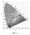
そのような色度図を図3に示す。当業者は、曲線310を上述の完全放射体軌跡として認識するであろう。図上のその他の特徴は、照明デバイスの特定の実施形態(1つ又は複数)を表わす。
Such a chromaticity diagram is shown in FIG. Those skilled in the art will recognize
具体的には、点P1及びP2はそれぞれ、第1の及び第2の発光素子で放射された光の色を表わす。これらの色は、P1とP2を結ぶ線分312が、かなりの部分にわたって、完全放射体軌跡310に密接に近似するように特に選択されている。図示されている実施形態において、3000K(2727℃)〜5000K(4727℃)の(完全放射体軌跡の)色温度範囲にわたって、CIE(x,y)平面上で、線分312が完全放射体軌跡310から離れている距離は0.005以下である。より広い、2500K(2227℃)〜5000K(4727℃)の色温度範囲にわたって、CIE(x,y)平面上で、線分312が完全放射体軌跡310から離れている距離は0.01以下である。
Specifically, points P1 and P2 represent the colors of light emitted by the first and second light emitting elements, respectively. These colors are specifically selected so that the
読者には、線分312が、第1の発光素子によって放射された光(P1で表わされる)と第2の発光素子によって放射された光(P2で表わされる)との線形組み合わせからなる出力を有する照明デバイスについて、全ての可能な光学出力群を表わしていることを、念頭に置かれたい。よって例えば、P1で表わされる光とP2で表わされる光が等量ずつからなっている光学出力の照明デバイスは、線分312を二分する点によって表わされる。点P1の光の割合が増大すると、デバイス出力点は線分312に沿って点P1に近づく。一方、点P2の光の割合が増大すると、デバイス出力点は線分312に沿って点P2に近づく。よって、第1の及び第2の発光素子によって放射された光の相対量を調節することによって、デバイス出力の色を変更又は調節することができる。
To the reader,
CIE色度図上のどの特定の色座標も、互いに実質的に異なり得る数多くの光学スペクトルを伴うことから、点P1、P2で表わされる色は、エレクトロルミネセンス光源と光変換素子の様々異なる組み合わせで達成することができる。そのような組み合わせは全て、本開示の範囲内である。しかしながら我々は、例えば、一方の点又はいずれかの点について正確に2つの別個のスペクトルピーク、あるいは、一方の点又はいずれかの点について正確に3つの別個のスペクトルピークなど、少数の別個のスペクトルピークの組み合わせを使用して、点P1、P2の一方又は両方を生成することが有利であることを見出した。 Since any particular color coordinate on the CIE chromaticity diagram is accompanied by a number of optical spectra that can be substantially different from each other, the colors represented by the points P1, P2 are different combinations of electroluminescent light sources and light conversion elements. Can be achieved. All such combinations are within the scope of this disclosure. However, we have a small number of separate spectra, for example, exactly two separate spectral peaks for one point or any point, or exactly three separate spectral peaks for one point or any point. It has been found advantageous to use a combination of peaks to generate one or both of points P1, P2.
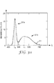
図示されている実施形態において、点P1で表わされる光は、2つの別個のスペクトルピークの組み合わせであり、その一方は点P1aで表わされ、もう一方は点P1bで表わされる。点P1aで表わされる光は典型的に、青色LEDで放射される光であり、そのピーク波長は約465nm、スペクトル幅(例えば、半値全幅(FWHM)値として測定される)が50nm未満、又は30nm未満、例えば25nmである。点P1bで表わされる光は、黄色燐光体(例えば、セリウムをドープしたイットリウムアルミニウムガーネット(YAG:Ce))が青色又はその他の短波長光で励起されたときにその燐光体から再発光された光を表わす。そのような再発光光は約550nmのピーク波長と、150nm、又は100nm未満のFWHMスペクトル幅を有し得る。図3aは、点P1、P1a、及びP1bの例証となるスペクトルS1を示す。具体的には、スペクトルS1は、第1のスペクトルピークS1aと、(部分的に重複した)第2のスペクトルピークS1bとの混合又は組み合わせである。第1のスペクトルピークS1aはピーク波長λpと、青色LEDによって放射された典型的な青色ポンプ光のスペクトル幅とを有し、この色は点P1aで表わされる。第2のスペクトルピークS1bはピーク波長λ1と、黄色燐光体からの典型的な再発光光のスペクトル幅とを有し、この色は点P1bで表わされる。好適な相対量又は比率での2つのスペクトルS1a、S1bの組み合わせは、結果として生じるスペクトルS1を生成し、この色は点P1で表わされる。図示されている実施形態において、この比率は、スペクトルピークS1bの積分強度が、スペクトルピークS1aの積分強度の約2.3倍になるように選択され、これにより生じる点P1の色は名目上白色である。スペクトルS1を有する光は、黄色の燐光体材料の層が上に適用された青色発光エレクトロルミネセンス光源を含む第1の発光素子によって生成され、ここにおいて燐光体層は好適な薄さを有するか、あるいは、青色ポンプ光の適切な一部を透過するよう設計されている。 In the illustrated embodiment, the light represented by point P1 is a combination of two distinct spectral peaks, one of which is represented by point P1a and the other is represented by point P1b. The light represented by point P1a is typically light emitted by a blue LED, whose peak wavelength is about 465 nm and whose spectral width (eg, measured as full width at half maximum (FWHM) value) is less than 50 nm, or 30 nm. Less than, for example, 25 nm. The light represented by point P1b is the light re-emitted from the phosphor when a yellow phosphor (eg, cerium-doped yttrium aluminum garnet (YAG: Ce)) is excited with blue or other short wavelength light. Represents. Such re-emitted light may have a peak wavelength of about 550 nm and a FWHM spectral width of less than 150 nm or 100 nm. FIG. 3a shows a spectrum S1 that is illustrative of points P1, P1a, and P1b. Specifically, the spectrum S1 is a mixture or combination of a first spectral peak S1a and a (partially overlapping) second spectral peak S1b. The first spectral peak S1a is the peak wavelength lambda p, and a spectral width of a typical blue pump light emitted by the blue LED, the color is represented by a point P1a. The second spectral peak S1b has a peak wavelength λ 1 and a spectral width of typical re-emitted light from a yellow phosphor, and this color is represented by the point P1b. The combination of the two spectra S1a, S1b in suitable relative amounts or ratios produces the resulting spectrum S1, whose color is represented by the point P1. In the illustrated embodiment, this ratio is selected so that the integrated intensity of the spectral peak S1b is approximately 2.3 times the integrated intensity of the spectral peak S1a, and the resulting color of the point P1 is nominally white. It is. The light having the spectrum S1 is generated by a first light-emitting element comprising a blue-emitting electroluminescent light source on which a layer of yellow phosphor material is applied, where the phosphor layer has a suitable thickness Alternatively, it is designed to transmit an appropriate part of the blue pump light.
同様に、図示されている実施形態において、点P2で表わされる光も、2つの別個のスペクトルピークの組み合わせであり、その一方は点P2aで表わされ、もう一方は点P2bで表わされる。点P2aで表わされる光は典型的に、図1及び2に関連して記述されるような再発光半導体構成体(RSC)の1つ以上のポテンシャル井戸によって、RSCが青色又はその他の短波長ポンプ光によって励起されたときに再発光された光である。この実施形態におけるそのようなポテンシャル井戸は、ピーク波長が約555nm、かつFWHMスペクトル幅が50nm未満、又は30nm未満、例えば、18nmである緑色光を再発光するよう設計される。点P2bで表わされる光はまた、短波長のポンプ光で照らされたときにRSCの1つ以上のポテンシャル井戸から再発光される光を表わすが、点P2bに関係するポテンシャル井戸は、点P2aに関係するポテンシャル井戸とは異なる。点P2bに関係するポテンシャル井戸は、ピーク波長が約620nm、かつFWHMスペクトル幅が50nm未満、又は30nm未満、例えば、18nmである赤色光を再発光するよう設計される。好適な相対量又は比率での2つのスペクトルS2a、S2bの組み合わせは、結果として生じるスペクトルS2を生成し、この色は点P2で表わされる。図示されている実施形態において、この比率は、スペクトルピークS2bの積分強度が、スペクトルピークS2aの積分強度の約2倍になるように選択され、これにより生じる点P2の色は実質的にアンバー色である。スペクトルS2を有する光は、好適に設計されたRSCが上に適用された青色又はその他の短波長ポンプ光発光エレクトロルミネセンス光源を含む第1の発光素子によって生成され、ここにおいてRSCは、ポンプ光を実質的にブロックするよう(スペクトルS2において、ポンプ波長λpで、顕著な強度がないことに注意)、かつ、スペクトルピークS2aを有する光とスペクトルピークS2bを有する光とを適正な比率で放射するよう設計されている。ポンプ光を実質的にブロックするためには、RSCには、波長λpでポンプ光源によって供給される短波長光この光はRSCのどの吸収層によっても吸収されないが、ポテンシャル井戸から生じる再発光光を大いに透過する)の実質的に全てを吸収するような光フィルタリング層が含まれ得、この層は時に「シアンブロッカー」と呼ばれる。この点に関しては、同時係属中の米国特許出願第61/175,636号「Re−Emitting Semiconductor Carrier Devices For Use With LEDs and Methods of Manufacture」(代理人整理番号第65435US002号)(2009年5月5日出願)が参照され、これは参照により本明細書に組み込まれる。完成品デバイスにおいて、そのような層は、RSCのポンプ光源に面する側とは反対側に含まれ得、すなわちこれにより、活性領域、特に活性領域のポテンシャル井戸が、ポンプ光源と光フィルタリング層(シアンブロッカー)との間に配置される。 Similarly, in the illustrated embodiment, the light represented by point P2 is also a combination of two distinct spectral peaks, one of which is represented by point P2a and the other is represented by point P2b. The light represented by point P2a is typically blue in RSC or other short wavelength pump due to one or more potential wells of a re-emitting semiconductor structure (RSC) as described in connection with FIGS. It is light re-emitted when excited by light. Such potential wells in this embodiment are designed to re-emit green light having a peak wavelength of about 555 nm and a FWHM spectral width of less than 50 nm, or less than 30 nm, eg, 18 nm. The light represented by point P2b also represents light that is re-emitted from one or more potential wells of the RSC when illuminated with short wavelength pump light, but the potential well associated with point P2b is at point P2a. Different from the related potential wells. The potential well associated with point P2b is designed to re-emit red light having a peak wavelength of about 620 nm and a FWHM spectral width of less than 50 nm, or less than 30 nm, eg, 18 nm. The combination of the two spectra S2a, S2b in a suitable relative amount or ratio produces the resulting spectrum S2, whose color is represented by the point P2. In the illustrated embodiment, this ratio is selected such that the integrated intensity of the spectral peak S2b is approximately twice the integrated intensity of the spectral peak S2a, and the resulting color at point P2 is substantially amber. It is. The light having spectrum S2 is generated by a first light-emitting element that includes a blue or other short wavelength pumped light emitting electroluminescent light source with a suitably designed RSC applied thereon, where RSC is the pump light In the spectrum S2 (note that there is no significant intensity at the pump wavelength λ p in the spectrum S2), and the light having the spectrum peak S2a and the light having the spectrum peak S2b are emitted at an appropriate ratio. Designed to do. In order to substantially block the pump light, the RSC includes a short wavelength light supplied by a pump light source at a wavelength λ p , which is not absorbed by any of the absorption layers of the RSC, but is a re-emitted light originating from a potential well An optical filtering layer that absorbs substantially all of this (which is highly transmissive) may sometimes be referred to as a “cyan blocker”. In this regard, co-pending U.S. Patent Application No. 61 / 175,636 “Re-Emitting Semiconductor Carriers For Use With LEDs and Methods of Manufacturing” (Attorney Docket No. 65435US2 Which is incorporated herein by reference. In the finished device, such a layer can be included on the opposite side of the RSC from the side facing the pump light source, i.e. the active region, in particular the potential well of the active region, is thus connected to the pump light source and the optical filtering layer ( (Cyan blocker).
図3aの前述の説明において、記号λ1は図1における意味とは多少異なる意味を有している、すなわち、この記号は図3aにおいては光変換素子からの再発光光に関連しているが、図1においてはエレクトロルミネセンスデバイスによって生成されたポンプ光に関連している。記号λ2は、図3bと1の両方において光変換素子からの再発光光に関連しており、これは、これら2つの図において同じ意味を有し得、あるいは多少異なる意味を有し得る。 In the above description of FIG. 3a, the symbol λ 1 has a slightly different meaning than that in FIG. 1, ie this symbol relates to the re-emitted light from the light conversion element in FIG. 3a. 1 relates to the pump light generated by the electroluminescent device. The symbol λ 2 is associated with the re-emitted light from the light conversion element in both FIGS. 3b and 1, which may have the same meaning or a slightly different meaning in these two figures.
図3bに示すスペクトルに類似の、2つのピーク波長を含むスペクトルを有する同時発光が可能なRSCを含んだ、代表的な半導体積層体を、下記の表2に示す。この積層体には、緑色スペクトルピークを生成する緑色発光(555nm)量子井戸1つと、赤色スペクトルピークを生成する赤色発光(620nm)量子井戸1つが含まれる。緑色及び赤色のピークの相対的強度は、主として、それぞれの量子井戸に関連する吸収材層の厚さによって制御される。緑色発光量子井戸に隣接した比較的薄い吸収材層を用いることによって、より多くのポンプ光がこれらの層を通過し、赤色発光量子井戸に隣接した吸収材層に吸収される。これにより、緑色光よりも赤色光が多い放射光をもたらすことができる。緑色光の赤色光に対する比率は、光取り出し特性の存在によってもある程度影響を受ける(例えば、そのような特性が、シアンブロッカーの外側表面にエッチング又は付着されている場合)。 A representative semiconductor stack comprising RSC capable of simultaneous emission with a spectrum containing two peak wavelengths similar to that shown in FIG. 3b is shown in Table 2 below. The stack includes one green emission (555 nm) quantum well that produces a green spectrum peak and one red emission (620 nm) quantum well that produces a red spectrum peak. The relative intensity of the green and red peaks is controlled primarily by the thickness of the absorber layer associated with each quantum well. By using a relatively thin absorber layer adjacent to the green light emitting quantum well, more pump light passes through these layers and is absorbed by the absorber layer adjacent to the red light emitting quantum well. This can provide radiated light that has more red light than green light. The ratio of green light to red light is also affected to some extent by the presence of light extraction characteristics (eg, if such characteristics are etched or adhered to the outer surface of the cyan blocker).
当業者には、様々な層について記載のバンドギャップエネルギーを達成するようにCdMgZnSe合金の組成を調整する方法が理解されるであろう。例えば、CdMgZnSe合金のバンドギャップエネルギーは主に、Mg成分によって制御される。量子井戸の放射波長(又はエネルギー)は、Cd/Zn比と、量子井戸の正確な厚さの両方によって制御される。 One skilled in the art will understand how to adjust the composition of the CdMgZnSe alloy to achieve the described band gap energy for the various layers. For example, the band gap energy of a CdMgZnSe alloy is mainly controlled by the Mg component. The emission wavelength (or energy) of the quantum well is controlled by both the Cd / Zn ratio and the exact thickness of the quantum well.
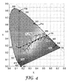
図3に類似の色度図を図4に示す。図4において、曲線310はここでも、上述のように完全放射体軌跡を表わす。ただし、図4には図3とは異なる特徴が含まれており、別の具体的な実施形態(1つ又は複数)の照明デバイスを表わしている。
A chromaticity diagram similar to FIG. 3 is shown in FIG. In FIG. 4,
具体的には、点P3及びP4はそれぞれ、第1の及び第2の発光素子で放射された光の色を表わす。(第1の及び第2の素子の一方又は両方は、図3に関連して説明される第1の及び第2の発光素子と異なっていてもよい。)これらの色は、P3とP4を結ぶ線分412が、かなりの部分にわたって、完全放射体軌跡310に密接に近似するように特に選択されている。図示されている実施形態において、3000K(2727℃)〜5000K(4727℃)の(完全放射体軌跡の)色温度範囲にわたって、CIE(x,y)平面上で、線分412が完全放射体軌跡310から離れている距離は0.005以下である。より広い、2500K(2227℃)〜5000K(4727℃)の色温度範囲にわたって、CIE(x,y)平面内で、線分312が完全放射体軌跡310から離れている距離は0.01以下である。一般に、上述の色温度範囲にわたって、CIE(x,y)平面上でこの線分が完全放射体軌跡から離れている距離は0.04以下、又は0。02以下であることが望ましい。
Specifically, points P3 and P4 represent the colors of light emitted by the first and second light emitting elements, respectively. (One or both of the first and second elements may be different from the first and second light emitting elements described in connection with FIG. 3). These colors are P3 and P4. The connecting
線分412は、第1の発光素子によって放射された光(P3で表わされる)と第2の発光素子によって放射された光(P4で表わされる)との線形組み合わせからなる出力を有する照明デバイスについて、全ての可能な光学出力群を表わしている。よって例えば、P3で表わされる光とP4で表わされる光が等量ずつからなっている光学出力の照明デバイスは、線分412を二分する点によって表わされる。点P3の光の割合が増大すると、デバイス出力点は線分412に沿って点P3に近づく。一方、点P4の光の割合が増大すると、デバイス出力点は線分412に沿って点P4に近づく。よって、第1の及び第2の発光素子によって放射された光の相対量を調節することによって、デバイス出力の色を変更又は調節することができる。
CIE色度図上のどの特定の色座標も、互いに実質的に異なり得る数多くの光学スペクトルを伴うことから、点P3、P4で表わされる色は、エレクトロルミネセンス光源と光変換素子の様々異なる組み合わせで達成することができる。そのような組み合わせは全て、本開示の範囲内である。しかしながら我々は、例えば、一方の点又はいずれかの点について正確に2つの別個のスペクトルピーク、あるいは、一方の点又はいずれかの点について正確に3つの別個のスペクトルピークなど、少数の別個のスペクトルピークの組み合わせを使用して、点P3、P4の一方又は両方を生成することが有利であることを見出した。 Since any particular color coordinate on the CIE chromaticity diagram is accompanied by a number of optical spectra that can be substantially different from each other, the colors represented by points P3 and P4 are different combinations of electroluminescent light sources and light conversion elements. Can be achieved. All such combinations are within the scope of this disclosure. However, we have a small number of separate spectra, for example, exactly two separate spectral peaks for one point or any point, or exactly three separate spectral peaks for one point or any point. It has been found advantageous to use a combination of peaks to generate one or both of points P3, P4.
図示されている実施形態において、点P3で表わされる光は、2つの別個のスペクトルピークの組み合わせであり、その一方は点P3aで表わされ、もう一方は点P3bで表わされる。点P3aで表わされる光は典型的に、青色LEDで放射される光であり、そのピーク波長は約465nm、FWHMスペクトル幅は50nm未満、又は30nm未満、例えば、18nmである。点P3bで表わされる光は、図1及び2に関連して記述されるようなRSCの1つ以上のポテンシャル井戸から、RSCが青色又はその他の短波長ポンプ光によって励起されたときに再発光された光を示すものである。この実施形態におけるそのようなポテンシャル井戸は、ピーク波長が約530nm、かつFWHMスペクトル幅が50nm未満、又は30nm未満、例えば、18nmである光を再発光するよう設計される。図4aは、点P3、P3a、及びP3bの例証となるスペクトルS3を示す。具体的には、スペクトルS3は、第1のスペクトルピークS3aと、第2のスペクトルピークS3bとの混合又は組み合わせである。第1のスペクトルピークS3aは、ピーク波長λpと、青色LEDによって放射された典型的な青色ポンプ光のスペクトル幅とを有し、この色は点P3aで表わされる。第2のスペクトルピークS3bは、ピーク波長λ4と、RSCの好適に設計された1つ以上のポテンシャル井戸により再発光された光を表わすスペクトル幅とを有し、この色は点P3bによって表わされる。好適な相対量又は比率での2つのスペクトルS3a、S3bの組み合わせは、結果として生じるスペクトルS3を生成し、この色は点P3で表わされる。図示されている実施形態において、この比率は、スペクトルピークS3bの積分強度が、スペクトルピークS3aの積分強度の約1.5倍になるように選択され、これにより生じる点P3の色は実質的にシアン色である。スペクトルS3を有する光は、好適に設計されたRSCが上に適用された青色発光エレクトロルミネセンス光源を含む第1の発光素子によって生成され、ここにおいてRSCは、青色ポンプ光の適切な量を透過するよう設計されている。そのようなRSCは典型的に、シアンブロッカー層を含まない。 In the illustrated embodiment, the light represented by point P3 is a combination of two distinct spectral peaks, one of which is represented by point P3a and the other is represented by point P3b. The light represented by point P3a is typically light emitted by a blue LED, which has a peak wavelength of about 465 nm and a FWHM spectral width of less than 50 nm, or less than 30 nm, for example, 18 nm. The light represented by point P3b is re-emitted from one or more potential wells of the RSC as described in connection with FIGS. 1 and 2 when the RSC is excited by blue or other short wavelength pump light. Light. Such potential wells in this embodiment are designed to re-emit light having a peak wavelength of about 530 nm and a FWHM spectral width of less than 50 nm, or less than 30 nm, eg, 18 nm. FIG. 4a shows a spectrum S3 that is illustrative of points P3, P3a, and P3b. Specifically, the spectrum S3 is a mixture or combination of the first spectrum peak S3a and the second spectrum peak S3b. The first spectral peak S3a has a peak wavelength lambda p, the spectral width of a typical blue pump light emitted by the blue LED, the color is represented by a point P3a. The second spectral peak S3b has a peak wavelength λ 4 and a spectral width representing light re-emitted by one or more well-designed potential wells of the RSC, this color being represented by the point P3b. . The combination of the two spectra S3a, S3b in a suitable relative amount or ratio produces the resulting spectrum S3, this color being represented by the point P3. In the illustrated embodiment, this ratio is selected such that the integrated intensity of the spectral peak S3b is approximately 1.5 times the integrated intensity of the spectral peak S3a, and the resulting color of the point P3 is substantially It is cyan. The light having spectrum S3 is generated by a first light emitting element that includes a blue emitting electroluminescent light source onto which a suitably designed RSC is applied, where the RSC transmits an appropriate amount of blue pump light. Designed to do. Such RSCs typically do not include a cyan blocker layer.
同様に、図示されている実施形態において、点P4で表わされる光も、2つの別個のスペクトルピークの組み合わせであり、その一方は点P4aで表わされ、もう一方は点P4bで表わされる。点P4aで表わされる光は典型的に、RSCの1つ以上のポテンシャル井戸によって、RSCが青色又はその他の短波長ポンプ光によって励起されたときに再発光された光である。この実施形態におけるそのようなポテンシャル井戸は、ピーク波長が約560nm、かつFWHMスペクトル幅が50nm未満、又は30nm未満、例えば18nmである黄緑色光を再発光するよう設計される。点P4bで表わされる光はまた、短波長のポンプ光で照らされたときにRSCの1つ以上のポテンシャル井戸から再発光される光を表わすが、点P4bに関係するポテンシャル井戸は、点P4aに関係するポテンシャル井戸とは異なる。点P4bに関係するポテンシャル井戸は、ピーク波長が約620nm、かつFWHMスペクトル幅が50nm未満、又は30nm未満、例えば、18nmである赤色光を再発光するよう設計される。好適な相対量又は比率での2つのスペクトルS4a、S4bの組み合わせは、結果として生じるスペクトルS4を生成し、この色は点P4で表わされる。図示されている実施形態において、この比率は、スペクトルピークS4bの積分強度が、スペクトルピークS4aの積分強度の約1.7倍になるように選択され、これにより生じる点P4の色は実質的にアンバー色である。スペクトルS4を有する光は、好適に設計されたRSCが上に適用された青色又はその他の短波長ポンプ光発光エレクトロルミネセンス光源を含む第1の発光素子によって生成され、ここにおいてRSCは、ポンプ光を実質的にブロックするよう(スペクトルS4において、ポンプ波長λpで、顕著な強度がないことに注意)、かつ、スペクトルピークS4aを有する光とスペクトルピークS4bを有する光とを適正な比率で放射するよう設計されている。ポンプ光を実質的にブロックするために、RSCは上述のように、例えば、シアンブロッカーなどの光フィルタリング層を含み得る。 Similarly, in the illustrated embodiment, the light represented by point P4 is also a combination of two distinct spectral peaks, one of which is represented by point P4a and the other is represented by point P4b. The light represented by point P4a is typically light that is re-emitted by one or more potential wells of the RSC when the RSC is excited by blue or other short wavelength pump light. Such potential wells in this embodiment are designed to re-emit yellow-green light with a peak wavelength of about 560 nm and a FWHM spectral width of less than 50 nm, or less than 30 nm, for example 18 nm. The light represented by point P4b also represents light that is re-emitted from one or more potential wells of the RSC when illuminated with short wavelength pump light, but the potential well associated with point P4b is at point P4a. Different from the related potential wells. The potential well associated with point P4b is designed to re-emit red light having a peak wavelength of about 620 nm and a FWHM spectral width of less than 50 nm, or less than 30 nm, eg, 18 nm. The combination of the two spectra S4a, S4b in a suitable relative amount or ratio produces the resulting spectrum S4, this color being represented by the point P4. In the illustrated embodiment, this ratio is selected such that the integrated intensity of the spectral peak S4b is approximately 1.7 times the integrated intensity of the spectral peak S4a, and the resulting color of the point P4 is substantially Amber color. The light having spectrum S4 is generated by a first light-emitting element that includes a blue or other short wavelength pumped light emitting electroluminescent light source with a suitably designed RSC applied thereon, where RSC is the pump light In the spectrum S4 (note that there is no significant intensity at the pump wavelength λ p in the spectrum S4), and the light having the spectrum peak S4a and the light having the spectrum peak S4b are emitted at an appropriate ratio. Designed to do. To substantially block the pump light, the RSC may include a light filtering layer, such as a cyan blocker, as described above.
まとめると、例えば、白色光を放射する発光素子を、アンバー光発光素子と組み合わせることによって、又は、シアン光発光素子を、アンバー光発光素子と組み合わせることによって、白色光の光学出力をもたらすことができる光源デバイスがこれまでで記述された。更に、白色光出力の特定の色又は色温度は、異なる発光素子によって設けられる光の相対的混合比を調節することによって調節することができ、この調節された白色光は、CIE色度図上の表示で、幅広い色温度にわたって完全放射体軌跡上に沿うか又は非常に近くに示される色を有し得る。 In summary, for example, by combining a light emitting element that emits white light with an amber light emitting element, or by combining a cyan light emitting element with an amber light emitting element, an optical output of white light can be provided. A light source device has been described so far. In addition, the specific color or color temperature of the white light output can be adjusted by adjusting the relative mixing ratio of the light provided by the different light emitting elements, and this adjusted white light is shown on the CIE chromaticity diagram. May have colors shown along or very close to the full radiator trajectory over a wide range of color temperatures.
更に、我々は、図3、3a、3b、及び4、4a、4bに関連して記述されたタイプの実施形態が、非常に良好な「演色」性を有利に呈することも見出した。「演色評価数」(CRI)は、目による直接観測によって知覚されるデバイス光学出力の見かけ又は色だけでなく、例えばそのデバイス光学出力を用いた反射光内で見られる対象物又は物品の見かけにも関心がある照明デバイス設計者にとって、重要であり得るパラメーターである。対象物又は物品の反射率スペクトルに応じて、その見かけは、第1の名目上白色光源で照らされたときと、第2の名目上白色光源で照らされたときとでは、たとえその第1と第2の白色光源がCIE色度図上で同一の色座標を有していたとしても、非常に異なることがある。これは、CIE色度図上での特定の色座標が、互いに実質的に異なり得る数多くの光学的スペクトルに関連付けられ得るという事実からの帰結である。演色性の影響を示す一般的な実例は、着色した対象物が太陽光で照らされたとき、例えば、オフィスの蛍光灯で照らされたときと比べて、又はガス放電灯で照らされたときと比べて、これらの照明光源がどれも直接見たときには名目上白色に見え得るにもかかわらず、非常に違って見えるということである。 Furthermore, we have also found that embodiments of the type described in connection with FIGS. 3, 3a, 3b and 4, 4a, 4b advantageously exhibit very good “color rendering” properties. “Color rendering index” (CRI) is not only the appearance or color of the device optical output perceived by direct observation by the eye, but also the appearance of the object or article seen in the reflected light using that device optical output, for example. Is also a parameter that can be important for lighting device designers who are also interested. Depending on the reflectance spectrum of the object or article, its appearance may be the first and second when illuminated with a first nominally white light source, and when illuminated with a second nominally white light source. Even if the second white light source has the same color coordinates on the CIE chromaticity diagram, it can be very different. This is a consequence of the fact that a particular color coordinate on the CIE chromaticity diagram can be associated with a number of optical spectra that can be substantially different from each other. A common example of the effect of color rendering is when a colored object is illuminated with sunlight, for example compared to when illuminated with an office fluorescent light or when illuminated with a gas discharge lamp. In comparison, all of these illumination sources look very different when viewed directly, even though they may appear nominally white.
所与の光源の演色評価数は、CIE出版物13.3−1995「Method of Measuring and Specifying Colour Rendering Properties of Light Sources」に記述されている方法を用いて測定することができる。演色評価数は一般に、下が0、上が100までの範囲の値であり、値が大きいほど一般に望ましい。更に、CIE 13.3−1995出版物に基づき、所与の光源を表わす所与のスペクトルの演色評価数を計算できる数値的技法及びソフトウェアが、CIEから入手できる。 The color rendering index for a given light source can be measured using the method described in CIE Publication 13.3-1995 “Method of Measuring and Specifying Color Rendering Properties of Light Sources”. In general, the color rendering index is a value in the range of 0 to 100 and 100 to the top, and a larger value is generally desirable. In addition, numerical techniques and software are available from the CIE that can calculate a color rendering index for a given spectrum representing a given light source based on the CIE 13.3-1995 publication.
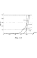
そのようなソフトウェアを使用して、図3a及び3bに示されているスペクトルS1及びS2の線形組み合わせからなるデバイス光学出力の演色評価数を算出した場合、その結果は、色温度範囲2500K(2227℃)〜5000K(4727℃)(スペクトルS1及びS2の様々な比率に対応)にわたって、演色評価数が少なくとも80である。図3a/3bの実施形態に関するこの演色評価数を、図5の曲線510に示し、この図では、算出された演色評価数(CRI)が、デバイス出力全体の色温度に対してプロットされている。同様に、同じソフトウェアを使用して、図4a及び4bに示されているスペクトルS3及びS4の線形組み合わせからなるデバイス光学出力の演色評価数を算出した場合、その結果は、ここでも、色温度範囲2500K(2227℃)〜5000K(4727℃)(スペクトルS3及びS4の様々な比率に対応)にわたって、演色評価数が少なくとも80である。この図4a/4bの実施形態に関するこの演色評価数を、図5の曲線512に示す。図5には、もう1つの曲線514も描かれている。この曲線514は、図3/3a/3bの実施形態に類似であるが、ただし第2の発光素子(例えば、青色LEDポンプRSCで、その光出力は図3の点P2と、図3bのスペクトルS2によって特性付けられる)を、アンバー発光LEDを有するがRSC又はその他の光変換素子は有さないような発光素子に置き換えた実施形態について算出したCRIであり、このアンバー発光LEDは、ピーク波長592nmの単一スペクトルピークの光を放射し、これにより、CIE色度図上の色はここでも実質的に、図3の点P2に対応する。曲線514を曲線510と比較すると、CIE色度図上のプロットでは実質的に同じ色特性を有する2つのデバイスが、非常に異なる演色性を有し得るということがわかるであろう。
If such software was used to calculate the color rendering index of the device optical output consisting of the linear combination of spectra S1 and S2 shown in FIGS. 3a and 3b, the result is the color temperature range 2500K (2227 ° C. ) To 5000K (4727 ° C.) (corresponding to various ratios of spectra S1 and S2), the color rendering index is at least 80. This color rendering index for the embodiment of FIGS. 3a / 3b is shown in
代表的な実施形態において、開示されるデバイスの演色評価数は、例えば、2500K(2227℃)〜5000K(4727℃)の色温度範囲、又は3000K(2727℃)〜5000K(4727℃)の色温度範囲にわたって、少なくとも60、又は少なくとも70、又は少なくとも80である。高い演色評価数を達成するためには、デバイス光学出力を形成する構成成分スペクトル(S1,S2)それぞれが、少なくとも2つの個別のスペクトルピークで特性付けられ(例えば、図3aのピークS1a、S1b、又は図3bのピークS2a、S2b)、これらのピークは、例えば、互いに少なくとも10nm離れている可能性がある。更に、デバイス光学出力を形成する構成成分スペクトルそれぞれが、例えば、正確に2つの別個のスペクトルピークによって、又は正確に3つの別個のスペクトルピークによって特徴付けられる。 In an exemplary embodiment, the color rendering index of the disclosed device is, for example, a color temperature range of 2500K (2227 ° C) to 5000K (4727 ° C), or a color temperature of 3000K (2727 ° C) to 5000K (4727 ° C). Over the range is at least 60, or at least 70, or at least 80. In order to achieve a high color rendering index, each of the component spectra (S1, S2) forming the device optical output is characterized by at least two separate spectral peaks (eg, peaks S1a, S1b, Or the peaks S2a, S2b) of FIG. 3b, these peaks may be at least 10 nm apart from each other, for example. Furthermore, each component spectrum that forms the device optical output is characterized, for example, by exactly two distinct spectral peaks or by exactly three distinct spectral peaks.
代表的なデバイスの望ましい色関連特性を記述したところで、次に、このデバイスの様々な構成要素を物理的にどのように配置できるかを非制限的な意味で解説する幾つかの図を見ていく。 Having described the desired color-related characteristics of a typical device, let's now look at some diagrams that illustrate in a non-limiting sense how the various components of this device can be physically located. Go.
図6は、代表的な照明デバイス610の概略断面図である。このデバイスには、第1の発光素子612と、第2の発光素子614とが含まれ、両方とも金属ヘッダー616上に取り付けられている。ヘッダー616は、ヘッダーに一体化している第1導電性ポスト618と、第2及び第3導電性ポスト620、622とを有し、これらは互いに電気的に絶縁され、また素子612、614が取り付けられているヘッダーのディスク形状主部分からも絶縁されている。ポスト620は、ワイヤ624及びワイヤ接着を介して、第1の発光素子612の第1の電気接触に電気的に結合しており、同様にポスト622は、ワイヤ626及びワイヤ接着を介して、第2の発光素子614の第1の電気接触に電気的に結合している。第1の及び第2の発光素子は更にそれぞれ、第2の電気接触を有し、これらは両方とも、ヘッダー616のディスク形状主部分とオーム接触し、すなわち、ポスト618ともオーム接触している。
FIG. 6 is a schematic cross-sectional view of a
第1の発光素子612には、第1のポンプ光を放射する第1のエレクトロルミネセンス光源612aと、第1のポンプ光の少なくとも一部分を第1の再発光光構成成分へと変換する第1の光変換素子612bとが含まれる。光源612aは、LED、レーザーダイオード、又は同様のソリッドステートエレクトロルミネセンス光源で、好適な強度とスペクトルのポンプ光を放射するよう適合されたものであり得る。上述の第1の発光素子612の第1の及び第2の電気接触は、光源612a上に提供され、これにより、ポスト618、620に対して印加される第1の電気信号に応答してポンプ光を放射することができる。光変換素子612bは、例えば、1つ以上のRSC、及び/又は1つ以上の燐光体であってもよく、又はこれらを含んでもよい。光源612aと素子612bが協働することにより、素子612が第1のスペクトル分布を有する光612cを放射する。光612cは、典型的に少なくとも、素子612bからの第1の再発光光構成要素を含み、更に上述のように、光612cの望ましいスペクトル特性に応じて、光源612aによって放射された第1のポンプ光の一部も含み得る。
The first
第2の発光素子614には、第2のポンプ光を放射する第2のエレクトロルミネセンス光源614aと、その第2のポンプ光の少なくとも一部を第2の再発光光構成成分へと変換する第2の光変換素子614bとが含まれる。光源614aは、LED、レーザーダイオード、又は同様のソリッドステートエレクトロルミネセンス光源で、好適な強度とスペクトルのポンプ光を放射するよう適合されたものであり得る。上述の第2の発光素子614の第1の及び第2の電気接触は、光源614a上に提供され、これにより、ポスト618、622に対して印加される第2の電気信号に応答してポンプ光を放射することができる。光変換素子614bは、例えば、1つ以上のRSC、及び/又は1つ以上の燐光体であってよく、又はこれらを含んでもよい。好ましくは、光変換素子612bと光変換素子614bのうち少なくとも1つが、少なくとも1つのポテンシャル井戸を含む。光源614aと素子614bが協働することにより、素子614が第2のスペクトル分布を有する光614cを放射する。光614cは典型的に少なくとも、素子614bからの第2の再発光光構成要素を含み、更に上記で詳述されているように、光614cの望ましいスペクトル特性に応じて、光源614aによって放射されたポンプ光の一部も含み得る。
The second light-emitting
自由空間伝搬によって、又は光学ディフューザー、レンズ、ミラー、及び同様物などのメカニズムによって、及び所望により他の光構成要素と共に、光612cと光614cとを合わせることによって、矢印628で概略的に図示されるデバイス610のデバイス光学出力を生成する。よってデバイス光学出力628は、いくらかの量の光612cといくらかの量の光614cとを含む。出力628中に存在する光612c、614cの相対量は、デバイス出力628の知覚色(例えば、色温度)を制御する。これらの相対量、よってすなわち、デバイス出力色は、異なる発光素子612、614の独立した又は別個の電気的制御によって制御することができる。よって、第1の発光素子612は、第1の電気信号(例えば、所与の大きさの電流)をポスト618、620にわたって印加することによってエネルギーを与えることができる。第2の発光素子614は、第1の電気信号とは独立及び/又は個別の第2の電気信号をポスト618、622に印加することによってエネルギーを与えることができる。第1の及び第2の電気信号の大きさは、第1の及び第2の発光素子612、614によって放射される光の量、並びに出力628の色温度を制御するのに使用される。
Illustrated schematically by
図7は、デバイス610に類似の代表的な照明デバイス710の概略断面図である。同様の参照番号は同様の要素を指し示し、これらの更なる説明は不要である。デバイス710には、第1の発光素子712と、第2の発光素子714とが含まれ、両方とも金属ヘッダー616上に取り付けられている。ポスト620は、第1の発光素子712の第1の電気接触に電気的に結合しており、ポスト622は、第2の発光素子714の第1の電気接触に電気的に結合している。第1の及び第2の発光素子は更にそれぞれ、第2の電気接触を有し、これらは両方とも、ヘッダー616のディスク形状主部分とオーム接触し、すなわち、ポスト618ともオーム接触している。
FIG. 7 is a schematic cross-sectional view of an
第1の及び第2の発光素子712、714は上述の素子612、614に類似であり、第1の素子712は、第1のポンプ光を放射する第1のエレクトロルミネセンス光源712aと、その第1のポンプ光の少なくとも一部を第1の再発光光構成成分に変換する第1の光変換素子712bとを含み、第2の素子714は、第2のポンプ光を放射する第2のエレクトロルミネセンス光源714aと、その第2のポンプ光の少なくとも一部を第2の再発光光構成成分に変換する第2の光変換素子714bとを含む。エレクトロルミネセンス光源712a、714aは、光源612a、614aが別個の半導体(例えば、LED)チップによって提供され、一方光源712a、714aは、同じ半導体(例えば、LED)チップ上の別個のpn接合によって提供されている限りにおいて、光源612a、614aとは異なる。しかしながら両方の場合において、第1の及び第2のエレクトロルミネセンス光源(612a及び614a、又は712a及び714a)は、別個の電気信号によって、独立に及び/又は別個に制御可能である。また、両方の場合において、第1の及び第2のエレクトロルミネセンス光源は、同じスペクトルを有するポンプ光を放射することがあり、又は異なるスペクトルのポンプ光を放射することがある。
The first and second
上述の第1の発光素子712の第1の及び第2の電気接触は、光源712a上に設けられ、これにより、ポスト618、620に対して印加される第1の電気信号に応答して第1のポンプ光を放射することができる。光変換素子712bは、例えば1つ以上のRSC、及び/又は1つ以上の燐光体であってもよく、又はこれらを含んでもよい。光源712aと素子712bが協働することにより、素子712が第1のスペクトル分布を有する光712cを放射する。第2の発光素子714の第1の及び第2の電気接触は、光源714a上に設けられ、これにより、ポスト618、622に対して印加される第2の電気信号に応答して第2のポンプ光を放射することができる。光変換素子714bは、例えば、1つ以上のRSC、及び/又は1つ以上の燐光体であってよく、又はこれらを含んでもよいが、しかしながら好ましくは、光変換素子712bと光変換素子714bのうち少なくとも1つが、少なくとも1つのポテンシャル井戸を含む。光源714aと素子714bが協働することにより、素子714が第2のスペクトル分布を有する光714cを放射する。光714cは典型的に少なくとも、素子714bからの第2の再発光光構成要素を含み、更に上述のように、光714cの望ましいスペクトル特性に応じて、光源714aによって放射されたポンプ光の一部も含み得る。
The first and second electrical contacts of the first
図6のデバイスとは異なり、図7では、一体型光変換層が、エレクトロルミネセンス光源712a及びエレクトロルミネセンス光源714aの両方を覆うように提供され、その一体型光変換層の一部が第1の光変換素子712bを形成し、その一体型光変換層の別の一部が第2の光変換素子714bの一部を形成している。図7に見られるように、第2の光変換素子714bは更に、第1の光変換素子712b内にはないもう1つの光変換素子を含んでいる。
Unlike the device of FIG. 6, in FIG. 7, an integrated light conversion layer is provided to cover both the electroluminescent
自由空間伝搬によって、又は光学ディフューザー、レンズ、ミラー、及び同様物などのメカニズムによって、及び所望により他の光構成要素と共に、光712cと光714cとを合わせることによって、矢印728で図示されるデバイス710のデバイス光学出力を生成する。出力728中に存在する光712c、714cの相対量は、デバイス出力728の色温度又はその他の知覚色を制御する。これらの相対量、すなわちデバイス出力色は、異なる発光素子712、714の独立した又は別個の電気的制御によって制御することができる。よって、第1の発光素子712は、第1の電気信号をポスト618、620に印加することによってエネルギーを与えることができ、第2の発光素子714は、第1の電気信号とは独立及び/又は個別の第2の電気信号をポスト618、622に印加することによってエネルギーを与えることができる。第1の及び第2の電気信号の大きさは、第1の及び第2の発光素子712、714によって放射される光の量、並びに出力728の色温度を制御するのに使用される。
図8は、別の照明デバイス810の概略平面図であり、デバイス610(図6)又は710(図7)のいずれかに実質的に適用できる設計である。デバイス810には、第1の発光素子812と第2の発光素子814とが含まれる。細い線幅を有する全体に正方形の電気接触812aは、第1の素子812の第1のエレクトロルミネセンス光源上に設けられる。この素子812はまた、正方形の接触812aに囲まれている素子812の中央領域に少なくとも配置されている第1の光変換素子812bを含む。素子812の周辺領域812cは更に、第1の光変換素子812bで覆われていてもよく、又は、光変換素子を含まずに、むしろ単に第1のエレクトロルミネセンス光源の露出部分であってもよい。
FIG. 8 is a schematic plan view of another
細い線幅を有するもう1つの全体に正方形の電気接触814も、第2の素子814の第2のエレクトロルミネセンス光源814上に設けられる。この素子814はまた、正方形の接触814aに囲まれている素子814の中央領域に少なくとも配置されている第2の光変換素子814bを含む。素子812の周辺領域814cは更に、第2の光変換素子812bで覆われていてもよく、又は、光変換素子を含まずに、むしろ単に第2のエレクトロルミネセンス光源の露出部分であってもよい。
Another generally square
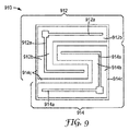
図9は、別の照明デバイス910の概略平面図であり、例えば、デバイス710(図7)に実質的に適用できる設計である。デバイス910は、第1の全体にU字形の発光素子912と、第2の全体にU字形の発光素子914とを含み、これら2つの素子が相互に噛み合うパターンを形成し、これにより全体に正方形の全外形又は境界線がもたらされる。細い線幅を有する全体にU字形の電気接触912aは、第1の素子912の第1のエレクトロルミネセンス光源上に設けられる。素子912は更に、接触912aに近接した領域において第1のエレクトロルミネセンス光源上に配置された第1の光変換素子912bを含む。
FIG. 9 is a schematic plan view of another
細い線幅を有するもう1つの全体にU字形の電気接触914aも、第2の素子914の第2のエレクトロルミネセンス光源上に設けられる。素子914は更に、接触914aに近接した領域において第2のエレクトロルミネセンス光源上に配置された第2の光変換素子914bを含む。
Another generally U-shaped
デバイス910の残り領域914cは、第1の光変換素子912b及び/又は第2の光変換素子914bで覆われていてもよく、あるいは、光変換素子を含まずに、むしろ単に第1の及び/又は第2のエレクトロルミネセンス光源の露出部分であってもよい。デバイス910の指趾間状デザインにより、エレクトロルミネセンス素子912及び914からの光の混合が促進され得る。
The remaining area 914c of the
図6及び7の実施形態は、照明デバイスの2つの発光素子が3つの電気端子又は接触を使用していかにして独立に制御することができるかを示しており、ここにおいて1つの端子(ポスト618)は両方の素子に共通であり、他の端子(ポスト620、622)のそれぞれは、素子の一方のみに専用のものである。独立制御は、1組の端子(ポスト618、620)に対して第1の電気信号を適用し、別の1組の端子(ポスト618、622)に対して第2の電気信号(第1の電気信号とは独立)を適用することにより達成できる。もちろん、4端子デバイスも想到され、ここにおいて両方の素子に共通する端子はなく、所与の組の端子が、発光素子の所与の一方に専用のものとなる。
The embodiment of FIGS. 6 and 7 shows how the two light emitting elements of the lighting device can be controlled independently using three electrical terminals or contacts, where one terminal (post 618) is common to both elements, and each of the other terminals (
図10において、我々は、入力端子2つだけを有する回路1010を開示し、これは、開示される照明デバイスの2つの発光素子を異なる量で駆動するのに使用することができ、これにより、2つの入力端子に供給される電気入力の大きさの関数として、カラー制御又は調節を達成することができる。この回路において、端子1012及び1014は入力端子である。外部変数又は調節可能な供給源1016は、図示のように、入力端子の間に連結される。供給源1016は、電圧源又は電流であり得、これが照明デバイスに、可変電圧Vs及び可変電流Iを供給する。照明デバイスは、第1のエレクトロルミネセンス光源と、その第1のエレクトロルミネセンス光源から供給されたポンプ光の少なくとも一部を第1の再発光光構成成分へと変換する第1の光変換素子とを有する第1の発光素子を含む。この照明デバイスは更に、第2のエレクトロルミネセンス光源と、その第2のエレクトロルミネセンス光源によって供給されたポンプ光の少なくとも一部を第2の再発光光構成成分へと変換する第2の光変換素子とを有する、第2の発光素子を含む。
In FIG. 10, we disclose a
回路1010において、第1のエレクトロルミネセンス光源は、例えば、LEDであってもよく、又はLEDを含んでもよく、ダイオードD1として表わされ、第2のエレクトロルミネセンス光源は、別のLEDであってよく、又は別のLEDを含んでもよく、ダイオードD2として表わされる。このダイオードは図示のように別の回路要素(すなわちトランジスタQ1及びQ2、並びにベース抵抗Rb)に接続され、回路1010を完結している。ダイオードD1、ダイオードD2、及びベース抵抗Rbを通過する電流はそれぞれ、I1、I2、及びI3とラベル付けされる。これらの電流を加算して、ソース電流Iとなる、すなわち、I1+I2+I3=Iである。接続されたトランジスタQ1及びベース抵抗Rbにより、電流I1がダイオードD1中を流れ、主にRbとトランジスタQ1の電流利得によって決定される値に実質的に制限されることに注意されたい。一方、トランジスタQ2は、ダイオードとして機能するように接続され、これによりダイオードD2は、ダイオードD1を含む回路の分岐が飽和するまでの間、ほとんど通電状態にはならない。
In
入力端子1012、1014に対して印加される電気信号へのこのような応答の違いが、ダイオードD1及びD2によって放射される光の相対量の違いを引き起こし、これにより、照明デバイスの第1の及び第2の発光素子によって放射される光の相対量の違いが生じ、これにより、印加される電気信号の大きさの関数として、照明デバイス光学出力によって設けられる色又は色温度の違いが生じる。例えば、第1の発光素子(ダイオードD1を一部に含む)は暖かい白色光を放射し、第2の発光素子(ダイオードD2を一部に含む)は冷たい白色光を放射する場合、回路1010の効果は、低印加電流で実質的に暖かい白色光の組み合わせ出力(すなわち、照明デバイスの光学出力)を提供するが、この出力は、印加電流が増加するに従い、徐々に冷たく明るい白色に移行する。そのような性能は、なじみ深い白熱光源の減光動作に似ているため、望ましいことがある。回路1010はよって、色変化の減光回路として動作し得る。
Such a difference in response to electrical signals applied to the
完全性のために、図11a及び11bは、回路1010のモデル化動作を示している。ここでRbの値は500オームと仮定された。両方の図において、y軸は、所与の回路素子(1つ又は複数)を通って流れる電流をミリアンペアで表わす。図11aにおいて、x軸は、外部電源によって供給される電圧Vsを表わす。曲線1110はダイオードD1を通って流れる電流I1を表わし、曲線1112はダイオードD2を通って流れる電流I2を表わし、曲線1114はこれらの電流の合計I1+I2を表わす。図11bにおいて、x軸は、両方のダイオードを通って流れる合計電流、すなわちI1+I2を表わす。曲線1116はダイオードD1を通って流れる電流I1を表わし、曲線1118はダイオードD2を通って流れる電流I2を表わす。
For completeness, FIGS. 11 a and 11 b illustrate the modeling operation of
回路1010の1つ以上の構成要素(例えば、トランジスタ及び/又はベース抵抗)は、シリコン基材内、又は他の、「金属接着」GaN LEDに使用される半導体基材内に作製することができる。あるいは、そのような回路構成要素は物理的に別個に作製し、発光を担う半導体デバイスから離しておくことができる。 One or more components of the circuit 1010 (eg, transistors and / or base resistors) can be fabricated in a silicon substrate or other semiconductor substrate used for “metal bonded” GaN LEDs. . Alternatively, such circuit components can be made physically separate and away from the semiconductor device responsible for light emission.
特記しない限り、本明細書及び「特許請求の範囲」で使用されている量、性質の測定などを表現する全ての数は、用語「約」により改変されていると理解されるべきである。したがって、反することが示されない限り、本明細書及び添付の「特許請求の範囲」に記載の数値的パラメーターは、本発明の教示を利用して当業者により得ることが求められる所望の性質に応じて変化する近似値である。均等論を「特許請求の範囲」の範疇に適用することを制限しようとする試みとしてではなく、各数値パラメーターは少なくとも、記録された有効数字の桁数を考慮して、又通常の四捨五入を適用することによって解釈されるべきである。本発明の広範な範囲を示す数値範囲及びパラメーターは近似であるにもかかわらず、いかなる数値も本明細書で述べられる具体的な例で示される程度に、これらは妥当に可能な限り精確に報告される。しかしながら、いかなる数値も試験及び測定の限界に関連する誤差を含み得る。 Unless otherwise stated, all numbers expressing quantities, property measurements, etc. used in the specification and in the claims are to be understood as being modified by the term “about”. Accordingly, unless indicated to the contrary, the numerical parameters set forth herein and in the appended claims are dependent on the desired properties sought to be obtained by one of ordinary skill in the art using the teachings of the present invention. It is an approximate value that changes. Rather than trying to limit the application of the doctrine to the scope of the claims, each numeric parameter takes at least the number of significant digits recorded and applies normal rounding Should be interpreted. Although numerical ranges and parameters representing the broad scope of the present invention are approximate, any numerical values are reported as accurately as reasonably possible to the extent shown in the specific examples described herein. Is done. However, any numerical value may include errors associated with test and measurement limits.
本発明の様々な修正及び変更は、本発明の範囲及び趣旨から逸脱せずに当該技術分野の当業者に明らかとであり、本発明は、ここに記載された例示的な実施形態に限定されないことが理解されるべきである。例えば、1つの開示実施形態の特徴は、別に記載のない限り、他の開示実施形態全てにも適用され得ることを、読者は推定すべきである。また、本明細書において参照された全ての米国特許、公開特許出願、並びに他の特許及び非特許文書は、それらが上述の開示に矛盾しない範囲において、参照によって全てが組み込まれることが理解されるべきである。 Various modifications and alterations of this invention will become apparent to those skilled in the art without departing from the scope and spirit of this invention, and this invention is not limited to the exemplary embodiments described herein. It should be understood. For example, the reader should assume that the features of one disclosed embodiment may apply to all other disclosed embodiments unless otherwise stated. It is also understood that all US patents, published patent applications, and other patents and non-patent documents referred to herein are incorporated by reference to the extent they do not conflict with the above disclosure. Should.
Claims (23)
第1のポンプ光を放射する第1のエレクトロルミネセンス光源と、
前記第1のポンプ光の少なくとも一部を第1の再発光光構成成分に変換する第1の光変換素子と、を含んだ、第1のスペクトル分布を有する光を放射するよう構成された第1の発光素子と、
第2のポンプ光を放射する第2のエレクトロルミネセンス光源と、
前記第2のポンプ光の少なくとも一部を第2の再発光光構成成分に変換する第2の光変換素子と、を含んだ、第2のスペクトル分布を有する光を放射するよう構成された第2の発光素子と、を含み、
前記第1の及び前記第2の光変換素子のうち少なくとも1つが、第1のポテンシャル井戸を含む第1の半導体積層体を含み、
前記第1の及び前記第2の発光素子が、前記第1の及び前記第2の発光素子によって放射される光が組み合わせられてデバイス出力を供給するように配置され、
前記第1の及び前記第2のスペクトル分布は、標準CIE(x,y)色座標図上の線分上のそれぞれ第1の及び第2の終点によって表わすことができ、前記線分は、前記第1の発光素子によって放射された光と、前記第2の発光素子によって放射された光との、様々な相対量について、可能なデバイス出力の範囲を表わし、前記線分の少なくとも一部分が更に、少なくとも色温度範囲3000K(2727℃)〜5000K(4727℃)にわたって完全放射体軌跡に近似している、ソリッドステート照明デバイス。 A solid state lighting device,
A first electroluminescent light source that emits first pump light;
A first light converting element that converts at least a part of the first pump light into a first re-emitting light component, and configured to emit light having a first spectral distribution. 1 light emitting element;
A second electroluminescent light source that emits second pump light;
A second light converting element that converts at least a portion of the second pump light into a second re-emitting light component, and configured to emit light having a second spectral distribution. 2 light emitting elements,
At least one of the first and second light conversion elements includes a first semiconductor stack including a first potential well;
The first and second light emitting elements are arranged such that light emitted by the first and second light emitting elements is combined to provide a device output;
The first and second spectral distributions can be represented by first and second endpoints on a line segment on a standard CIE (x, y) color coordinate diagram, respectively, Representing a range of possible device outputs for various relative amounts of light emitted by the first light emitting element and light emitted by the second light emitting element, wherein at least a portion of the line segment further comprises: A solid-state lighting device that approximates a full radiator trajectory over at least a color temperature range of 3000K (2727 ° C) to 5000K (4727 ° C).
Applications Claiming Priority (3)
| Application Number | Priority Date | Filing Date | Title |
|---|---|---|---|
| US22166009P | 2009-06-30 | 2009-06-30 | |
| US61/221,660 | 2009-06-30 | ||
| PCT/US2010/040017 WO2011002686A1 (en) | 2009-06-30 | 2010-06-25 | White light electroluminescent devices with adjustable color temperature |
Related Child Applications (1)
| Application Number | Title | Priority Date | Filing Date |
|---|---|---|---|
| JP2015023239A Division JP6140742B2 (en) | 2009-06-30 | 2015-02-09 | White light electroluminescent device with adjustable color temperature |
Publications (2)
| Publication Number | Publication Date |
|---|---|
| JP2012532453A true JP2012532453A (en) | 2012-12-13 |
| JP2012532453A5 JP2012532453A5 (en) | 2013-08-08 |
Family
ID=42646301
Family Applications (2)
| Application Number | Title | Priority Date | Filing Date |
|---|---|---|---|
| JP2012517777A Pending JP2012532453A (en) | 2009-06-30 | 2010-06-25 | White light electroluminescent device with adjustable color temperature |
| JP2015023239A Expired - Fee Related JP6140742B2 (en) | 2009-06-30 | 2015-02-09 | White light electroluminescent device with adjustable color temperature |
Family Applications After (1)
| Application Number | Title | Priority Date | Filing Date |
|---|---|---|---|
| JP2015023239A Expired - Fee Related JP6140742B2 (en) | 2009-06-30 | 2015-02-09 | White light electroluminescent device with adjustable color temperature |
Country Status (7)
| Country | Link |
|---|---|
| US (1) | US8629611B2 (en) |
| EP (1) | EP2449856A1 (en) |
| JP (2) | JP2012532453A (en) |
| KR (1) | KR20120092549A (en) |
| CN (1) | CN102474932B (en) |
| TW (1) | TW201130107A (en) |
| WO (1) | WO2011002686A1 (en) |
Cited By (3)
| Publication number | Priority date | Publication date | Assignee | Title |
|---|---|---|---|---|
| JPWO2014119313A1 (en) * | 2013-01-31 | 2017-01-26 | 株式会社東芝 | Light emitting device and LED bulb |
| JP2017045928A (en) * | 2015-08-28 | 2017-03-02 | 日亜化学工業株式会社 | Light-emitting device |
| JP2022523868A (en) * | 2019-03-28 | 2022-04-26 | ルミレッズ リミテッド ライアビリティ カンパニー | Color Adjustable Light Emitting Diode (LED) Systems, LED Lighting Systems and Methods |
Families Citing this family (19)
| Publication number | Priority date | Publication date | Assignee | Title |
|---|---|---|---|---|
| WO2010129412A1 (en) | 2009-05-05 | 2010-11-11 | 3M Innovative Properties Company | Re-emitting semiconductor construction with enhanced extraction efficiency |
| US8994071B2 (en) | 2009-05-05 | 2015-03-31 | 3M Innovative Properties Company | Semiconductor devices grown on indium-containing substrates utilizing indium depletion mechanisms |
| EP2427924A1 (en) | 2009-05-05 | 2012-03-14 | 3M Innovative Properties Company | Re-emitting semiconductor carrier devices for use with leds and methods of manufacture |
| WO2011008474A1 (en) | 2009-06-30 | 2011-01-20 | 3M Innovative Properties Company | Electroluminescent devices with color adjustment based on current crowding |
| CN102473817A (en) | 2009-06-30 | 2012-05-23 | 3M创新有限公司 | Cadmium-free re-emitting semiconductor construction |
| US9159885B2 (en) | 2010-12-29 | 2015-10-13 | 3M Innovative Properties Company | Remote phosphor LED device with broadband output and controllable color |
| JP5906433B2 (en) * | 2011-12-19 | 2016-04-20 | パナソニックIpマネジメント株式会社 | Lighting device |
| DE102012105208A1 (en) * | 2012-06-15 | 2013-12-19 | Osram Opto Semiconductors Gmbh | Semiconductor light source |
| CN104662680B (en) | 2012-09-13 | 2017-07-14 | 3M创新有限公司 | High efficiency lighting system with wide color gamut |
| WO2014140976A1 (en) * | 2013-03-11 | 2014-09-18 | Koninklijke Philips N.V. | A dimmable light emitting arrangement |
| DE102013206154A1 (en) * | 2013-04-08 | 2014-10-09 | Zumtobel Lighting Gmbh | Lighting device with variably adjustable light color |
| JP2015050270A (en) * | 2013-08-30 | 2015-03-16 | 株式会社東芝 | Semiconductor light-emitting device |
| FR3012677B1 (en) * | 2013-10-25 | 2015-12-25 | Commissariat Energie Atomique | LIGHT EMISSIVE DEVICE, DEVICE AND METHOD FOR ADJUSTING A LIGHT EMITTING OF A PHOSPHORUS LIGHT EMITTING DIODE |
| JP6014007B2 (en) * | 2013-11-08 | 2016-10-25 | 豊田合成株式会社 | Lighting device |
| US9215761B2 (en) | 2014-05-15 | 2015-12-15 | Cree, Inc. | Solid state lighting devices with color point non-coincident with blackbody locus |
| DE102015202159B4 (en) * | 2015-02-06 | 2023-06-15 | OSRAM Opto Semiconductors Gesellschaft mit beschränkter Haftung | semiconductor lighting device |
| CN107420748B (en) * | 2017-07-25 | 2019-11-19 | 江苏集萃有机光电技术研究所有限公司 | The luminescent device of adjustable color temperature and colour rendering index, adjusting method and lamps and lanterns |
| CN109038207B (en) * | 2018-07-27 | 2020-11-27 | 中国科学院苏州纳米技术与纳米仿生研究所 | Temperature-controllable VCSEL device and manufacturing method thereof |
| CN109379813B (en) * | 2018-12-07 | 2021-08-17 | 深圳和而泰智能控制股份有限公司 | Color temperature adjustable illumination module and color temperature adjusting method of illumination module |
Citations (4)
| Publication number | Priority date | Publication date | Assignee | Title |
|---|---|---|---|---|
| JP2005101296A (en) * | 2003-09-25 | 2005-04-14 | Osram-Melco Ltd | Device, module, and lighting apparatus of variable color light emitting diode |
| WO2007114614A1 (en) * | 2006-03-31 | 2007-10-11 | Seoul Semiconductor Co., Ltd. | Light emitting device and lighting system having the same |
| JP2008523615A (en) * | 2004-12-09 | 2008-07-03 | スリーエム イノベイティブ プロパティズ カンパニー | Adaptive short wavelength LED for multicolor, broadband or "white" emission |
| JP2009094517A (en) * | 2007-10-10 | 2009-04-30 | Cree Inc | Multiple conversion material light emitting diode package, and method of manufacturing the same |
Family Cites Families (61)
| Publication number | Priority date | Publication date | Assignee | Title |
|---|---|---|---|---|
| US3526801A (en) | 1964-08-07 | 1970-09-01 | Honeywell Inc | Radiation sensitive semiconductor device |
| JPH077847B2 (en) | 1984-12-17 | 1995-01-30 | 株式会社東芝 | Semiconductor light emitting element |
| US5048035A (en) | 1989-05-31 | 1991-09-10 | Kabushiki Kaisha Toshiba | Semiconductor light emitting device |
| JP2871477B2 (en) | 1994-09-22 | 1999-03-17 | 信越半導体株式会社 | Semiconductor light emitting device and method of manufacturing the same |
| EP0759264A1 (en) | 1995-03-10 | 1997-02-26 | Koninklijke Philips Electronics N.V. | Lighting system for controlling the colour temperature of artificial light under the influence of the daylight level |
| EP1010773A4 (en) | 1997-02-19 | 2004-08-25 | Kirin Brewery | Method and apparatus for producing plastic container having carbon film coating |
| US6016038A (en) | 1997-08-26 | 2000-01-18 | Color Kinetics, Inc. | Multicolored LED lighting method and apparatus |
| US7014336B1 (en) | 1999-11-18 | 2006-03-21 | Color Kinetics Incorporated | Systems and methods for generating and modulating illumination conditions |
| JP3358556B2 (en) | 1998-09-09 | 2002-12-24 | 日本電気株式会社 | Semiconductor device and manufacturing method thereof |
| AU5463700A (en) | 1999-06-04 | 2000-12-28 | Trustees Of Boston University | Photon recycling semiconductor multi-wavelength light-emitting diodes |
| FR2801814B1 (en) | 1999-12-06 | 2002-04-19 | Cebal | METHOD FOR DEPOSITING A COATING ON THE INTERNAL SURFACE OF AEROSOL DISPENSING UNITS |
| US6902987B1 (en) | 2000-02-16 | 2005-06-07 | Ziptronix, Inc. | Method for low temperature bonding and bonded structure |
| TW497277B (en) | 2000-03-10 | 2002-08-01 | Toshiba Corp | Semiconductor light emitting device and method for manufacturing the same |
| US7202613B2 (en) | 2001-05-30 | 2007-04-10 | Color Kinetics Incorporated | Controlled lighting methods and apparatus |
| US6636003B2 (en) | 2000-09-06 | 2003-10-21 | Spectrum Kinetics | Apparatus and method for adjusting the color temperature of white semiconduct or light emitters |
| IL138471A0 (en) | 2000-09-14 | 2001-10-31 | Yissum Res Dev Co | Novel semiconductor materials and their uses |
| TW512415B (en) | 2000-11-17 | 2002-12-01 | Emcore Corp | Laser separated die with tapered sidewalls for improved light extraction |
| US7358679B2 (en) | 2002-05-09 | 2008-04-15 | Philips Solid-State Lighting Solutions, Inc. | Dimmable LED-based MR16 lighting apparatus and methods |
| CA2427559A1 (en) | 2002-05-15 | 2003-11-15 | Sumitomo Electric Industries, Ltd. | White color light emitting device |
| EP1585571B1 (en) | 2003-01-16 | 2010-05-19 | Femmepharma Holding Cpmpany, Inc. | Vaginal or rectal applicator and method |
| JP2005005482A (en) * | 2003-06-12 | 2005-01-06 | Citizen Electronics Co Ltd | Led light emitting device and color display device using the same |
| NO20041523L (en) | 2003-09-19 | 2005-03-21 | Sumitomo Electric Industries | Light emitting semiconductor element |
| DE10354936B4 (en) | 2003-09-30 | 2012-02-16 | Osram Opto Semiconductors Gmbh | Radiation-emitting semiconductor component |
| US7026653B2 (en) | 2004-01-27 | 2006-04-11 | Lumileds Lighting, U.S., Llc | Semiconductor light emitting devices including current spreading layers |
| TWI229465B (en) | 2004-03-02 | 2005-03-11 | Genesis Photonics Inc | Single chip white light component |
| TWI243489B (en) | 2004-04-14 | 2005-11-11 | Genesis Photonics Inc | Single chip light emitting diode with red, blue and green three wavelength light emitting spectra |
| US7361938B2 (en) | 2004-06-03 | 2008-04-22 | Philips Lumileds Lighting Company Llc | Luminescent ceramic for a light emitting device |
| US7553683B2 (en) | 2004-06-09 | 2009-06-30 | Philips Lumiled Lighting Co., Llc | Method of forming pre-fabricated wavelength converting elements for semiconductor light emitting devices |
| US7119377B2 (en) | 2004-06-18 | 2006-10-10 | 3M Innovative Properties Company | II-VI/III-V layered construction on InP substrate |
| US7126160B2 (en) | 2004-06-18 | 2006-10-24 | 3M Innovative Properties Company | II-VI/III-V layered construction on InP substrate |
| US7534633B2 (en) | 2004-07-02 | 2009-05-19 | Cree, Inc. | LED with substrate modifications for enhanced light extraction and method of making same |
| US7223998B2 (en) | 2004-09-10 | 2007-05-29 | The Regents Of The University Of California | White, single or multi-color light emitting diodes by recycling guided modes |
| CN101390214A (en) | 2004-10-08 | 2009-03-18 | 加利福尼亚大学董事会 | High efficiency light-emitting diodes |
| US7804100B2 (en) | 2005-03-14 | 2010-09-28 | Philips Lumileds Lighting Company, Llc | Polarization-reversed III-nitride light emitting device |
| US7417260B2 (en) | 2005-06-28 | 2008-08-26 | Dong-Sing Wuu | Multiple-chromatic light emitting device |
| JP2009509326A (en) | 2005-09-19 | 2009-03-05 | コーニンクレッカ フィリップス エレクトロニクス エヌ ヴィ | Variable color light emitting device and control method thereof |
| US7285791B2 (en) | 2006-03-24 | 2007-10-23 | Goldeneye, Inc. | Wavelength conversion chip for use in solid-state lighting and method for making same |
| US20070284565A1 (en) | 2006-06-12 | 2007-12-13 | 3M Innovative Properties Company | Led device with re-emitting semiconductor construction and optical element |
| US7902542B2 (en) | 2006-06-14 | 2011-03-08 | 3M Innovative Properties Company | Adapted LED device with re-emitting semiconductor construction |
| JP4989936B2 (en) * | 2006-07-27 | 2012-08-01 | 株式会社朝日ラバー | Lighting device |
| KR100829925B1 (en) | 2007-03-02 | 2008-05-16 | 세메스 주식회사 | Apparatus and method for processing substrate |
| CN101627482A (en) | 2007-03-08 | 2010-01-13 | 3M创新有限公司 | Array of luminescent elements |
| US7288902B1 (en) | 2007-03-12 | 2007-10-30 | Cirrus Logic, Inc. | Color variations in a dimmable lighting device with stable color temperature light sources |
| US7687816B2 (en) | 2007-03-20 | 2010-03-30 | International Business Machines Corporation | Light emitting diode |
| US7759854B2 (en) | 2007-05-30 | 2010-07-20 | Global Oled Technology Llc | Lamp with adjustable color |
| US10505083B2 (en) | 2007-07-11 | 2019-12-10 | Cree, Inc. | Coating method utilizing phosphor containment structure and devices fabricated using same |
| WO2009036579A1 (en) | 2007-09-21 | 2009-03-26 | Hoffmann Neopac Ag | Apparatus for plasma supported coating of the inner surface of tube-like packaging containers made of plastics with the assistance of a non-thermal reactive ambient pressure beam plasma |
| US20100283074A1 (en) | 2007-10-08 | 2010-11-11 | Kelley Tommie W | Light emitting diode with bonded semiconductor wavelength converter |
| WO2009055079A1 (en) | 2007-10-26 | 2009-04-30 | Cree Led Lighting Solutions, Inc. | Illumination device having one or more lumiphors, and methods of fabricating same |
| CN102057504A (en) | 2008-06-05 | 2011-05-11 | 3M创新有限公司 | Light emitting diode with bonded semiconductor wavelength converter |
| WO2009158191A2 (en) | 2008-06-26 | 2009-12-30 | 3M Innovative Properties Company | Semiconductor light converting construction |
| KR20110030630A (en) | 2008-06-26 | 2011-03-23 | 쓰리엠 이노베이티브 프로퍼티즈 컴파니 | Semiconductor light converting construction |
| US8408721B2 (en) | 2008-08-14 | 2013-04-02 | 3M Innovative Properties Company | Projection system with imaging light source module |
| CN102197551A (en) | 2008-09-04 | 2011-09-21 | 3M创新有限公司 | II-VI MQW VCSEL on a heat sink optically pumped by a GAN LD |
| EP2332185A2 (en) | 2008-09-08 | 2011-06-15 | 3M Innovative Properties Company | Electrically pixelated luminescent device |
| US8619620B2 (en) | 2008-09-16 | 2013-12-31 | Qualcomm Incorporated | Methods and systems for transmission mode selection in a multi channel communication system |
| WO2010074987A2 (en) | 2008-12-24 | 2010-07-01 | 3M Innovative Properties Company | Light generating device having double-sided wavelength converter |
| WO2010129412A1 (en) | 2009-05-05 | 2010-11-11 | 3M Innovative Properties Company | Re-emitting semiconductor construction with enhanced extraction efficiency |
| US8994071B2 (en) | 2009-05-05 | 2015-03-31 | 3M Innovative Properties Company | Semiconductor devices grown on indium-containing substrates utilizing indium depletion mechanisms |
| CN102473817A (en) | 2009-06-30 | 2012-05-23 | 3M创新有限公司 | Cadmium-free re-emitting semiconductor construction |
| WO2011008474A1 (en) | 2009-06-30 | 2011-01-20 | 3M Innovative Properties Company | Electroluminescent devices with color adjustment based on current crowding |
-
2010
- 2010-06-25 EP EP10730307A patent/EP2449856A1/en not_active Withdrawn
- 2010-06-25 US US13/379,895 patent/US8629611B2/en not_active Expired - Fee Related
- 2010-06-25 WO PCT/US2010/040017 patent/WO2011002686A1/en active Application Filing
- 2010-06-25 CN CN201080029543.6A patent/CN102474932B/en not_active Expired - Fee Related
- 2010-06-25 JP JP2012517777A patent/JP2012532453A/en active Pending
- 2010-06-25 KR KR1020127002033A patent/KR20120092549A/en not_active Application Discontinuation
- 2010-06-29 TW TW099121301A patent/TW201130107A/en unknown
-
2015
- 2015-02-09 JP JP2015023239A patent/JP6140742B2/en not_active Expired - Fee Related
Patent Citations (4)
| Publication number | Priority date | Publication date | Assignee | Title |
|---|---|---|---|---|
| JP2005101296A (en) * | 2003-09-25 | 2005-04-14 | Osram-Melco Ltd | Device, module, and lighting apparatus of variable color light emitting diode |
| JP2008523615A (en) * | 2004-12-09 | 2008-07-03 | スリーエム イノベイティブ プロパティズ カンパニー | Adaptive short wavelength LED for multicolor, broadband or "white" emission |
| WO2007114614A1 (en) * | 2006-03-31 | 2007-10-11 | Seoul Semiconductor Co., Ltd. | Light emitting device and lighting system having the same |
| JP2009094517A (en) * | 2007-10-10 | 2009-04-30 | Cree Inc | Multiple conversion material light emitting diode package, and method of manufacturing the same |
Cited By (4)
| Publication number | Priority date | Publication date | Assignee | Title |
|---|---|---|---|---|
| JPWO2014119313A1 (en) * | 2013-01-31 | 2017-01-26 | 株式会社東芝 | Light emitting device and LED bulb |
| JP2017045928A (en) * | 2015-08-28 | 2017-03-02 | 日亜化学工業株式会社 | Light-emitting device |
| JP2022523868A (en) * | 2019-03-28 | 2022-04-26 | ルミレッズ リミテッド ライアビリティ カンパニー | Color Adjustable Light Emitting Diode (LED) Systems, LED Lighting Systems and Methods |
| JP7305784B2 (en) | 2019-03-28 | 2023-07-10 | ルミレッズ リミテッド ライアビリティ カンパニー | Color-tunable light-emitting diode (LED) system, LED lighting system and method |
Also Published As
| Publication number | Publication date |
|---|---|
| EP2449856A1 (en) | 2012-05-09 |
| KR20120092549A (en) | 2012-08-21 |
| CN102474932B (en) | 2015-12-16 |
| JP6140742B2 (en) | 2017-05-31 |
| WO2011002686A1 (en) | 2011-01-06 |
| CN102474932A (en) | 2012-05-23 |
| US20120104935A1 (en) | 2012-05-03 |
| JP2015149480A (en) | 2015-08-20 |
| TW201130107A (en) | 2011-09-01 |
| US8629611B2 (en) | 2014-01-14 |
Similar Documents
| Publication | Publication Date | Title |
|---|---|---|
| JP6140742B2 (en) | White light electroluminescent device with adjustable color temperature | |
| US11600605B2 (en) | White light emitting devices having high luminous efficiency and improved color rendering that include pass-through violet emissions | |
| US10074781B2 (en) | Semiconductor light emitting devices including multiple red phosphors that exhibit good color rendering properties with increased brightness | |
| US10541353B2 (en) | Light emitting devices including narrowband converters for outdoor lighting applications | |
| US9006986B2 (en) | Semiconductor light emitting devices having selectable and/or adjustable color points and related methods | |
| US8796952B2 (en) | Semiconductor light emitting devices having selectable and/or adjustable color points and related methods | |
| JP5091000B2 (en) | Multi-chip light emitting device lamp for supplying warm white light with high CRI and lighting apparatus including the same | |
| US20140167601A1 (en) | Enhanced Luminous Flux Semiconductor Light Emitting Devices Including Red Phosphors that Exhibit Good Color Rendering Properties and Related Red Phosphors | |
| US9219202B2 (en) | Semiconductor light emitting devices including red phosphors that exhibit good color rendering properties and related red phosphors | |
| US8178888B2 (en) | Semiconductor light emitting devices with high color rendering | |
| US11230664B2 (en) | Dimmable light source | |
| JP5728007B2 (en) | Electroluminescent device with color adjustment based on current concentration | |
| US20160254421A1 (en) | White light emitting devices including both red and multi-phosphor blue-shifted-yellow solid state emitters | |
| US9054278B2 (en) | Lighting apparatuses and driving methods regarding to light-emitting diodes | |
| CN103839511B (en) | Light-emitting device and driving method on light emitting diode |
Legal Events
| Date | Code | Title | Description |
|---|---|---|---|
| A521 | Request for written amendment filed |
Free format text: JAPANESE INTERMEDIATE CODE: A523 Effective date: 20130624 |
|
| A621 | Written request for application examination |
Free format text: JAPANESE INTERMEDIATE CODE: A621 Effective date: 20130624 |
|
| A977 | Report on retrieval |
Free format text: JAPANESE INTERMEDIATE CODE: A971007 Effective date: 20140212 |
|
| A131 | Notification of reasons for refusal |
Free format text: JAPANESE INTERMEDIATE CODE: A131 Effective date: 20140218 |
|
| A521 | Request for written amendment filed |
Free format text: JAPANESE INTERMEDIATE CODE: A523 Effective date: 20140515 |
|
| A02 | Decision of refusal |
Free format text: JAPANESE INTERMEDIATE CODE: A02 Effective date: 20141007 |