KR20120092549A - White light electroluminescent devices with adjustable color temperature - Google Patents
White light electroluminescent devices with adjustable color temperature Download PDFInfo
- Publication number
- KR20120092549A KR20120092549A KR1020127002033A KR20127002033A KR20120092549A KR 20120092549 A KR20120092549 A KR 20120092549A KR 1020127002033 A KR1020127002033 A KR 1020127002033A KR 20127002033 A KR20127002033 A KR 20127002033A KR 20120092549 A KR20120092549 A KR 20120092549A
- Authority
- KR
- South Korea
- Prior art keywords
- light
- color
- light emitting
- color temperature
- emitted
- Prior art date
Links
Images


Classifications
-
- H—ELECTRICITY
- H01—ELECTRIC ELEMENTS
- H01L—SEMICONDUCTOR DEVICES NOT COVERED BY CLASS H10
- H01L33/00—Semiconductor devices with at least one potential-jump barrier or surface barrier specially adapted for light emission; Processes or apparatus specially adapted for the manufacture or treatment thereof or of parts thereof; Details thereof
- H01L33/48—Semiconductor devices with at least one potential-jump barrier or surface barrier specially adapted for light emission; Processes or apparatus specially adapted for the manufacture or treatment thereof or of parts thereof; Details thereof characterised by the semiconductor body packages
- H01L33/50—Wavelength conversion elements
- H01L33/501—Wavelength conversion elements characterised by the materials, e.g. binder
- H01L33/502—Wavelength conversion materials
- H01L33/504—Elements with two or more wavelength conversion materials
-
- H—ELECTRICITY
- H01—ELECTRIC ELEMENTS
- H01L—SEMICONDUCTOR DEVICES NOT COVERED BY CLASS H10
- H01L25/00—Assemblies consisting of a plurality of individual semiconductor or other solid state devices ; Multistep manufacturing processes thereof
- H01L25/03—Assemblies consisting of a plurality of individual semiconductor or other solid state devices ; Multistep manufacturing processes thereof all the devices being of a type provided for in the same subgroup of groups H01L27/00 - H01L33/00, or in a single subclass of H10K, H10N, e.g. assemblies of rectifier diodes
- H01L25/04—Assemblies consisting of a plurality of individual semiconductor or other solid state devices ; Multistep manufacturing processes thereof all the devices being of a type provided for in the same subgroup of groups H01L27/00 - H01L33/00, or in a single subclass of H10K, H10N, e.g. assemblies of rectifier diodes the devices not having separate containers
- H01L25/075—Assemblies consisting of a plurality of individual semiconductor or other solid state devices ; Multistep manufacturing processes thereof all the devices being of a type provided for in the same subgroup of groups H01L27/00 - H01L33/00, or in a single subclass of H10K, H10N, e.g. assemblies of rectifier diodes the devices not having separate containers the devices being of a type provided for in group H01L33/00
- H01L25/0753—Assemblies consisting of a plurality of individual semiconductor or other solid state devices ; Multistep manufacturing processes thereof all the devices being of a type provided for in the same subgroup of groups H01L27/00 - H01L33/00, or in a single subclass of H10K, H10N, e.g. assemblies of rectifier diodes the devices not having separate containers the devices being of a type provided for in group H01L33/00 the devices being arranged next to each other
-
- H—ELECTRICITY
- H05—ELECTRIC TECHNIQUES NOT OTHERWISE PROVIDED FOR
- H05B—ELECTRIC HEATING; ELECTRIC LIGHT SOURCES NOT OTHERWISE PROVIDED FOR; CIRCUIT ARRANGEMENTS FOR ELECTRIC LIGHT SOURCES, IN GENERAL
- H05B45/00—Circuit arrangements for operating light-emitting diodes [LED]
- H05B45/20—Controlling the colour of the light
-
- H—ELECTRICITY
- H05—ELECTRIC TECHNIQUES NOT OTHERWISE PROVIDED FOR
- H05B—ELECTRIC HEATING; ELECTRIC LIGHT SOURCES NOT OTHERWISE PROVIDED FOR; CIRCUIT ARRANGEMENTS FOR ELECTRIC LIGHT SOURCES, IN GENERAL
- H05B45/00—Circuit arrangements for operating light-emitting diodes [LED]
- H05B45/40—Details of LED load circuits
-
- H—ELECTRICITY
- H01—ELECTRIC ELEMENTS
- H01L—SEMICONDUCTOR DEVICES NOT COVERED BY CLASS H10
- H01L2224/00—Indexing scheme for arrangements for connecting or disconnecting semiconductor or solid-state bodies and methods related thereto as covered by H01L24/00
- H01L2224/01—Means for bonding being attached to, or being formed on, the surface to be connected, e.g. chip-to-package, die-attach, "first-level" interconnects; Manufacturing methods related thereto
- H01L2224/42—Wire connectors; Manufacturing methods related thereto
- H01L2224/44—Structure, shape, material or disposition of the wire connectors prior to the connecting process
- H01L2224/45—Structure, shape, material or disposition of the wire connectors prior to the connecting process of an individual wire connector
- H01L2224/45001—Core members of the connector
- H01L2224/45099—Material
- H01L2224/451—Material with a principal constituent of the material being a metal or a metalloid, e.g. boron (B), silicon (Si), germanium (Ge), arsenic (As), antimony (Sb), tellurium (Te) and polonium (Po), and alloys thereof
- H01L2224/45138—Material with a principal constituent of the material being a metal or a metalloid, e.g. boron (B), silicon (Si), germanium (Ge), arsenic (As), antimony (Sb), tellurium (Te) and polonium (Po), and alloys thereof the principal constituent melting at a temperature of greater than or equal to 950°C and less than 1550°C
- H01L2224/45139—Silver (Ag) as principal constituent
-
- H—ELECTRICITY
- H01—ELECTRIC ELEMENTS
- H01L—SEMICONDUCTOR DEVICES NOT COVERED BY CLASS H10
- H01L2224/00—Indexing scheme for arrangements for connecting or disconnecting semiconductor or solid-state bodies and methods related thereto as covered by H01L24/00
- H01L2224/01—Means for bonding being attached to, or being formed on, the surface to be connected, e.g. chip-to-package, die-attach, "first-level" interconnects; Manufacturing methods related thereto
- H01L2224/42—Wire connectors; Manufacturing methods related thereto
- H01L2224/47—Structure, shape, material or disposition of the wire connectors after the connecting process
- H01L2224/48—Structure, shape, material or disposition of the wire connectors after the connecting process of an individual wire connector
- H01L2224/4805—Shape
- H01L2224/4809—Loop shape
- H01L2224/48091—Arched
-
- H—ELECTRICITY
- H01—ELECTRIC ELEMENTS
- H01L—SEMICONDUCTOR DEVICES NOT COVERED BY CLASS H10
- H01L2224/00—Indexing scheme for arrangements for connecting or disconnecting semiconductor or solid-state bodies and methods related thereto as covered by H01L24/00
- H01L2224/01—Means for bonding being attached to, or being formed on, the surface to be connected, e.g. chip-to-package, die-attach, "first-level" interconnects; Manufacturing methods related thereto
- H01L2224/42—Wire connectors; Manufacturing methods related thereto
- H01L2224/47—Structure, shape, material or disposition of the wire connectors after the connecting process
- H01L2224/48—Structure, shape, material or disposition of the wire connectors after the connecting process of an individual wire connector
- H01L2224/484—Connecting portions
- H01L2224/48463—Connecting portions the connecting portion on the bonding area of the semiconductor or solid-state body being a ball bond
- H01L2224/48465—Connecting portions the connecting portion on the bonding area of the semiconductor or solid-state body being a ball bond the other connecting portion not on the bonding area being a wedge bond, i.e. ball-to-wedge, regular stitch
-
- H—ELECTRICITY
- H01—ELECTRIC ELEMENTS
- H01L—SEMICONDUCTOR DEVICES NOT COVERED BY CLASS H10
- H01L2924/00—Indexing scheme for arrangements or methods for connecting or disconnecting semiconductor or solid-state bodies as covered by H01L24/00
- H01L2924/0001—Technical content checked by a classifier
- H01L2924/00014—Technical content checked by a classifier the subject-matter covered by the group, the symbol of which is combined with the symbol of this group, being disclosed without further technical details
-
- H—ELECTRICITY
- H01—ELECTRIC ELEMENTS
- H01L—SEMICONDUCTOR DEVICES NOT COVERED BY CLASS H10
- H01L33/00—Semiconductor devices with at least one potential-jump barrier or surface barrier specially adapted for light emission; Processes or apparatus specially adapted for the manufacture or treatment thereof or of parts thereof; Details thereof
- H01L33/02—Semiconductor devices with at least one potential-jump barrier or surface barrier specially adapted for light emission; Processes or apparatus specially adapted for the manufacture or treatment thereof or of parts thereof; Details thereof characterised by the semiconductor bodies
- H01L33/08—Semiconductor devices with at least one potential-jump barrier or surface barrier specially adapted for light emission; Processes or apparatus specially adapted for the manufacture or treatment thereof or of parts thereof; Details thereof characterised by the semiconductor bodies with a plurality of light emitting regions, e.g. laterally discontinuous light emitting layer or photoluminescent region integrated within the semiconductor body
-
- H—ELECTRICITY
- H01—ELECTRIC ELEMENTS
- H01L—SEMICONDUCTOR DEVICES NOT COVERED BY CLASS H10
- H01L33/00—Semiconductor devices with at least one potential-jump barrier or surface barrier specially adapted for light emission; Processes or apparatus specially adapted for the manufacture or treatment thereof or of parts thereof; Details thereof
- H01L33/02—Semiconductor devices with at least one potential-jump barrier or surface barrier specially adapted for light emission; Processes or apparatus specially adapted for the manufacture or treatment thereof or of parts thereof; Details thereof characterised by the semiconductor bodies
- H01L33/20—Semiconductor devices with at least one potential-jump barrier or surface barrier specially adapted for light emission; Processes or apparatus specially adapted for the manufacture or treatment thereof or of parts thereof; Details thereof characterised by the semiconductor bodies with a particular shape, e.g. curved or truncated substrate
-
- H—ELECTRICITY
- H01—ELECTRIC ELEMENTS
- H01L—SEMICONDUCTOR DEVICES NOT COVERED BY CLASS H10
- H01L33/00—Semiconductor devices with at least one potential-jump barrier or surface barrier specially adapted for light emission; Processes or apparatus specially adapted for the manufacture or treatment thereof or of parts thereof; Details thereof
- H01L33/36—Semiconductor devices with at least one potential-jump barrier or surface barrier specially adapted for light emission; Processes or apparatus specially adapted for the manufacture or treatment thereof or of parts thereof; Details thereof characterised by the electrodes
- H01L33/38—Semiconductor devices with at least one potential-jump barrier or surface barrier specially adapted for light emission; Processes or apparatus specially adapted for the manufacture or treatment thereof or of parts thereof; Details thereof characterised by the electrodes with a particular shape
Landscapes
- Engineering & Computer Science (AREA)
- Microelectronics & Electronic Packaging (AREA)
- Power Engineering (AREA)
- Computer Hardware Design (AREA)
- Manufacturing & Machinery (AREA)
- Physics & Mathematics (AREA)
- Condensed Matter Physics & Semiconductors (AREA)
- General Physics & Mathematics (AREA)
- Led Device Packages (AREA)
- Electroluminescent Light Sources (AREA)
- Optical Filters (AREA)
- Led Devices (AREA)
Abstract
고체 조명 디바이스는 제1 스펙트럼을 갖는 광을 방출하는 제1 발광 요소(612), 및 제2 스펙트럼을 갖는 광을 방출하는 제2 발광 요소(614)를 포함한다. 제1 발광 요소는 제1 펌프 광을 방출하는 제1 전계발광 요소(612a), 및 제1 펌프 광의 적어도 일부를 제1 재방출된 광 성분으로 변환하는 제1 광 변환 요소(612b)를 포함한다. 제2 발광 요소는 제2 펌프 광을 방출하는 제2 전계발광 요소(614a), 및 제2 펌프 광의 적어도 일부를 제2 재방출된 광 성분으로 변환하는 제2 광 변환 요소(614b)를 포함한다. 제1 및/또는 제2 광 변환 요소는 전위 우물을 포함한다. 제1 및 제2 발광 요소에 의해 방출된 광은 결합하여 디바이스 출력을 제공하고, 이 디바이스 출력은 일정 범위의 색 온도에 걸쳐 플랑키안 궤적에 가까울 수 있고 적어도 60, 70 또는 80의 연색 지수를 나타낼 수 있다.The solid state lighting device includes a first light emitting element 612 that emits light having a first spectrum, and a second light emitting element 614 that emits light having a second spectrum. The first light emitting element includes a first electroluminescent element 612a that emits first pump light, and a first light conversion element 612b that converts at least a portion of the first pump light into a first re-emitted light component. . The second light emitting element includes a second electroluminescent element 614a that emits a second pump light, and a second light conversion element 614b that converts at least a portion of the second pump light into a second re-emitted light component. . The first and / or second light conversion element comprises a potential well. The light emitted by the first and second light emitting elements combine to provide a device output, which can be close to the Planckian trajectory over a range of color temperatures and exhibit a color rendering index of at least 60, 70, or 80. Can be.
Description
관련 출원과의 상호 참조Cross reference to related application
하기의 계류 중인 및/또는 공동 출원된 미국 특허 출원 - 이들 출원의 특징이 본 명세서에 개시된 실시 형태에 포함될 수 있음 - 을 참조할 것이다:2009년 5월 5일자로 출원된, 발명의 명칭이 "Re-Emitting Semiconductor Construction With Enhanced Extraction Efficiency(향상된 추출 효율을 갖는 재방출 반도체 구조체)"인 미국 출원 제61/175,640호(대리인 사건 번호 64759US002), 2009년 5월 5일자로 출원된, 발명의 명칭이 "Semiconductor Devices Grown on Indium-Containing Substrates Utilizing Indium Depletion Mechanisms(인듐 공핍 메커니즘을 이용하여 인듐-함유 기판 상에 성장된 반도체 디바이스)"인 미국 출원 제61/175,632호(대리인 사건 번호 65434US002), 2009년 5월 5일자로 출원된, 발명의 명칭이 "Re-Emitting Semiconductor Carrier Devices For Use With LEDs and Methods of Manufacture(LED에서 사용되는 재방출 반도체 캐리어 디바이스 및 제조 방법)"인 미국 출원 제61/175,636호(대리인 사건 번호 65435US002), 및 본 출원과 동일자로 출원된, 발명의 명칭이 "Electroluminescent Devices With Color Adjustment Based on Current Crowding(전류 집중에 기초한 색 조정을 갖는 전계발광 디바이스)"인 미국 출원 제61/221,664호(대리인 사건 번호 65331US002).Reference may be made to the following pending and / or co-filed US patent applications, in which the features of these applications may be included in the embodiments disclosed herein: The name of the invention, filed May 5, 2009, is " Re-Emitting Semiconductor Construction With Enhanced Extraction Efficiency, filed U.S. Application No. 61 / 175,640 (Agent Case No. 64759US002), filed May 5, 2009, entitled " Re-Emitting Semiconductor Construction With Enhanced Extraction Efficiency " US Application No. 61 / 175,632 (Attorney Event No. 65434US002), “Semiconductor Devices Grown on Indium-Containing Substrates Utilizing Indium Depletion Mechanisms” Filed on May 5, the invention entitled "Re-Emitting Semiconductor Carrier Devices For Use With LEDs and Methods of Manufacture" And manufacturing method), US Application No. 61 / 175,636 (Agency Case No. 65435US002), and the invention filed on the same date as this application, entitled "Electroluminescent Devices With Color Adjustment Based on Current Crowding." Electroluminescent device with US " 61 / 221,664 (agent case number 65331US002).
본 발명은 일반적으로 고체 상태 반도체 광원 및 관련 디바이스, 시스템 및 방법에 관한 것이다.The present invention generally relates to solid state semiconductor light sources and related devices, systems and methods.
매우 다양한 반도체 디바이스, 및 반도체 디바이스 제조 방법이 공지되어 있다. 이들 디바이스 중 일부는 가시광 또는 근가시광(예를 들어, 자외선광 또는 근적외선광)과 같은 광을 방출하도록 설계되어 있다. 일례는 발광 다이오드(LED) 및 레이저 다이오드와 같은 전계발광 디바이스를 포함하며, 디바이스가 광을 방출하도록 전기 구동 전류 또는 유사한 전기 신호가 디바이스에 인가된다. 광을 방출하도록 설계된 반도체 디바이스의 다른 일례는 재방출 반도체 구조체(RSC)이다.A wide variety of semiconductor devices and methods of manufacturing semiconductor devices are known. Some of these devices are designed to emit light, such as visible or near visible light (eg, ultraviolet light or near infrared light). One example includes electroluminescent devices such as light emitting diodes (LEDs) and laser diodes, wherein an electrical drive current or similar electrical signal is applied to the device so that the device emits light. Another example of a semiconductor device designed to emit light is a re-emitting semiconductor structure (RSC).
LED와 달리, RSC는 광을 방출하기 위해 외부 전자 회로로부터의 전기 구동 전류를 필요로 하지 않는다. 그 대신에, RSC는 RSC의 활성 영역에서 제1 파장 λ1의 광을 흡수함으로써 전자-정공 쌍을 발생한다. 이들 전자와 정공은 이어서 활성 영역 내의 전위 우물에서 재결합하여 제1 파장 λ1과 상이한 제2 파장 λ2의 광을 방출하고, 선택적으로 전위 우물의 수 및 그의 설계 특징에 따라 또다른 파장 λ3, λ4, 및 기타의 광을 방출한다. 제1 파장 λ1의 개시용 방사선(initiating radiation) 또는 "펌프 광(pump light)"은 전형적으로 RSC에 결합된 청색, 자색 또는 자외선 방출 LED에 의해 제공된다. 예시적인 RSC 디바이스, 그 구성 방법, 그리고 관련 디바이스 및 방법이, 예를 들어, 미국 특허 제7,402,831호(Miller 등), 미국 특허 출원 공개 US 2007/0284565(Leatherdale 등) 및 US 2007/0290190(Haase 등), PCT 공개 WO 2009/048704(Kelley 등), 그리고 2008년 6월 26일자로 출원된, 발명의 명칭이 "반도체 광 변환 구조체(Semiconductor Light Converting Construction)"인 계류 중의 미국 출원 제61/075,918호(대리인 사건 번호 64395US002)(이들 모두는 참조 문헌으로서 본 명세서에 포함됨)에서 찾아볼 수 있다.Unlike LEDs, RSC does not require electrical drive current from external electronic circuits to emit light. Instead, the RSC generates electron-hole pairs by absorbing light of the first wavelength λ 1 in the active region of the RSC. These electrons and holes then recombine at a potential well in the active region to emit light at a second wavelength λ 2 that is different from the first wavelength λ 1, and optionally another wavelength λ 3 , depending on the number of potential wells and their design features. λ 4 , and other light. Initiating radiation or “pump light” of the first wavelength λ 1 is typically provided by a blue, purple or ultraviolet emitting LED coupled to the RSC. Exemplary RSC devices, methods of construction thereof, and related devices and methods are described, for example, in US Pat. No. 7,402,831 (Miller et al.), US Patent Application Publications US 2007/0284565 (Leatherdale et al.) And US 2007/0290190 (Haase et al. ), PCT publication WO 2009/048704 (Kelley et al.), And US application Ser. No. 61 / 075,918, filed June 26, 2008, entitled "Semiconductor Light Converting Construction." (Agent No. 64395US002), all of which are incorporated herein by reference.
본 명세서에서 특정의 파장의 광을 언급할 때, 특정의 파장에서 피크 파장을 갖는 스펙트럼을 가지는 광을 말한다는 것을 잘 알 것이다.When referring to light of a particular wavelength herein, it will be appreciated that it refers to light having a spectrum having a peak wavelength at a particular wavelength.
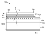
도 1은 RSC(108) 및 LED(102)를 겸비하고 있는 예시적인 디바이스(100)를 나타내고 있다. LED는 LED 기판(106) 상에 LED 반도체층(104) - 때때로 에피층(epilayer)이라고 함 - 의 적층물을 가진다. 층(104)은 p-형 및 n-형 접합부 층, 발광층(전형적으로 양자 우물을 포함함), 완충제 층, 및 상부판 층을 포함할 수 있다. 층(104)은 선택적인 접합층(116)을 통해 LED 기판(106)에 부착될 수 있다. LED는 상부면(112) 및 하부면을 가지고 있고, 상부면은 상부면이 편평한 경우와 비교하여 LED로부터의 광의 추출을 증가시키도록 텍스처링되어 있다. 도시된 바와 같이, 이들 상부면과 하부면 상에 전극(118, 120)이 제공될 수 있다. 이들 전극을 통해 적당한 전원에 연결될 때, LED는 청색 또는 자외선(UV) 광에 대응할 수 있는 제1 파장 λ1의 광을 방출한다. 이 LED 광의 일부는 RSC(108)에 들어가고 그곳에서 흡수된다.1 shows an
RSC(108)는 접합층(110)을 통해 LED의 상부면(112)에 부착되어 있다. RSC는 상부면 및 하부면(122, 124)을 가지며, 이 때 LED로부터의 펌프 광은 하부면(124)을 통해 들어간다. RSC는 또한 양자 우물 구조물(114) - 이 구조물의 일부분에서의 밴드 갭은 LED(102)에 의해 방출되는 펌프 광의 적어도 일부가 흡수되도록 선택되게 설계되어 있음- 을 포함한다. 펌프 광의 흡수에 의해 발생되는 전하 캐리어(charge carrier)는 보다 작은 밴드 갭을 갖는 구조물의 다른 부분 - 즉, 양자 우물 층 - 내로 이동하고, 여기에서 캐리어는 재결합하여 보다 긴 파장의 광을 발생한다. 이것이 도 1에서 제2 파장 λ2의 재방출된 광 - 이는 RSC(108) 내로부터 나와서 RSC를 빠져나가 출력 광을 제공함 - 으로 나타내어져 있다.RSC 108 is attached to
도 2는 RSC를 포함하는 예시적인 반도체층 적층물(210)을 나타내고 있다. 이 적층물은 분자 빔 에피택시(MBE)를 사용하여 인화인듐(InP) 웨이퍼 상에 성장되었다. GaInAs 완충제 층이 II-VI족 성장을 위한 표면을 준비하기 위해 InP 기판 상에서 MBE에 의해 먼저 성장되었다. 이어서, RSC에 사용되는 II-VI족 에피택셜층을 성장시키기 위해 웨이퍼가 초고진공 이송 시스템을 통해 다른 MBE 챔버로 이동되었다. 막 성장된 RSC의 상세가 도 2에 도시되어 있고, 표 1에 요약되어 있다. 이 표는 RSC와 연관된 다른 층에 대한 두께, 물질 조성, 밴드 갭, 및 층 설명을 열거하고 있다. RSC는 8개의 CdZnSe 양자 우물(230) - 각각이 2.15 eV의 천이 에너지를 가짐 - 을 포함하였다. 각각의 양자 우물(230)은 LED에 의해 방출된 청색 광을 흡수할 수 있는 2.48 eV의 밴드 갭 에너지를 갖는 CdMgZnSe 흡수체 층(232) 사이에 끼여 있었다. RSC는 또한 다양한 윈도우 층, 완충제 층 및 경사층을 포함하였다.2 shows an exemplary

이 RSC 디바이스 및 기타 RSC 디바이스에 대한 추가의 상세는 PCT 공개 WO 2009/048704(Kelley 등)에서 찾아볼 수 있다.Further details about this RSC device and other RSC devices can be found in PCT publication WO 2009/048704 (Kelley et al.).
본 출원에서 특히 관심을 끄는 것은 백색 광을 방출할 수 있는 광원이다. 어떤 경우에, 공지된 백색 광원은 청색-방출 LED와 같은 전계발광 디바이스와 제1 및 제2 RSC-기반 발광 요소를 결합함으로써 구성된다. 제1 발광 요소는, 예를 들어, 청색 광의 일부를 녹색 광으로 변환하고 나머지 청색 광을 투과시키는 녹색-방출 전위 우물을 포함할 수 있다. 제2 발광 요소는 제1 발광 요소로부터 수광하는 녹색 광 및/또는 청색 광의 일부를 적색 광으로 변환하고 나머지 청색 광 및 녹색 광을 투과시키는 전위 우물을 포함할 수 있다. (실시 형태들 중에서 특히) WO 2008/109296(Haase)에 기술되어 있는 이러한 디바이스가 실질적으로 백색인 광 출력을 제공할 수 있게 해주기 위해, 얻어지는 적색, 녹색 및 청색 광 성분이 결합된다.Of particular interest to the present application are light sources that can emit white light. In some cases, known white light sources are constructed by combining first and second RSC-based light emitting elements with an electroluminescent device, such as a blue-emitting LED. The first light emitting element may comprise, for example, a green-emitting potential well that converts some of the blue light into green light and transmits the remaining blue light. The second light emitting element can include a potential well that converts some of the green light and / or blue light received from the first light emitting element into red light and transmits the remaining blue and green light. The red, green and blue light components obtained are combined in order to enable such a device described in WO 2008/109296 (Haase), in particular among the embodiments, to provide a substantially white light output.
일부 디바이스는 픽셀화된 배열 또는 어레이를 사용하여 백색 광을 제공한다. 즉, 다수의 개별 발광 요소 - 어느 것도 자체적으로 백색 광을 방출하지 않음 - 가, 모여서 픽셀을 형성하도록, 서로 아주 근접하여 배열되어 있다. 픽셀은 전형적으로 관측 시스템의 분해능 한계 미만의 특성 치수 또는 크기를 가지며, 따라서 상이한 발광 요소로부터의 광이 관측 시스템에서 효과적으로 결합된다. 이러한 디바이스에 대한 통상적인 구성은 3개의 개별 발광 요소 - 적색(R) 광을 방출하는 것, 녹색(G) 광을 방출하는 것 및 청색(B) 광을 방출하는 것 - 가 "RGB" 픽셀을 형성하는 것이다. 어떤 이러한 디바이스의 개시에 대해 WO 2008/109296(Haase)을 다시 참조한다.Some devices use pixelated arrays or arrays to provide white light. That is, a number of individual light emitting elements, none of which emit white light on their own, are arranged in close proximity to each other so that they form a pixel. The pixels typically have a characteristic dimension or size below the resolution limit of the viewing system, so that light from different light emitting elements is effectively combined in the viewing system. A typical configuration for such a device is that three separate light emitting elements, one emitting red (R) light, one emitting green (G) light, and one emitting blue (B) light, produce "RGB" pixels. To form. See WO 2008/109296 (Haase) again for the disclosure of any such device.
또한, 본 출원에서 관심을 가지고 있는 것은 백색 광을 방출할 수 있을 뿐만 아니라 출력의 겉보기 색(apparent color)을 변경 또는 조정할 수 있는 광원이다. 예를 들어, 어떤 경우에, "시원한" 백색이 요망될 수 있는 반면, 다른 경우에, "따뜻한" 백색이 요망될 수 있다. 백색의 주어진 "색조(shade)"가 종래의 CIE 색도 다이어그램 상에 (x,y) 색 좌표로서 표시될 수 있고, 기술 분야의 당업자라면 잘 알고 있는 바와 같이 색 온도에 의해 특징지워질 수 있다.Also of interest in this application are light sources that can emit white light as well as change or adjust the apparent color of the output. For example, in some cases, "cool" white may be desired, while in other cases, "warm" white may be desired. A given "shade" of white can be represented as (x, y) color coordinates on a conventional CIE chromaticity diagram and can be characterized by color temperature as is well known to those skilled in the art.
예를 들어, 미국 특허 제7,387,405호(Ducharme 등)는 조정가능한 색 온도를 제공하는 조명 시스템을 기술하고 있다. 한가지 이러한 조명 시스템은 청색 방출 LED를 황색 인광체의 층과 결합시켜 구성되는 다수의 광원을 사용한다. 청색 광의 일부는 인광체에 의해 흡수되어 황색 광으로서 재방출되고, 청색 광의 일부는 인광체 층을 통과한다. 투과된 청색 광은 재방출된 황색 광과 결합하여, 공칭 백색 광으로서 인지되는 전체 출력 스펙트럼을 갖는 출력 빔을 생성한다. 인광체 층 특성 및/또는 기타 설계 상세에서의 디바이스간 변동은 출력 스펙트럼에서의 디바이스간 차이 및 인지된 색에서의 대응하는 차이를 야기하며, 어떤 LED/인광체 디바이스는 "시원한" 백색을 제공하고 다른 LED/인광체 디바이스는 "따뜻한" 백색을 제공한다. '405 특허에서 어떤 상용 LED/인광체 디바이스는 19727℃(20,000 켈빈 온도(20,000K)의 색 온도를 나타내는 반면, 다른 LED/인광체 디바이스는 5477℃(5750K)의 색 온도를 나타낸다고 보고하고 있다. '405 특허에서, 또한 이들 LED/인광체 디바이스 중 하나가 색 온도를 제어할 수 없고 원하는 색 온도 범위를 갖는 시스템이 하나의 디바이스만으로 생성될 수 없다는 것도 보고하고 있다. '405 특허는 2개의 이러한 LED/인광체 디바이스가 디바이스의 색 온도를 천이시키는 광학 장파장 투과 필터(optical long-pass filter)(장파장 광만이 통과할 수 있게 해주도록 착색된 투명한 유리 또는 플라스틱)와 결합되고 이어서 특정의 제3 LED(Agilent HLMP-EL 18 호박색 LED)가 이들 필터 기능이 있는(filtered) LED/인광체 디바이스에 추가되어 조정가능한 색 온도를 갖는 3-LED 실시 형태를 제공하는 실시 형태에 대해 계속 기술하고 있다.For example, US Pat. No. 7,387,405 (Ducharme et al.) Describes an illumination system that provides an adjustable color temperature. One such lighting system uses multiple light sources constructed by combining a blue emitting LED with a layer of yellow phosphor. Some of the blue light is absorbed by the phosphor and re-emitted as yellow light, and some of the blue light passes through the phosphor layer. The transmitted blue light combines with the re-emitted yellow light to produce an output beam with the full output spectrum perceived as nominal white light. Inter-device variations in phosphor layer properties and / or other design details result in inter-device differences in the output spectrum and corresponding differences in perceived colors, with some LEDs / phosphor devices providing "cool" white and other LEDs. The phosphor device provides a "warm" white color. The '405 patent reports that some commercial LED / phosphor devices exhibit a color temperature of 19727 ° C. (20,000 Kelvin temperature (20,000 K), while other LED / phosphor devices exhibit a color temperature of 5477 ° C. (5750K). The patent also reports that one of these LED / phosphor devices cannot control the color temperature and that a system with the desired color temperature range cannot be created with only one device.The '405 patent reports two such LED / phosphor. The device is combined with an optical long-pass filter (transparent glass or plastic colored to allow only long-wavelength light to pass through), which then changes the color temperature of the device, followed by a specific third LED (Agilent HLMP- EL 18 amber LEDs) have been added to these filtered LED / phosphor devices to provide a 3-LED embodiment with adjustable color temperature. Technology has continued for the time form.
본 출원은, 그 중에서도, 제1 및 제2 발광 요소를 포함하는 고체 조명 디바이스를 개시하고 있다. 제1 발광 요소는 제1 스펙트럼 분포을 가지는 광을 방출하도록 구성되어 있고, 제2 발광 요소는 제2 스펙트럼 분포을 가지는 광을 방출하도록 구성되어 있다. 제1 발광 요소는 제1 펌프 광을 방출하는 제1 전계발광 요소(electroluminescent element), 및 제1 펌프 광(pump light)의 적어도 일부를 제1 재방출된 광 성분으로 변환하는 제1 광 변환 요소를 포함한다. 제2 발광 요소는 제2 펌프 광을 방출하는 제2 전계발광 요소, 및 제2 펌프 광의 적어도 일부를 제2 재방출된 광 성분으로 변환하는 제2 광 변환 요소를 포함한다. 제1 및 제2 광 변환 요소 중 적어도 하나는 제1 전위 우물을 포함하는 제1 반도체 적층물을 포함한다. 제1 및 제2 발광 요소는 제1 및 제2 발광 요소에 의해 방출된 광이 결합되어 디바이스 출력을 제공하도록 배치되어 있다.The present application discloses, among other things, solid state lighting devices comprising first and second light emitting elements. The first light emitting element is configured to emit light having a first spectral distribution, and the second light emitting element is configured to emit light having a second spectral distribution. The first light emitting element includes a first electroluminescent element that emits first pump light, and a first light conversion element that converts at least a portion of the first pump light into a first re-emitted light component. It includes. The second light emitting element includes a second electroluminescent element that emits a second pump light, and a second light conversion element that converts at least a portion of the second pump light into a second re-emitted light component. At least one of the first and second light conversion elements includes a first semiconductor stack comprising a first potential well. The first and second light emitting elements are arranged to combine the light emitted by the first and second light emitting elements to provide device output.
바람직하게는, 제1 및 제2 스펙트럼 분포는, 각각, 표준 CIE (x,y) 색 좌표 다이어그램에서 라인 세그먼트를 정의하는 제1 및 제2 종점에 의해 표현될 수 있다. 라인 세그먼트는 제1 발광 요소에 의해 방출된 광 및 제2 발광 요소에 의해 방출된 광의 상이한 상대적 양에 대한 가능한 디바이스 출력의 범위를 나타낼 수 있다. 예시적인 실시 형태에서, 라인 세그먼트는 또한 적어도 주어진 범위에 걸쳐 "플랑키안 궤적(Planckian locus)"에 가깝다. 기술 분야의 당업자라면, 플랑키안 궤적이 통상 켈빈 온도로 측정되는 일정 범위의 온도 - 이 온도를 "색 온도" Tc라고 함 - 에 걸쳐 이상적인 흑체 광원의 색상을 말한다는 것을 잘 알 것이다. 따라서, 라인 세그먼트는, 예를 들어, 2727℃(3000K)부터 4727℃(5000K)까지, 또는 2227℃(2500K)부터 4727℃(5000K)까지의 색 온도 범위에 걸쳐 플랑키안 궤적에 가까울 수 있다. 이러한 색 온도 범위에 걸쳐, 라인 세그먼트가 CIE (x,y) 평면에서 0.04 미만 또는 0.02 미만의 거리만큼 플랑키안 궤적으로부터 벗어날 수 있다.Preferably, the first and second spectral distributions may be represented by first and second endpoints defining line segments in a standard CIE (x, y) color coordinate diagram, respectively. The line segment may represent a range of possible device outputs for different relative amounts of light emitted by the first light emitting element and light emitted by the second light emitting element. In an exemplary embodiment, the line segment is also close to the "Planckian locus" over at least the given range. Those skilled in the art will appreciate that the Planckian trajectory refers to the color of the ideal blackbody light source over a range of temperatures, commonly referred to as Kelvin temperatures, referred to as "color temperature" T c . Thus, the line segment may be close to the Planckian trajectory, for example, over a color temperature range from 2727 ° C (3000K) to 4727 ° C (5000K), or from 2227 ° C (2500K) to 4727 ° C (5000K). Over this color temperature range, line segments may deviate from Planckian trajectories by a distance of less than 0.04 or less than 0.02 in the CIE (x, y) plane.
게다가, 예시적인 실시 형태에서, 제1 및 제2 발광 요소는 양호한 "연색" 특성을 나타내는 디바이스 출력을 생성한다. 기술 분야의 당업자라면 이하에서 더 논의되는 연색 지수를 잘 알고 있을 것이다. 디바이스 출력은 바람직하게는 적어도 60, 또는 적어도 70, 또는 적어도 80의 연색 지수를 나타낼 수 있다. 게다가, 이러한 연색 지수 값은 디바이스 출력의 색 온도 범위에 걸쳐, 예를 들어, 2727℃(3000K)부터 4727℃(5000K)까지, 또는 2227℃(2500K)부터 4727℃(5000K)까지의 색 온도 범위에 걸쳐 유지될 수 있다.In addition, in the exemplary embodiment, the first and second light emitting elements produce device outputs that exhibit good "color rendering" characteristics. Those skilled in the art will be familiar with the color rendering index, discussed further below. The device output may preferably exhibit a color rendering index of at least 60, or at least 70, or at least 80. In addition, such color rendering index values can range over the color temperature range of the device output, for example, from 2727 ° C (3000K) to 4727 ° C (5000K), or from 2227 ° C (2500K) to 4727 ° C (5000K). Can be maintained over.
일부 실시 형태에서, 제1 및 제2 펌프 광 각각은 350 ㎚부터 500 ㎚까지의 범위에서 피크 파장을 나타낸다. 예를 들어, 이들 펌프 광 각각은 UV, 보라색 및/또는 청색 광을 포함할 수 있다. 일부 실시 형태에서, 제1 펌프 광의 피크 파장은 제2 펌프 광의 피크 파장과 실질적으로 동일할 수 있다. 제1 및 제2 전계발광 광원은 단일 반도체 요소의 상이한 부분, 예를 들어, 개별적으로 전기적으로 어드레싱가능한 LED 또는 유사한 반도체 디바이스의 상이한 영역을 포함할 수 있다. 대안적으로, 제1 및 제2 전계발광 광원이 개별 반도체 요소를 포함할 수 있다.In some embodiments, each of the first and second pump lights exhibits a peak wavelength in the range from 350 nm to 500 nm. For example, each of these pump lights may comprise UV, purple and / or blue light. In some embodiments, the peak wavelength of the first pump light can be substantially the same as the peak wavelength of the second pump light. The first and second electroluminescent light sources can comprise different portions of a single semiconductor element, eg, different regions of an individually electrically addressable LED or similar semiconductor device. Alternatively, the first and second electroluminescent light sources can comprise separate semiconductor elements.
어떤 경우에, 제1 광 변환 요소는 인광체를 포함할 수 있고, 제2 광 변환 요소는 제1 전위 우물을 포함하는 제1 반도체 적층물을 포함할 수 있다. 다른 경우에, 제1 광 변환 요소는 제1 반도체 적층물을 포함할 수 있고, 제2 광 변환 요소는 제2 전위 우물을 포함하는 제2 반도체 적층물을 포함할 수 있다. 어떤 경우에, 제1 스펙트럼 분포는 시안색에 의해 특징지워질 수 있고, 제2 스펙트럼 분포는 호박색에 의해 특징지워질 수 있다. 어떤 경우에, 제1 스펙트럼 분포는 400 ㎚와 500 ㎚ 사이에서 피크 방출을 갖는 제1 방출 대역 및 500 ㎚와 600 ㎚ 사이에서 피크 방출을 갖는 제2 방출 대역을 포함할 수 있거나 본질적으로 이들 방출 대역으로 이루어져 있을 수 있다. 제2 스펙트럼 분포는, 예를 들어, 500 ㎚와 600 ㎚ 사이에서 피크 방출을 갖는 제3 방출 대역 및 600 ㎚와 700 ㎚ 사이에서 피크 방출을 갖는 제4 방출 대역을 포함할 수 있거나 본질적으로 이들 방출 대역으로 이루어져 있을 수 있다. 제1 및 제2 스펙트럼 분포는, 개별적으로든지 결합되든지 간에, 적어도 10 ㎚만큼 서로 상이한 피크 파장을 나타낼 수 있다.In some cases, the first light conversion element may comprise a phosphor and the second light conversion element may comprise a first semiconductor stack comprising a first potential well. In other cases, the first light conversion element may comprise a first semiconductor stack and the second light conversion element may comprise a second semiconductor stack comprising a second potential well. In some cases, the first spectral distribution may be characterized by cyan and the second spectral distribution may be characterized by amber. In some cases, the first spectral distribution may include or consist essentially of a first emission band having a peak emission between 400 nm and 500 nm and a second emission band having a peak emission between 500 nm and 600 nm. It may consist of. The second spectral distribution may comprise or consist essentially of, for example, a third emission band having a peak emission between 500 nm and 600 nm and a fourth emission band having a peak emission between 600 nm and 700 nm. It may consist of bands. The first and second spectral distributions, whether individually or combined, can exhibit peak wavelengths that differ from each other by at least 10 nm.
관련 방법, 시스템 및 물품이 또한 논의된다.Related methods, systems and articles are also discussed.
본 출원의 이들 태양 및 다른 태양이 이하의 상세한 설명으로부터 명백해질 것이다. 그러나, 어떠한 경우에도 상기 개요는 청구된 요지에 대한 제한으로서 해석되어서는 안되며, 그 요지는 절차의 수행 동안 보정될 수 있는 첨부된 특허청구범위에 의해서만 한정된다.These and other aspects of the present application will be apparent from the detailed description below. In no event, however, should the above summary be interpreted as a limitation on the claimed subject matter, which subject matter is defined only by the appended claims, which may be amended during the performance of the procedure.
도 1은 LED/RSC 결합 디바이스의 개략 측면도.
도 2는 RSC를 포함하는 예시적인 반도체층 적층물의 개략 측면도.
도 3은 조명 디바이스를 나타내는 라인 세그먼트가 표시되어 있는 CIE 색도 다이어그램.
도 3a 및 도 3b는 도 3의 조명 디바이스의 2개의 성분의 방출 스펙트럼의 그래프.
도 4는 다른 조명 디바이스를 나타내는 라인 세그먼트가 표시되어 있는 CIE 색도 다이어그램.
도 4a 및 도 4b는 도 4의 조명 디바이스의 2개의 성분의 방출 스펙트럼의 그래프.
도 5는 도 3 및 도 4의 조명 디바이스에 대한 색 온도의 함수로서 계산된 연색 지수(CRI)의 그래프.
도 6 및 도 7은 추가의 조명 디바이스의 개략 단면도.
도 8 및 도 9는 추가의 조명 디바이스의 개략 평면도.
도 10은 조명 디바이스의 제1 및 제2 발광 요소에 의해 방출된 광의 일부분을 자동으로 조정하는 데 사용될 수 있는 회로를 나타낸 도면.
도 11a는 도 10의 회로에 있는 각자의 다이오드를 통해 흐르는 전류(각자의 다이오드에 의해 방출되는 광의 양을 나타냄)를 인가된 신호의 전위 또는 전압의 함수로서 나타낸 그래프.
도 11b는 도 11a의 그래프와 유사한 것으로서, 응답을 총 다이오드 전류의 함수로서 나타낸 그래프.
이들 도면에서, 동일한 도면 부호는 동일한 요소를 가리킨다.1 is a schematic side view of an LED / RSC combining device.
2 is a schematic side view of an exemplary semiconductor layer stack including RSC.
3 is a CIE chromaticity diagram showing line segments representing lighting devices.
3A and 3B are graphs of emission spectra of two components of the lighting device of FIG. 3.
4 is a CIE chromaticity diagram with line segments representing different lighting devices.
4A and 4B are graphs of emission spectra of two components of the lighting device of FIG. 4.
5 is a graph of color rendering index (CRI) calculated as a function of color temperature for the lighting device of FIGS. 3 and 4.
6 and 7 show schematic cross-sectional views of additional lighting devices.
8 and 9 are schematic plan views of further lighting devices.
10 shows a circuit that can be used to automatically adjust the portion of light emitted by the first and second light emitting elements of the lighting device.
FIG. 11A is a graph showing the current flowing through each diode in the circuit of FIG. 10 (indicating the amount of light emitted by each diode) as a function of the potential or voltage of the applied signal. FIG.
FIG. 11B is similar to the graph of FIG. 11A, showing the response as a function of total diode current. FIG.
In these figures, like reference numerals refer to like elements.
이상에 요약되어 있는 바와 같이, 본 출원은 (그 중에서도 특히) 제1 발광 요소로부터 방출된 광이 제2 발광 요소로부터 방출된 광과 결합되어 디바이스 광 출력을 제공할 수 있는 조명 디바이스를 기술하고 있다. 디바이스 광 출력의 색상(예컨대, 색 온도)을 조정하기 위해 이들 제1 및 제2 발광 요소로부터의 광의 상대적인 양이 조정될 수 있다. 제1 및 제2 발광 요소에 의해 방출된 광의 스펙트럼 분포(스펙트럼)이 적절히 선택되는 경우, 디바이스 광 출력의 인지된 색상이 주어진 온도 Tc에서 이상적인 흑체 광원의 색상에 가깝도록 할 수 있다. 게다가, 얻어지는 조정된 색상(들)이 또한 상이한 색 온도(들) Tc에서 흑체 광원의 색상에 가깝게 되도록, 디바이스 광 출력의 색상에 대한 조정이 행해질 수 있다(제1 및 제2 발광 요소로부터의 광의 상대적인 양의 조정을 통해 행해짐).As summarized above, the present application describes an illumination device in which light emitted from a first light emitting element (particularly) may be combined with light emitted from a second light emitting element to provide a device light output. . The relative amounts of light from these first and second light emitting elements can be adjusted to adjust the color (eg, color temperature) of the device light output. If the spectral distribution (spectrum) of the light emitted by the first and second light emitting elements is appropriately selected, then the perceived color of the device light output can be made close to the color of the ideal blackbody light source at a given temperature T c . In addition, adjustments can be made to the color of the device light output so that the adjusted color (s) obtained are also close to the color of the blackbody light source at different color temperature (s) T c (from the first and second light emitting elements). By adjusting the relative amount of light).
이들 바람직한 색 온도 특성을 만족시킬 뿐만 아니라 양호한 연색 성능을 제공할 수도 있는 제1 및 제2 발광 요소에 대한 스펙트럼이 용이하게 얻어질 수 있다는 것을 알았다. 예를 들어, 적어도 60, 또는 적어도 70, 또는 적어도 80의 연색 지수가 달성될 수 있는 모델링이 설명되어 있다. 게다가, 이러한 연색 지수는 디바이스 광 출력의 넓은 색 조정 범위에 걸쳐, 예를 들어, 2727℃(3000K)부터 4727℃(5000K)까지, 또는 2227℃(2500K)부터 4727℃(5000K)까지의 색 온도 범위에 걸쳐 유지될 수 있다.It has been found that the spectra for the first and second light emitting elements that can not only satisfy these desirable color temperature characteristics but also provide good color rendering performance can be easily obtained. For example, modeling has been described in which a color rendering index of at least 60, or at least 70, or at least 80 can be achieved. In addition, these color rendering indices can be used over a wide color adjustment range of the device light output, for example, from 2727 ° C (3000K) to 4727 ° C (5000K), or from 2227 ° C (2500K) to 4727 ° C (5000K). Can be maintained over a range.
펌프 광을 방출하는 LED 등과 같은 적당한 전계발광 광원과 펌프 광의 적어도 일부를 재방출된 광으로 변환하는 RSC, 인광체 등과 같은 광 변환 요소의 조합을 사용하여 이러한 디바이스가 제조될 수 있다. 디바이스 자체 및 다양한 주요 구성요소가 이하에서 더 기술된다. 그렇지만, 이러한 설명을 시작하기 전에, 디바이스의 고유의 광학 특성 - 색 표시(color appearance) 특성(그의 조정을 포함함) 및 연색 특성을 포함함 - 에 대해 먼저 기술할 것이다. 이를 위해, CIE 색도 다이어그램을 사용한다.Such a device can be manufactured using a combination of suitable electroluminescent light sources, such as LEDs that emit pump light, and light conversion elements, such as RSC, phosphors, etc., that convert at least some of the pump light into re-emitted light. The device itself and various major components are further described below. However, before beginning this description, the inherent optical properties of the device, including color appearance properties (including their adjustments) and color rendering properties, will be described first. To do this, use a CIE chromaticity diagram.
기술 분야의 당업자라면 인지된 색상을 특성 파악하고 정량화하는 데 사용되는 도구 또는 표준 - 상세하게는, CIE[Commission International de l'Eclairage(International Commission on Lighting)]에 의해 발표된 공지의 1931 CIE 색도 다이어그램 - 을 잘 알 것이다. 광원 또는 물품의 색상(또는 "색도" 또는 "색도 좌표")이 CIE 1931 표준 표색계를 사용하여 CIE 색도 다이어그램 상의 하나 이상의 색도 좌표 (x,y)로 표현되는 지점 또는 영역에 의해 정확하게 측정되거나 지정될 수 있다.Tools or standards used by those skilled in the art to characterize and quantify perceived colors—in particular, the known 1931 CIE chromaticity diagram published by the Commission International de l'Eclairage (International Commission on Lighting). -You will know well. The color (or "chromatic" or "chromatic coordinate") of a light source or article may be accurately measured or specified by a point or area represented by one or more chromaticity coordinates (x, y) on a CIE chromaticity diagram using the CIE 1931 standard colorimetric system. Can be.
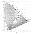
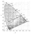
이러한 색도 다이어그램이 도 3에 도시되어 있다. 기술 분야의 당업자라면 전술한 플랑키안 궤적인 곡선(310)을 잘 알 것이다. 다이어그램 상의 다른 특징은 조명 디바이스의 특정 실시 형태 또는 실시 형태들을 나타낸 것이다.This chromaticity diagram is shown in FIG. 3. Those skilled in the art will be familiar with the
상세하게는, 지점 P1 및 P2는, 각각, 제1 및 제2 발광 요소에 의해 방출되는 광의 색상을 나타낸다. 이들 색상은 특별히 점 P1과 P2를 연결하는 라인 세그먼트(312)가 그의 상당 부분에 걸쳐 플랑키안 궤적(310)에 아주 가깝도록 선택된다. 도시된 실시 형태에서, 라인 세그먼트(312)는 2727℃(3000K)부터 4727℃(5000K)까지의 (플랑키안 궤적에 대한) 색 온도 범위에 걸쳐 CIE (x,y) 평면 상에서 0.005 이하의 거리만큼 플랑키안 궤적(310)으로부터 벗어나 있다. 2227℃(2500K)부터 4727℃(5000K)까지의 넓은 색 온도 범위에 걸쳐, 라인 세그먼트(312)는 CIE (x,y) 평면에서 0.01 이하의 거리만큼 플랑키안 궤적(310)으로부터 벗어나 있다.Specifically, the points P1 and P2 represent the color of the light emitted by the first and second light emitting elements, respectively. These colors are chosen in particular so that the
라인 세그먼트(312)가 제1 발광 요소에 의해 방출된 광(P1으로 표현됨)과 제2 발광 요소에 의해 방출된 광(P2로 표현됨)의 선형 조합으로 이루어진 출력을 갖는 조명 디바이스에 대한 모든 가능한 광 출력의 집합을 나타낸다는 것을 염두에 두어야 한다. 따라서, 예를 들어, P1으로 표현된 광과 P2로 표현된 광을 똑같이 포함하는 광 출력을 갖는 조명 디바이스는 라인 세그먼트(312)를 양분하는 지점에 의해 표현된다. 지점 P1의 광의 비율이 증가되면, 디바이스 출력 지점은 라인 세그먼트(312)를 따라 지점 P1 쪽으로 이동한다. 그 대신에 지점 P2의 광의 비율이 증가되면, 디바이스 출력 지점은 라인 세그먼트(312)를 따라 지점 P2 쪽으로 이동한다. 따라서, 제1 및 제2 발광 요소에 의해 방출되는 광의 상대적 양을 조정함으로써, 디바이스 출력의 색상이 변경되거나 조정될 수 있다.All possible light for the lighting device with the
지점 P1, P2에 의해 표현되는 색상은 전계발광 광원과 광 변환 요소의 많은 상이한 조합에 의해 달성될 수 있는데, 그 이유는 CIE 색도 다이어그램 상에서의 임의의 특정의 색 좌표가 실질적으로 서로 상이할 수 있는 다수의 광 스펙트럼과 연관될 수 있기 때문이다. 본 개시 내용은 모든 이러한 조합을 포괄한다. 그렇지만, 적은 수의 개별 스펙트럼 피크 - 예를 들어, 하나의 지점 또는 각각의 지점에 대한 정확히 2개의 개별 스펙트럼 피크, 또는 하나의 지점 또는 각각의 지점에 대한 정확히 3개의 개별 스펙트럼 피크 - 의 조합을 사용하여 지점 P1, P2 중 하나 또는 둘다를 생성하는 것이 유리하다는 것을 알았다.The color represented by points P1, P2 can be achieved by many different combinations of electroluminescent light sources and light conversion elements, since any particular color coordinates on the CIE chromaticity diagram can be substantially different from each other. As it can be associated with multiple light spectra. The present disclosure encompasses all such combinations. However, using a combination of a small number of individual spectral peaks—for example, exactly two individual spectral peaks for one point or each point, or exactly three individual spectral peaks for one point or each point— It has been found to be advantageous to create one or both of points P1, P2.
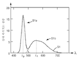
도시된 실시 형태에서, 지점 P1으로 표현된 광은 2개의 개별 스펙트럼 피크 - 이들 중 하나는 지점 P1a로 표현되고 이들 중 다른 하나는 지점 P1b로 표현됨 - 의 조합이다. 지점 P1a로 표현되는 광은 약 465 ㎚의 피크 파장 및, 예를 들어, 50 ㎚ 미만, 또는 30 ㎚ 미만, 예를 들어, 25 ㎚의 FWHM(full-width at half-maximum) 값으로 측정되는 스펙트럼 폭을 가지는 청색 LED에 의해 방출된 광을 나타낸다. 지점 P1b로 표현되는 광은, 인광체가 청색 또는 기타 단파장 광으로 여기될 때, 세륨-도핑된 이트륨 알루미늄 가닛(YAG:Ce)과 같은 황색 인광체로부터 재방출되는 광을 나타낸다. 이러한 재방출된 광은 약 550 ㎚의 피크 파장 및 150 n 미만 또는 100 ㎚ 미만의 FWHM 스펙트럼 폭을 가질 수 있다. 도 3a는 지점 P1, P1a 및 P1b을 예시하고 있는 스펙트럼 S1을 나타낸 것이다. 상세하게는, 스펙트럼 S1은 제1 스펙트럼 피크 S1a 및 (부분적으로 중복하는) 제2 스펙트럼 피크 S1b의 혼합 또는 조합이다. 제1 스펙트럼 피크 S1a는 청색 LED에 의해 방출된 청색 펌프 광 - 이 광의 색상이 지점 P1a로 표현됨 - 을 나타내는 피크 파장 λp 및 스펙트럼 폭을 가진다. 제2 스펙트럼 피크 S1b는 황색 인광체로부터 재방출된 광 - 이 광의 색상이 지점 P1b로 표현됨 - 을 나타내는 피크 파장 λ1 및 스펙트럼 폭을 가진다. 적당한 상대적 양 또는 비율로 2개의 스펙트럼 피크 S1a, S1b를 조합하면 결과 스펙트럼 S1 - 이 스펙트럼의 색상이 지점 P1으로 표현됨 - 을 생성한다. 도시된 실시 형태에서, 스펙트럼 피크 S1b의 적분된 세기가 스펙트럼 피크 S1a의 적분된 세기의 약 2.3배이도록 비율이 선택되고, 그 결과 공칭상 백색인 지점 P1에 대한 색상이 얻어진다. 청색 광-방출 전계발광 광원 - 이 광원 상에 황색 인광체 물질의 층이 도포되어 있음 - 을 포함하는 제1 발광 요소에 의해 스펙트럼 S1을 가지는 광이 생성될 수 있고, 여기서 인광체 층은 청색 펌프 광의 적절한 부분을 투과시키기 위해 적절히 얇거나 다른 방식으로 설계되어 있다.In the embodiment shown, the light represented by point P1 is a combination of two separate spectral peaks, one of which is represented by point P1a and the other of which is represented by point P1b. The light represented by the point P1a is measured by a peak wavelength of about 465 nm and a full-width at half-maximum (FWHM) value of, for example, less than 50 nm, or less than 30 nm, for example 25 nm. Represents light emitted by a blue LED having a width. Light represented by point P1b represents light that is re-emitted from a yellow phosphor, such as cerium-doped yttrium aluminum garnet (YAG: Ce) when the phosphor is excited with blue or other short wavelength light. Such re-emitting light may have a peak wavelength of about 550 nm and an FWHM spectral width of less than 150 n or less than 100 nm. 3A shows the spectrum S1 illustrating the points P1, P1a and P1b. Specifically, the spectrum S1 is a mixture or combination of the first spectral peak S1a and the (partially overlapping) second spectral peak S1b. The first spectral peak Sla has a spectral width and a peak wavelength λ p which represents the blue pump light emitted by the blue LED, the color of which is represented by the point Pla. The second spectral peak S1b has a peak wavelength λ 1 and a spectral width indicating light re-emitted from the yellow phosphor, the color of which is represented by the point P1b. Combining the two spectral peaks S1a, S1b in the appropriate relative amount or ratio produces the resulting spectrum S1, where the color of this spectrum is represented by point P1. In the illustrated embodiment, the ratio is selected such that the integrated intensity of spectral peak S1b is about 2.3 times the integrated intensity of spectral peak S1a, resulting in a color for point P1 that is nominally white. Light having spectrum S1 can be produced by a first light emitting element comprising a blue light-emitting electroluminescent light source, on which the layer of yellow phosphor material is applied, wherein the phosphor layer is suitable for the blue pump light. It is suitably thin or otherwise designed to penetrate the part.
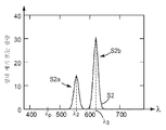
이와 유사하게, 도시된 실시 형태에서, 지점 P2로 표현된 광도 역시 2개의 개별 스펙트럼 피크 - 이들 중 하나는 지점 P2a로 표현되고 이들 중 다른 하나는 지점 P2b로 표현됨 - 의 조합이다. 지점 P2a로 표현되는 광은, RSC가 청색 또는 기타 단파장 펌프 광에 의해 여기될 때, 도 1 및 도 2와 관련하여 기술된 것과 같은 재방출 반도체 구조체(RSC)의 하나 이상의 전위 우물에 의해 재방출된 광을 나타낸다. 이 실시 형태에서, 이러한 전위 우물(들)은 약 555 ㎚의 피크 파장 및 50 ㎚ 미만, 또는 30 ㎚ 미만, 예를 들어, 18 ㎚의 FWHM 스펙트럼 폭을 가지는 녹색 광을 재방출하도록 설계되어 있다. 지점 P2b로 표현되는 광은 또한 단파장 펌프 광에 의해 조명될 때 RSC의 하나 이상의 전위 우물로부터 재방출되는 광을 나타내지만, 지점 P2b와 연관된 전위 우물(들)은 지점 P2a와 연관된 전위 우물(들)과 다르다. 지점 P2b와 연관된 전위 우물(들)은 약 620 ㎚의 피크 파장 및 50 ㎚ 미만, 또는 30 ㎚ 미만, 예를 들어, 18 ㎚의 FWHM 스펙트럼 폭을 가지는 적색 광을 재방출하도록 설계되어 있다. 적당한 상대적 양 또는 비율로 2개의 스펙트럼 피크 S2a, S2b를 조합하면 결과 스펙트럼 S2 - 이 스펙트럼의 색상이 지점 P2로 표현됨 - 를 생성한다. 도시된 실시 형태에서, 스펙트럼 피크 S2b의 적분된 세기가 스펙트럼 피크 S2a의 적분된 세기의 약 2배이도록 비율이 선택되고, 그 결과 실질적으로 호박색인 지점 P2에 대한 색상이 얻어진다. 스펙트럼 S2를 가지는 광이 청색 또는 기타 단파장 펌프 광-방출 전계발광 광원 - 이 광원 상에 적절히 설계된 RSC가 도포되어 있음 - 을 포함하는 제1 발광 요소에 의해 생성될 수 있고, 여기서 RSC는 펌프 광을 실질적으로 차단하고(스펙트럼 S2에서의 펌프 파장 λp에서 어떤 상당한 세기도 없음에 주목할 것) 스펙트럼 피크 S2a를 가지는 광과 스펙트럼 피크 S2b를 가지는 광을 정확한 비율로 방출하도록 설계되어 있다. 펌프 광을 실질적으로 차단하기 위해, RSC는 RSC의 임의의 흡수층(들)에 의해 흡수되지 않는 파장 λp의 펌프 광원에 의해 공급되는 단파장 광은 실질적으로 전부 흡수하지만 전위 우물(들)로부터 나오는 재방출된 광은 대부분 투과시키는 광 필터링 층을 포함할 수 있고, 이 층은 때때로 "시안 차단체(cyan blocker)"라고 한다. 이와 관련하여, 2009년 5월 5일자로 출원된, 발명의 명칭이 "Re-Emitting Semiconductor Carrier Devices For Use With LEDs and Methods of Manufacture(LED에서 사용되는 재방출 반도체 캐리어 디바이스 및 제조 방법)"인 동시 계류 중인 미국 특허 출원 제61/175,636호(대리인 사건 번호 65435US002)를 참조하며, 이 미국 출원은 참조 문헌으로서 본 명세서에 포함된다. 완성된 디바이스에서, 이러한 층은 펌프 광원과 마주하는 측면의 반대쪽에 있는 RSC의 측면 상에, 즉 활성 영역 및 특히 활성 영역의 전위 우물이 펌프 광원과 광 필터링층/시안 차단체 사이에 배치되도록 포함될 수 있다.Similarly, in the illustrated embodiment, the light intensity represented by point P2 is also a combination of two separate spectral peaks, one of which is represented by point P2a and the other of which is represented by point P2b. The light represented by point P2a is re-emitted by one or more potential wells of the re-emitting semiconductor structure (RSC) as described in connection with FIGS. 1 and 2 when the RSC is excited by blue or other short wavelength pump light. Indicated light. In this embodiment, such potential well (s) are designed to re-emit green light having a peak wavelength of about 555 nm and an FWHM spectral width of less than 50 nm, or less than 30 nm, for example 18 nm. The light represented by point P2b also represents light re-emitted from one or more potential wells of the RSC when illuminated by short wavelength pump light, but the potential well (s) associated with point P2b is the potential well (s) associated with point P2a. Is different. The potential well (s) associated with point P2b is designed to re-emit red light having a peak wavelength of about 620 nm and an FWHM spectral width of less than 50 nm, or less than 30 nm, for example 18 nm. Combining the two spectral peaks S2a, S2b in an appropriate relative amount or ratio yields the resulting spectrum S2, where the color of this spectrum is represented by point P2. In the embodiment shown, the ratio is selected such that the integrated intensity of spectral peak S2b is about twice the integrated intensity of spectral peak S2a, resulting in a color for point P2 that is substantially amber. Light having a spectrum S2 may be generated by a first light emitting element comprising a blue or other short wavelength pump light-emitting electroluminescent light source, with a suitably designed RSC applied on the light source, wherein the RSC generates the pump light. It is designed to block substantially (no noticeable intensity at the pump wavelength λ p at spectrum S2) and to emit light with spectral peak S2a and light with spectral peak S2b at the correct ratio. To substantially block pump light, RSC absorbs substantially all of the short wavelength light supplied by the pump light source at wavelength λ p , which is not absorbed by any absorbing layer (s) of the RSC, but the ash from the potential well (s). The emitted light may comprise a light filtering layer that transmits mostly, which is sometimes referred to as a "cyan blocker." In this regard, a filed application dated May 5, 2009, entitled "Re-Emitting Semiconductor Carrier Devices For Use With LEDs and Methods of Manufacture". See pending US patent application Ser. No. 61 / 175,636 (Agent Case No. 65435US002), which is incorporated herein by reference. In the finished device, this layer is included on the side of the RSC opposite the side facing the pump light source, ie so that the potential wells of the active area and in particular the active area are arranged between the pump light source and the light filtering layer / cyan blocker. Can be.
주목할 점은, 도 3a의 상기 설명에서, 심볼 λ1이 도 1에서의 그의 의미와 얼마간 상이한 의미를 가진다는 것인데, 그 이유는 도 3a에서는 광 변환 요소로부터의 재방출된 광과 연관되어 있지만, 도 1에서는 전계발광 디바이스에 의해 발생된 펌프 광과 연관되어 있기 때문이다. 도 3b 및 도 1 둘다에서 광 변환 요소로부터의 재방출된 광과 연관되어 있는 심볼 λ2는 이들 2개의 도면에서 동일한 의미를 가질 수 있거나 얼마간 상이한 의미를 가질 수 있다.Note that in the above description of FIG. 3A, the symbol λ 1 has a meaning that is somewhat different from its meaning in FIG. 1, because in FIG. 3A associated with the re-emitted light from the light conversion element, This is because in FIG. 1 it is associated with the pump light generated by the electroluminescent device. The symbols λ 2 associated with the re-emitted light from the light conversion element in both FIGS. 3B and 1 may have the same meaning in some of these two figures or may have some different meaning.
도 3b에 도시된 스펙트럼과 유사한, 2개의 피크 파장을 포함하는 스펙트럼을 가지는 광을 동시에 방출할 수 있는 RSC를 포함하는 예시적인 반도체 적층물이 이하의 표 2에 나타내어져 있다. 이 적층물은 녹색 스펙트럼 피크를 생성하는 하나의 녹색-방출(555 ㎚) 양자 우물, 및 적색 스펙트럼 피크를 생성하는 하나의 적색-방출(620 ㎚) 양자 우물을 포함한다. 녹색 피크와 적색 피크의 상대적 세기는 원칙적으로 각자의 양자 우물과 연관되어 있는 흡수체 층의 두께에 의해 제어된다. 녹색-방출 양자 우물에 인접하여 비교적 얇은 흡수체 층을 사용함으로써, 보다 많은 펌프 광이 이들 층을 통과하고 적색-방출 양자 우물에 인접한 흡수체 층에서 흡수될 것이다. 이 결과, 녹색 광보다 더 많은 적색 광이 방출될 수 있다. 녹색 광 대 적색 광의 비가 또한 임의의 광-추출 특징부의 존재에 의해 얼마간 영향을 받을 수 있으며, 예컨대, 여기서 이러한 특징부는 시안 차단체의 외측 표면 내에 에칭되거나 그에 부착된다.An exemplary semiconductor stack including RSC capable of simultaneously emitting light having a spectrum comprising two peak wavelengths, similar to the spectrum shown in FIG. 3B, is shown in Table 2 below. This stack includes one green-emitting (555 nm) quantum well that produces a green spectral peak, and one red-emitting (620 nm) quantum well that produces a red spectral peak. The relative intensities of the green and red peaks are in principle controlled by the thickness of the absorber layer associated with the respective quantum wells. By using a relatively thin absorber layer adjacent to the green-emitting quantum wells, more pump light will pass through these layers and be absorbed in the absorber layer adjacent to the red-emitting quantum wells. As a result, more red light can be emitted than green light. The ratio of green light to red light can also be influenced in part by the presence of any light-extracting features, such as where such features are etched or attached to the outer surface of the cyan blocker.

기술 분야의 당업자라면 다양한 층에 대한 열거된 밴드 갭 에너지를 달성하기 위해 CdMgZnSe 합금의 조성을 어떻게 조정해야 하는지를 잘 알 것이다. 예를 들어, CdMgZnSe 합금의 밴드 갭 에너지는 주로 Mg 함유량에 의해 제어된다. 양자 우물의 방출 파장(또는 에너지)은 Cd/Zn 비 및 양자 우물의 정확한 두께 둘다에 의해 제어된다.Those skilled in the art will know how to adjust the composition of the CdMgZnSe alloy to achieve the listed band gap energy for the various layers. For example, the band gap energy of CdMgZnSe alloy is mainly controlled by the Mg content. The emission wavelength (or energy) of the quantum well is controlled by both the Cd / Zn ratio and the exact thickness of the quantum well.
도 3의 것과 유사한 색도 다이어그램이 도 4에 도시되어 있다. 도 4에서, 곡선(310)도 역시 전술한 플랑키안 궤적을 나타낸 것이다. 그렇지만, 도 4는 조명 디바이스의 상이한 특정의 실시 형태 또는 실시 형태들을 나타내는 도 3의 것과 상이한 기타 특징부를 포함한다.A chromaticity diagram similar to that of FIG. 3 is shown in FIG. 4. In Figure 4,
상세하게는, 지점 P3 및 P4는, 각각, 제1 및 제2 발광 요소에 의해 방출되는 광의 색상을 나타낸다. (주목할 점은, 이들 제1 및 제2 요소 중 하나 또는 둘다가 도 3과 관련하여 기술된 제1 및 제2 발광 요소와 상이할 수 있다는 것이다.) 이들 색상은 특별히 점 P3와 P4를 연결하는 라인 세그먼트(412)가 그의 상당 부분에 걸쳐 플랑키안 궤적(310)에 아주 가깝도록 선택된다. 도시된 실시 형태에서, 라인 세그먼트(412)는 2727℃(3000K)부터 4727℃(5000K)까지의 (플랑키안 궤적에 대한) 색 온도 범위에 걸쳐 CIE (x,y) 평면 상에서 0.005 이하의 거리만큼 플랑키안 궤적(310)으로부터 벗어나 있다. 2227℃(2500K)부터 4727℃(5000K)까지의 넓은 색 온도 범위에 걸쳐, 라인 세그먼트(312)는 CIE (x,y) 평면에서 0.01 이하의 거리만큼 플랑키안 궤적(310)으로부터 벗어나 있다. 일반적으로, 라인 세그먼트가 언급한 색 온도 범위에 걸쳐 CIE (x,y) 평면 상에서 0.04 이하 또는 0.02 이하의 거리만큼 플랑키안 궤적으로부터 벗어나는 것이 바람직하다.In detail, the points P3 and P4 represent the color of the light emitted by the first and second light emitting elements, respectively. (Note that one or both of these first and second elements may be different than the first and second light emitting elements described in connection with FIG. 3). These colors specifically connect points P3 and P4.
라인 세그먼트(412)가 제1 발광 요소에 의해 방출된 광(P3로 표현됨)과 제2 발광 요소에 의해 방출된 광(P4로 표현됨)의 선형 조합으로 이루어진 출력을 갖는 조명 디바이스에 대한 모든 가능한 광 출력의 집합을 나타낸다. 따라서, 예를 들어, P3로 표현된 광과 P4로 표현된 광을 똑같이 포함하는 광 출력을 갖는 조명 디바이스는 라인 세그먼트(412)를 양분하는 지점에 의해 표현된다. 지점 P3의 광의 비율이 증가되면, 디바이스 출력 지점은 라인 세그먼트(412)를 따라 지점 P3 쪽으로 이동한다. 그 대신에 지점 P4의 광의 비율이 증가되면, 디바이스 출력 지점은 라인 세그먼트(412)를 따라 지점 P4 쪽으로 이동한다. 따라서, 제1 및 제2 발광 요소에 의해 방출되는 광의 상대적 양을 조정함으로써, 디바이스 출력의 색상이 변경되거나 조정될 수 있다.All possible light for the lighting device where the
지점 P3, P4에 의해 표현되는 색상은 전계발광 광원과 광 변환 요소의 많은 상이한 조합에 의해 달성될 수 있는데, 그 이유는 CIE 색도 다이어그램 상에서의 임의의 특정의 색 좌표가 실질적으로 서로 상이할 수 있는 다수의 광 스펙트럼과 연관될 수 있기 때문이다. 본 개시 내용은 모든 이러한 조합을 포괄한다. 그렇지만, 적은 수의 개별 스펙트럼 피크 - 예를 들어, 하나의 지점 또는 각각의 지점에 대한 정확히 2개의 개별 스펙트럼 피크, 또는 하나의 지점 또는 각각의 지점에 대한 정확히 3개의 개별 스펙트럼 피크 - 의 조합을 사용하여 지점 P3, P4 중 하나 또는 둘다를 생성하는 것이 유리하다는 것을 알았다.The color represented by points P3, P4 can be achieved by many different combinations of electroluminescent light sources and light conversion elements, since any particular color coordinates on the CIE chromaticity diagram can be substantially different from each other. As it can be associated with multiple light spectra. The present disclosure encompasses all such combinations. However, using a combination of a small number of individual spectral peaks—for example, exactly two individual spectral peaks for one point or each point, or exactly three individual spectral peaks for one point or each point— It has been found to be advantageous to generate one or both of points P3, P4.
도시된 실시 형태에서, 지점 P3로 표현된 광은 2개의 개별 스펙트럼 피크 - 이들 중 하나는 지점 P3a로 표현되고 이들 중 다른 하나는 지점 P3b로 표현됨 - 의 조합이다. 지점 P3a로 표현되는 광은 약 465 ㎚의 피크 파장 및, 50 ㎚ 미만, 또는 30 ㎚ 미만, 예를 들어, 18 ㎚의 FWHM 스펙트럼 폭을 가지는 청색 LED에 의해 방출된 펌프 광을 나타낸다. 지점 P3b로 표현되는 광은, RSC가 청색 또는 기타 단파장 펌프 광에 의해 여기될 때, 도 1 및 도 2와 관련하여 기술된 것과 같은 RSC의 하나 이상의 전위 우물로부터 재방출된 광을 나타낸다. 이 실시 형태에서, 이러한 전위 우물(들)은 약 530 ㎚의 피크 파장 및 50 ㎚ 미만, 또는 30 ㎚ 미만, 예를 들어, 18 ㎚의 FWHM 스펙트럼 폭을 가지는 광을 재방출하도록 설계되어 있다. 도 4a는 지점 P3, P3a 및 P3b을 예시하고 있는 스펙트럼 S3를 나타낸 것이다. 상세하게는, 스펙트럼 S3는 제1 스펙트럼 피크 S3a 및 제2 스펙트럼 피크 S3b의 혼합 또는 조합이다. 제1 스펙트럼 피크 S3a는 청색 LED에 의해 방출된 청색 펌프 광 - 이 광의 색상이 지점 P3a로 표현됨 - 을 나타내는 피크 파장 λp 및 스펙트럼 폭을 가진다. 제2 스펙트럼 피크 S3b는 RSC의 하나 이상의 적당히 설계된 전위 우물에 의해 재방출된 광 - 이 광의 색상이 지점 P3b로 표현됨 - 을 나타내는 피크 파장 λ4 및 스펙트럼 폭을 가진다. 적당한 상대적 양 또는 비율로 2개의 스펙트럼 피크 S3a, S3b를 조합하면 결과 스펙트럼 S3 - 이 스펙트럼의 색상이 지점 P3로 표현됨 - 를 생성한다. 도시된 실시 형태에서, 스펙트럼 피크 S3a의 적분된 세기가 스펙트럼 피크 S3b의 적분된 세기의 약 1.5배이도록 비율이 선택되고, 그 결과 실질적으로 시안인 지점 P3에 대한 색상이 얻어진다. 청색 광-방출 전계발광 광원 - 이 광원 상에 적절히 설계된 RSC가 도포되어 있음 - 을 포함하는 제1 발광 요소에 의해 스펙트럼 S3를 가지는 광이 생성될 수 있고, 여기서 RSC는 청색 펌프 광의 적절한 양을 투과시키도록 설계되어 있다. 이러한 RSC는 전형적으로 시안 차단체 층을 포함하지 않을 것이다.In the illustrated embodiment, the light represented by point P3 is a combination of two separate spectral peaks, one of which is represented by point P3a and the other of which is represented by point P3b. The light represented by point P3a represents pump light emitted by a blue LED having a peak wavelength of about 465 nm and a FWHM spectral width of less than 50 nm, or less than 30 nm, for example 18 nm. Light represented by point P3b represents light re-emitted from one or more potential wells of the RSC as described in connection with FIGS. 1 and 2 when the RSC is excited by blue or other short wavelength pump light. In this embodiment, such potential well (s) are designed to re-emit light having a peak wavelength of about 530 nm and an FWHM spectral width of less than 50 nm, or less than 30 nm, for example 18 nm. 4A shows the spectrum S3 illustrating the points P3, P3a and P3b. Specifically, the spectrum S3 is a mixture or combination of the first spectral peak S3a and the second spectral peak S3b. The first spectral peak S3a has a spectral width and a peak wavelength λ p which represents the blue pump light emitted by the blue LED, the color of which is represented by the point P3a. Second spectral peak S3b has a peak wavelength λ 4 and a spectral width indicating light re-emitted by one or more suitably designed potential wells of the RSC, the color of which is represented by point P3b. Combining the two spectral peaks S3a, S3b in the appropriate relative amount or ratio produces the resulting spectrum S3, where the color of this spectrum is represented by point P3. In the illustrated embodiment, the ratio is selected such that the integrated intensity of spectral peak S3a is about 1.5 times the integrated intensity of spectral peak S3b, resulting in a color for point P3 that is substantially cyan. Light having a spectrum S3 can be produced by a first light emitting element comprising a blue light-emitting electroluminescent light source, on which the appropriately designed RSC is applied, wherein the RSC transmits an appropriate amount of blue pump light It is designed to be. Such RSC will typically not include a cyan blocker layer.
이와 유사하게, 도시된 실시 형태에서, 지점 P4로 표현된 광도 역시 2개의 개별 스펙트럼 피크 - 이들 중 하나는 지점 P4a로 표현되고 이들 중 다른 하나는 지점 P4b로 표현됨 - 의 조합이다. 지점 P4a로 표현되는 광은, RSC가 청색 또는 기타 단파장 펌프 광에 의해 여기될 때, RSC의 하나 이상의 전위 우물에 의해 재방출된 광을 나타낸다. 이 실시 형태에서, 이러한 전위 우물(들)은 약 560 ㎚의 피크 파장 및 50 ㎚ 미만, 또는 30 ㎚ 미만, 예를 들어, 18 ㎚의 FWHM 스펙트럼 폭을 가지는 황녹색 광을 재방출하도록 설계되어 있다. 지점 P4b로 표현되는 광은 또한 단파장 펌프 광에 의해 조명될 때 RSC의 하나 이상의 전위 우물로부터 재방출되는 광을 나타내지만, 지점 P4b와 연관된 전위 우물(들)은 지점 P4a와 연관된 전위 우물(들)과 다르다. 지점 P4b와 연관된 전위 우물(들)은 약 620 ㎚의 피크 파장 및 50 ㎚ 미만, 또는 30 ㎚ 미만, 예를 들어, 18 ㎚의 FWHM 스펙트럼 폭을 가지는 적색 광을 재방출하도록 설계되어 있다. 적당한 상대적 양 또는 비율로 2개의 스펙트럼 피크 S4a, S4b를 조합하면 결과 스펙트럼 S4 - 이 스펙트럼의 색상이 지점 P4로 표현됨 - 를 생성한다. 도시된 실시 형태에서, 스펙트럼 피크 S4b의 적분된 세기가 스펙트럼 피크 S4a의 적분된 세기의 약 1.7배이도록 비율이 선택되고, 그 결과 실질적으로 호박색인 지점 P4에 대한 색상이 얻어진다. 스펙트럼 S4를 가지는 광이 청색 또는 기타 단파장 펌프 광-방출 전계발광 광원 - 이 광원 상에 적절히 설계된 RSC가 도포되어 있음 - 을 포함하는 제1 발광 요소에 의해 생성될 수 있고, 여기서 RSC는 펌프 광을 실질적으로 차단하고(스펙트럼 S4에서의 펌프 파장 λp에서 어떤 상당한 세기도 없음에 주목할 것) 스펙트럼 피크 S4a를 가지는 광과 스펙트럼 피크 S4b를 가지는 광을 정확한 비율로 방출하도록 설계되어 있다. 펌프 광을 실질적으로 차단하기 위해, RSC는 앞서 설명한 시안 차단체와 같은 광 필터링 층을 포함할 수 있다.Similarly, in the illustrated embodiment, the light intensity represented by point P4 is also a combination of two separate spectral peaks, one of which is represented by point P4a and the other of which is represented by point P4b. Light represented by point P4a represents light re-emitted by one or more potential wells of the RSC when the RSC is excited by blue or other short wavelength pump light. In this embodiment, such potential well (s) are designed to re-emit yellow-green light having a peak wavelength of about 560 nm and an FWHM spectral width of less than 50 nm, or less than 30 nm, for example 18 nm. . The light represented by point P4b also represents light re-emitted from one or more potential wells of the RSC when illuminated by short wavelength pump light, but the potential well (s) associated with point P4b is the potential well (s) associated with point P4a. Is different. The potential well (s) associated with point P4b is designed to re-emit red light having a peak wavelength of about 620 nm and an FWHM spectral width of less than 50 nm, or less than 30 nm, for example 18 nm. Combining the two spectral peaks S4a, S4b in an appropriate relative amount or ratio produces the resulting spectrum S4, where the color of this spectrum is represented by point P4. In the illustrated embodiment, the ratio is selected such that the integrated intensity of spectral peak S4b is about 1.7 times the integrated intensity of spectral peak S4a, resulting in a color for point P4 that is substantially amber. Light having spectrum S4 may be generated by a first light emitting element comprising a blue or other short wavelength pump light-emitting electroluminescent light source, with a suitably designed RSC applied on the light source, where the RSC generates the pump light. It is designed to block substantially (no noticeable intensity at the pump wavelength λ p at spectrum S4) and to emit light with spectral peak S4a and light with spectral peak S4b at the correct ratio. To substantially block the pump light, the RSC may include a light filtering layer, such as the cyan blocker described above.
요약하면, 예를 들어, 백색-광 방출 발광 요소와 호박색-광 방출 발광 요소를 결합함으로써, 또는 시안-광 방출 발광 요소와 호박색-광 방출 발광 요소를 결합함으로써, 백색 광의 광 출력을 제공할 수 있는 광원 디바이스가 지금까지 기술되었다. 게다가, 상이한 발광 요소에 의해 제공되는 광의 상대적 혼합을 조정함으로써, 백색 광 출력의 특정의 색상 또는 색 온도가 조정될 수 있고, 조정된 백색 광은 넓은 범위의 색 온도에 걸쳐 플랑키안 궤적 상에 있거나 그에 아주 가까이 있는 CIE 색도 다이어그램 상에 표현되는 색상을 가질 수 있다.In summary, light output of white light can be provided, for example, by combining a white-light emitting luminescent element with an amber-light emitting luminescent element, or by combining a cyan-light emitting luminescent element with an amber-light emitting luminescent element. Light source devices have been described so far. In addition, by adjusting the relative mixing of the light provided by the different light emitting elements, a particular color or color temperature of the white light output can be adjusted, the adjusted white light being on or on the Planckian trajectory over a wide range of color temperatures. Very close CIE chromaticity diagrams may have colors represented on the diagram.
이것 이외에, 도 3, 도 3a, 도 3b 및 도 4, 도 4a, 도 4b와 관련하여 기술된 유형의 실시 형태가 또한 유리하게도 아주 양호한 "연색" 특성을 나타낸다는 것도 알았다. "연색 지수"(CRI)는, 조명 디바이스 설계자가 눈으로 직접 관찰함으로써 인지될 때의 디바이스 광 출력의 외관 또는 색상 뿐만 아니라, 예를 들어, 디바이스 광 출력을 사용하여 반사된 광에서 보이는 물체 또는 물품의 외관에도 관심을 가지는 경우, 조명 디바이스 설계자에 중요할 수 있는 파라미터이다. 제1 및 제2 백색 광원이 CIE 색도 다이어그램 상에서 동일한 색 좌표를 가질 수 있더라도, 물체 또는 물품의 반사 스펙트럼에 따라, 제1 공칭 백색 광원에 의해 조명될 때의 그의 외관이 제2 공칭 백색 광원에 의해 조명될 때와 아주 상이할 수 있다. 이것은 CIE 색도 다이어그램 상에서의 특정의 색 좌표가 실질적으로 서로 상이할 수 있는 다수의 광 스펙트럼과 연관될 수 있다는 사실의 결과이다. 연색의 효과를 설명하는 통상의 예시가, 예를 들어, 사무실 형광등에 의한 조명과 비교하여, 또는 가스 방전 가로등에 의한 조명과 비교하여 햇빛으로 조명될 때 착색된 물체가 가지는 때때로 아주 상이한 외관이지만, 이들 조명 광원 모두가 직접 볼 때 공칭상 백색으로 보일 수 있다.In addition to this, it has also been found that embodiments of the type described in connection with FIGS. 3, 3A, 3B and 4, 4A, 4B also advantageously exhibit very good "color rendering" properties. A "color rendering index" (CRI) is not only the appearance or color of the device light output as perceived by the lighting device designer by direct observation with the eye, but also an object or article visible in light reflected using, for example, the device light output. It is a parameter that may be important to lighting device designers if they are also interested in their appearance. Although the first and second white light sources may have the same color coordinates on the CIE chromaticity diagram, their appearance when illuminated by the first nominal white light source depends on the reflection spectrum of the object or article by the second nominal white light source. It can be very different from when it is illuminated. This is the result of the fact that certain color coordinates on the CIE chromaticity diagram can be associated with multiple light spectra that can be substantially different from each other. Conventional examples illustrating the effect of color rendering are sometimes quite different appearances with colored objects when illuminated with sunlight, for example compared to lighting by office fluorescent lights or compared to lighting by gas discharge street lights, All of these illumination sources can appear nominally white when viewed directly.
CIE 간행물 13.3-1995 "Method of Measuring and Specifying Colour Rendering Properties of Light Sources(광원의 연색 특성을 측정 및 지정하는 방법)"에 기술된 방법을 사용하여 주어진 광원의 연색 지수가 측정될 수 있다. 연색 지수는 일반적으로 최저 0부터 최고 100까지의 범위에 있으며, 높은 값이 일반적으로 바람직하다. 게다가, CIE 13.3-1995 간행물에 기초하여 주어진 광원을 나타내는 주어진 스펙트럼의 연색 지수를 계산할 수 있는 수치 기법 및 소프트웨어가 CIE로부터 이용가능하다.The color rendering index of a given light source can be measured using the method described in CIE Publication 13.3-1995 "Method of Measuring and Specifying Color Rendering Properties of Light Sources". The color rendering index generally ranges from as low as 0 to as high as 100 and high values are generally preferred. In addition, numerical techniques and software are available from CIE that can calculate the color rendering index of a given spectrum representing a given light source based on CIE 13.3-1995 publication.
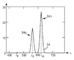
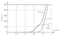
이러한 소프트웨어가 도 3a 및 도 3b에 도시된 스펙트럼 S1 및 S2의 선형 조합으로 이루어진 디바이스 광 출력의 연색 지수를 계산하는 데 사용될 때, 결과는 (스펙트럼 S1과 S2의 상이한 비율에 대응하는) 2227℃(2500K)부터 4727℃(5000K)까지의 색 온도 범위에 걸쳐 적어도 80의 연색 지수이다. 도 3a/도 3b 실시 형태에 대한 이 연색 지수가 도 5에 곡선(510)으로 나타내어져 있으며, 여기서 계산된 연색 지수(CRI)는 전체 디바이스 출력의 색 온도에 대해 표시되어 있다. 이와 유사하게, 동일한 소프트웨어가 도 4a 및 도 4b에 도시된 스펙트럼 S3 및 S4의 선형 조합으로 이루어진 디바이스 광 출력의 연색 지수를 계산하는 데 사용될 때, 결과는 (스펙트럼 S3과 S4의 상이한 비율에 대응하는) 2227℃(2500K)부터 4727℃(5000K)까지의 색 온도 범위에 걸쳐 적어도 80의 연색 지수이다. 도 4a/도 4b 실시 형태에 대한 이 연색 지수가 도 5에 곡선(512)으로 나타내어져 있다. 부가의 곡선(514)이 도 5에 제공되어 있다. 이 곡선(514)은, 제2 발광 요소(예컨대, 도 3의 지점 P2 및 도 3b의 스펙트럼 S2에 의해 특징지워지는 광 출력을 갖는 청색-LED-펌핑된 RSC)가 호박색 방출 LED를 갖지만 RSC 또는 기타 광 변환 요소를 갖지 않는 발광 요소로 대체된 것을 제외하고는, 도 3/도 3a/도 3b의 것과 유사한 실시 형태에 대하여 계산된 CRI이고, 호박색 방출 LED는 CIE 색도 다이어그램 상에서의 그의 색상이 실질적으로 또다시 도 3의 지점 P2에 대응하도록 592 ㎚의 피크 파장을 가지는 단일 스펙트럼 피크에서 광을 방출한다. 곡선(514)과 곡선(510)을 비교함으로써, CIE 색도 다이어그램 상에 표시된 바와 같이 실질적으로 동일한 색상 특성을 가지는 2개의 디바이스가 아주 상이한 연색 특성을 가질 수 있다는 것을 알 수 있다.When such software is used to calculate the color rendering index of the device light output consisting of the linear combination of spectra S1 and S2 shown in FIGS. 3A and 3B, the result is 2227 ° C. A color rendering index of at least 80 over a color temperature range from 2500K) to 4727 ° C (5000K). This color rendering index for the FIG. 3A / 3B embodiment is shown by the
예시적인 실시 형태에서, 개시된 디바이스의 연색 지수는, 예를 들어, 2227℃(2500K)부터 4727℃(5000K)까지, 또는 2727℃(3000K)부터 4727℃(5000K)까지의 색 온도 범위에 걸쳐 적어도 60, 또는 적어도 70, 또는 적어도 80이다. 높은 연색 지수 값을 달성하기 위해, 디바이스 광 출력을 이루고 있는 성분 스펙트럼(S1, S2) 각각이 적어도 2개의 개별 스펙트럼 피크(예컨대, 도 3a의 피크 S1a, S1b, 또는 도 3b의 피크 S2a, S2b) - 이들 피크가, 예를 들어, 적어도 10 ㎚만큼 서로 떨어져 있을 수 있음 - 에 의해 특징지워지도록 하는 것이 바람직하다. 게다가, 디바이스 광 출력을 이루고 있는 성분 스펙트럼 각각이, 예를 들어, 정확히 2개의 개별 스펙트럼 피크에 의해, 또는 정확히 3개의 개별 스펙트럼 피크에 의해 특징지워지도록 하는 것이 바람직할 수 있다.In an exemplary embodiment, the color rendering index of the disclosed device is, for example, at least over a color temperature range from 2227 ° C. (2500K) to 4727 ° C. (5000K), or from 2727 ° C. (3000K) to 4727 ° C. (5000K). 60, or at least 70, or at least 80. In order to achieve high color rendering index values, each of the component spectra S1, S2 constituting the device light output has at least two individual spectral peaks (e.g., peaks S1a, S1b of FIG. 3A, or peaks S2a, S2b of FIG. 3B). It is preferred that these peaks be characterized by being able to be separated from one another, for example by at least 10 nm. In addition, it may be desirable for each of the component spectra making up the device light output to be characterized by, for example, exactly two individual spectral peaks, or by exactly three individual spectral peaks.
예시적인 디바이스의 바람직한 색상-관련 특성에 대해 기술하였으며, 이제부터 이들 디바이스의 다양한 구성요소가 어떻게 물리적으로 배열될 수 있는지를, 비제한적인 방식으로, 나타내고 있는 몇몇 도면을 살펴볼 것이다.Having described the preferred color-related characteristics of the exemplary devices, we will now look at some of the drawings that illustrate, in a non-limiting manner, how the various components of these devices may be physically arranged.
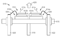
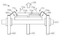
도 6은 예시적인 조명 디바이스(610)의 개략 측면도이다. 이 디바이스는 제1 발광 요소(612) 및 제2 발광 요소(614) - 둘다 금속 헤더(metal header)(616) 상에 탑재되어 있음 - 를 포함한다. 헤더(616)는 헤더와 일체로 되어 있는 제1 전도성 기둥(618)과, 서로 전기적으로 절연되어 있고 요소(612, 614)가 탑재되어 있는 디스크-형상의 헤더 메인 부분으로부터 전기적으로 절연되어 있는 제2 및 제3 전도성 기둥(620, 622)을 가진다. 기둥(620)은 와이어(624) 및 와이어 본드를 통해 제1 발광 요소(612)의 제1 전기 접점에 전기적으로 결합되고, 이와 유사하게 기둥(622)은 와이어(626) 및 와이어 본드를 통해 제2 발광 요소(614)의 제1 전기 접점에 전기적으로 결합되어 있다. 제1 및 제2 발광 요소 각각은 또한 제2 전기 접점을 가지고, 이들 전기 접점 둘다는 디스크-형상의 헤더(616) 메인 부분과 오옴 접촉하고 있고, 따라서 기둥(618)과도 오옴 접촉하고 있다.6 is a schematic side view of an
제1 발광 요소(612)는 제1 펌프 광을 방출하는 제1 전계발광 광원(612a), 및 제1 펌프 광의 적어도 일부를 제1 재방출된 광 성분으로 변환하는 제1 광 변환 요소(612b)를 포함한다. 광원(612a)은 적당한 세기 및 스펙트럼의 펌프 광을 방출하도록 구성되어 있는 LED, 레이저 다이오드 또는 유사한 고체 전계발광 광원일 수 있거나 이를 포함할 수 있다. 전술한 제1 발광 요소(612)의 제1 및 제2 전기 접점은 광원(612a) 상에 제공되고, 따라서 광원이 기둥(618, 620)에 인가되는 제1 전기 신호에 응답하여 펌프 광을 방출할 수 있다. 광 변환 요소(612b)는, 예를 들어, 하나 이상의 RSC 및/또는 하나 이상의 인광체일 수 있거나, 이를 포함할 수 있다. 요소(612)가 제1 스펙트럼 분포를 가지는 광(612c)을 방출하도록 광원(612a) 및 요소(612b)가 함께 동작한다. 광(612c)은 전형적으로 요소(612b)로부터의 적어도 제1 재방출된 광 성분을 포함하고, 또한 이상에서 상세히 기술한 바와 같은 광(612c)의 원하는 스펙트럼 특성에 따라, 광원(612a)에 의해 방출되는 제1 펌프 광의 일부를 포함할 수 있다.The first
제2 발광 요소(614)는 제2 펌프 광을 방출하는 제2 전계발광 광원(614a), 및 제2 펌프 광의 적어도 일부를 제2 재방출된 광 성분으로 변환하는 제2 광 변환 요소(614b)를 포함한다. 광원(614a)은 적당한 세기 및 스펙트럼의 펌프 광을 방출하도록 구성되어 있는 LED, 레이저 다이오드 또는 유사한 고체 전계발광 광원일 수 있거나 이를 포함할 수 있다. 전술한 제2 발광 요소(614)의 제1 및 제2 전기 접점은 광원(614a) 상에 제공되고, 따라서 광원이 기둥(618, 622)에 인가되는 제2 전기 신호에 응답하여 펌프 광을 방출할 수 있다. 광 변환 요소(614b)는, 예를 들어, 하나 이상의 RSC 및/또는 하나 이상의 인광체일 수 있거나, 이를 포함할 수 있다. 바람직하게는, 광 변환 요소(612b) 및 광 변환 요소(614b) 중 적어도 하나가 적어도 하나의 전위 우물을 포함한다. 요소(614)가 제2 스펙트럼 분포를 가지는 광(614c)을 방출하도록 광원(614a) 및 요소(614b)가 함께 동작한다. 광(614c)은 전형적으로 요소(614b)로부터의 적어도 제2 재방출된 광 성분을 포함하고, 또한 이상에서 상세히 기술한 바와 같은 광(614c)의 원하는 스펙트럼 특성에 따라, 광원(614a)에 의해 방출되는 펌프 광의 일부를 포함할 수 있다.The second
자유 공간 전파에 의해서든 광 확산기, 렌즈, 거울 등과 같은 메커니즘을 통해서든 그리고 선택적으로 기타 광 구성요소에 의해, 광(612c)과 광(614c)이 결합되어, 화살표(628)로 개략적으로 나타낸 디바이스(610)의 디바이스 광 출력을 생성한다. 디바이스 광 출력(628)은 따라서 얼마간의 광(612c)과 얼마간의 광(614c)을 포함한다. 출력(628)에 존재하는 광(612c, 614c)의 상대적인 양이 디바이스 출력(628)의 인지된 색상(예컨대, 색 온도)을 제어한다. 이들 상대적인 양, 따라서 디바이스 출력 색상이 상이한 발광 요소(612, 614)의 독립적인 또는 개별적인 전기 제어에 의해 제어될 수 있다. 따라서, 제1 발광 요소(612)는 기둥(618, 620)에 제1 전기 신호(예컨대, 주어진 크기의 전류)를 인가하는 것에 의해 전원을 공급받을 수 있다. 제2 발광 요소(614)는 기둥(618, 622)에 제1 전기 신호와 독립적인 및/또는 상이한 제2 전기 신호를 인가하는 것에 의해 전원을 공급받을 수 있다. 제1 및 제2 전기 신호의 크기는 제1 및 제2 발광 요소(612, 614)에 의해 방출되는 광의 양 및 출력(628)의 색 온도를 제어하는 데 사용된다.Light 612c and light 614c are combined, by means of free space propagation or through mechanisms such as light diffusers, lenses, mirrors, and optionally other light components, schematically represented by
도 7은 디바이스(610)와 유사한 예시적인 조명 디바이스(710)의 개략 측면도이다. 유사한 참조 번호는 유사한 요소를 나타내며, 그에 대한 추가적인 설명은 필요하지 않다. 디바이스(710)는 제1 발광 요소(712) 및 제2 발광 요소(714) - 둘다 금속 헤더(616) 상에 탑재되어 있음 - 를 포함한다. 기둥(620)은 제1 발광 요소(712)의 제1 전기 접점에 전기적으로 결합되고, 기둥(622)은 제2 발광 요소(714)의 제1 전기 접점에 전기적으로 결합되어 있다. 제1 및 제2 발광 요소 각각은 또한 제2 전기 접점을 가지고, 이들 전기 접점 둘다는 디스크-형상의 헤더(616) 메인 부분과 오옴 접촉하고 있고, 따라서 기둥(618)과도 오옴 접촉하고 있다.7 is a schematic side view of an
제1 및 제2 발광 요소(712, 714)는 전술한 요소(612, 614)와 유사하고, 제1 요소(712)는 제1 펌프 광을 방출하는 제1 전계발광 광원(712a), 및 제1 펌프 광의 적어도 일부를 제1 재방출된 광 성분으로 변환하는 제1 광 변환 요소(712b)를 포함하며, 제2 요소(714)는 제2 펌프 광을 방출하는 제2 전계발광 광원(714a), 및 제2 펌프 광의 적어도 일부를 제2 재방출된 광 성분으로 변환하는 제2 광 변환 요소(714b)를 포함한다. 광원(612a, 614a)이 개별적인 반도체(예컨대, LED) 칩에 의해 제공되는 반면 광원(712a, 714a)이 동일한 반도체(예컨대, LED) 칩 상의 개별적인 pn 접합부에 의해 제공되는 한, 전계발광 광원(712a, 714a)이 광원(612a, 614a)과 다르다. 그렇지만, 양 경우에, 제1 및 제2 전계발광 광원(612a 및 614a이든 712a 및 714a이든 상관없음)이 개별적인 전기 신호에 의해 독립적으로 및/또는 개별적으로 제어가능하다. 또한, 양 경우에, 제1 및 제2 전계발광 광원은 동일한 스펙트럼을 가지는 펌프 광을 방출할 수 있거나, 상이한 스펙트럼의 펌프 광을 방출할 수 있다.The first and second
전술한 제1 발광 요소(712)의 제1 및 제2 전기 접점은 광원(712a) 상에 제공되고, 따라서 광원이 기둥(618, 620)에 인가되는 제1 전기 신호에 응답하여 제1 펌프 광을 방출할 수 있다. 광 변환 요소(712b)는, 예를 들어, 하나 이상의 RSC 및/또는 하나 이상의 인광체일 수 있거나, 이를 포함할 수 있다. 요소(712)가 제1 스펙트럼 분포를 가지는 광(712c)을 방출하도록 광원(712a) 및 요소(712b)가 함께 동작한다. 제2 발광 요소(714)의 제1 및 제2 전기 접점은 광원(714a) 상에 제공되고, 따라서 광원이 기둥(618, 622)에 인가되는 제2 전기 신호에 응답하여 제2 펌프 광을 방출할 수 있다. 광 변환 요소(714b)가, 예를 들어, 하나 이상의 RSC 및/또는 하나 이상의 인광체일 수 있거나 이를 포함할 수 있지만, 바람직하게는 광 변환 요소(712b) 및 광 변환 요소(714b) 중 적어도 하나가 적어도 하나의 전위 우물을 포함한다. 요소(714)가 제2 스펙트럼 분포를 가지는 광(714c)을 방출하도록 광원(714a) 및 요소(714b)가 함께 동작한다. 광(714c)은 전형적으로 요소(714b)로부터의 적어도 제2 재방출된 광 성분을 포함하고, 또한 이상에서 상세히 기술한 바와 같은 광(714c)의 원하는 스펙트럼 특성에 따라, 광원(714a)에 의해 방출되는 펌프 광의 일부를 포함할 수 있다.The first and second electrical contacts of the first
주목할 점은, 도 6의 장치와 달리, 도 7에서는, 전계발광 광원(712a) 및 전계발광 광원(714a) 둘다를 덮고 있는 단일 광 변환층이 제공되고, 이러한 단일 광 변환층의 일부분이 제1 광 변환 요소(712b)를 형성하고, 이러한 단일 광 변환층의 다른 부분이 제2 광 변환 요소(714b)의 일부분을 형성한다는 것이다. 도 7에서 알 수 있는 바와 같이, 제2 광 변환 요소(714b)는 그에 부가하여 제1 광 변환 요소(712b)에 존재하지 않는 또 하나의 광 변환 요소를 포함한다.It should be noted that, unlike the apparatus of FIG. 6, in FIG. 7, a single light conversion layer is provided covering both the electroluminescent
자유 공간 전파에 의해서든 광 확산기, 렌즈, 거울 등과 같은 메커니즘을 통해서든 그리고 선택적으로 기타 광 구성요소에 의해, 광(712c)과 광(714c)이 결합되어, 화살표(728)로 개략적으로 나타낸 디바이스(710)의 디바이스 광 출력을 생성한다. 출력(728)에 존재하는 광(712c, 714c)의 상대적인 양이 디바이스 출력(728)의 색 온도 또는 기타 인지된 색상을 제어한다. 이들 상대적인 양, 따라서 디바이스 출력 색상이 상이한 발광 요소(712, 714)의 독립적인 또는 개별적인 전기 제어에 의해 제어될 수 있다. 따라서, 제1 발광 요소(712)는 기둥(618, 620)에 제1 전기 신호를 인가하는 것에 의해 전원을 공급받을 수 있고, 제2 발광 요소(714)는 기둥(618, 622)에 제1 전기 신호와 독립적인 및/또는 상이한 제2 전기 신호를 인가하는 것에 의해 전원을 공급받을 수 있다. 제1 및 제2 전기 신호의 크기는 제1 및 제2 발광 요소(712, 714)에 의해 방출되는 광의 양 및 출력(728)의 색 온도를 제어하는 데 사용된다.Light 712c and light 714c are combined, by means of free space propagation or through mechanisms such as light diffusers, lenses, mirrors, and optionally other light components, schematically represented by
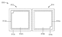
도 8은 다른 조명 디바이스(810)의 개략 평면도로서, 이 디바이스(810)의 설계가 실질적으로 디바이스(610, 도 6) 또는 디바이스(710, 도 7) 중 어느 하나에 적용될 수 있다. 디바이스(810)는 제1 발광 요소(812) 및 제2 발광 요소(814)를 포함한다. 좁은 선폭을 갖는 일반적으로 정사각형-형상의 전기 접점(812a)이 제1 요소(812)의 제1 전계발광 광원 상에 제공된다. 요소(812)는 또한 정사각형-형상의 접점(812a)으로 둘러싸인 요소(812)의 적어도 중앙 영역에 배치된 제1 광 변환 요소(812b)를 포함한다. 요소(812)의 주변 영역(812c)은 또한 제1 광 변환 요소(812b)로 덮여 있을 수 있거나, 광 변환 요소를 포함하지 않고 오히려 단순히 제1 전계발광 광원의 노출된 부분일 수 있다.8 is a schematic plan view of another
좁은 선폭을 갖는 일반적으로 정사각형-형상의 다른 전기 접점(814a)이 또한 제2 요소(814)의 제2 전계발광 광원 상에 제공된다. 요소(814)는 또한 정사각형-형상의 접점(814a)으로 둘러싸인 요소(814)의 적어도 중앙 영역에 배치된 제2 광 변환 요소(814b)를 포함한다. 요소(812)의 주변 영역(814c)은 또한 제2 광 변환 요소(812b)로 덮여 있을 수 있거나, 광 변환 요소를 포함하지 않고 오히려 단순히 제2 전계발광 광원의 노출된 부분일 수 있다.Another generally square-shaped
도 9는 다른 조명 디바이스(910)의 개략 평면도로서, 이 디바이스(910)의 설계가 실질적으로, 예를 들어, 디바이스(710, 도 7)에 적용될 수 있다. 디바이스(910)는 일반적으로 U자-형상의 제1 발광 요소(912) 및 일반적으로 U자-형상의 제2 발광 요소(914)를 포함하고, 이 2개의 요소는 인터로킹 패턴(interlocking pattern)을 형성하여 일반적으로 정사각형의 전체 윤곽선 또는 경계를 제공한다. 좁은 선폭을 갖는 일반적으로 U자-형상의 전기 접점(912a)이 제1 요소(912)의 제1 전계발광 광원 상에 제공된다. 요소(912)는 또한 접점(912a)에 가까운 영역에서 제1 전계발광 광원 상에 배치된 제1 광 변환 요소(912b)를 포함한다.9 is a schematic plan view of another
좁은 선폭을 갖는 일반적으로 U자-형상의 다른 전기 접점(914a)이 또한 제2 요소(914)의 제2 전계발광 광원 상에 제공된다. 요소(914)는 또한 접점(914a)에 가까운 영역에서 제2 전계발광 광원 상에 배치된 제2 광 변환 요소(914b)를 포함한다.Another generally U-shaped
디바이스(910)의 나머지 영역(914c)은 제1 광 변환 요소(912b) 및/또는 제2 광 변환 요소(914b)로 덮여 있을 수 있거나, 광 변환 요소를 포함하지 않고 오히려 단순히 제1 및/또는 제2 전계발광 광원의 노출된 부분일 수 있다. 디바이스(910)의 인터디지트된(interdigited) 설계는 전계발광 요소(912, 914)로부터의 광을 혼합하는 것을 용이하게 해줄 수 있다.The remaining
도 6 및 도 7의 실시 형태는 조명 디바이스의 2개의 발광 요소가 3개의 전기 단자 또는 접점을 사용하여 어떻게 독립적으로 제어될 수 있는지를 설명하며, 여기서 하나의 단자[기둥(618)]가 양 요소에 공통이고, 다른 단자들[기둥(620, 622)] 각각은 요소들 중 하나에만 전용되어 있다. 한 쌍의 단자[기둥(618, 620)]에 제1 전기 신호를 인가하고 다른 쌍의 단자[기둥(618, 622)]에 (제1 전기 신호와 독립적인) 제2 전기 신호를 인가하는 것에 의해 독립적인 제어가 달성될 수 있다. 물론, 4 단자 디바이스도 생각되며, 이 경우 어떤 단자도 양 요소에 공통이 아니며, 주어진 쌍의 단자가 발광 요소들 중 주어진 발광 요소에 전용되어 있다.6 and 7 illustrate how two light emitting elements of a lighting device can be independently controlled using three electrical terminals or contacts, where one terminal [column 618] is an element of both. Common to each other, each of the other terminals (
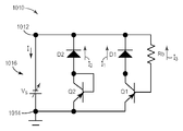
도 10에서, 단지 2개의 입력 단자를 가지며 2개의 입력 단자에 제공되는 전기 입력의 크기의 함수로서 색상 제어 또는 조정을 달성하기 위해 개시된 조명 디바이스의 2개의 발광 요소를 상이한 양으로 구동하는 데 사용될 수 있는 회로(1010)를 개시하고 있다. 이 회로에서, 단자(1012, 1014)는 입력 단자이다. 외부의 가변 또는 조정가능 광원(1016)이, 도시된 바와 같이, 입력 단자에 결합되어 있다. 전원(1016) - 전압원 또는 전류원일 수 있음 - 은 가변 전압 Vs 및 가변 전류 I를 조명 디바이스에 제공한다. 조명 디바이스는 제1 전계발광 광원 및 제1 전계발광 광원에 의해 제공된 펌프광의 적어도 일부를 제1 재방출된 광 성분으로 변환하는 제1 광 변환 요소를 가지는 제1 발광 요소를 포함한다. 조명 디바이스는 또한 제2 전계발광 광원 및 제2 전계발광 광원에 의해 제공된 펌프광의 적어도 일부를 제2 재방출된 광 성분으로 변환하는 제2 광 변환 요소를 가지는 제2 발광 요소를 포함한다.In FIG. 10, two light emitting elements of the disclosed lighting device can be used to drive different amounts of light to achieve color control or adjustment as a function of the magnitude of the electrical input provided to the two input terminals. A
회로(1010)에서, 예를 들어, LED일 수 있거나 이를 포함할 수 있는 제1 전계발광 광원이 다이오드 D1으로 표현되어 있고, 상이한 LED일 수 있거나 이를 포함할 수 있는 제2 전계발광 광원이 다이오드 D2로 표현되어 있다. 회로(1010)를 완성하기 위해, 이 다이오드가, 도시된 바와 같이, 다른 회로 요소(즉, 트랜지스터 Q1 및 Q2와 베이스 저항기 Rb)에 연결되어 있다. 다이오드 D1, 다이오드 D2, 및 베이스 저항기 Rb를 통해 흐르는 전류는, 각각, I1, I2, 및 I3로 표시되어 있다. 이들 전류가 합해져 소스 전류 I가 된다(즉, I1 + I2 + I3 = I). 주목할 점은, 트랜지스터 Q1 및 베이스 저항기 Rb가 연결되어 있는 것으로 인해 다이오드 D1을 통해 흐르는 전류 I1이 주로 Rb 및 트랜지스터 Q1의 전류 이득에 의해 결정되는 값으로 실질적으로 제한된다는 것이다. 한편, 트랜지스터 Q2가 다이오드로서 기능하도록 결선되어 있는 것으로 인해 다이오드 D1을 포함하는 회로의 분기가 포화되고 나서 상당한 후까지 다이오드 D2가 턴온(turn on)되지 않는다.In
입력 단자(1012, 1014)에 인가된 전기 신호에 응답한 이들 차이로 인해 상이한 상대적 양의 광이 다이오드 D1 및 D2에 의해 방출되고, 따라서 상이한 상대적 양의 광이 조명 디바이스의 제1 및 제2 발광 요소에 의해 방출되며, 따라서 인가된 전기 신호의 크기의 함수로서, 상이한 색상 또는 색 온도가 조명 디바이스 광 출력에 의해 제공된다. 예를 들어, 제1 발광 요소(다이오드 D1이 그의 일부임)가 따뜻한 백색 광을 방출하고 제2 발광 요소(다이오드 D2가 그의 일부임)가 시원한 백색 광을 방출하는 경우, 회로(1010)의 효과는 낮은 인가된 전류에서 실질적으로 따뜻한 백색 광의 결합된 출력(즉, 조명 디바이스 광 출력)을 제공하지만 인가된 전류가 증가됨에 따라 이 출력이 점진적으로 보다 시원하고 밝은 백색으로 천이한다는 것이다. 이러한 성능이 바람직할 수 있는데, 그 이유는 백열 광원의 익숙한 조광 거동과 비슷하기 때문이다. 회로(1010)는 따라서 색상-변경 조광 회로로서 동작할 수 있다.Due to these differences in response to the electrical signals applied to the
완전함을 위해, 도 11a 및 도 11b는 회로(1010)의 모델링된 거동을 나타낸 것으로서, 여기서 Rb의 값은 500 오옴으로 가정되었다. 양 도면에서, y축은 주어진 회로 요소 또는 요소들을 통해 흐르는 전류(단위: 밀리암페어)를 나타낸다. 도 11a에서, x축은 외부 전원에 의해 제공되는 전압 Vs를 나타낸다. 곡선(1110)은 다이오드 D1을 통해 흐르는 전류 I1을 나타내고, 곡선(1112)은 다이오드 D2를 통해 흐르는 전류 I2를 나타내며, 곡선(1114)은 이들 전류의 합 I1 + I2를 나타낸다. 도 11b에서, x축은 양 다이오드를 통해 흐르는 총 전류(즉, I1 + I2)를 나타낸다. 곡선(1116)은 다이오드 D1을 통해 흐르는 전류 I1을 나타내고, 곡선(1118)은 다이오드 D2를 통해 흐르는 전류 I2를 나타낸다.For the sake of completeness, FIGS. 11A and 11B show the modeled behavior of
회로(1010)의 하나 이상의 구성요소(트랜지스터 및/또는 베이스 저항기 등)는 "금속 본드형(metal bonded)" GaN LED에 사용되는 규소 기판 또는 기타 반도체 기판에 제조될 수 있다. 대안적으로, 이러한 회로 구성요소는 광 방출을 맡고 있는 반도체 디바이스로부터 멀리 떨어져 물리적으로 분리되도록 제조될 수 있다.One or more components of the circuit 1010 (such as transistors and / or base resistors) may be fabricated on silicon substrates or other semiconductor substrates used in " metal bonded " GaN LEDs. Alternatively, such circuit components can be manufactured to be physically separated away from the semiconductor device that is responsible for emitting light.
달리 언급하지 않는 한, 본 명세서 및 특허청구범위에 사용되는 양, 특성의 측정치 등을 표현하는 모든 숫자는 "약"이라는 용어에 의해 수식되는 것으로 이해되어야 한다. 그에 따라, 달리 언급하지 않는 한, 명세서 및 특허청구범위에 기술되는 숫자 파라미터는 본 출원의 개시 내용을 이용하여 당업자가 달성하고자 하는 원하는 특성에 따라 다를 수 있는 근사치이다. 특허청구범위의 범주에 대한 등가물의 원칙의 적용을 제한하려고 시도함이 없이, 각각의 수치적 파라미터는 적어도 보고된 유효 숫자의 수의 관점에서 그리고 통상의 반올림 기법을 적용하여 해석되어야 한다. 본 발명의 넓은 범주를 기술하는 수치 범위 및 파라미터가 근사치임에도 불구하고, 임의의 수치 값이 본 명세서에 설명된 특정 예에 기술되는 한, 이들은 가능한 한 합리적으로 정확히 보고된다. 그러나, 임의의 수치 값은 시험 또는 측정 한계와 관련된 오차를 분명히 포함할 수 있다.Unless stated otherwise, all numbers expressing quantities, measurements of properties, and the like, used in this specification and claims are to be understood as being modified by the term "about." Accordingly, unless indicated to the contrary, the numerical parameters set forth in the specification and claims are approximations that may vary depending upon the desired properties sought by those skilled in the art using the disclosure of this application. Without attempting to limit the application of the principles of equivalents to the scope of the claims, each numerical parameter should be interpreted at least in terms of the number of reported significant digits and by applying the usual rounding techniques. Notwithstanding that the numerical ranges and parameters setting forth the broad scope of the invention are approximations, as far as any numerical value is set forth in the specific examples described herein, they are reported as reasonably accurate as possible. However, any numerical value may clearly include an error associated with a test or measurement limit.
본 발명의 다양한 수정 및 변경이 본 발명의 사상 및 범위를 벗어나지 않고 기술 분야의 당업자에게는 명백할 것이며, 본 발명이 본 명세서에 기술된 예시적인 실시 형태로 제한되지 않는다는 것을 잘 알 것이다. 예를 들어, 읽는 사람은, 달리 언급하지 않는 한, 하나의 개시된 실시 형태의 특징이 또한 모든 다른 개시된 실시 형태에도 적용될 수 있는 것으로 가정해야 한다. 또한, 본 명세서에서 언급된 모든 미국 특허, 특허 출원 공개, 및 기타 특허와 비특허 문서가, 이상의 개시 내용과 모순되지 않는 한, 참조 문헌으로서 포함된다는 것을 잘 알 것이다.Various modifications and variations of the present invention will be apparent to those skilled in the art without departing from the spirit and scope of the invention, and it will be appreciated that the invention is not limited to the exemplary embodiments described herein. For example, the reader should assume that features of one disclosed embodiment can also be applied to all other disclosed embodiments unless otherwise noted. It is also to be understood that all US patents, patent application publications, and other patents and non-patent documents mentioned herein are incorporated by reference, unless they contradict the above disclosure.
Claims (23)
제1 스펙트럼 분포를 가지는 광을 방출하도록 구성된 제1 발광 요소(luminescent element) - 제1 발광 요소는 제1 펌프 광(pump light)을 방출하는 제1 전계발광 광원(electroluminescent source), 및 제1 펌프 광의 적어도 일부를 제1 재방출된 광 성분으로 변환하는 제1 광 변환 요소(light converting element)를 포함함 -, 및
제2 스펙트럼 분포를 가지는 광을 방출하도록 구성된 제2 발광 요소 - 제2 발광 요소는 제2 펌프 광을 방출하는 제2 전계발광 광원, 및 제2 펌프 광의 적어도 일부를 제2 재방출된 광 성분으로 변환하는 제2 광 변환 요소를 포함함 - 를 포함하고,
제1 및 제2 광 변환 요소 중 적어도 하나는 제1 전위 우물을 포함하는 제1 반도체 적층물을 포함하며,
제1 및 제2 발광 요소는 제1 및 제2 발광 요소에 의해 방출된 광이 결합되어 디바이스 출력을 제공하도록 배치되어 있고,
제1 및 제2 스펙트럼 분포는, 각각, 표준 CIE (x,y) 색 좌표 다이어그램에서 라인 세그먼트 상의 제1 및 제2 종점에 의해 표현될 수 있고, 라인 세그먼트는 제1 발광 요소에 의해 방출된 광 및 제2 발광 요소에 의해 방출된 광의 상이한 상대적 양에 대한 가능한 디바이스 출력의 범위를 나타내며, 라인 세그먼트의 적어도 일부분은 또한 적어도 2727℃(3000K)부터 4727℃(5000K)까지의 색 온도 범위에 걸쳐 플랑키안 궤적(Planckian locus)에 가까운 것인 디바이스.As a solid state lighting device,
A first luminescent element configured to emit light having a first spectral distribution, the first luminescent element comprising a first electroluminescent source that emits a first pump light, and a first pump A first light converting element for converting at least a portion of the light into a first re-emitted light component; and
A second light emitting element configured to emit light having a second spectral distribution, the second light emitting element being a second electroluminescent light source for emitting a second pump light, and at least a portion of the second pump light as a second re-emitted light component Includes a second light converting element to convert;
At least one of the first and second light conversion elements comprises a first semiconductor stack comprising a first potential well,
The first and second light emitting elements are arranged such that the light emitted by the first and second light emitting elements is combined to provide device output,
The first and second spectral distributions may be represented by first and second endpoints on the line segment in the standard CIE (x, y) color coordinate diagram, respectively, wherein the line segment is light emitted by the first light emitting element. And a range of possible device outputs for different relative amounts of light emitted by the second light emitting element, wherein at least a portion of the line segment is also planed over a color temperature range from at least 2727 ° C. (3000K) to 4727 ° C. (5000K). A device close to the Planckian locus.
Applications Claiming Priority (2)
| Application Number | Priority Date | Filing Date | Title |
|---|---|---|---|
| US22166009P | 2009-06-30 | 2009-06-30 | |
| US61/221,660 | 2009-06-30 |
Publications (1)
| Publication Number | Publication Date |
|---|---|
| KR20120092549A true KR20120092549A (en) | 2012-08-21 |
Family
ID=42646301
Family Applications (1)
| Application Number | Title | Priority Date | Filing Date |
|---|---|---|---|
| KR1020127002033A KR20120092549A (en) | 2009-06-30 | 2010-06-25 | White light electroluminescent devices with adjustable color temperature |
Country Status (7)
| Country | Link |
|---|---|
| US (1) | US8629611B2 (en) |
| EP (1) | EP2449856A1 (en) |
| JP (2) | JP2012532453A (en) |
| KR (1) | KR20120092549A (en) |
| CN (1) | CN102474932B (en) |
| TW (1) | TW201130107A (en) |
| WO (1) | WO2011002686A1 (en) |
Families Citing this family (22)
| Publication number | Priority date | Publication date | Assignee | Title |
|---|---|---|---|---|
| KR20120015337A (en) | 2009-05-05 | 2012-02-21 | 쓰리엠 이노베이티브 프로퍼티즈 컴파니 | Re-emitting semiconductor carrier devices for use with leds and methods of manufacture |
| JP2012526392A (en) | 2009-05-05 | 2012-10-25 | スリーエム イノベイティブ プロパティズ カンパニー | Re-emitting semiconductor structure with improved extraction efficiency |
| EP2427921A1 (en) | 2009-05-05 | 2012-03-14 | 3M Innovative Properties Company | Semiconductor devices grown on indium-containing substrates utilizing indium depletion mechanisms |
| CN102473816B (en) | 2009-06-30 | 2015-03-11 | 3M创新有限公司 | Electroluminescent devices with color adjustment based on current crowding |
| KR20120094463A (en) | 2009-06-30 | 2012-08-24 | 쓰리엠 이노베이티브 프로퍼티즈 컴파니 | Cadmium-free re-emitting semiconductor construction |
| JP2014503117A (en) | 2010-12-29 | 2014-02-06 | スリーエム イノベイティブ プロパティズ カンパニー | Remote phosphor LED device with broadband output and controllable color |
| JP5906433B2 (en) * | 2011-12-19 | 2016-04-20 | パナソニックIpマネジメント株式会社 | Lighting device |
| DE102012105208A1 (en) * | 2012-06-15 | 2013-12-19 | Osram Opto Semiconductors Gmbh | Semiconductor light source |
| WO2014042706A1 (en) | 2012-09-13 | 2014-03-20 | 3M Innovative Properties Company | Efficient lighting system with wide color range |
| EP2953174B1 (en) * | 2013-01-31 | 2020-07-01 | Kabushiki Kaisha Toshiba | Light emitting device and led light bulb |
| WO2014140976A1 (en) * | 2013-03-11 | 2014-09-18 | Koninklijke Philips N.V. | A dimmable light emitting arrangement |
| DE102013206154A1 (en) * | 2013-04-08 | 2014-10-09 | Zumtobel Lighting Gmbh | Lighting device with variably adjustable light color |
| JP2015050270A (en) * | 2013-08-30 | 2015-03-16 | 株式会社東芝 | Semiconductor light-emitting device |
| FR3012677B1 (en) * | 2013-10-25 | 2015-12-25 | Commissariat Energie Atomique | LIGHT EMISSIVE DEVICE, DEVICE AND METHOD FOR ADJUSTING A LIGHT EMITTING OF A PHOSPHORUS LIGHT EMITTING DIODE |
| JP6014007B2 (en) * | 2013-11-08 | 2016-10-25 | 豊田合成株式会社 | Lighting device |
| US9215761B2 (en) * | 2014-05-15 | 2015-12-15 | Cree, Inc. | Solid state lighting devices with color point non-coincident with blackbody locus |
| DE102015202159B4 (en) * | 2015-02-06 | 2023-06-15 | OSRAM Opto Semiconductors Gesellschaft mit beschränkter Haftung | semiconductor lighting device |
| JP6696129B2 (en) * | 2015-08-28 | 2020-05-20 | 日亜化学工業株式会社 | Light emitting device |
| CN107420748B (en) * | 2017-07-25 | 2019-11-19 | 江苏集萃有机光电技术研究所有限公司 | The luminescent device of adjustable color temperature and colour rendering index, adjusting method and lamps and lanterns |
| CN109038207B (en) * | 2018-07-27 | 2020-11-27 | 中国科学院苏州纳米技术与纳米仿生研究所 | Temperature-controllable VCSEL device and manufacturing method thereof |
| CN109379813B (en) * | 2018-12-07 | 2021-08-17 | 深圳和而泰智能控制股份有限公司 | Color temperature adjustable illumination module and color temperature adjusting method of illumination module |
| US10887960B2 (en) * | 2019-03-28 | 2021-01-05 | Lumileds Llc | Color tunable light emitting diode (LED) systems, LED lighting systems, and methods |
Family Cites Families (65)
| Publication number | Priority date | Publication date | Assignee | Title |
|---|---|---|---|---|
| US3526801A (en) | 1964-08-07 | 1970-09-01 | Honeywell Inc | Radiation sensitive semiconductor device |
| JPH077847B2 (en) | 1984-12-17 | 1995-01-30 | 株式会社東芝 | Semiconductor light emitting element |
| US5048035A (en) | 1989-05-31 | 1991-09-10 | Kabushiki Kaisha Toshiba | Semiconductor light emitting device |
| JP2871477B2 (en) | 1994-09-22 | 1999-03-17 | 信越半導体株式会社 | Semiconductor light emitting device and method of manufacturing the same |
| JPH10500534A (en) | 1995-03-10 | 1998-01-13 | フィリップス エレクトロニクス ネムローゼ フェンノートシャップ | Illumination system for controlling color temperature of artificial light under the influence of daylight level |
| EP1010773A4 (en) | 1997-02-19 | 2004-08-25 | Kirin Brewery | Method and apparatus for producing plastic container having carbon film coating |
| US7014336B1 (en) | 1999-11-18 | 2006-03-21 | Color Kinetics Incorporated | Systems and methods for generating and modulating illumination conditions |
| US6016038A (en) | 1997-08-26 | 2000-01-18 | Color Kinetics, Inc. | Multicolored LED lighting method and apparatus |
| JP3358556B2 (en) | 1998-09-09 | 2002-12-24 | 日本電気株式会社 | Semiconductor device and manufacturing method thereof |
| AU5463700A (en) | 1999-06-04 | 2000-12-28 | Trustees Of Boston University | Photon recycling semiconductor multi-wavelength light-emitting diodes |
| FR2801814B1 (en) | 1999-12-06 | 2002-04-19 | Cebal | METHOD FOR DEPOSITING A COATING ON THE INTERNAL SURFACE OF AEROSOL DISPENSING UNITS |
| US6902987B1 (en) | 2000-02-16 | 2005-06-07 | Ziptronix, Inc. | Method for low temperature bonding and bonded structure |
| TW497277B (en) | 2000-03-10 | 2002-08-01 | Toshiba Corp | Semiconductor light emitting device and method for manufacturing the same |
| US7202613B2 (en) | 2001-05-30 | 2007-04-10 | Color Kinetics Incorporated | Controlled lighting methods and apparatus |
| US6636003B2 (en) | 2000-09-06 | 2003-10-21 | Spectrum Kinetics | Apparatus and method for adjusting the color temperature of white semiconduct or light emitters |
| IL138471A0 (en) | 2000-09-14 | 2001-10-31 | Yissum Res Dev Co | Novel semiconductor materials and their uses |
| WO2002041362A2 (en) | 2000-11-17 | 2002-05-23 | Emcore Corporation | Laser separated die with tapered sidewalls for improved light extraction |
| US7358679B2 (en) | 2002-05-09 | 2008-04-15 | Philips Solid-State Lighting Solutions, Inc. | Dimmable LED-based MR16 lighting apparatus and methods |
| CA2427559A1 (en) | 2002-05-15 | 2003-11-15 | Sumitomo Electric Industries, Ltd. | White color light emitting device |
| ATE468147T1 (en) | 2003-01-16 | 2010-06-15 | Femmepharma Holding Co Inc | VAGINAL OR RECTAL APPLICATOR AND METHOD |
| JP2005005482A (en) * | 2003-06-12 | 2005-01-06 | Citizen Electronics Co Ltd | Led light emitting device and color display device using the same |
| NO20041523L (en) | 2003-09-19 | 2005-03-21 | Sumitomo Electric Industries | Light emitting semiconductor element |
| JP2005101296A (en) * | 2003-09-25 | 2005-04-14 | Osram-Melco Ltd | Device, module, and lighting apparatus of variable color light emitting diode |
| DE10354936B4 (en) | 2003-09-30 | 2012-02-16 | Osram Opto Semiconductors Gmbh | Radiation-emitting semiconductor component |
| US7026653B2 (en) | 2004-01-27 | 2006-04-11 | Lumileds Lighting, U.S., Llc | Semiconductor light emitting devices including current spreading layers |
| TWI229465B (en) | 2004-03-02 | 2005-03-11 | Genesis Photonics Inc | Single chip white light component |
| TWI243489B (en) | 2004-04-14 | 2005-11-11 | Genesis Photonics Inc | Single chip light emitting diode with red, blue and green three wavelength light emitting spectra |
| US7361938B2 (en) | 2004-06-03 | 2008-04-22 | Philips Lumileds Lighting Company Llc | Luminescent ceramic for a light emitting device |
| US7553683B2 (en) | 2004-06-09 | 2009-06-30 | Philips Lumiled Lighting Co., Llc | Method of forming pre-fabricated wavelength converting elements for semiconductor light emitting devices |
| US7126160B2 (en) | 2004-06-18 | 2006-10-24 | 3M Innovative Properties Company | II-VI/III-V layered construction on InP substrate |
| US7119377B2 (en) | 2004-06-18 | 2006-10-10 | 3M Innovative Properties Company | II-VI/III-V layered construction on InP substrate |
| US7534633B2 (en) | 2004-07-02 | 2009-05-19 | Cree, Inc. | LED with substrate modifications for enhanced light extraction and method of making same |
| US7223998B2 (en) | 2004-09-10 | 2007-05-29 | The Regents Of The University Of California | White, single or multi-color light emitting diodes by recycling guided modes |
| JP2008516456A (en) | 2004-10-08 | 2008-05-15 | ザ リージェンツ オブ ザ ユニヴァーシティー オブ カリフォルニア | High efficiency light emitting diode |
| US7402831B2 (en) * | 2004-12-09 | 2008-07-22 | 3M Innovative Properties Company | Adapting short-wavelength LED's for polychromatic, broadband, or “white” emission |
| US7804100B2 (en) | 2005-03-14 | 2010-09-28 | Philips Lumileds Lighting Company, Llc | Polarization-reversed III-nitride light emitting device |
| US7417260B2 (en) | 2005-06-28 | 2008-08-26 | Dong-Sing Wuu | Multiple-chromatic light emitting device |
| US20080272712A1 (en) | 2005-09-19 | 2008-11-06 | Koninklijke Philips Electronics, N.V. | Variable Color Light Emitting Device and Method for Controlling the Same |
| US7285791B2 (en) | 2006-03-24 | 2007-10-23 | Goldeneye, Inc. | Wavelength conversion chip for use in solid-state lighting and method for making same |
| KR100875443B1 (en) | 2006-03-31 | 2008-12-23 | 서울반도체 주식회사 | Light emitting device |
| US20070284565A1 (en) | 2006-06-12 | 2007-12-13 | 3M Innovative Properties Company | Led device with re-emitting semiconductor construction and optical element |
| US7902542B2 (en) | 2006-06-14 | 2011-03-08 | 3M Innovative Properties Company | Adapted LED device with re-emitting semiconductor construction |
| JP4989936B2 (en) * | 2006-07-27 | 2012-08-01 | 株式会社朝日ラバー | Lighting device |
| KR100829925B1 (en) | 2007-03-02 | 2008-05-16 | 세메스 주식회사 | Apparatus and method for processing substrate |
| CN101627482A (en) | 2007-03-08 | 2010-01-13 | 3M创新有限公司 | Array of luminescent elements |
| US7288902B1 (en) | 2007-03-12 | 2007-10-30 | Cirrus Logic, Inc. | Color variations in a dimmable lighting device with stable color temperature light sources |
| US7687816B2 (en) | 2007-03-20 | 2010-03-30 | International Business Machines Corporation | Light emitting diode |
| US7759854B2 (en) * | 2007-05-30 | 2010-07-20 | Global Oled Technology Llc | Lamp with adjustable color |
| US10505083B2 (en) | 2007-07-11 | 2019-12-10 | Cree, Inc. | Coating method utilizing phosphor containment structure and devices fabricated using same |
| WO2009036579A1 (en) | 2007-09-21 | 2009-03-26 | Hoffmann Neopac Ag | Apparatus for plasma supported coating of the inner surface of tube-like packaging containers made of plastics with the assistance of a non-thermal reactive ambient pressure beam plasma |
| CN101821866B (en) | 2007-10-08 | 2012-05-23 | 3M创新有限公司 | Light emitting diode with bonded semiconductor wavelength converter |
| US9012937B2 (en) * | 2007-10-10 | 2015-04-21 | Cree, Inc. | Multiple conversion material light emitting diode package and method of fabricating same |
| US20090108269A1 (en) | 2007-10-26 | 2009-04-30 | Led Lighting Fixtures, Inc. | Illumination device having one or more lumiphors, and methods of fabricating same |
| EP2301087A2 (en) | 2008-06-05 | 2011-03-30 | 3M Innovative Properties Company | Light emitting diode with bonded semiconductor wavelength converter |
| WO2009158138A2 (en) | 2008-06-26 | 2009-12-30 | 3M Innovative Properties Company | Semiconductor light converting construction |
| KR20110031953A (en) | 2008-06-26 | 2011-03-29 | 쓰리엠 이노베이티브 프로퍼티즈 컴파니 | Semiconductor light converting construction |
| WO2010019594A2 (en) | 2008-08-14 | 2010-02-18 | 3M Innovative Properties Company | Projection system with imaging light source module |
| JP2012502473A (en) | 2008-09-04 | 2012-01-26 | スリーエム イノベイティブ プロパティズ カンパニー | II-VI multiple quantum well vertical cavity surface emitting laser on a heat sink optically pumped by a gallium nitride laser diode |
| KR20110053382A (en) | 2008-09-08 | 2011-05-20 | 쓰리엠 이노베이티브 프로퍼티즈 컴파니 | Electrically pixelated luminescent device |
| US8619620B2 (en) | 2008-09-16 | 2013-12-31 | Qualcomm Incorporated | Methods and systems for transmission mode selection in a multi channel communication system |
| CN102318089A (en) | 2008-12-24 | 2012-01-11 | 3M创新有限公司 | Light generating device with two-sided wavelength shifter |
| JP2012526392A (en) | 2009-05-05 | 2012-10-25 | スリーエム イノベイティブ プロパティズ カンパニー | Re-emitting semiconductor structure with improved extraction efficiency |
| EP2427921A1 (en) | 2009-05-05 | 2012-03-14 | 3M Innovative Properties Company | Semiconductor devices grown on indium-containing substrates utilizing indium depletion mechanisms |
| CN102473816B (en) | 2009-06-30 | 2015-03-11 | 3M创新有限公司 | Electroluminescent devices with color adjustment based on current crowding |
| KR20120094463A (en) | 2009-06-30 | 2012-08-24 | 쓰리엠 이노베이티브 프로퍼티즈 컴파니 | Cadmium-free re-emitting semiconductor construction |
-
2010
- 2010-06-25 KR KR1020127002033A patent/KR20120092549A/en not_active Application Discontinuation
- 2010-06-25 EP EP10730307A patent/EP2449856A1/en not_active Withdrawn
- 2010-06-25 US US13/379,895 patent/US8629611B2/en not_active Expired - Fee Related
- 2010-06-25 JP JP2012517777A patent/JP2012532453A/en active Pending
- 2010-06-25 WO PCT/US2010/040017 patent/WO2011002686A1/en active Application Filing
- 2010-06-25 CN CN201080029543.6A patent/CN102474932B/en not_active Expired - Fee Related
- 2010-06-29 TW TW099121301A patent/TW201130107A/en unknown
-
2015
- 2015-02-09 JP JP2015023239A patent/JP6140742B2/en not_active Expired - Fee Related
Also Published As
| Publication number | Publication date |
|---|---|
| JP6140742B2 (en) | 2017-05-31 |
| US8629611B2 (en) | 2014-01-14 |
| US20120104935A1 (en) | 2012-05-03 |
| EP2449856A1 (en) | 2012-05-09 |
| CN102474932A (en) | 2012-05-23 |
| JP2012532453A (en) | 2012-12-13 |
| WO2011002686A1 (en) | 2011-01-06 |
| CN102474932B (en) | 2015-12-16 |
| TW201130107A (en) | 2011-09-01 |
| JP2015149480A (en) | 2015-08-20 |
Similar Documents
| Publication | Publication Date | Title |
|---|---|---|
| JP6140742B2 (en) | White light electroluminescent device with adjustable color temperature | |
| US11600605B2 (en) | White light emitting devices having high luminous efficiency and improved color rendering that include pass-through violet emissions | |
| US10074781B2 (en) | Semiconductor light emitting devices including multiple red phosphors that exhibit good color rendering properties with increased brightness | |
| US10541353B2 (en) | Light emitting devices including narrowband converters for outdoor lighting applications | |
| US9006986B2 (en) | Semiconductor light emitting devices having selectable and/or adjustable color points and related methods | |
| US8796952B2 (en) | Semiconductor light emitting devices having selectable and/or adjustable color points and related methods | |
| DE102008021572B4 (en) | Solid-state lamp and luminaire with it | |
| US20140167601A1 (en) | Enhanced Luminous Flux Semiconductor Light Emitting Devices Including Red Phosphors that Exhibit Good Color Rendering Properties and Related Red Phosphors | |
| US9219202B2 (en) | Semiconductor light emitting devices including red phosphors that exhibit good color rendering properties and related red phosphors | |
| US8178888B2 (en) | Semiconductor light emitting devices with high color rendering | |
| US20130015461A1 (en) | Light-emitting Device Capable of Producing White Light And Light Mixing Method For Producing White Light With Same | |
| US8304976B2 (en) | Electroluminescent devices with color adjustment based on current crowding | |
| US20160254421A1 (en) | White light emitting devices including both red and multi-phosphor blue-shifted-yellow solid state emitters | |
| WO2021067821A1 (en) | Light emitting diode package with a plurality of lumiphoric regions | |
| US9054278B2 (en) | Lighting apparatuses and driving methods regarding to light-emitting diodes |
Legal Events
| Date | Code | Title | Description |
|---|---|---|---|
| WITN | Application deemed withdrawn, e.g. because no request for examination was filed or no examination fee was paid |