JP2012529169A - 逆層配列を含む光活性コンポーネントおよび前記コンポーネントを製造する方法 - Google Patents
逆層配列を含む光活性コンポーネントおよび前記コンポーネントを製造する方法 Download PDFInfo
- Publication number
- JP2012529169A JP2012529169A JP2012513638A JP2012513638A JP2012529169A JP 2012529169 A JP2012529169 A JP 2012529169A JP 2012513638 A JP2012513638 A JP 2012513638A JP 2012513638 A JP2012513638 A JP 2012513638A JP 2012529169 A JP2012529169 A JP 2012529169A
- Authority
- JP
- Japan
- Prior art keywords
- type
- layer
- photoactive
- photoactive component
- doped
- Prior art date
- Legal status (The legal status is an assumption and is not a legal conclusion. Google has not performed a legal analysis and makes no representation as to the accuracy of the status listed.)
- Pending
Links
- 230000002441 reversible effect Effects 0.000 title claims description 5
- 238000000034 method Methods 0.000 title description 10
- 238000004519 manufacturing process Methods 0.000 title description 8
- 239000000463 material Substances 0.000 claims abstract description 76
- 238000001704 evaporation Methods 0.000 claims abstract description 15
- 230000008020 evaporation Effects 0.000 claims abstract description 15
- 239000000758 substrate Substances 0.000 claims description 51
- 230000003287 optical effect Effects 0.000 claims description 7
- 238000010521 absorption reaction Methods 0.000 claims description 6
- 230000005525 hole transport Effects 0.000 claims description 6
- 230000005684 electric field Effects 0.000 claims description 5
- 238000009827 uniform distribution Methods 0.000 claims description 2
- 239000010410 layer Substances 0.000 abstract description 209
- 239000012044 organic layer Substances 0.000 abstract description 4
- 238000000151 deposition Methods 0.000 description 10
- 239000011368 organic material Substances 0.000 description 10
- 239000007787 solid Substances 0.000 description 10
- 230000008021 deposition Effects 0.000 description 8
- 239000002800 charge carrier Substances 0.000 description 7
- 238000010438 heat treatment Methods 0.000 description 7
- 229910052751 metal Inorganic materials 0.000 description 7
- 239000002184 metal Substances 0.000 description 7
- 230000008569 process Effects 0.000 description 7
- 239000013078 crystal Substances 0.000 description 6
- 239000002019 doping agent Substances 0.000 description 6
- 150000003384 small molecules Chemical class 0.000 description 6
- 238000007740 vapor deposition Methods 0.000 description 6
- 238000002156 mixing Methods 0.000 description 5
- 238000002441 X-ray diffraction Methods 0.000 description 4
- 238000009792 diffusion process Methods 0.000 description 4
- 238000002844 melting Methods 0.000 description 4
- 230000008018 melting Effects 0.000 description 4
- 239000000243 solution Substances 0.000 description 4
- -1 spiropyrans Chemical class 0.000 description 4
- XMWRBQBLMFGWIX-UHFFFAOYSA-N C60 fullerene Chemical class C12=C3C(C4=C56)=C7C8=C5C5=C9C%10=C6C6=C4C1=C1C4=C6C6=C%10C%10=C9C9=C%11C5=C8C5=C8C7=C3C3=C7C2=C1C1=C2C4=C6C4=C%10C6=C9C9=C%11C5=C5C8=C3C3=C7C1=C1C2=C4C6=C2C9=C5C3=C12 XMWRBQBLMFGWIX-UHFFFAOYSA-N 0.000 description 3
- 230000008901 benefit Effects 0.000 description 3
- 230000015572 biosynthetic process Effects 0.000 description 3
- 238000006243 chemical reaction Methods 0.000 description 3
- 229920001940 conductive polymer Polymers 0.000 description 3
- 230000003993 interaction Effects 0.000 description 3
- 239000012071 phase Substances 0.000 description 3
- 229920001467 poly(styrenesulfonates) Polymers 0.000 description 3
- 229920000767 polyaniline Polymers 0.000 description 3
- 230000006798 recombination Effects 0.000 description 3
- 238000005215 recombination Methods 0.000 description 3
- 230000002829 reductive effect Effects 0.000 description 3
- MQRCTQVBZYBPQE-UHFFFAOYSA-N 189363-47-1 Chemical compound C1=CC=CC=C1N(C=1C=C2C3(C4=CC(=CC=C4C2=CC=1)N(C=1C=CC=CC=1)C=1C=CC=CC=1)C1=CC(=CC=C1C1=CC=C(C=C13)N(C=1C=CC=CC=1)C=1C=CC=CC=1)N(C=1C=CC=CC=1)C=1C=CC=CC=1)C1=CC=CC=C1 MQRCTQVBZYBPQE-UHFFFAOYSA-N 0.000 description 2
- WPUSEOSICYGUEW-UHFFFAOYSA-N 4-[4-(4-methoxy-n-(4-methoxyphenyl)anilino)phenyl]-n,n-bis(4-methoxyphenyl)aniline Chemical compound C1=CC(OC)=CC=C1N(C=1C=CC(=CC=1)C=1C=CC(=CC=1)N(C=1C=CC(OC)=CC=1)C=1C=CC(OC)=CC=1)C1=CC=C(OC)C=C1 WPUSEOSICYGUEW-UHFFFAOYSA-N 0.000 description 2
- PONZBUKBFVIXOD-UHFFFAOYSA-N 9,10-dicarbamoylperylene-3,4-dicarboxylic acid Chemical class C=12C3=CC=C(C(O)=O)C2=C(C(O)=O)C=CC=1C1=CC=C(C(O)=N)C2=C1C3=CC=C2C(=N)O PONZBUKBFVIXOD-UHFFFAOYSA-N 0.000 description 2
- WLLGXSLBOPFWQV-UHFFFAOYSA-N MGK 264 Chemical compound C1=CC2CC1C1C2C(=O)N(CC(CC)CCCC)C1=O WLLGXSLBOPFWQV-UHFFFAOYSA-N 0.000 description 2
- 229920001609 Poly(3,4-ethylenedioxythiophene) Polymers 0.000 description 2
- 230000000903 blocking effect Effects 0.000 description 2
- 230000000694 effects Effects 0.000 description 2
- 238000000605 extraction Methods 0.000 description 2
- 229910003472 fullerene Inorganic materials 0.000 description 2
- 230000009477 glass transition Effects 0.000 description 2
- 230000009878 intermolecular interaction Effects 0.000 description 2
- 230000031700 light absorption Effects 0.000 description 2
- 239000004973 liquid crystal related substance Substances 0.000 description 2
- 238000000926 separation method Methods 0.000 description 2
- 239000002356 single layer Substances 0.000 description 2
- 239000002904 solvent Substances 0.000 description 2
- 239000000126 substance Substances 0.000 description 2
- FHCPAXDKURNIOZ-UHFFFAOYSA-N tetrathiafulvalene Chemical group S1C=CSC1=C1SC=CS1 FHCPAXDKURNIOZ-UHFFFAOYSA-N 0.000 description 2
- 230000007704 transition Effects 0.000 description 2
- 230000005641 tunneling Effects 0.000 description 2
- IXHWGNYCZPISET-UHFFFAOYSA-N 2-[4-(dicyanomethylidene)-2,3,5,6-tetrafluorocyclohexa-2,5-dien-1-ylidene]propanedinitrile Chemical group FC1=C(F)C(=C(C#N)C#N)C(F)=C(F)C1=C(C#N)C#N IXHWGNYCZPISET-UHFFFAOYSA-N 0.000 description 1
- GSOFREOFMHUMMZ-UHFFFAOYSA-N 3,4-dicarbamoylnaphthalene-1,2-dicarboxylic acid Chemical class C1=CC=CC2=C(C(O)=N)C(C(=N)O)=C(C(O)=O)C(C(O)=O)=C21 GSOFREOFMHUMMZ-UHFFFAOYSA-N 0.000 description 1
- DIVZFUBWFAOMCW-UHFFFAOYSA-N 4-n-(3-methylphenyl)-1-n,1-n-bis[4-(n-(3-methylphenyl)anilino)phenyl]-4-n-phenylbenzene-1,4-diamine Chemical compound CC1=CC=CC(N(C=2C=CC=CC=2)C=2C=CC(=CC=2)N(C=2C=CC(=CC=2)N(C=2C=CC=CC=2)C=2C=C(C)C=CC=2)C=2C=CC(=CC=2)N(C=2C=CC=CC=2)C=2C=C(C)C=CC=2)=C1 DIVZFUBWFAOMCW-UHFFFAOYSA-N 0.000 description 1
- CRHRWHRNQKPUPO-UHFFFAOYSA-N 4-n-naphthalen-1-yl-1-n,1-n-bis[4-(n-naphthalen-1-ylanilino)phenyl]-4-n-phenylbenzene-1,4-diamine Chemical compound C1=CC=CC=C1N(C=1C2=CC=CC=C2C=CC=1)C1=CC=C(N(C=2C=CC(=CC=2)N(C=2C=CC=CC=2)C=2C3=CC=CC=C3C=CC=2)C=2C=CC(=CC=2)N(C=2C=CC=CC=2)C=2C3=CC=CC=C3C=CC=2)C=C1 CRHRWHRNQKPUPO-UHFFFAOYSA-N 0.000 description 1
- JBRZTFJDHDCESZ-UHFFFAOYSA-N AsGa Chemical compound [As]#[Ga] JBRZTFJDHDCESZ-UHFFFAOYSA-N 0.000 description 1
- 229910001218 Gallium arsenide Inorganic materials 0.000 description 1
- HCHKCACWOHOZIP-UHFFFAOYSA-N Zinc Chemical compound [Zn] HCHKCACWOHOZIP-UHFFFAOYSA-N 0.000 description 1
- 229910052782 aluminium Inorganic materials 0.000 description 1
- 238000013459 approach Methods 0.000 description 1
- 239000012298 atmosphere Substances 0.000 description 1
- 230000005540 biological transmission Effects 0.000 description 1
- 230000008859 change Effects 0.000 description 1
- 239000007795 chemical reaction product Substances 0.000 description 1
- 230000001010 compromised effect Effects 0.000 description 1
- RPHPLYFQXFWMRH-UHFFFAOYSA-N ctk2f8269 Chemical group C=12C3=CC=CC2=CC=CC=1C1=C2C=CC=CC2=CC2=C1C3=CC1=CC=CC=C21 RPHPLYFQXFWMRH-UHFFFAOYSA-N 0.000 description 1
- 238000000354 decomposition reaction Methods 0.000 description 1
- 230000001419 dependent effect Effects 0.000 description 1
- 238000001514 detection method Methods 0.000 description 1
- 238000011161 development Methods 0.000 description 1
- 239000000539 dimer Substances 0.000 description 1
- ZUOUZKKEUPVFJK-UHFFFAOYSA-N diphenyl Chemical group C1=CC=CC=C1C1=CC=CC=C1 ZUOUZKKEUPVFJK-UHFFFAOYSA-N 0.000 description 1
- HKNRNTYTYUWGLN-UHFFFAOYSA-N dithieno[3,2-a:2',3'-d]thiophene Chemical compound C1=CSC2=C1SC1=C2C=CS1 HKNRNTYTYUWGLN-UHFFFAOYSA-N 0.000 description 1
- 238000005516 engineering process Methods 0.000 description 1
- 230000005281 excited state Effects 0.000 description 1
- 239000003574 free electron Substances 0.000 description 1
- 229910052737 gold Inorganic materials 0.000 description 1
- 239000012535 impurity Substances 0.000 description 1
- AMGQUBHHOARCQH-UHFFFAOYSA-N indium;oxotin Chemical compound [In].[Sn]=O AMGQUBHHOARCQH-UHFFFAOYSA-N 0.000 description 1
- 230000000670 limiting effect Effects 0.000 description 1
- 239000007791 liquid phase Substances 0.000 description 1
- 150000002739 metals Chemical class 0.000 description 1
- 239000000203 mixture Substances 0.000 description 1
- 230000037230 mobility Effects 0.000 description 1
- 239000000178 monomer Substances 0.000 description 1
- IBHBKWKFFTZAHE-UHFFFAOYSA-N n-[4-[4-(n-naphthalen-1-ylanilino)phenyl]phenyl]-n-phenylnaphthalen-1-amine Chemical class C1=CC=CC=C1N(C=1C2=CC=CC=C2C=CC=1)C1=CC=C(C=2C=CC(=CC=2)N(C=2C=CC=CC=2)C=2C3=CC=CC=C3C=CC=2)C=C1 IBHBKWKFFTZAHE-UHFFFAOYSA-N 0.000 description 1
- YTVNOVQHSGMMOV-UHFFFAOYSA-N naphthalenetetracarboxylic dianhydride Chemical compound C1=CC(C(=O)OC2=O)=C3C2=CC=C2C(=O)OC(=O)C1=C32 YTVNOVQHSGMMOV-UHFFFAOYSA-N 0.000 description 1
- 230000007935 neutral effect Effects 0.000 description 1
- OLYIBSWMAQCHOP-UHFFFAOYSA-N nonacyclo[20.10.1.113,17.02,10.04,9.012,33.023,31.025,30.021,34]tetratriaconta-1(32),2,4,6,8,10,12(33),13,15,17(34),18,20,22,24,26,28,30-heptadecaene Chemical group C12=CC3=CC=CC=C3C2=CC2=C3C=C(C=CC=C4)C4=C3C=C3C2=C1C1=C2C3=CC=CC2=CC=C1 OLYIBSWMAQCHOP-UHFFFAOYSA-N 0.000 description 1
- 230000005693 optoelectronics Effects 0.000 description 1
- 230000036961 partial effect Effects 0.000 description 1
- 230000035515 penetration Effects 0.000 description 1
- 150000002964 pentacenes Chemical class 0.000 description 1
- 238000005325 percolation Methods 0.000 description 1
- 125000002080 perylenyl group Chemical group C1(=CC=C2C=CC=C3C4=CC=CC5=CC=CC(C1=C23)=C45)* 0.000 description 1
- 125000001997 phenyl group Chemical group [H]C1=C([H])C([H])=C(*)C([H])=C1[H] 0.000 description 1
- IEQIEDJGQAUEQZ-UHFFFAOYSA-N phthalocyanine Chemical compound N1C(N=C2C3=CC=CC=C3C(N=C3C4=CC=CC=C4C(=N4)N3)=N2)=C(C=CC=C2)C2=C1N=C1C2=CC=CC=C2C4=N1 IEQIEDJGQAUEQZ-UHFFFAOYSA-N 0.000 description 1
- 239000002985 plastic film Substances 0.000 description 1
- 229920006255 plastic film Polymers 0.000 description 1
- 229920000642 polymer Polymers 0.000 description 1
- 150000004033 porphyrin derivatives Chemical class 0.000 description 1
- 238000012545 processing Methods 0.000 description 1
- 238000005204 segregation Methods 0.000 description 1
- 239000004065 semiconductor Substances 0.000 description 1
- 229910052710 silicon Inorganic materials 0.000 description 1
- 239000010703 silicon Substances 0.000 description 1
- 229910052709 silver Inorganic materials 0.000 description 1
- 238000010583 slow cooling Methods 0.000 description 1
- 238000001228 spectrum Methods 0.000 description 1
- 238000004528 spin coating Methods 0.000 description 1
- 150000003413 spiro compounds Chemical class 0.000 description 1
- 230000007847 structural defect Effects 0.000 description 1
- 238000000859 sublimation Methods 0.000 description 1
- 230000008022 sublimation Effects 0.000 description 1
- 238000003786 synthesis reaction Methods 0.000 description 1
- 229910000314 transition metal oxide Inorganic materials 0.000 description 1
- 238000002834 transmittance Methods 0.000 description 1
- 239000012780 transparent material Substances 0.000 description 1
- 238000011282 treatment Methods 0.000 description 1
- 229910052725 zinc Inorganic materials 0.000 description 1
- 239000011701 zinc Substances 0.000 description 1
Images


Classifications
-
- H—ELECTRICITY
- H10—SEMICONDUCTOR DEVICES; ELECTRIC SOLID-STATE DEVICES NOT OTHERWISE PROVIDED FOR
- H10K—ORGANIC ELECTRIC SOLID-STATE DEVICES
- H10K30/00—Organic devices sensitive to infrared radiation, light, electromagnetic radiation of shorter wavelength or corpuscular radiation
- H10K30/20—Organic devices sensitive to infrared radiation, light, electromagnetic radiation of shorter wavelength or corpuscular radiation comprising organic-organic junctions, e.g. donor-acceptor junctions
- H10K30/211—Organic devices sensitive to infrared radiation, light, electromagnetic radiation of shorter wavelength or corpuscular radiation comprising organic-organic junctions, e.g. donor-acceptor junctions comprising multiple junctions, e.g. double heterojunctions
-
- B—PERFORMING OPERATIONS; TRANSPORTING
- B82—NANOTECHNOLOGY
- B82Y—SPECIFIC USES OR APPLICATIONS OF NANOSTRUCTURES; MEASUREMENT OR ANALYSIS OF NANOSTRUCTURES; MANUFACTURE OR TREATMENT OF NANOSTRUCTURES
- B82Y10/00—Nanotechnology for information processing, storage or transmission, e.g. quantum computing or single electron logic
-
- H—ELECTRICITY
- H10—SEMICONDUCTOR DEVICES; ELECTRIC SOLID-STATE DEVICES NOT OTHERWISE PROVIDED FOR
- H10K—ORGANIC ELECTRIC SOLID-STATE DEVICES
- H10K30/00—Organic devices sensitive to infrared radiation, light, electromagnetic radiation of shorter wavelength or corpuscular radiation
- H10K30/30—Organic devices sensitive to infrared radiation, light, electromagnetic radiation of shorter wavelength or corpuscular radiation comprising bulk heterojunctions, e.g. interpenetrating networks of donor and acceptor material domains
-
- H—ELECTRICITY
- H10—SEMICONDUCTOR DEVICES; ELECTRIC SOLID-STATE DEVICES NOT OTHERWISE PROVIDED FOR
- H10K—ORGANIC ELECTRIC SOLID-STATE DEVICES
- H10K30/00—Organic devices sensitive to infrared radiation, light, electromagnetic radiation of shorter wavelength or corpuscular radiation
- H10K30/40—Organic devices sensitive to infrared radiation, light, electromagnetic radiation of shorter wavelength or corpuscular radiation comprising a p-i-n structure, e.g. having a perovskite absorber between p-type and n-type charge transport layers
-
- H—ELECTRICITY
- H10—SEMICONDUCTOR DEVICES; ELECTRIC SOLID-STATE DEVICES NOT OTHERWISE PROVIDED FOR
- H10K—ORGANIC ELECTRIC SOLID-STATE DEVICES
- H10K30/00—Organic devices sensitive to infrared radiation, light, electromagnetic radiation of shorter wavelength or corpuscular radiation
- H10K30/50—Photovoltaic [PV] devices
-
- H—ELECTRICITY
- H10—SEMICONDUCTOR DEVICES; ELECTRIC SOLID-STATE DEVICES NOT OTHERWISE PROVIDED FOR
- H10K—ORGANIC ELECTRIC SOLID-STATE DEVICES
- H10K85/00—Organic materials used in the body or electrodes of devices covered by this subclass
- H10K85/20—Carbon compounds, e.g. carbon nanotubes or fullerenes
- H10K85/211—Fullerenes, e.g. C60
-
- H—ELECTRICITY
- H10—SEMICONDUCTOR DEVICES; ELECTRIC SOLID-STATE DEVICES NOT OTHERWISE PROVIDED FOR
- H10K—ORGANIC ELECTRIC SOLID-STATE DEVICES
- H10K85/00—Organic materials used in the body or electrodes of devices covered by this subclass
- H10K85/60—Organic compounds having low molecular weight
- H10K85/649—Aromatic compounds comprising a hetero atom
- H10K85/655—Aromatic compounds comprising a hetero atom comprising only sulfur as heteroatom
-
- Y—GENERAL TAGGING OF NEW TECHNOLOGICAL DEVELOPMENTS; GENERAL TAGGING OF CROSS-SECTIONAL TECHNOLOGIES SPANNING OVER SEVERAL SECTIONS OF THE IPC; TECHNICAL SUBJECTS COVERED BY FORMER USPC CROSS-REFERENCE ART COLLECTIONS [XRACs] AND DIGESTS
- Y02—TECHNOLOGIES OR APPLICATIONS FOR MITIGATION OR ADAPTATION AGAINST CLIMATE CHANGE
- Y02E—REDUCTION OF GREENHOUSE GAS [GHG] EMISSIONS, RELATED TO ENERGY GENERATION, TRANSMISSION OR DISTRIBUTION
- Y02E10/00—Energy generation through renewable energy sources
- Y02E10/50—Photovoltaic [PV] energy
- Y02E10/549—Organic PV cells
-
- Y—GENERAL TAGGING OF NEW TECHNOLOGICAL DEVELOPMENTS; GENERAL TAGGING OF CROSS-SECTIONAL TECHNOLOGIES SPANNING OVER SEVERAL SECTIONS OF THE IPC; TECHNICAL SUBJECTS COVERED BY FORMER USPC CROSS-REFERENCE ART COLLECTIONS [XRACs] AND DIGESTS
- Y02—TECHNOLOGIES OR APPLICATIONS FOR MITIGATION OR ADAPTATION AGAINST CLIMATE CHANGE
- Y02P—CLIMATE CHANGE MITIGATION TECHNOLOGIES IN THE PRODUCTION OR PROCESSING OF GOODS
- Y02P70/00—Climate change mitigation technologies in the production process for final industrial or consumer products
- Y02P70/50—Manufacturing or production processes characterised by the final manufactured product
Abstract
Description
0.担体、基板、
1.通常は透明な底部コンタクト、
2.p型層(複数可)、
3.i型層(複数可)、
4.n型層(複数可)、
5.上部コンタクト。
通常、従来のpin型構造では、基板の上に位置する電極は、p型層に対するコンタクトを有し、対電極は、n型層に対してコンタクトを有する。これらのコンタクトは、非常によく機能するか、または即ち、コンタクト系およびコンタクト材料は、その間で最適化されて、その結果、損失はこの場合生じない。逆構造で可能な解決として、2つの新たなコンタクト系、つまり電極/n型層およびp型層/対電極を今や新たに最適化することができる(例えば、材料の適切な選択または適切な製造条件を介して)。他の解決の可能性は、変換コンタクト(conversion contact)(pn型またはnp型)を電極に導入して、電極/p型層およびn型層/対電極の元のコンタクト系を再び得ることにある。この目的を可能にする構造には例えば、pnip型、nipn型またはpnipn型が包含される。
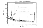
90℃の基板温度で製造された混合層DCV5T:C60の結晶化度の検出:
図1は、DCV5Tフィルム(Si100上)でのX線回折計測(XRD)を示している。純粋なDCV5T層(α,α’−ビス(2,2−ジシアノビニル)キンキチオフェン層)(破線および暗色の実線)はそれぞれ、8.15°および8.65°にピークを示している。ピークは、室温で堆積された試料(RT;暗色の実線)と比較すると、加熱された基板(100℃)に蒸着によって施与された試料の場合(破線)の方がかなり高い。したがって、秩序または結晶化度は100℃試料の場合には、かなり上昇している。結晶化度はC60を含む混合層の場合にはかなり低下している。室温での混合層のスペクトル(RT=室温)は、どこにもピークを示していない。100℃に加熱された基板上への蒸着によって、結晶化度を混合層中でも得ることができるが、ただし、個々の層においてのような良好な結晶化度ではない。この理由は、この場合、ピークが1つしか生じないためである。より良好に判別するために、生じた2つの混合層の曲線プロファイルを、矢印を用いて個々の基板温度に割り当てる。
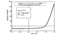
さらなる例示的な実施形態では、構造ITO/p−HTL/HTL/DCV5T:C60/ETL/n−ETL/Alを有するpin型太陽電池を図2で使用する。混合層DCV5T:C60を初めに、90℃の基板温度で(破線の特性曲線、淡色および暗色の特性曲線)、次いで室温で(30℃;実線の特性曲線、淡色および暗色の特性曲線)生じさせる。
ETL:電子輸送層、
HTL:正孔輸送層、
n型ETL:n型ドーピングされた電子輸送層、
p型HTL:p型ドーピングされた正孔輸送層。
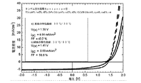
さらなる例示的な実施形態では、構造ITO/n型ETL/ETL/DCV5T:C60/HTL/p型HTL/Auを有するnip型太陽電池を図3で使用している。混合層DCV5T:C60を初めに90℃の基板温度で(破線の特性曲線、淡色および暗色の特性曲線)、次いで、室温で(30℃;実線の特性曲線、淡色および暗色の特性曲線)製造する。
さらなる例示的な実施形態では、構造ITO/ETL/DCV5T:C60/HTL/p型HTL/Auを有するmip型太陽電池を図4で使用する。混合層DCV5T:C60は、90℃の基板温度で製造された(淡色の特性曲線)。mip型構造でも、良好な占有率を有する良好なコンポーネントを実現することができる。
さらなる例示的な実施形態では、異なる層厚の混合層を備えた構造ITO/C60/DCV5T:C60/p型BPAPF/p型ZnPc(p型亜鉛フタロシアニン)/Auを有するmip型太陽電池を図5で使用する。混合層DCV5T:C60を室温で(30℃)製造した。混合層の層厚は10nm(実線の特性曲線、淡色および暗色の特性曲線)および20nm(破線の特性曲線、淡色および暗色の特性曲線)である。
さらなる例示的な実施形態では、異なる層厚の混合層を備えた構造ITO/ETL/DCV5T:C60/HTL/p型HTL/Auを有するmip型太陽電池を図6で使用する。混合層DCV5T:C60を、90℃の基板温度で製造した。混合層の層厚は、10nm(実線の特性曲線、淡色および暗色の特性曲線)および20nm(破線の特性曲線、淡色および暗色の特性曲線)である。
さらなる例示的な実施形態では、混合層ZnPc:C60およびDCV5T:C60を含むpnipnipn型タンデム型電池を図7で使用するが、この場合、これらの混合層を、それぞれ30℃でおよび90℃の基板温度で施与した。このタンデム型電池の構造は、ITO/p型HTL/n型ETL/ETL/ZnPc:C60/p型HTL/n型ETL/ETL/DCV5T:C60/HTL/p型HTL/n型ET/Alである。
Claims (15)
- 電極および対電極ならびに前記電極間の少なくとも1つの有機光活性i型層系を含む有機光活性コンポーネントであって、
(i)前記光活性i型層系が少なくとも1つの混合層を含有し、
(ii)前記混合層が少なくとも1つのドナー材料および少なくとも1つのアクセプター材料を含有し、したがって前記混合層がドナー−アクセプター系を形成しており、
(iii)前記混合層の前記ドナー材料および前記アクセプター材料が非ポリマー材料であり、
(iv)前記ドナー材料が、前記アクセプター材料の蒸発温度よりも少なくとも150℃低い真空中での蒸発温度を有し、
(v)それぞれn型、i型またはp型層系から構成されるnip型、ip型またはni型構造から構成される逆層配列を有し、その際、前記有機光活性i型層系が直接カソード上にまたは電子伝導性n型材料系上に施与されていることを特徴とする、有機光活性コンポーネント。 - 1つまたは複数の層からなるp型および/またはn型材料系を含むことを特徴とする、請求項1に記載の光活性コンポーネント。
- 前記p型および/またはn型材料系が、<450nmの波長範囲に吸収最大を有する1つまたは複数のドーピングされたワイドギャップ層を含有することを特徴とする、請求項1および2のいずれか一つに記載の光活性コンポーネント。
- 入射光の光学的経路を拡大するための光トラップが前記活性系中に形成されていることを特徴とする、請求項1〜3のいずれか一つに記載の光活性コンポーネント。
- ドーピングされたワイドギャップ層が前記i型層に対しては平滑な界面を、かつコンタクトに対しては周期的に微細構造化された界面を有するように、前記光トラップが実現されていることを特徴とする、請求項4に記載の光活性コンポーネント。
- 前記コンポーネントが周期的に微細構造化された基板上に構成されていて、前記コンポーネントの均一な機能、即ち、面全体にわたって短絡のないコンタクト接続および電界の均一な分布が、ドーピングされたワイドギャップ層を使用することによって保証されているという事実によって、前記光トラップが実現されていることを特徴とする、請求項4に記載の光活性コンポーネント。
- 第1の電子伝導層(n型層)と前記基板の上に位置する前記電極との間にp型ドーピングされた層を含有し、その結果、pnip型またはpni型構造が含まれることを特徴とする、請求項1〜6のいずれか一つに記載の光活性コンポーネント。
- 前記光活性i型層と前記基板の上に位置する前記電極との間にp型ドーピングされた層を含有し、その結果、pip型またはpi型構造が含まれ、その際、前記の追加的なp型ドーピングされた層は、前記i型層の電子輸送準位から最高で0.4eV、しかし好ましくは0.3eV未満下に位置するフェルミ準位を有することを特徴とする、請求項1〜7のいずれか一つに記載の光活性コンポーネント。
- 前記p型ドーピングされた層と前記対電極との間にn型層系を含有し、その結果、nipn型またはipn型構造が含まれることを特徴とする、請求項1〜8のいずれか一つに記載の光活性コンポーネント。
- 前記光活性i型層と前記対電極との間にn型層系を含有し、その結果、nin型またはin型構造が含まれ、その際、前記の追加的なn型ドーピングされた層は、前記i型層の正孔輸送準位から最高で0.4eV、しかし好ましくは0.3eV未満に位置するフェルミ準位を有することを特徴とする、請求項1〜9のいずれか一つに記載の光活性コンポーネント。
- n型層系および/またはp型層系を含有し、その結果、pnipn型、pnin型、pipn型またはpin型構造が含まれることを特徴とする、請求項1〜10のいずれか一つに記載の光活性コンポーネント。
- 前記の追加のp型材料系および/または前記の追加のn型材料系が1つまたは複数のドーピングされたワイドギャップ層を含有することを特徴とする、請求項7〜11のいずれか一つに記載の光活性コンポーネント。
- なおさらなるn型層系および/またはp型層系を含有し、その結果、例えばnpnipn型、pnipnp型、npnipnp型、pnpnipnpn型またはpnpnpnipnpnpn型構造が含まれることを特徴とする、請求項1〜12のいずれか一つに記載の光活性コンポーネント。
- 前記のさらなるp型材料系および/または前記のさらなるn型材料系のうちの1つまたは複数が、1つまたは複数のドーピングされたワイドギャップ層を含有することを特徴とする、請求項13に記載の光活性コンポーネント。
- nip型、ni型、ip型、pnip型、pni型、pip型、nipn型、nin型、ipn型、pnipn型、pnin型またはpipn型構造の組み合わせから構成されるタンデム型または多重型(multiple)電池であることを特徴とする、請求項1〜14のいずれか一つに記載の光活性コンポーネント。
Applications Claiming Priority (5)
| Application Number | Priority Date | Filing Date | Title |
|---|---|---|---|
| DE102009024294.5 | 2009-06-05 | ||
| DE102009024294 | 2009-06-05 | ||
| DE102009051142.3A DE102009051142B4 (de) | 2009-06-05 | 2009-10-29 | Photoaktives Bauelement mit invertierter Schichtfolge und Verfahren zu seiner Herstellung |
| DE102009051142.3 | 2009-10-29 | ||
| PCT/EP2010/057889 WO2010139803A1 (de) | 2009-06-05 | 2010-06-07 | Photoaktives bauelement mit invertierter schichtfolge und verfahren zu seiner herstellung |
Publications (2)
| Publication Number | Publication Date |
|---|---|
| JP2012529169A true JP2012529169A (ja) | 2012-11-15 |
| JP2012529169A5 JP2012529169A5 (ja) | 2013-07-04 |
Family
ID=43049417
Family Applications (1)
| Application Number | Title | Priority Date | Filing Date |
|---|---|---|---|
| JP2012513638A Pending JP2012529169A (ja) | 2009-06-05 | 2010-06-07 | 逆層配列を含む光活性コンポーネントおよび前記コンポーネントを製造する方法 |
Country Status (8)
| Country | Link |
|---|---|
| US (1) | US20120125419A1 (ja) |
| EP (1) | EP2438633B1 (ja) |
| JP (1) | JP2012529169A (ja) |
| KR (1) | KR20120034718A (ja) |
| CN (1) | CN102460761A (ja) |
| DE (1) | DE102009051142B4 (ja) |
| ES (1) | ES2879526T3 (ja) |
| WO (1) | WO2010139803A1 (ja) |
Families Citing this family (16)
| Publication number | Priority date | Publication date | Assignee | Title |
|---|---|---|---|---|
| DE102012105812A1 (de) * | 2012-07-02 | 2014-01-02 | Heliatek Gmbh | Elektrodenanordnung für optoelektronische Bauelemente |
| DE102012106607B4 (de) | 2012-07-20 | 2024-04-04 | Heliatek Gmbh | Verfahren zur Versiegelung von Modulen mit optoelektronischen Bauelementen |
| US9660207B2 (en) | 2012-07-25 | 2017-05-23 | Samsung Electronics Co., Ltd. | Organic solar cell |
| DE102012106815A1 (de) | 2012-07-26 | 2014-01-30 | Heliatek Gmbh | Verfahren zur Kontaktierung optoelektronischer Bauelemente |
| US9230339B2 (en) | 2013-01-07 | 2016-01-05 | Wexenergy Innovations Llc | System and method of measuring distances related to an object |
| US9691163B2 (en) | 2013-01-07 | 2017-06-27 | Wexenergy Innovations Llc | System and method of measuring distances related to an object utilizing ancillary objects |
| US8923650B2 (en) | 2013-01-07 | 2014-12-30 | Wexenergy Innovations Llc | System and method of measuring distances related to an object |
| US9845636B2 (en) | 2013-01-07 | 2017-12-19 | WexEnergy LLC | Frameless supplemental window for fenestration |
| US10196850B2 (en) | 2013-01-07 | 2019-02-05 | WexEnergy LLC | Frameless supplemental window for fenestration |
| KR101590574B1 (ko) | 2013-07-31 | 2016-02-01 | 주식회사 엘지화학 | 벌크이종접합 표면 물성의 조절 방법 및 이를 이용한 다층 구조 태양전지 |
| DE102013111164A1 (de) | 2013-10-09 | 2015-05-07 | Heliatek Gmbh | Verfahren zur Herstellung von Kontaktlöchern |
| WO2016045668A1 (de) | 2014-09-26 | 2016-03-31 | Heliatek Gmbh | Verfahren zum aufbringen einer schutzschicht, schutzschicht selbst und halbfabrikat mit einer schutzschicht |
| JP2016106437A (ja) * | 2016-03-17 | 2016-06-16 | 株式会社半導体エネルギー研究所 | 光電変換装置 |
| KR20180081646A (ko) * | 2017-01-06 | 2018-07-17 | 삼성디스플레이 주식회사 | 유기 발광 소자 |
| JP7212037B2 (ja) | 2017-05-30 | 2023-01-24 | ウェクスエナジー リミテッド ライアビリティ カンパニー | 採光用開口のためのフレームレス補助窓 |
| CN110854269B (zh) * | 2019-10-29 | 2021-09-28 | 北京大学 | 一种小分子有机太阳能电池器件及其制备方法 |
Citations (2)
| Publication number | Priority date | Publication date | Assignee | Title |
|---|---|---|---|---|
| WO2008077615A1 (de) * | 2006-12-22 | 2008-07-03 | Novaled Ag | Elektronisches bauelement mit mindestens einer organischen schichtanordnung |
| JP2008532301A (ja) * | 2005-03-04 | 2008-08-14 | へリアテック ゲーエムベーハー | 有機光活性装置 |
Family Cites Families (16)
| Publication number | Priority date | Publication date | Assignee | Title |
|---|---|---|---|---|
| CA1085947A (en) | 1977-08-02 | 1980-09-16 | Ching W. Tang | Multilayer organic photovoltaic elements |
| US5093698A (en) | 1991-02-12 | 1992-03-03 | Kabushiki Kaisha Toshiba | Organic electroluminescent device |
| US5769963A (en) * | 1995-08-31 | 1998-06-23 | Canon Kabushiki Kaisha | Photovoltaic device |
| DE19905694A1 (de) | 1998-11-27 | 2000-08-17 | Forschungszentrum Juelich Gmbh | Bauelement |
| AU2004221377B2 (en) | 2003-03-19 | 2009-07-16 | Heliatek Gmbh | Photoactive component comprising organic layers |
| DE10338406A1 (de) | 2003-08-18 | 2005-03-24 | Novaled Gmbh | Dotierte organische Halbleitermaterialien sowie Verfahren zu deren Herstellung |
| DE10347856B8 (de) | 2003-10-10 | 2006-10-19 | Colorado State University Research Foundation, Fort Collins | Halbleiterdotierung |
| US7061011B2 (en) | 2003-11-26 | 2006-06-13 | The Trustees Of Princeton University | Bipolar organic devices |
| DE10357044A1 (de) | 2003-12-04 | 2005-07-14 | Novaled Gmbh | Verfahren zur Dotierung von organischen Halbleitern mit Chinondiiminderivaten |
| DE102004010954A1 (de) | 2004-03-03 | 2005-10-06 | Novaled Gmbh | Verwendung eines Metallkomplexes als n-Dotand für ein organisches halbleitendes Matrixmaterial, organisches Halbleitermaterial und elektronisches Bauteil |
| DE102005010979A1 (de) | 2005-03-04 | 2006-09-21 | Technische Universität Dresden | Photoaktives Bauelement mit organischen Schichten |
| DE102006053320B4 (de) | 2006-11-13 | 2012-01-19 | Novaled Ag | Verwendung einer Koordinationsverbindung zur Dotierung organischer Halbleiter |
| DE102006054524B4 (de) | 2006-11-20 | 2022-12-22 | Novaled Gmbh | Verwendung von Dithiolenübergangsmetallkomplexen und Selen- analoger Verbindungen als Dotand |
| JP5615174B2 (ja) | 2007-07-23 | 2014-10-29 | ビーエーエスエフ ソシエタス・ヨーロピアBasf Se | 光起電力タンデム電池 |
| DE102008051737B4 (de) | 2007-10-24 | 2022-10-06 | Novaled Gmbh | Quadratisch planare Übergangsmetallkomplexe, organische halbleitende Materialien sowie elektronische oder optoelektronische Bauelemente, die diese umfassen und Verwendung derselben |
| JP5645666B2 (ja) | 2007-10-31 | 2014-12-24 | ビーエーエスエフ ソシエタス・ヨーロピアBasf Se | ハロゲン化フタロシアニン類の使用 |
-
2009
- 2009-10-29 DE DE102009051142.3A patent/DE102009051142B4/de active Active
-
2010
- 2010-06-07 KR KR1020127000392A patent/KR20120034718A/ko not_active Application Discontinuation
- 2010-06-07 US US13/375,597 patent/US20120125419A1/en not_active Abandoned
- 2010-06-07 WO PCT/EP2010/057889 patent/WO2010139803A1/de active Application Filing
- 2010-06-07 ES ES10725079T patent/ES2879526T3/es active Active
- 2010-06-07 EP EP10725079.7A patent/EP2438633B1/de active Active
- 2010-06-07 CN CN2010800248030A patent/CN102460761A/zh active Pending
- 2010-06-07 JP JP2012513638A patent/JP2012529169A/ja active Pending
Patent Citations (2)
| Publication number | Priority date | Publication date | Assignee | Title |
|---|---|---|---|---|
| JP2008532301A (ja) * | 2005-03-04 | 2008-08-14 | へリアテック ゲーエムベーハー | 有機光活性装置 |
| WO2008077615A1 (de) * | 2006-12-22 | 2008-07-03 | Novaled Ag | Elektronisches bauelement mit mindestens einer organischen schichtanordnung |
Also Published As
| Publication number | Publication date |
|---|---|
| EP2438633A1 (de) | 2012-04-11 |
| US20120125419A1 (en) | 2012-05-24 |
| ES2879526T3 (es) | 2021-11-22 |
| WO2010139803A1 (de) | 2010-12-09 |
| KR20120034718A (ko) | 2012-04-12 |
| DE102009051142A1 (de) | 2010-12-09 |
| DE102009051142B4 (de) | 2019-06-27 |
| CN102460761A (zh) | 2012-05-16 |
| EP2438633B1 (de) | 2021-05-26 |
Similar Documents
| Publication | Publication Date | Title |
|---|---|---|
| Chen et al. | Interfacial dipole in organic and perovskite solar cells | |
| JP2012529169A (ja) | 逆層配列を含む光活性コンポーネントおよび前記コンポーネントを製造する方法 | |
| Tonui et al. | Perovskites photovoltaic solar cells: An overview of current status | |
| Wang et al. | Fabrication of efficient metal halide perovskite solar cells by vacuum thermal evaporation: A progress review | |
| JP6310014B2 (ja) | 有機層を含む光活性部品 | |
| Rand et al. | Solar cells utilizing small molecular weight organic semiconductors | |
| DK2398056T3 (en) | Organic solar cell with multiple transportlagsystemer | |
| AU2004221377B2 (en) | Photoactive component comprising organic layers | |
| DK2513995T3 (en) | PHOTOACTIVE COMPONENT WITH ORGANIC LAYERS | |
| Nazeeruddin et al. | Methylammonium lead triiodide perovskite solar cells: A new paradigm in photovoltaics | |
| US10263186B2 (en) | Bulk heterojunction organic photovoltaic cells made by glancing angle deposition | |
| WO2012161773A1 (en) | Organic photovoltaic cell incorporating electron conducting exciton blocking layers | |
| US20120266960A1 (en) | Multi layer organic thin film solar cell | |
| JP6449766B2 (ja) | 光電子デバイス用透明電極 | |
| JP2015523741A (ja) | 電極バッファー層を有する有機光電子デバイスおよびその製造方法 | |
| KR20100046248A (ko) | 질서화된 결정질 유기 막의 성장 방법 | |
| KR102182388B1 (ko) | 와이드 밴드갭을 갖는 페로브스카이트 화합물 막의 후처리 방법 | |
| Kubo | pn-Homojunction Organic Solar Cells | |
| 久保雅之 et al. | pn-Homojunction Organic Solar Cells | |
| Ryan | curves were recorded using a 150 W solar simulator (Abet Technologies) at 1 sun conditions (AM 1.5, 100 mW/cm2). Incident to photon current efficiency (IPCE) studies were carried out using a home-built system utilising a 150 W Oriel Xenon lamp as the light source. | |
| Liu | Doping and Roll-To-Roll Processing of Organic Solar Cells |
Legal Events
| Date | Code | Title | Description |
|---|---|---|---|
| A521 | Request for written amendment filed |
Free format text: JAPANESE INTERMEDIATE CODE: A523 Effective date: 20130516 |
|
| A621 | Written request for application examination |
Free format text: JAPANESE INTERMEDIATE CODE: A621 Effective date: 20130516 |
|
| A977 | Report on retrieval |
Free format text: JAPANESE INTERMEDIATE CODE: A971007 Effective date: 20131211 |
|
| A131 | Notification of reasons for refusal |
Free format text: JAPANESE INTERMEDIATE CODE: A131 Effective date: 20140121 |
|
| A601 | Written request for extension of time |
Free format text: JAPANESE INTERMEDIATE CODE: A601 Effective date: 20140418 |
|
| A602 | Written permission of extension of time |
Free format text: JAPANESE INTERMEDIATE CODE: A602 Effective date: 20140425 |
|
| A521 | Request for written amendment filed |
Free format text: JAPANESE INTERMEDIATE CODE: A523 Effective date: 20140519 |
|
| A02 | Decision of refusal |
Free format text: JAPANESE INTERMEDIATE CODE: A02 Effective date: 20140903 |