JP2012256879A - Ultra-high-speed laser annealing with reduced pattern density effect in manufacture of integrated circuit - Google Patents
Ultra-high-speed laser annealing with reduced pattern density effect in manufacture of integrated circuit Download PDFInfo
- Publication number
- JP2012256879A JP2012256879A JP2012112240A JP2012112240A JP2012256879A JP 2012256879 A JP2012256879 A JP 2012256879A JP 2012112240 A JP2012112240 A JP 2012112240A JP 2012112240 A JP2012112240 A JP 2012112240A JP 2012256879 A JP2012256879 A JP 2012256879A
- Authority
- JP
- Japan
- Prior art keywords
- laser beam
- patterned surface
- laser
- melting
- line image
- Prior art date
- Legal status (The legal status is an assumption and is not a legal conclusion. Google has not performed a legal analysis and makes no representation as to the accuracy of the status listed.)
- Granted
Links
- 238000005224 laser annealing Methods 0.000 title claims abstract description 67
- 230000000694 effects Effects 0.000 title claims abstract description 24
- 238000004519 manufacturing process Methods 0.000 title description 8
- 238000002844 melting Methods 0.000 claims abstract description 181
- 230000008018 melting Effects 0.000 claims abstract description 181
- 238000000034 method Methods 0.000 claims abstract description 92
- 239000000758 substrate Substances 0.000 claims abstract description 27
- 239000002019 doping agent Substances 0.000 claims description 16
- 238000000137 annealing Methods 0.000 claims description 14
- 239000004065 semiconductor Substances 0.000 claims description 12
- 239000002243 precursor Substances 0.000 claims description 9
- 238000010438 heat treatment Methods 0.000 claims description 5
- 239000007787 solid Substances 0.000 claims description 5
- 230000003667 anti-reflective effect Effects 0.000 claims description 3
- 239000002250 absorbent Substances 0.000 claims 1
- 230000002745 absorbent Effects 0.000 claims 1
- 238000006243 chemical reaction Methods 0.000 claims 1
- 235000012431 wafers Nutrition 0.000 description 104
- 239000000155 melt Substances 0.000 description 30
- 230000008569 process Effects 0.000 description 26
- 230000003287 optical effect Effects 0.000 description 22
- XUIMIQQOPSSXEZ-UHFFFAOYSA-N Silicon Chemical compound [Si] XUIMIQQOPSSXEZ-UHFFFAOYSA-N 0.000 description 10
- 229910052710 silicon Inorganic materials 0.000 description 10
- 239000010703 silicon Substances 0.000 description 10
- 238000010521 absorption reaction Methods 0.000 description 7
- 230000004907 flux Effects 0.000 description 7
- 238000009792 diffusion process Methods 0.000 description 4
- 230000006870 function Effects 0.000 description 4
- 238000007654 immersion Methods 0.000 description 4
- 230000008901 benefit Effects 0.000 description 3
- 230000015572 biosynthetic process Effects 0.000 description 3
- 238000004590 computer program Methods 0.000 description 3
- 229910021417 amorphous silicon Inorganic materials 0.000 description 2
- 230000007547 defect Effects 0.000 description 2
- 238000010586 diagram Methods 0.000 description 2
- 238000012986 modification Methods 0.000 description 2
- 230000004048 modification Effects 0.000 description 2
- 238000013021 overheating Methods 0.000 description 2
- 230000035515 penetration Effects 0.000 description 2
- 230000005855 radiation Effects 0.000 description 2
- 230000004044 response Effects 0.000 description 2
- 230000008859 change Effects 0.000 description 1
- 238000005094 computer simulation Methods 0.000 description 1
- 230000008878 coupling Effects 0.000 description 1
- 238000010168 coupling process Methods 0.000 description 1
- 238000005859 coupling reaction Methods 0.000 description 1
- 229910021419 crystalline silicon Inorganic materials 0.000 description 1
- 238000002425 crystallisation Methods 0.000 description 1
- 238000005520 cutting process Methods 0.000 description 1
- 238000010494 dissociation reaction Methods 0.000 description 1
- 230000005593 dissociations Effects 0.000 description 1
- 238000009826 distribution Methods 0.000 description 1
- 238000005516 engineering process Methods 0.000 description 1
- 230000035876 healing Effects 0.000 description 1
- 230000006872 improvement Effects 0.000 description 1
- 230000010354 integration Effects 0.000 description 1
- 230000031700 light absorption Effects 0.000 description 1
- 239000000463 material Substances 0.000 description 1
- 238000010309 melting process Methods 0.000 description 1
- 238000012544 monitoring process Methods 0.000 description 1
- 238000005457 optimization Methods 0.000 description 1
- 230000010287 polarization Effects 0.000 description 1
- 238000012545 processing Methods 0.000 description 1
- 238000005070 sampling Methods 0.000 description 1
- 238000007493 shaping process Methods 0.000 description 1
- 238000003860 storage Methods 0.000 description 1
Images


Classifications
-
- H—ELECTRICITY
- H01—ELECTRIC ELEMENTS
- H01L—SEMICONDUCTOR DEVICES NOT COVERED BY CLASS H10
- H01L21/00—Processes or apparatus adapted for the manufacture or treatment of semiconductor or solid state devices or of parts thereof
- H01L21/02—Manufacture or treatment of semiconductor devices or of parts thereof
- H01L21/04—Manufacture or treatment of semiconductor devices or of parts thereof the devices having at least one potential-jump barrier or surface barrier, e.g. PN junction, depletion layer or carrier concentration layer
- H01L21/18—Manufacture or treatment of semiconductor devices or of parts thereof the devices having at least one potential-jump barrier or surface barrier, e.g. PN junction, depletion layer or carrier concentration layer the devices having semiconductor bodies comprising elements of Group IV of the Periodic System or AIIIBV compounds with or without impurities, e.g. doping materials
- H01L21/30—Treatment of semiconductor bodies using processes or apparatus not provided for in groups H01L21/20 - H01L21/26
- H01L21/324—Thermal treatment for modifying the properties of semiconductor bodies, e.g. annealing, sintering
-
- H—ELECTRICITY
- H01—ELECTRIC ELEMENTS
- H01L—SEMICONDUCTOR DEVICES NOT COVERED BY CLASS H10
- H01L21/00—Processes or apparatus adapted for the manufacture or treatment of semiconductor or solid state devices or of parts thereof
- H01L21/02—Manufacture or treatment of semiconductor devices or of parts thereof
- H01L21/02104—Forming layers
- H01L21/02365—Forming inorganic semiconducting materials on a substrate
- H01L21/02656—Special treatments
- H01L21/02664—Aftertreatments
- H01L21/02667—Crystallisation or recrystallisation of non-monocrystalline semiconductor materials, e.g. regrowth
- H01L21/02691—Scanning of a beam
-
- B—PERFORMING OPERATIONS; TRANSPORTING
- B23—MACHINE TOOLS; METAL-WORKING NOT OTHERWISE PROVIDED FOR
- B23K—SOLDERING OR UNSOLDERING; WELDING; CLADDING OR PLATING BY SOLDERING OR WELDING; CUTTING BY APPLYING HEAT LOCALLY, e.g. FLAME CUTTING; WORKING BY LASER BEAM
- B23K26/00—Working by laser beam, e.g. welding, cutting or boring
- B23K26/02—Positioning or observing the workpiece, e.g. with respect to the point of impact; Aligning, aiming or focusing the laser beam
- B23K26/06—Shaping the laser beam, e.g. by masks or multi-focusing
- B23K26/062—Shaping the laser beam, e.g. by masks or multi-focusing by direct control of the laser beam
- B23K26/0622—Shaping the laser beam, e.g. by masks or multi-focusing by direct control of the laser beam by shaping pulses
-
- B—PERFORMING OPERATIONS; TRANSPORTING
- B23—MACHINE TOOLS; METAL-WORKING NOT OTHERWISE PROVIDED FOR
- B23K—SOLDERING OR UNSOLDERING; WELDING; CLADDING OR PLATING BY SOLDERING OR WELDING; CUTTING BY APPLYING HEAT LOCALLY, e.g. FLAME CUTTING; WORKING BY LASER BEAM
- B23K26/00—Working by laser beam, e.g. welding, cutting or boring
- B23K26/02—Positioning or observing the workpiece, e.g. with respect to the point of impact; Aligning, aiming or focusing the laser beam
- B23K26/06—Shaping the laser beam, e.g. by masks or multi-focusing
- B23K26/073—Shaping the laser spot
- B23K26/0732—Shaping the laser spot into a rectangular shape
-
- H—ELECTRICITY
- H01—ELECTRIC ELEMENTS
- H01L—SEMICONDUCTOR DEVICES NOT COVERED BY CLASS H10
- H01L21/00—Processes or apparatus adapted for the manufacture or treatment of semiconductor or solid state devices or of parts thereof
- H01L21/02—Manufacture or treatment of semiconductor devices or of parts thereof
- H01L21/02104—Forming layers
- H01L21/02365—Forming inorganic semiconducting materials on a substrate
- H01L21/02656—Special treatments
- H01L21/02664—Aftertreatments
- H01L21/02667—Crystallisation or recrystallisation of non-monocrystalline semiconductor materials, e.g. regrowth
- H01L21/02675—Crystallisation or recrystallisation of non-monocrystalline semiconductor materials, e.g. regrowth using laser beams
- H01L21/02678—Beam shaping, e.g. using a mask
-
- H—ELECTRICITY
- H01—ELECTRIC ELEMENTS
- H01L—SEMICONDUCTOR DEVICES NOT COVERED BY CLASS H10
- H01L21/00—Processes or apparatus adapted for the manufacture or treatment of semiconductor or solid state devices or of parts thereof
- H01L21/02—Manufacture or treatment of semiconductor devices or of parts thereof
- H01L21/02104—Forming layers
- H01L21/02365—Forming inorganic semiconducting materials on a substrate
- H01L21/02656—Special treatments
- H01L21/02664—Aftertreatments
- H01L21/02667—Crystallisation or recrystallisation of non-monocrystalline semiconductor materials, e.g. regrowth
- H01L21/02675—Crystallisation or recrystallisation of non-monocrystalline semiconductor materials, e.g. regrowth using laser beams
- H01L21/02683—Continuous wave laser beam
-
- H—ELECTRICITY
- H01—ELECTRIC ELEMENTS
- H01L—SEMICONDUCTOR DEVICES NOT COVERED BY CLASS H10
- H01L21/00—Processes or apparatus adapted for the manufacture or treatment of semiconductor or solid state devices or of parts thereof
- H01L21/02—Manufacture or treatment of semiconductor devices or of parts thereof
- H01L21/02104—Forming layers
- H01L21/02365—Forming inorganic semiconducting materials on a substrate
- H01L21/02656—Special treatments
- H01L21/02664—Aftertreatments
- H01L21/02667—Crystallisation or recrystallisation of non-monocrystalline semiconductor materials, e.g. regrowth
- H01L21/02675—Crystallisation or recrystallisation of non-monocrystalline semiconductor materials, e.g. regrowth using laser beams
- H01L21/02686—Pulsed laser beam
-
- H—ELECTRICITY
- H01—ELECTRIC ELEMENTS
- H01L—SEMICONDUCTOR DEVICES NOT COVERED BY CLASS H10
- H01L21/00—Processes or apparatus adapted for the manufacture or treatment of semiconductor or solid state devices or of parts thereof
- H01L21/02—Manufacture or treatment of semiconductor devices or of parts thereof
- H01L21/04—Manufacture or treatment of semiconductor devices or of parts thereof the devices having at least one potential-jump barrier or surface barrier, e.g. PN junction, depletion layer or carrier concentration layer
- H01L21/18—Manufacture or treatment of semiconductor devices or of parts thereof the devices having at least one potential-jump barrier or surface barrier, e.g. PN junction, depletion layer or carrier concentration layer the devices having semiconductor bodies comprising elements of Group IV of the Periodic System or AIIIBV compounds with or without impurities, e.g. doping materials
- H01L21/22—Diffusion of impurity materials, e.g. doping materials, electrode materials, into or out of a semiconductor body, or between semiconductor regions; Interactions between two or more impurities; Redistribution of impurities
- H01L21/223—Diffusion of impurity materials, e.g. doping materials, electrode materials, into or out of a semiconductor body, or between semiconductor regions; Interactions between two or more impurities; Redistribution of impurities using diffusion into or out of a solid from or into a gaseous phase
-
- H—ELECTRICITY
- H01—ELECTRIC ELEMENTS
- H01L—SEMICONDUCTOR DEVICES NOT COVERED BY CLASS H10
- H01L21/00—Processes or apparatus adapted for the manufacture or treatment of semiconductor or solid state devices or of parts thereof
- H01L21/02—Manufacture or treatment of semiconductor devices or of parts thereof
- H01L21/04—Manufacture or treatment of semiconductor devices or of parts thereof the devices having at least one potential-jump barrier or surface barrier, e.g. PN junction, depletion layer or carrier concentration layer
- H01L21/18—Manufacture or treatment of semiconductor devices or of parts thereof the devices having at least one potential-jump barrier or surface barrier, e.g. PN junction, depletion layer or carrier concentration layer the devices having semiconductor bodies comprising elements of Group IV of the Periodic System or AIIIBV compounds with or without impurities, e.g. doping materials
- H01L21/26—Bombardment with radiation
- H01L21/263—Bombardment with radiation with high-energy radiation
- H01L21/268—Bombardment with radiation with high-energy radiation using electromagnetic radiation, e.g. laser radiation
Abstract
Description
本開示は、概して、半導体製造において集積回路を形成する際に用いられるアニーリングに関し、とりわけ、集積回路の形成においてパターン密度効果を低減させる超高速レーザーアニーリングに関する。 The present disclosure relates generally to annealing used in forming integrated circuits in semiconductor manufacturing, and more particularly to ultrafast laser annealing that reduces pattern density effects in the formation of integrated circuits.
従来のナノ秒パルスレーザー溶融アニーリング(従来の溶融レーザーアニーリング)は、高度な集積回路(IC)チップ製造に理想的な、超低熱量、高ドーパント活性、および極めて高いステップ接合を有するといわれている。しかしながら、実際には、ICチップの光学的および熱的な特性の空間変動に起因する温度不均一性により、このタイプのアニーリングを回路パターン付きウエハに適用して実施するのは難しい。この温度不均一性は、当技術分野において「パターン密度効果」と呼ばれる。 Conventional nanosecond pulsed laser melt annealing (conventional melt laser annealing) is said to have ultra-low heat, high dopant activity, and extremely high step bonding, ideal for advanced integrated circuit (IC) chip manufacturing . In practice, however, this type of annealing is difficult to implement on circuit patterned wafers due to temperature non-uniformities due to spatial variations in the optical and thermal characteristics of the IC chip. This temperature non-uniformity is referred to in the art as the “pattern density effect”.
吸収層あるいは位相スイッチ層を用いることによってパターン密度効果を軽減することができる。この吸収層は、光学的吸収均一性を大いに向上させることができるが、不均一な熱的特性によるパターン密度効果によって、プロセスウィンドウは依然として制限される。とりわけ、ナノ秒パルス持続時間に関係する短い熱拡散長さ(〜1μm)は、製造中のICチップの材料特性における空間変動を平均化するのに十分ではない。 By using the absorption layer or the phase switch layer, the pattern density effect can be reduced. This absorbing layer can greatly improve the optical absorption uniformity, but the process window is still limited by pattern density effects due to non-uniform thermal properties. In particular, the short thermal diffusion length (˜1 μm) related to nanosecond pulse duration is not sufficient to average the spatial variation in the material properties of the IC chip being manufactured.
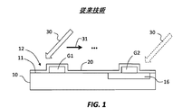
例えば、図1には、回路パターン付き基板表面12を支持する表面11を有するシリコン基板(ウエハ)10の一部の概略断面が示されており、当該パターン付き表面には、従来の溶融レーザーアニーリングが施されている。パターン付き基板表面12は、基板表面11に形成された第1のポリゲートG1、および基板表面11に形成されたフィールド酸化膜領域16の表面に形成された第2のポリゲートG2を有している。これら2つのポリゲートG1およびG2を覆う吸収キャップ層20が形成されている。従来のレーザーアニーリングビーム30は、矢印31の方向にウエハ10を走査するとともに、2つのポリゲートG1およびG2を加熱する。
For example, FIG. 1 shows a schematic cross-section of a portion of a silicon substrate (wafer) 10 having a
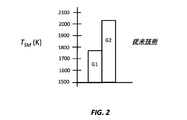
図2は、従来の溶融レーザーアニーリング処理のコンピュータシミュレーションによって算出された、回路パターン付きウエハ表面12のポリゲートG1およびG2における最大表面温度TSM(K)の棒グラフである。図2によれば、キャップされたポリゲートG2は、その下側に設けられた熱伝導率の低いフィールド酸化膜領域16のために、シリコンウエハに直接的に設けられたポリゲートG1と比較して、過度に熱せられていることが解る。図2の棒グラフは、パターン密度効果に起因する過熱が従来の溶融レーザーアニーリング処理よりも200℃以上高いことを示している。位置スイッチ層を設けることにより、過熱領域において光の吸収の自己調節が働き、パターン密度効果の有る程度の軽減が可能となる。しかしながら、このような位相スイッチ層の使用は、実質的に、プロセスの煩雑さを招くとともに、コストアップの要因となる。
FIG. 2 is a bar graph of the maximum surface temperature T SM (K) at the polygates G1 and G2 on the circuit-patterned
本発明の一側面は、回路パターンが付された表面および或る溶融温度を有する半導体基板のアニーリング方法である。この方法では、少なくとも一つの第1レーザービームで当該パターン付き表面を走査し、この少なくとも一つの第1レーザービームで、パターン付き表面を当該溶融温度から約400℃低い温度以内の非溶融温度Tnonmeltまで加熱する。さらにこの方法では、少なくとも一つの第2レーザービームでパターン付き表面を走査する工程を有している。少なくとも一つの第2レーザービームは、パルス状で、かつ、非溶融温度から溶融温度までパターン付き表面を加熱するようになっている。 One aspect of the present invention is a method for annealing a semiconductor substrate having a surface with a circuit pattern and a certain melting temperature. In this method, the patterned surface is scanned with at least one first laser beam, and the patterned surface is scanned with the at least one first laser beam at a non-melting temperature T nonmelt within about 400 ° C. below the melting temperature . Until heated. The method further includes scanning the patterned surface with at least one second laser beam. At least one second laser beam is pulsed and heats the patterned surface from a non-melting temperature to a melting temperature.
本発明の他の側面は、パターン付き表面および或る溶融温度を有する半導体基板のレーザーアニーリングを行うシステムである。当該システムは、少なくとも一つの第1レーザービームを生成するとともに、この少なくとも一つの第1レーザービームでパターン付き表面の走査を行うものである。少なくとも一つの第1レーザービームは、溶融温度から約400℃以内にある非溶融温度Tnonmeltまでパターン付き表面を加熱する。また、このシステムは、少なくとも一つの第2レーザービームを生成するとともに、第1レーザービームと関連して、この少なくとも一つの第2レーザービームで走査を行うものである。少なくとも一つの第2レーザービームは、パルス状(すなわち、光パルスから成っている)であり、かつ、非溶融温度から溶融温度までパターン付き表面を加熱するようになっている。 Another aspect of the present invention is a system for laser annealing of a patterned substrate and a semiconductor substrate having a certain melting temperature. The system generates at least one first laser beam and scans the patterned surface with the at least one first laser beam. The at least one first laser beam heats the patterned surface to a non-melt temperature T nonmelt that is within about 400 ° C. from the melt temperature. The system also generates at least one second laser beam and scans with the at least one second laser beam in association with the first laser beam. The at least one second laser beam is pulsed (ie, consists of light pulses) and is adapted to heat the patterned surface from a non-melting temperature to a melting temperature.
本発明のさらに別の側面は、パターン付き表面を有する半導体基板のレーザーアニーリング方法である。この方法は、パターン付き表面の許容できる温度ムラΔTを選択する工程を含んでいる。この方法は、さらに、下記の関係による、最小非溶融温度Tnonmeltを決定する工程を含んでいる。

本発明の付加的な特徴および長所は、後述する詳細な説明に明記されている。また、それらの一部は、詳細な説明の記載内容から当業者にとって直ちに明白となるか、下記の詳細な説明、特許請求の範囲、添付図面を含む、ここに記載された実施形態を実施することによって認識される。 Additional features and advantages of the invention are set forth in the detailed description below. Some of them will be readily apparent to those skilled in the art from the detailed description, or may be implemented with the embodiments described herein, including the following detailed description, the claims, and the accompanying drawings. Is recognized by
上記の背景技術に関する記載および下記の本発明の詳細な説明に関する記載は、特許請求の範囲に記載されているように、本発明の本質および特徴を理解するための概略または枠組みを提供するものであることを理解すべきである。添付図面は、本発明のさらなる理解を提供するために含まれており、本明細書に組み込まれ、本明細書の一部を構成する。図面は、本発明の様々な実施形態を図示するものであり、本明細書の記載とともに、本発明の原則および実施を説明する一助となる。特許請求の範囲は、本明細書に組み込まれ、本明細書の一部を構成する。 The foregoing description of the background art and the following detailed description of the invention, as set forth in the claims, provide an overview or framework for understanding the nature and characteristics of the invention. It should be understood. The accompanying drawings are included to provide a further understanding of the invention, and are incorporated in and constitute a part of this specification. The drawings illustrate various embodiments of the invention and together with the description serve to explain the principles and practice of the invention. The claims are hereby incorporated into and constitute a part of this specification.
ここで、本発明の様々な実施形態を詳細に参照する。実施形態の一例を図面に示す。図中、同一または同様の部分を参照する際、可能な限り同一または同様の参照番号及び符号を使用する。図面には決まった縮尺が無く、当業者であれば、これら図面は本発明の主要な部分を説明するために簡略化されていることに気づくであろう。いくつかの図面において、参考のために直交座標系が描かれているが、これは特定の方向および当該システムや方法の配置方向を限定するものではない。特許請求の範囲に記載された内容は、本明細書に組み込まれて援用される。 Reference will now be made in detail to various embodiments of the invention. An example of an embodiment is shown in the drawings. In the drawings, the same or similar reference numerals and symbols are used as much as possible when referring to the same or similar parts. The drawings are not to scale and those skilled in the art will recognize that these drawings have been simplified to illustrate the major portions of the present invention. In some of the drawings, an orthogonal coordinate system is drawn for reference, but this does not limit the particular direction and orientation of the system or method. The contents described in the claims are incorporated and incorporated herein by reference.
「半導体基板」および「ウエハ」の語は、互いに同じ意味であり、互いに入れ替えて使用可能に用いられている。同様に、「基板表面」および「ウエハ表面」の語も、互いに同じ意味であり、互いに入れ替えて使用可能である。さらに、「半導体基板表面」の語は、「基板表面」と短縮される。集積回路デバイスの製造等に用いられる「半導体ウエハ」の語は、「ウエハ」と短縮される。「ウエハ」の典型例は、シリコンウエハである。明細書および図面にて使用される「K」の文字は、「度ケルビン」の意味である。 The terms “semiconductor substrate” and “wafer” have the same meaning and are used interchangeably. Similarly, the terms “substrate surface” and “wafer surface” have the same meaning and can be used interchangeably. Further, the term “semiconductor substrate surface” is abbreviated as “substrate surface”. The term “semiconductor wafer” used for manufacturing integrated circuit devices is abbreviated as “wafer”. A typical example of a “wafer” is a silicon wafer. The letter “K” used in the specification and drawings means “degree Kelvin”.
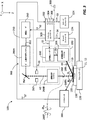
図3は、本発明が適用された超高速レーザーアニーリングシステム(以下、単に「システム」という)100の一例を示す概略図である。システム100は、チャック上面132を有するチャック130を使用可能に支持するウエハステージ120を有している。ウエハステージ120は、X−Y平面で可動する(Z方向を加えてもよい)。チャック上面132は、回路パターン付きウエハ表面12(以下、「ウエハ表面12」または「基板表面12」という)が形成された平面11を有するウエハ10を使用可能に支持する。ウエハ表面12の例を図4D、図6Aから図6Dに示す。ここで、ウエハ表面12は、ICチップの製造に用いられる様々なステージに合わせて、単なる平坦な平面11に限らず、任意の形状をとり得る。
FIG. 3 is a schematic diagram showing an example of an ultrafast laser annealing system (hereinafter simply referred to as “system”) 100 to which the present invention is applied. The
一例において、ウエハ10をプレヒートするために、チャック13が加熱される。ウエハステージ120は、ウエハステージコントローラ124に使用可能に接続されており、チャック130は、チャックコントローラ134に使用可能に接続されている。
In one example, the chuck 13 is heated to preheat the
システム100は、ウエハ表面温度TSを上げるウエハ表面12のプレヒートに使用される少なくとも1つの第1レーザービーム168を生じさせる第1レーザーシステム150を備えている。ウエハ表面温度TSは、一例として、ウエハ溶融温度Tmeltよりも約50℃低い温度から、ウエハ溶融温度Tmeltよりも約400℃低い温度までの範囲である。したがって、以下において、第1レーザーシステム150は、非溶融レーザーシステム150であり、また、少なくとも1つの第1レーザービームは、少なくとも1つの非溶融レーザービーム168である。
The
非溶融レーザーシステム150は、非溶融レーザー160と、第1光学軸A1を規定する非溶融光学システム166とを有している。この非溶融レーザー160は、ダイオードレーザー、あるいは、P極偏向した10.6ミクロンのCO2レーザーの連続波(CW)といった、CO2レーザーを含む。軸A1は、非溶融レーザービーム168がウエハ表面12に対してほぼ垂直の入射角θ1あるいは大きな斜めの入射角θ1となるように方向が規定される。実施例において、第1光学軸A1は、ウエハ表面12のブルースター角(偏光角)と実質的に等しい角度θ1を有しており、前述の、不均一な光学的吸収によるパターン密度効果が軽減あるいは極小化される。
The
非溶融光学システム166は、最初の非溶融レーザービーム162を受け入れるとともに、当該ビーム162から非溶融レーザービーム168を形成する。非溶融レーザービーム168は、第1(非溶融)光学軸A1に沿って進み、ウエハ表面12に第1(非溶融)ラインイメージ170を形成する。
The non-melting
図4Aは、ウエハ表面12上に形成された理想的な非溶融ラインイメージ170の一例についての概略平面図である。図4Bおよび図4Cは、非溶融ラインイメージ170を形成する非溶融レーザービームの一例の強度プロファイル170Pの概略グラフであり、図4BはY方向、図4CはX方向に取り込んだものである。非溶融レーザービームの強度プロファイル170Pは、ウエハ表面12における非溶融レーザービーム168のそれに対応するとともに、例えばある程度の閾強度ITHよりも大きな強度によって非溶融ラインイメージ170を決定する。非溶融ラインイメージ170は、走査方向(すなわち、X方向)に直交する長手方向(すなわち、Y方向)のセンターラインあるいは軸C1を有している。非溶融ラインイメージ170は、図4Aにおいて大きな矢印で示されるように、速度VSでX方向に走査される。
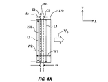
FIG. 4A is a schematic plan view of an example of an ideal
典型的な非溶融レーザービーム168は、当該走査方向においてガウス強度プロファイルを有しており、また、長手方向(走査方向に交差する方向)において相対的に平らなプロファイルを有している。非溶融レーザービーム168(非溶融ラインイメージ170)のビーム幅W1(上記ガウスプロファイルにおける最大値の半分の幅(FWHM)が最大幅として決定されている)の一例は、約0.05mmから約2mmの範囲にある。非溶融レーザービーム168(つまり非溶融ラインイメージ170)の一例のビーム長さL1は、典型的には、約5mmから約20mmの範囲にある。一例において、非溶融レーザービーム168およびこれに対応する非溶融ラインイメージ170の走査には、約30ミクロンから約500ミクロンの範囲の、ウエハ10に関連する熱拡散長さ(深さ)がある。
A typical
図3を再び参照するに、システム100は、少なくとも1つの第2レーザービーム268を生成する第2レーザーシステム250を有している。この少なくとも1つの第2レーザービーム268は、ウエハ表面10における、非溶融レーザービーム168が照射されることによって(また加熱されたチャック130を用いても良い)プレヒートされる部分にさらに熱を加えて局所的なウエハ表面温度TSをウエハ溶融温度Tmeltまで上げるのに用いられる。これにより、ウエハ表面12は局所的に溶融する。したがって、以下では、第2レーザーシステム250を、溶融レーザーシステム250という。また、少なくとも1つの第2レーザービーム268を、少なくとも1つの溶融レーザービーム268という。
Referring back to FIG. 3, the
一例において、溶融レーザーシステム250は、一連の溶融光パルス262Pを含む最初の溶融レーザービーム262を生成する溶融レーザー260を有している。溶融レーザーシステム250は、さらに、第2(溶融)光学軸A2に沿って溶融レーザー260との関係で使用可能に配置された溶融光学システム266を有している。溶融光学システム266の一例は、ビーム整形光学システム266A、折り返しミラーFM、調整可能なアパーチャー267、および投影光学システム266Bを有している。溶融光学システム266は、溶融レーザー260からの最初の溶融パルスレーザービーム262を受けるとともに、当該レーザービーム262から溶融レーザービーム268(光パルス268Pを含む)を生成する。溶融レーザービーム268は、前述のように、ウエハ表面の局所を溶融させるため、非溶融ラインイメージ170との関係で、ウエハ表面12において第2(溶融)ラインイメージ270を形成する。実施例では、図3に示すように、第2(溶融)光学軸A2は、実質的にウエハ表面12に対して垂直の入射角度θ2を有しているが、第2光学軸A2の入射角度θ2は、どのような値であってもよい(入射角度θ2は、図6Aを参照のこと)。
In one example, the
図4Aは、非溶融ラインイメージ170に相対してウエハ表面12上に形成された理想溶融ラインイメージ270の一例についての概略平面図を含んでいる。図4Bおよび図4Cは、溶融レーザービーム268の一例の強度プロファイル270PをX方向およびY方向に切り取った断面グラフを含んでいる。強度プロファイルは、例えば閾強度ITHよりも大きな強度によって、溶融ラインイメージ270を形成する。溶融ラインイメージ270は、Y方向の長さL2と、X方向の幅W2とを有している。
FIG. 4A includes a schematic plan view of an example ideal
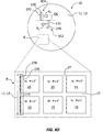
図4Dは、ウエハ表面12の領域Rの一例を示す拡大差込図を含む、ウエハ10の一例についての平面図である。領域Rは、隙間17によって離間配置された多数のICチップ15を含んでいる。この隙間17は、例えば、ひき目を入れた領域でもよいし、ICチップを切り出す際のけがき線を構成する領域であってもよい。一例において、溶融ラインイメージ270の長さL2は、非溶融ラインイメージ170および溶融ラインイメージ270による互いに隣り合う走査SC1およびSC2の接触が隙間17内で生じるように、レーザーアニールされる具体的な集積回路(IC)チップ15と同じか数倍にすることができる。図4Dにおける点線DLは、隣り合う走査SC1およびSC2が触れ合う位置を示している。
FIG. 4D is a plan view of an
一例において、少なくとも一つの非溶融ラインイメージの長さL1および溶融ラインイメージの長さL2は、ウエハ表面12上の、ICチップ15によって決定される選択領域Rに溶融処理を限定するように設定される。溶融光パルス268Pのタイミングを制御することにより、走査方向における選択的な溶融を行うことができる。ICチップ15とは、現に製造プロセス中のチップであってもよく、ICチップに仕上げられている必要はない。換言すれば、ICチップ15は、完成されたICチップが形成される部分を含む意味である。
In one example, the length L1 of the at least one non-melting line image and the length L2 of the melting line image are set to limit the melting process to a selected area R determined by the
走査方向に沿った強度プロファイル270Pは、平坦な形状あるいは湾曲した形状(例えばガウス分布)のいずれであってもよい。一例において、溶融ラインイメージ270の幅W2は、強度プロファイル270Pの直交座標のY方向にけるFWHMによって決定される。平らな溶融レーザーの典型的な幅W2は、10ミクロンから500ミクロンの範囲にある。一例において、溶融ラインイメージ270の長さL2は、実質的に非溶融ラインイメージ170の長さL1と同じである。溶融ラインイメージ270の平らな強度プロファイル270Pの方が一般にエネルギー効率が良いと考えられる。
The
図5は、温度T(K)と位置(mm)との関係を示すグラフであり、非溶融レーザービーム168の走査およびウエハ表面12上の対応する非溶融ラインイメージ170によって形成されたウエハ表面温度プロファイルの一例の温度カーブTC1を示している。非溶融レーザービーム強度プロファイル170Pが適切な位置関係で同グラフ上に重ね合わされている。このグラフは、非溶融レーザービーム強度プロファイル170Pの最大強度IMAXNMの位置と、ピーク温度線としての軸PTLで示される最大表面温度TSMの位置との間に、位置的な差Δxがあることを示している。この位置的な差Δxを「ポジショナルラグ」という。なお、走査方向は、X方向である。
FIG. 5 is a graph showing the relationship between temperature T (K) and position (mm), the wafer surface temperature formed by scanning the
図5に示すように、ウエハ表面温度の均一性は良好である。溶融ラインイメージ270のセンターラインあるいは軸C2は、実質的に、非溶融加熱に関連するピーク温度ライン(軸)PTLに沿って設定されている。ポジショナルラグΔxは、ステージ速度VSおよび非溶融レーザービーム168の幅W1に依存して、走査方向における数ミクロンから数百ミクロンの範囲をとることができる。
As shown in FIG. 5, the uniformity of the wafer surface temperature is good. The center line or axis C2 of the
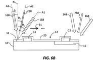
図6Aは、図1と同様の図であるが、図6Aは、超高速レーザーアニーリング処理が1つの非溶融レーザービーム168と1つの溶融レーザービーム268とを用いて実施される例を示している。ウエハ表面12への法線は、破線Nで示されている。溶融レーザービーム268の入射角θ2は、(図示の通り)ほぼ直角、あるいはやや傾いている。もし、ほぼ直角(すなわち、直角から30°以内)であれば、円偏光した溶融レーザー260を使用して、前述のパターン密度効果を軽減あるいは極小化することができる。ある種の高度な集積回路の製造に際し、回路パターンを形成する線は、一般的に、レーザー波長よりも十分に小さく、また、当該線は、一方向を指向している。この場合において、P偏光した溶融レーザービーム268は、相対的に大きな入射角θ2(例えば、50°から75°の範囲)で使用することができる。結果として、入射面は、パターン線に対して直交する。一例において、非溶融レーザービーム168の入射角θ1は、一般的に、0°(垂直入射)から90°までのいずれでもよい。前述のブルースター角を選択するのが好適である。
FIG. 6A is a view similar to FIG. 1, but FIG. 6A shows an example where an ultrafast laser annealing process is performed using one
図6Bは、図6Aと同様の図であり、2本の非溶融レーザービーム168を利用する超高速アニーリング方法の一例を示している。このケースにおいて、1本の非溶融レーザービーム168は、ウエハ表面12を中間温度まで加熱するのに使用され、他の非溶融レーザービームは、当該表面の温度をウエハ溶融温度Tmeltの近くまで上げるのに使用される。この方法によれば、超高速アニーリングプロセスの最適化について、さらなる柔軟性を与えることができる。
FIG. 6B is a diagram similar to FIG. 6A and shows an example of an ultrafast annealing method using two
溶融レーザー260に関して、光結合効率を向上させ、さらに、パターン密度効果をより軽減させるため、図6Cには、誘電性反射防止層21をウエハ表面12上に積層して、浅い溝状の絶縁領域における過熱を防止しつつ、むき出しのシリコン領域における出力溶融レーザービーム268の吸収を向上させる例が示されている。
In order to improve the optical coupling efficiency with respect to the
本発明にかかる超高速レーザーアニーリングシステムおよび方法は、パターン密度効果を軽減する現在の他の技術と組み合わせて実施することができる。現在の技術には、例えば、吸収キャップ層20(半透明あるいは不透明のもの。図6Aおよび図6Bを参照)を使用すること、あるいは、反射防止層(図6C)を使用して加熱の均一性をさらに向上させること(図6Aおよび図6B)が挙げられる。あるいは、図6Dに示すように、本発明にかかる超高速レーザーアニーリングシステムおよび方法を、追加的な技術あるいは介在媒体なしに、ウエハ表面12に直接的に適用してもよい。
The ultrafast laser annealing system and method according to the present invention can be implemented in combination with other current technologies that reduce pattern density effects. Current techniques include, for example, using an absorbing cap layer 20 (translucent or opaque, see FIGS. 6A and 6B) or heating uniformity using an anti-reflective layer (FIG. 6C). Is further improved (FIGS. 6A and 6B). Alternatively, as shown in FIG. 6D, the ultrafast laser annealing system and method according to the present invention may be applied directly to the
溶融レーザービーム268の波長の選択は、レーザーアニーリングを具体的に何に対して適用するかによる。高度なトランジスタ製造に用いられる超浅接合形成において、溶融深さは、典型的には、数ナノメーターから数十ナノメーターの範囲になる。このため、ウエハ10への貫通深さを制限するために、光学的吸収効率の高い短波長溶融レーザー260を用いてもよい。溶融レーザー260に用いられるレーザーの例として、エキシマレーザー(例えば、308nmのXeClエキシマレーザー)および532nmの固体レーザーを挙げることができる。比較的深い溶融が必要なレーザーアニーリングには、実質的に光学的貫通深さを有するIRレーザー(1064nmのNd:YAGレーザー、あるいはCO2レーザー等)を溶融レーザー260として使用できる。
The selection of the wavelength of the melted
一例において、溶融レーザー260の繰返し率は、溶融レーザーラインイメージ270の走査方向幅W1でステージ走査速度を除した値よりも大きい。これにより、走査されたウエハ表面12上の各点が溶融レーザー260からの少なくとも1本の溶融光パルス268Pを確実に受けるようにすることができる(すなわち、隣合う溶融ラインイメージ270が少なくとも互いに触れ合うことになる。)。溶融レーザー260の繰返し率は、一例として1kHz以上であり、他の例としては、1kHzから100kHzの範囲を挙げることができる。一例において、溶融レーザービーム268におけるパルス268Pの時間幅ΔtMは、約5nsから約1μsの範囲にある(図3参照)。ウエハステージ120の速度の一例は、10mm/sから1000mm/sの範囲にあり、溶融ラインイメージ270の典型的な幅W2は、約100ミクロンである。一例において、溶融レーザー260は、20Wから500Wの範囲の出力を有する溶融レーザービーム268を生成する。
In one example, the repetition rate of the
図3を再び参照するに、システム100は、ウエハ表面温度を測定するとともに、測定されたウエハ表面温度TSの代表値としての温度信号STを生成するパイロメータ280をさらに備えることができる。
Referring back to FIG. 3, the
システム100は、さらに、ウエハステージコントローラ124に電気的に接続されたシステムコントローラ300と、チャックコントローラ134と、非溶融レーザー160と、溶融レーザー260と、調整可能なアパーチャー267と、パイロメータ280とを備えている。一例において、システムコントローラ300は、当該コントローラにシステム100における様々なコンポーネントを操作させるために(例えば、コンピュータ等の機器が判読可能な媒体に記録されたソフトウェアのような命令群によって)適用されるコンピュータ等の機器を有している。システムコントローラ300は、プロセッサユニット(プロセッサ)302およびメモリユニット(メモリ)304を有している。一例にかかるコントローラ300は、プロセッサを含むコンピュータであり、または当該コンピュータを含み、マイクロソフト社のウィンドウズ(登録商標)あるいはリナックス(登録商標)といったオペレーションシステムを含む。
The
実施例において、プロセッサ302は、一連のソフトウェア命令を実行可能な任意のプロセッサあるいはデバイス、あるいはこれらを有するものであり、特段の制限はなく、汎用あるいは特定用途向けのマイクロプロセッサ、有限状態機械、コントローラ、コンピュータ、中央演算処理装置(CPU)、フィールド・プログラマブル・ゲート・アレイ(FPGA)、あるいはデジタル・シグナル・プロセッサを用いることができる。実施例において、当該プロセッサは、インテル社のXeonあるいはPENTIUM(登録商標)プロセッサ、AMD社のTURION(登録商標)、あるいはAMD社、インテル社、そのほかの半導体プロセッサメーカ製のプロセッサを用いることができる。
In an embodiment, the
メモリ304は、プロセッサ302に使用可能に接続されている。ここで、「メモリ」の語は、プロセッサが判読可能なすべての媒体を意味しており、RAM、ROM、EPROM、PROM、EEPROM、ディスク、フレキシブルディスク、ハードディスク、CD−ROM、DVD等を含む(これらに限定されるものではない)、プロセッサ302によって実行される一連の命令が記憶されるものである。実施例において、システムコントローラ300は、CD−ROM、DVE、メモリースティック他の記憶媒体といった、取り外し可能かつプロセッサが判読可能な媒体308を収容するために適用されたディスクドライブ306を含んでいる。
本発明にかかるアニーリング方法をシステム100の運転制御によってシステムコントローラ300に実行させるための、機械的に判読可能な命令(例えば、コンピュータプログラムおよび/またはソフトウェアモジュール等)が記憶された機械判読可能な媒体(例えば、メモリ302)において、本発明にかかる超高速レーザーアニーリング方法の様々な実施例を実行させてもよい。実施例において、コンピュータプログラムは、メモリ304の外のプロセッサ302上で実行される。
A machine-readable medium storing a machine-readable instruction (for example, a computer program and / or a software module) for causing the
コンピュータプログラムおよび/またはソフトウェアモジュールは、本発明にかかる様々な方法を実施するとともに、システム100における様々なコンポーネントの運転および機能を制御する複数のモジュールあるいはオブジェクトを備えることができる。当該コードに用いられるコンピュータプログラミング言語の種類は、手続き型言語からオブジェクト指向言語までの様々な言語を使用することができる。各ファイルあるいはオブジェクトは、各モジュールあるいは方法のステップと一対一に対応する必要はない。さらに、方法および装置は、ソフトウェア、ハードウェア、およびファームウェアを組み合わせたものであってもよい。本発明にかかる様々な実施例を実行するため、ファームウェアがプロセッサ302にダウンロードされ得る。
A computer program and / or software module may comprise multiple modules or objects that perform various methods in accordance with the present invention and control the operation and function of various components in
システムの運転
システム100の運転の例において、システムコントローラ300が第1の制御信号S1を非溶融レーザー160に送信すると、これに応答して、非溶融レーザー160は、最初の非溶融レーザービーム162を生成する。この最初の非溶融レーザービーム162は、非溶融光学システム166に受け入れられ、ここで非溶融レーザービーム168が形成される。非溶融レーザービーム168は、第1光学軸A1に沿って進み、ウエハ表面12において非溶融ラインイメージ170を形成する。
System Operation In the
さらに、システムコントローラ300が第2の制御信号S2を溶融レーザー260に送信すると、これに応答して、溶融レーザー260は、最初の溶融レーザービーム262を生成する。この最初の溶融レーザービーム262は、溶融光学システム266に受け入れられ、ここで、非溶融ラインイメージ170との関係で溶融ラインイメージ270を形成し、前述の、ウエハ表面を局所的に溶融する出力溶融パルスレーザービーム268が形成される。
Further, when the
さらに、システムコントローラ300は、非溶融ラインイメージ170および溶融ラインイメージ270に応じてウエハ10を動かす(走査する)ウエハステージコントローラ124に第3の制御信号S3を送信する。チャック130がウエハのプレヒートを行う実施例において、システムコントローラ300は、制御信号S4をチャックコントローラ134に送信し、ウエハのプレヒート処理を開始させるようにしてもよい。一例において、システムコントローラ300は、さらに、パイロメータ280から温度信号STを受け入れるとともに、この温度信号を、非溶融レーザービーム168および溶融レーザービーム268の一方あるいは両方の強度を制御するために使用する。システムコントローラ300は、さらに、第5の制御信号S5を調整可能なアパーチャー267に送信し、溶融ラインイメージ270の長さL2および幅W2を設定してもよい。
Further, the
非溶融ラインイメージ170の滞留時間tDは、ラインイメージの幅W1と走査速度VSとの比で与えられる。一例において、この滞留時間tDは、100マイクロ秒(μs)≦tD≦20ミリ秒(ms)の範囲にある。非溶融ラインイメージ170による均一なプレヒーティングを実施するため、一例において、連続する2本の溶融光パルス268Pの間の走行距離は、非溶融レーザービーム168に加熱された実質的に均一な温度領域よりも小さい。
The residence time t D of the
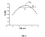
図7は、ウエハ表面12上における位置の関数としてのウエハ表面温度TS(K)のグラフであり、非溶融レーザービーム168による走査方向に沿った、典型的なウエハ表面温度プロファイルを示している。非溶融加熱による実質的に均一な部分は「u」で示されており、また、同部分は、予め規定された非均一性の許容値εよりも温度ロールオフが小さい最大表面温度TSMの近傍領域である。一例として、ε=10℃の場合において、uの値は、概略、非溶融レーザービーム幅W1の20%以下である。
FIG. 7 is a graph of wafer surface temperature T S (K) as a function of position on
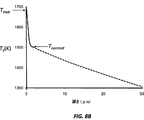
図8Aは、ウエハ表面温度TS(K)と時間(ms)との関係を示すグラフであり、図8Bは、温度TS(K)と深さとの関係を示すグラフである。図8Aにおいて、温度プロファイルの非溶融部分は、非溶融最大温度Tnonmeltでピークとなる破線で示されている。図8Bにおいて、溶融部分は点線で示されており、非溶融部分は実線で示されている。 FIG. 8A is a graph showing the relationship between wafer surface temperature T S (K) and time (ms), and FIG. 8B is a graph showing the relationship between temperature T S (K) and depth. In FIG. 8A, the non-melting portion of the temperature profile is indicated by a broken line that peaks at the non-melting maximum temperature T nonmelt . In FIG. 8B, the melted part is indicated by a dotted line, and the non-melted part is indicated by a solid line.
図8Aおよび図8Bの2つのグラフは、本発明にかかる超高速レーザーアニーリング方法の一例が適用されるウエハ表面12上の一点における、シミュレーションによる、時間および深さに関するウエハ表面温度プロファイルを示している。実施例において、非溶融レーザー160は、滞留時間tDが0.8msのCO2レーザーである。非溶融ラインイメージ170でウエハ表面12を走査することによって生じた最大ウエハ表面温度TSMは、1500K(1227℃)であった。溶融レーザー260は、パルス持続時間ΔtMが30nsの溶融光パルス268Pを生成する。当該溶融レーザービーム268は、流束量が75mJ/cm2であり、波長が532nmである。図8Aの差込図は、溶融レーザービーム268に関する、より詳細な溶融温度プロファイルを示す。この温度プロファイルは、グラフ全体において、ピークが約1685K(すなわち、約1412℃)の温度突出部として示されている。
The two graphs of FIGS. 8A and 8B show simulated wafer surface temperature profiles with respect to time and depth at a point on the
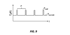
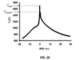
図9は、時間t(任意の単位)の関数としてのウエハ表面温度TS(K)の例を示すグラフであり、図6Aに示されるような超高速レーザーアニーリング方法の一例における、理想的なウエハ表面温度プロファイルを示している。図10は、ウエハ表面温度TS(K)と時間(ms)との関係を示すグラフであり、2本の非溶融レーザービーム構成を用いた場合における、ウエハ表面12におけるアニーリング温度TSの時間発展を示している。ウエハ10の非溶融プレヒート温度は、パイロメータ280を用いてウエハ表面12上の被加熱スポットからの熱放射を監視するとともに、温度信号STをシステムコントローラ300にフィードバックすることによって一定に維持される。溶融加熱による熱放射が非溶融レーザービーム168の制御を妨げないように、溶融光パルス268Pに起因する複数のTmeltピーク(図9を参照)同士の間で非溶融フィードバック制御のためのデータサンプリングを実施する。Tmeltピーク(図9を参照)同士の間の期間Pは、溶融光パルス268Pの繰返し率の逆数で表すことができる。
FIG. 9 is a graph showing an example of wafer surface temperature T S (K) as a function of time t (arbitrary units), which is ideal for an example of an ultrafast laser annealing method as shown in FIG. 6A. 3 shows a wafer surface temperature profile. FIG. 10 is a graph showing the relationship between the wafer surface temperature T S (K) and time (ms), and the time of the annealing temperature T S on the
向上した表面温度均一性
本発明にかかる超高速レーザーアニーリングシステムおよび方法の利点は、前述したパターン密度効果の不利益を軽減することによってウエハ表面12の温度均一性を向上させる点にある。第1に、レーザーアニーリング処理の実施に関係する温度変動(すなわち、非均一性)ΔTは、下記の数式によって見積もることができる。
通常、熱拡散長さの桁が違うこと、さらに、入射角θ1のブルースター角で運用するCO2レーザー(例えば、10.6ミクロン)のような長波長非溶融レーザー160を使用することにより、ΔTnonmeltはΔTmeltよりも十分に小さい。前者は、不均一な熱特性によるパターン密度効果を低減する一方で、後者は、光学的吸収の非均一性によるパターン密度効果を低減する。結果として、ΔTに関する上記の式は、下記のようになる。
非溶融温度Tnonmeltが溶融温度Tmeltの近くまで上昇すると、すべてのパターン密度効果は、著しく減少することになる。実際、最大非溶融温度Tnonmeltは、スリップ発生や酸化膜欠陥といった特定の半導体プロセスによって制限される。シリコン基板10の場合、Tmeltは1412℃であり、Tnonmeltは1000から1350℃の範囲にある。このため、Tsubを400℃と推定すると、下記の通りになる。
上記数式を使用することにより、特定の半導体プロセスにおける許容温度変化量(不均一性)ΔTを得るために必要とする最小非溶融温度Tnonmeltを計算することができる。例えば、仮に要求される温度均一性が20℃以下(すなわち、ΔT<20℃)であり、ΔTmelt=100℃、Tsub=400℃、Tmelt=1412℃の場合は下記の通りになる。
Tnonmeltを解くためには、下記の通りになる。
これは、非均一性の幅が目標の20℃を達成するのに必要な最小非溶融温度Tnonmeltが1210℃であることを意味している。非溶融温度Tnonmeltが高いほど、全体の温度非均一性ΔTは小さくなる。 This means that the minimum non-melting temperature T nonmelt necessary to achieve the target non-uniformity range of 20 ° C. is 1210 ° C. The higher the non-melting temperature T nonmelt, the smaller the overall temperature non-uniformity ΔT.
図11は、図2と同様の図であり、本発明にかかるレーザーアニーリングシステムおよび方法が、従来の溶融レーザーアニーリング手法(図2)と比較して、どのようにして、2つのゲートG1およびG2の温度差を低減させてパターン密度効果を軽減し得るかを示している。 FIG. 11 is a view similar to FIG. 2 and shows how the laser annealing system and method according to the present invention compares the two gates G1 and G2 as compared to the conventional melt laser annealing technique (FIG. 2). It is shown whether the temperature density difference can be reduced to reduce the pattern density effect.
非溶融レーザープレヒートに非溶融レーザービーム168を用いることにより、溶融レーザー260に求められる流束量は、従来の溶融レーザーアニーリングに比べて、著しく低められる。例えば、非溶融レーザービーム168によって1500Kまで非溶融プレヒートされる場合、溶融レーザー260および関連する溶融レーザービーム268に要求される流束量は、従来の溶融レーザーアニーリングプロセスに求められる流束量の約17%である。
By using the
本発明にかかるレーザーアニーリングシステムおよび方法は、さらに、従来の溶融レーザーアニーリングシステムおよび方法に比べて、レーザーアニーリングプロセスウィンドウを向上させることもできる。図12は、溶融深さ(nm)と、30nmの非結晶化接合を有するシリコンウエハに対する規格化したレーザー流束量との関係を示しており、関連プロセスウィンドウPW1を有する従来の溶融レーザーアニーリング(実線)と、関連プロセスウィンドウPW2を有する本発明にかかる超高速レーザーアニーリング(破線)とが示されている。 The laser annealing system and method according to the present invention can also improve the laser annealing process window as compared to conventional melt laser annealing systems and methods. FIG. 12 shows the relationship between the melt depth (nm) and the normalized laser flux for a silicon wafer with a 30 nm non-crystallized junction, with conventional melt laser annealing with an associated process window PW1 ( Solid line) and ultrafast laser annealing (dashed line) according to the invention with an associated process window PW2 are shown.
非結晶化は、ウエハ10のより低い溶融温度によってもたらされる。これにより、接合部温度が非結晶シリコンよりも高く結晶シリコンよりも低い場合、溶融深さが所定の範囲の流束量(プロセスウィンドウとして定義される)に収まる。プロセスウィンドウPW2の劇的な改善は、従来の溶融レーザーアニーリング(実線および実線矢印)のプロセスウィンドウPW1と比べて、1300KのTnonmelt(破線および破線矢印)において見られる。Tnonmeltおよび非溶融滞留時間は、溶融温度Tmeltに達する前に非結晶シリコンを完全に結晶化させないように最適化すべきである。
Non-crystallization is caused by the lower melting temperature of the
本発明にかかるレーザーアニーリングシステムおよび方法の他の利点として、従来の溶融レーザーアニーリングシステムおよび方法と比較して、欠陥の治癒の向上、および精密なドーパント拡散の最適化が挙げられる。従来の溶融レーザーアニーリングプロセスでは、熱量が極めて小さいことにより、溶融領域外に埋め込まれたダメージを回復させることができない。このため、高い接合部漏れ電流の原因となり得る。一方、本発明の超高速レーザーアニーリングシステムおよび方法によれば、より大きな熱量が適用されるとともに、長い非溶融対流時間tD(例えば、数ミリ秒から数十ミリ秒)における接合部漏れ電流が向上することが実証されている。最適なトランジスタ性能のため、例えわずかであってもドーパントプロファイルを最適化するフレキシブルさを有することが望ましい。従来の溶融レーザーアニーリングでこれを達成するのは難しいが、本発明にかかるレーザーアニーリングシステムおよび方法を用いて、非溶融滞留時間および非溶融プレヒート温度の少なくとも一方を変化させることにより、これを達成することができる。 Other advantages of the laser annealing system and method according to the present invention include improved defect healing and optimization of precise dopant diffusion compared to conventional melt laser annealing systems and methods. In the conventional melting laser annealing process, the damage embedded outside the melting region cannot be recovered due to the extremely small amount of heat. This can cause high junction leakage current. On the other hand, according to the ultrafast laser annealing system and method of the present invention, a larger amount of heat is applied, and the junction leakage current at a long non-melting convection time t D (eg, several milliseconds to several tens of milliseconds) It has been proven to improve. For optimum transistor performance, it is desirable to have the flexibility to optimize the dopant profile, even if only slightly. While this is difficult to achieve with conventional melt laser annealing, this is accomplished using the laser annealing system and method according to the present invention by varying at least one of the non-melt residence time and the non-melt preheat temperature. be able to.
図13は、図1と同様、システム100の一部の概略側面図であり、ガス浸漬レーザードーピングを伴う超高速レーザーアニーリングを実施するシステム100の実施例を示している。図13において、ウエハ10は、チャンバー400のチャンバー内部401に収容されている。チャンバー400は、非溶融レーザービーム168および溶融レーザービーム268に用いられる波長の光を実質的に透過するウィンドウ408を有する天面402を備えている。システム100は、ガスライン430を通じてガス状のドーパントプレカーサ424をチャンバー内部401およびウエハ表面12の近傍に供給するガス源420を備えている。チャンバー内部401は、ウエハ表面12の近傍にガス状のドーパントプレカーサ424を使用可能に導くようになっている。
FIG. 13 is a schematic side view of a portion of the
一例において、システムコントローラ300は、ガス源420に使用可能に接続されており、上記の他のレーザーアニーリングと連携して制御を行う。本実施例において、チャンバー内のレーザーエネルギーは、ウエハ表面12を加熱するのと同じく、ガス状のドーパントプレカーサ424を解離させる。これにより、レーザーアニーリングプロセス中にガス状のドーパントプレカーサ424からのドーパントをウエハ表面12に拡散注入させることができる。ガス状のドーパントプレカーサ424の例として、Asドーピング用のAsH3、およびBドーピング用のBF3、BCl3、B(CH3)3を挙げることができる。
In one example, the
ガス浸漬レーザーアニーリングの適用に関して、ガス状のドーパントプレカーサ424の効果的な解離のための高光子エネルギーを提供するために、波長308nmのXeClエキシマレーザーや波長355nmの周波数3倍YAGレーザーといった短波長溶融レーザー260が望ましい。ガス浸漬レーザードーピングシステムおよび方法の例として、米国特許番号5,908,307、5,888,888、5,849,043、および5,316,969が挙げられ、これら全ては、本明細書に援用される。
For application of gas immersion laser annealing, short wavelength melting such as XeCl excimer laser with a wavelength of 308 nm or frequency tripled YAG laser with a wavelength of 355 nm to provide high photon energy for effective dissociation of the
当業者には明白であるが、本発明の精神および範囲を逸脱することなく、本発明に対して様々な修正及び変更を加えることができる。したがって、本発明は、添付の特許請求の範囲およびその均等範囲内において本発明の修正及び変更を包含する。 It will be apparent to those skilled in the art that various modifications and variations can be made to the present invention without departing from the spirit and scope of the invention. Accordingly, the present invention includes modifications and variations of this invention within the scope of the appended claims and their equivalents.
図8Aは、ウエハ表面温度TS(K)と時間(ms)との関係を示すグラフであり、図8Bは、温度TS(K)と深さとの関係を示すグラフである。図8Aにおいて、温度プロファイルの非溶融部分は、非溶融最大温度Tnonmeltでピークとなる破線で示されている。図8Bにおいて、溶融部分は実線で示されており、非溶融部分は破線で示されている。 FIG. 8A is a graph showing the relationship between wafer surface temperature T S (K) and time (ms), and FIG. 8B is a graph showing the relationship between temperature T S (K) and depth. In FIG. 8A, the non-melting portion of the temperature profile is indicated by a broken line that peaks at the non-melting maximum temperature T nonmelt . In FIG. 8B, the melted portion is indicated by a solid line , and the non-melted portion is indicated by a broken line .
Claims (34)
前記溶融温度から400℃以内にある非溶融温度Tnonmeltまで前記パターン付き表面を加熱する少なくとも一つの第1レーザービームで前記パターン付き表面を走査し、
パルス状であり、かつ、前記非溶融温度から前記溶融温度まで前記パターン付き表面を加熱する、前記第1レーザービームと関連する少なくとも一つの第2レーザービームで前記パターン付き表面を走査する方法。 A method for annealing a semiconductor substrate having a patterned surface and a melting temperature comprising:
Scanning the patterned surface with at least one first laser beam that heats the patterned surface to a non-melting temperature T nonmelt within 400 ° C. from the melting temperature;
A method of scanning the patterned surface with at least one second laser beam associated with the first laser beam, wherein the patterned surface is pulsed and heats the patterned surface from the non-melting temperature to the melting temperature.
前記少なくとも一つの第2レーザービームは、前記パターン付き表面において少なくとも一つの溶融ラインイメージを形成し、
前記パターン付き表面において、前記少なくとも一つの溶融ラインイメージは、前記少なくとも一つの非溶融ラインイメージと部分的に重なり合っている、請求項1または2に記載の方法。 The at least one first laser beam forms at least one non-melting line image on the patterned surface;
The at least one second laser beam forms at least one melt line image on the patterned surface;
The method of claim 1 or 2, wherein at the patterned surface, the at least one melt line image partially overlaps the at least one non-melt line image.
前記少なくとも一つの非溶融ラインイメージおよび前記少なくとも一つの溶融ラインイメージによる走査は、前記少なくとも一つの溶融ラインイメージが実質的に前記少なくとも一つの非溶融ラインイメージの前記ピーク温度軸に沿って形成されるようにして実行される、請求項3に記載の方法。 The at least one non-melting line image is associated with a peak temperature axis corresponding to a maximum non-melting temperature of the patterned surface by scanning the patterned surface with the at least one first laser beam;
The at least one non-melt line image and the at least one melt line image scan are formed such that the at least one melt line image is substantially along the peak temperature axis of the at least one non-melt line image. 4. The method according to claim 3, wherein the method is performed as described above.
前記溶融温度から約400℃内にある非溶融温度Tnonmeltまで前記パターン付き表面を加熱する少なくとも一つの第1レーザービームを生成するとともに、前記少なくとも一つの第1レーザービームで前記パターン付き表面を走査する第1レーザーシステムと、
パルス状で、かつ、前記非溶融温度から前記溶融温度まで前記パターン付き表面を加熱する少なくとも一つの第2レーザービームを生成するとともに、前記第1レーザービームに関連して前記少なくとも一つの第2レーザービームで前記パターン付き表面を走査する第2レーザーシステムとを備えるシステム。 A system used for laser annealing of a semiconductor substrate having a patterned surface and a melting temperature,
Generating at least one first laser beam for heating the patterned surface from the melting temperature to a non-melting temperature T nonmelt within about 400 ° C. and scanning the patterned surface with the at least one first laser beam; A first laser system to
Generating at least one second laser beam that is pulsed and that heats the patterned surface from the non-melting temperature to the melting temperature, and wherein the at least one second laser is associated with the first laser beam; A second laser system for scanning the patterned surface with a beam.
前記第2レーザービームは、前記パターン付き表面における少なくとも一つの溶融ラインイメージを形成し、
前記第1レーザーシステムおよび前記第2レーザーシステムは、前記少なくとも一つの溶融ラインイメージおよび前記少なくとも一つの非溶融ラインイメージを前記パターン付き表面において少なくとも部分的に重複させる、請求項16に記載のシステム。 The at least one first laser beam forms at least one non-melting line image on the patterned surface;
The second laser beam forms at least one melt line image on the patterned surface;
The system of claim 16, wherein the first laser system and the second laser system at least partially overlap the at least one melt line image and the at least one non-melt line image at the patterned surface.
前記第1レーザーシステムおよび前記第2レーザーシステムは、前記少なくとも一つの溶融ラインイメージが、実質的に前記少なくとも一つの非溶融ラインイメージの前記ピーク温度軸に沿って形成されるように構成されている、請求項17に記載のシステム。 The at least one non-melting line image is associated with a peak temperature axis corresponding to a maximum non-melting of the patterned surface resulting from scanning the patterned surface with the at least one first laser beam; and
The first laser system and the second laser system are configured such that the at least one melt line image is formed substantially along the peak temperature axis of the at least one non-melt line image. The system of claim 17.
前記パターン付き表面における温度ムラΔTを選択し、
下記の関係から最低非溶融温度Tnonmeltを決定し、
少なくとも一つの第1レーザービームで走査して前記パターン付き表面を前記最小非溶融温度Tnonmeltから前記溶融温度よりも約50℃低い温度の範囲の非溶融温度まで加熱し、前記第1レーザービームに関連する少なくとも一つの第2パルス状レーザービームで走査して前記基板溶融温度Tmeltまで前記パターン付き表面を加熱するレーザーアニーリングを実施する方法。 A method for laser annealing a substrate having a patterned surface and a predetermined melting temperature T melt comprising:
Select temperature irregularity ΔT on the patterned surface,
The minimum non-melting temperature T nonmelt is determined from the following relationship,
The patterned surface is scanned with at least one first laser beam to heat the patterned surface from the minimum non-melting temperature T nonmelt to a non-melting temperature in the range of about 50 ° C. below the melting temperature. Performing laser annealing by scanning with at least one associated second pulsed laser beam to heat the patterned surface to the substrate melting temperature T melt .
前記少なくとも一つの非溶融ラインイメージおよび前記少なくとも一つの溶融ラインイメージの一方が前記パターン付き表面における領域の寸法に対応した長さを有している、請求項22から30のいずれかに記載の方法。 On the patterned surface, at least one non-melting line image is formed with the at least one first laser beam, and at least one melting line image is formed with the at least one second laser beam;
31. A method according to any one of claims 22 to 30, wherein one of the at least one non-melt line image and the at least one melt line image has a length corresponding to the size of a region in the patterned surface. .
34. The patterned surface of claim 22 to 33, wherein the patterned surface has a dopant profile that is adjusted by adjusting at least one of the at least one first laser beam and the at least one second laser beam. The method according to any one.
Applications Claiming Priority (2)
| Application Number | Priority Date | Filing Date | Title |
|---|---|---|---|
| US13/134,408 US8309474B1 (en) | 2011-06-07 | 2011-06-07 | Ultrafast laser annealing with reduced pattern density effects in integrated circuit fabrication |
| US13/134,408 | 2011-06-07 |
Publications (2)
| Publication Number | Publication Date |
|---|---|
| JP2012256879A true JP2012256879A (en) | 2012-12-27 |
| JP5602787B2 JP5602787B2 (en) | 2014-10-08 |
Family
ID=47114488
Family Applications (1)
| Application Number | Title | Priority Date | Filing Date |
|---|---|---|---|
| JP2012112240A Expired - Fee Related JP5602787B2 (en) | 2011-06-07 | 2012-05-16 | Ultrafast laser annealing with reduced pattern density effects in integrated circuit manufacturing |
Country Status (5)
| Country | Link |
|---|---|
| US (1) | US8309474B1 (en) |
| JP (1) | JP5602787B2 (en) |
| KR (1) | KR20120135867A (en) |
| SG (1) | SG186542A1 (en) |
| TW (1) | TWI497600B (en) |
Cited By (5)
| Publication number | Priority date | Publication date | Assignee | Title |
|---|---|---|---|---|
| JP2016105470A (en) * | 2014-11-24 | 2016-06-09 | ウルトラテック インク | High-performance line-forming optical system and method for defect annealing and dopant activation |
| KR20180098383A (en) * | 2015-12-30 | 2018-09-03 | 상하이 마이크로 일렉트로닉스 이큅먼트(그룹) 컴퍼니 리미티드 | Laser annealing apparatus and annealing method thereof |
| JP2019125748A (en) * | 2018-01-18 | 2019-07-25 | トヨタ自動車株式会社 | Manufacturing method of semiconductor device |
| JP2019125761A (en) * | 2018-01-19 | 2019-07-25 | 富士電機株式会社 | Impurity introduction device, impurity introduction method, and method for manufacturing silicon carbide semiconductor device |
| JP2019125762A (en) * | 2018-01-19 | 2019-07-25 | 富士電機株式会社 | Impurity introduction method and method for manufacturing semiconductor device |
Families Citing this family (15)
| Publication number | Priority date | Publication date | Assignee | Title |
|---|---|---|---|---|
| US8546805B2 (en) * | 2012-01-27 | 2013-10-01 | Ultratech, Inc. | Two-beam laser annealing with improved temperature performance |
| US9490128B2 (en) * | 2012-08-27 | 2016-11-08 | Ultratech, Inc. | Non-melt thin-wafer laser thermal annealing methods |
| WO2015023791A1 (en) | 2013-08-16 | 2015-02-19 | Applied Materials, Inc. | Dynamic optical valve for mitigating non-uniform heating in laser processing |
| US9559023B2 (en) | 2014-06-23 | 2017-01-31 | Ultratech, Inc. | Systems and methods for reducing beam instability in laser annealing |
| US9613828B2 (en) | 2014-06-24 | 2017-04-04 | Ultratech, Inc. | Method of laser annealing a semiconductor wafer with localized control of ambient oxygen |
| CN106663629B (en) * | 2014-07-21 | 2020-01-10 | 应用材料公司 | Scanning pulse annealing device and method |
| WO2016068741A1 (en) * | 2014-10-28 | 2016-05-06 | Общество С Ограниченной Ответственностью "Солэкс-С" | Laser doping method and device for carrying out same |
| US10083843B2 (en) | 2014-12-17 | 2018-09-25 | Ultratech, Inc. | Laser annealing systems and methods with ultra-short dwell times |
| US10247952B2 (en) * | 2015-03-04 | 2019-04-02 | Coherent Lasersystems Gmbh & Co. Kg | Polarization-controlled laser line-projector |
| US9859121B2 (en) * | 2015-06-29 | 2018-01-02 | International Business Machines Corporation | Multiple nanosecond laser pulse anneal processes and resultant semiconductor structure |
| KR102013670B1 (en) * | 2017-05-18 | 2019-08-26 | 세메스 주식회사 | Substrate treating apparatus and substrate treating method |
| KR101962859B1 (en) * | 2017-05-18 | 2019-03-28 | 세메스 주식회사 | Substrate treating apparatus and substrate treating method |
| US11352698B2 (en) | 2019-04-25 | 2022-06-07 | Samsung Electronics Co., Ltd. | Atomic layer deposition apparatus and methods of fabricating semiconductor devices using the same |
| US11909091B2 (en) | 2020-05-19 | 2024-02-20 | Kymeta Corporation | Expansion compensation structure for an antenna |
| EP3970898A1 (en) | 2020-09-18 | 2022-03-23 | Laser Systems & Solutions of Europe | System and method to minimize irradiation non uniformity |
Citations (10)
| Publication number | Priority date | Publication date | Assignee | Title |
|---|---|---|---|---|
| JPH0521340A (en) * | 1991-07-10 | 1993-01-29 | Ricoh Co Ltd | Thin film semiconductor device, method and apparatus for manufacturing the same |
| JPH0974067A (en) * | 1995-09-05 | 1997-03-18 | Mitsubishi Electric Corp | Doping method and doping device |
| JP2000133613A (en) * | 1999-11-15 | 2000-05-12 | Seiko Epson Corp | Manufacture of semiconductor thin film |
| JP2000216088A (en) * | 1999-01-20 | 2000-08-04 | Sony Corp | Method of forming semiconductor thin film and laser irradiator |
| JP2004006725A (en) * | 2002-03-26 | 2004-01-08 | Semiconductor Energy Lab Co Ltd | Semiconductor device, its fabricating and designing method |
| JP2004515085A (en) * | 2000-12-04 | 2004-05-20 | ボルテック インダストリーズ リミテッド | Heat treatment method and system |
| JP2004266102A (en) * | 2003-02-28 | 2004-09-24 | Semiconductor Energy Lab Co Ltd | Device and method of laser irradiation, and method for manufacturing semiconductor device |
| JP2004281771A (en) * | 2003-03-17 | 2004-10-07 | Sharp Corp | Crystal growth method and crystal growth device for semiconductor thin film and manufacturing method for thin film transistor |
| JP2008047923A (en) * | 2006-08-17 | 2008-02-28 | Toshiba Corp | Laser spike annealing employing a plurality of light sources |
| JP2010109363A (en) * | 2008-10-06 | 2010-05-13 | Ultratech Inc | Thermal processing of substrate with pre- and post-spike temperature control |
Family Cites Families (43)
| Publication number | Priority date | Publication date | Assignee | Title |
|---|---|---|---|---|
| US4234356A (en) | 1979-06-01 | 1980-11-18 | Bell Telephone Laboratories, Incorporated | Dual wavelength optical annealing of materials |
| JPS56142630A (en) | 1980-04-09 | 1981-11-07 | Fujitsu Ltd | Manufacture of semiconductor device |
| JP3211377B2 (en) | 1992-06-17 | 2001-09-25 | ソニー株式会社 | Method for manufacturing semiconductor device |
| KR100255689B1 (en) | 1993-05-27 | 2000-05-01 | 윤종용 | Semiconductor laser device and its manufacturing method |
| KR100274293B1 (en) | 1995-06-26 | 2001-01-15 | 야스카와 히데아키 | Crystalline semiconductor film forming method, thin film transistor manufacturing method, solar cell manufacturing method and active matrix liquid crystal device |
| US6524977B1 (en) | 1995-07-25 | 2003-02-25 | Semiconductor Energy Laboratory Co., Ltd. | Method of laser annealing using linear beam having quasi-trapezoidal energy profile for increased depth of focus |
| JP3348334B2 (en) | 1995-09-19 | 2002-11-20 | ソニー株式会社 | Method for manufacturing thin film semiconductor device |
| KR0153823B1 (en) | 1995-10-17 | 1998-12-01 | 구자홍 | Method of manufacturing semiconductor device |
| JP3301054B2 (en) | 1996-02-13 | 2002-07-15 | 株式会社半導体エネルギー研究所 | Laser irradiation device and laser irradiation method |
| JPH1174536A (en) | 1997-01-09 | 1999-03-16 | Sanyo Electric Co Ltd | Manufacture of semiconductor device |
| US5908307A (en) | 1997-01-31 | 1999-06-01 | Ultratech Stepper, Inc. | Fabrication method for reduced-dimension FET devices |
| JPH10244392A (en) | 1997-03-04 | 1998-09-14 | Semiconductor Energy Lab Co Ltd | Laser irradiation device |
| TW466772B (en) | 1997-12-26 | 2001-12-01 | Seiko Epson Corp | Method for producing silicon oxide film, method for making semiconductor device, semiconductor device, display, and infrared irradiating device |
| US5930617A (en) | 1998-03-25 | 1999-07-27 | Texas Instruments-Acer Incorporated | Method of forming deep sub-micron CMOS transistors with self-aligned silicided contact and extended S/D junction |
| KR100430231B1 (en) | 1998-10-02 | 2004-07-19 | 엘지.필립스 엘시디 주식회사 | Laser Annealing Equipment |
| US6521501B1 (en) | 1999-05-11 | 2003-02-18 | Advanced Micro Devices, Inc. | Method of forming a CMOS transistor having ultra shallow source and drain regions |
| TW473783B (en) | 1999-08-13 | 2002-01-21 | Semiconductor Energy Lab | Laser apparatus, laser annealing method, and manufacturing method of a semiconductor device |
| US6514339B1 (en) | 1999-10-29 | 2003-02-04 | Lg. Philips Co., Ltd. | Laser annealing apparatus |
| JP4514861B2 (en) | 1999-11-29 | 2010-07-28 | 株式会社半導体エネルギー研究所 | Laser irradiation apparatus, laser irradiation method, and manufacturing method of semiconductor device |
| US6366308B1 (en) | 2000-02-16 | 2002-04-02 | Ultratech Stepper, Inc. | Laser thermal processing apparatus and method |
| US6531681B1 (en) | 2000-03-27 | 2003-03-11 | Ultratech Stepper, Inc. | Apparatus having line source of radiant energy for exposing a substrate |
| US6303476B1 (en) | 2000-06-12 | 2001-10-16 | Ultratech Stepper, Inc. | Thermally induced reflectivity switch for laser thermal processing |
| US6368947B1 (en) | 2000-06-20 | 2002-04-09 | Advanced Micro Devices, Inc. | Process utilizing a cap layer optimized to reduce gate line over-melt |
| US6479821B1 (en) | 2000-09-11 | 2002-11-12 | Ultratech Stepper, Inc. | Thermally induced phase switch for laser thermal processing |
| US6365476B1 (en) | 2000-10-27 | 2002-04-02 | Ultratech Stepper, Inc. | Laser thermal process for fabricating field-effect transistors |
| US7015422B2 (en) * | 2000-12-21 | 2006-03-21 | Mattson Technology, Inc. | System and process for heating semiconductor wafers by optimizing absorption of electromagnetic energy |
| KR20040052468A (en) | 2001-11-12 | 2004-06-23 | 소니 가부시끼 가이샤 | Laser annealing device and thin-film transistor manufacturing method |
| US6849831B2 (en) * | 2002-03-29 | 2005-02-01 | Mattson Technology, Inc. | Pulsed processing semiconductor heating methods using combinations of heating sources |
| US6987240B2 (en) | 2002-04-18 | 2006-01-17 | Applied Materials, Inc. | Thermal flux processing by scanning |
| US7005601B2 (en) | 2002-04-18 | 2006-02-28 | Applied Materials, Inc. | Thermal flux processing by scanning |
| US6548361B1 (en) | 2002-05-15 | 2003-04-15 | Advanced Micro Devices, Inc. | SOI MOSFET and method of fabrication |
| US6747245B2 (en) | 2002-11-06 | 2004-06-08 | Ultratech Stepper, Inc. | Laser scanning apparatus and methods for thermal processing |
| US7304005B2 (en) | 2003-03-17 | 2007-12-04 | Semiconductor Energy Laboratory Co., Ltd. | Laser irradiation apparatus, laser irradiation method, and method for manufacturing a semiconductor device |
| JP4373115B2 (en) | 2003-04-04 | 2009-11-25 | 株式会社半導体エネルギー研究所 | Method for manufacturing semiconductor device |
| US7098155B2 (en) | 2003-09-29 | 2006-08-29 | Ultratech, Inc. | Laser thermal annealing of lightly doped silicon substrates |
| US7772523B2 (en) | 2004-07-30 | 2010-08-10 | Semiconductor Energy Laboratory Co., Ltd | Laser irradiation apparatus and laser irradiation method |
| US7279721B2 (en) | 2005-04-13 | 2007-10-09 | Applied Materials, Inc. | Dual wavelength thermal flux laser anneal |
| US7482254B2 (en) | 2005-09-26 | 2009-01-27 | Ultratech, Inc. | Apparatus and methods for thermally processing undoped and lightly doped substrates without pre-heating |
| US7514305B1 (en) * | 2006-06-28 | 2009-04-07 | Ultratech, Inc. | Apparatus and methods for improving the intensity profile of a beam image used to process a substrate |
| US7691755B2 (en) * | 2007-05-15 | 2010-04-06 | Applied Materials, Inc. | Plasma immersion ion implantation with highly uniform chamber seasoning process for a toroidal source reactor |
| US20090034071A1 (en) | 2007-07-31 | 2009-02-05 | Dean Jennings | Method for partitioning and incoherently summing a coherent beam |
| US7709370B2 (en) * | 2007-09-20 | 2010-05-04 | International Business Machines Corporation | Spin-on antireflective coating for integration of patternable dielectric materials and interconnect structures |
| US8026519B1 (en) | 2010-10-22 | 2011-09-27 | Ultratech, Inc. | Systems and methods for forming a time-averaged line image |
-
2011
- 2011-06-07 US US13/134,408 patent/US8309474B1/en not_active Expired - Fee Related
-
2012
- 2012-05-08 SG SG2012033775A patent/SG186542A1/en unknown
- 2012-05-16 JP JP2012112240A patent/JP5602787B2/en not_active Expired - Fee Related
- 2012-05-24 KR KR1020120055387A patent/KR20120135867A/en not_active Application Discontinuation
- 2012-06-06 TW TW101120334A patent/TWI497600B/en not_active IP Right Cessation
Patent Citations (10)
| Publication number | Priority date | Publication date | Assignee | Title |
|---|---|---|---|---|
| JPH0521340A (en) * | 1991-07-10 | 1993-01-29 | Ricoh Co Ltd | Thin film semiconductor device, method and apparatus for manufacturing the same |
| JPH0974067A (en) * | 1995-09-05 | 1997-03-18 | Mitsubishi Electric Corp | Doping method and doping device |
| JP2000216088A (en) * | 1999-01-20 | 2000-08-04 | Sony Corp | Method of forming semiconductor thin film and laser irradiator |
| JP2000133613A (en) * | 1999-11-15 | 2000-05-12 | Seiko Epson Corp | Manufacture of semiconductor thin film |
| JP2004515085A (en) * | 2000-12-04 | 2004-05-20 | ボルテック インダストリーズ リミテッド | Heat treatment method and system |
| JP2004006725A (en) * | 2002-03-26 | 2004-01-08 | Semiconductor Energy Lab Co Ltd | Semiconductor device, its fabricating and designing method |
| JP2004266102A (en) * | 2003-02-28 | 2004-09-24 | Semiconductor Energy Lab Co Ltd | Device and method of laser irradiation, and method for manufacturing semiconductor device |
| JP2004281771A (en) * | 2003-03-17 | 2004-10-07 | Sharp Corp | Crystal growth method and crystal growth device for semiconductor thin film and manufacturing method for thin film transistor |
| JP2008047923A (en) * | 2006-08-17 | 2008-02-28 | Toshiba Corp | Laser spike annealing employing a plurality of light sources |
| JP2010109363A (en) * | 2008-10-06 | 2010-05-13 | Ultratech Inc | Thermal processing of substrate with pre- and post-spike temperature control |
Cited By (9)
| Publication number | Priority date | Publication date | Assignee | Title |
|---|---|---|---|---|
| JP2016105470A (en) * | 2014-11-24 | 2016-06-09 | ウルトラテック インク | High-performance line-forming optical system and method for defect annealing and dopant activation |
| KR20180098383A (en) * | 2015-12-30 | 2018-09-03 | 상하이 마이크로 일렉트로닉스 이큅먼트(그룹) 컴퍼니 리미티드 | Laser annealing apparatus and annealing method thereof |
| JP2019507493A (en) * | 2015-12-30 | 2019-03-14 | シャンハイ マイクロ エレクトロニクス イクイプメント(グループ)カンパニー リミティド | Laser annealing apparatus and laser annealing method therefor |
| KR102080613B1 (en) | 2015-12-30 | 2020-02-24 | 상하이 마이크로 일렉트로닉스 이큅먼트(그룹) 컴퍼니 리미티드 | Laser annealing device and its annealing method |
| JP2019125748A (en) * | 2018-01-18 | 2019-07-25 | トヨタ自動車株式会社 | Manufacturing method of semiconductor device |
| JP7087401B2 (en) | 2018-01-18 | 2022-06-21 | 株式会社デンソー | Manufacturing method of semiconductor device |
| JP2019125761A (en) * | 2018-01-19 | 2019-07-25 | 富士電機株式会社 | Impurity introduction device, impurity introduction method, and method for manufacturing silicon carbide semiconductor device |
| JP2019125762A (en) * | 2018-01-19 | 2019-07-25 | 富士電機株式会社 | Impurity introduction method and method for manufacturing semiconductor device |
| JP7024433B2 (en) | 2018-01-19 | 2022-02-24 | 富士電機株式会社 | Impurity introduction device, impurity introduction method and silicon carbide semiconductor device manufacturing method |
Also Published As
| Publication number | Publication date |
|---|---|
| SG186542A1 (en) | 2013-01-30 |
| TW201250854A (en) | 2012-12-16 |
| JP5602787B2 (en) | 2014-10-08 |
| TWI497600B (en) | 2015-08-21 |
| US8309474B1 (en) | 2012-11-13 |
| KR20120135867A (en) | 2012-12-17 |
Similar Documents
| Publication | Publication Date | Title |
|---|---|---|
| JP5602787B2 (en) | Ultrafast laser annealing with reduced pattern density effects in integrated circuit manufacturing | |
| US9302348B2 (en) | Ultrafast laser annealing with reduced pattern density effects in integrated circuit fabrication | |
| JP5105984B2 (en) | Beam irradiation apparatus and laser annealing method | |
| US10847381B2 (en) | Laser annealing systems and methods with ultra-short dwell times | |
| JP5517396B2 (en) | Laser thermal annealing of lightly doped silicon substrates | |
| JP4117020B2 (en) | Semiconductor device manufacturing method and semiconductor device manufacturing apparatus | |
| TWI549191B (en) | Managing thermal budget in annealing of substrates | |
| JP6910742B2 (en) | Laser annealing method and laser annealing equipment | |
| US20150017817A1 (en) | Laser processing apparatus and laser processing method | |
| JP5246716B2 (en) | Semiconductor substrate manufacturing method and laser annealing apparatus | |
| JP2012044046A (en) | Apparatus and method for laser annealing | |
| EP2943973B1 (en) | Thermal processing by transmission of mid infra-red laser light through semiconductor substrate | |
| JP5660880B2 (en) | Laser annealing method | |
| JP2015115401A (en) | Laser annealing method and laser anneal device | |
| JP2017028017A (en) | Laser anneal device and laser anneal method | |
| JP2014195004A (en) | Process of manufacturing semiconductor element and manufacturing apparatus of semiconductor element | |
| JP2009078947A (en) | Light irradiation method and light irradiation apparatus | |
| JP2008306210A (en) | Method of manufacturing semiconductor device | |
| JP2008306211A (en) | Manufacturing method of semiconductor device, and laser annealing device |
Legal Events
| Date | Code | Title | Description |
|---|---|---|---|
| A621 | Written request for application examination |
Free format text: JAPANESE INTERMEDIATE CODE: A621 Effective date: 20130513 |
|
| A977 | Report on retrieval |
Free format text: JAPANESE INTERMEDIATE CODE: A971007 Effective date: 20140313 |
|
| A131 | Notification of reasons for refusal |
Free format text: JAPANESE INTERMEDIATE CODE: A131 Effective date: 20140415 |
|
| A521 | Request for written amendment filed |
Free format text: JAPANESE INTERMEDIATE CODE: A523 Effective date: 20140624 |
|
| TRDD | Decision of grant or rejection written | ||
| A01 | Written decision to grant a patent or to grant a registration (utility model) |
Free format text: JAPANESE INTERMEDIATE CODE: A01 Effective date: 20140722 |
|
| A61 | First payment of annual fees (during grant procedure) |
Free format text: JAPANESE INTERMEDIATE CODE: A61 Effective date: 20140820 |
|
| R150 | Certificate of patent or registration of utility model |
Ref document number: 5602787 Country of ref document: JP Free format text: JAPANESE INTERMEDIATE CODE: R150 |
|
| R250 | Receipt of annual fees |
Free format text: JAPANESE INTERMEDIATE CODE: R250 |
|
| R250 | Receipt of annual fees |
Free format text: JAPANESE INTERMEDIATE CODE: R250 |
|
| LAPS | Cancellation because of no payment of annual fees |