JP2012199576A - Cleaning of native oxides with hydrogen-containing radicals - Google Patents
Cleaning of native oxides with hydrogen-containing radicals Download PDFInfo
- Publication number
- JP2012199576A JP2012199576A JP2012127100A JP2012127100A JP2012199576A JP 2012199576 A JP2012199576 A JP 2012199576A JP 2012127100 A JP2012127100 A JP 2012127100A JP 2012127100 A JP2012127100 A JP 2012127100A JP 2012199576 A JP2012199576 A JP 2012199576A
- Authority
- JP
- Japan
- Prior art keywords
- gas
- substrate
- cleaning
- hydrogen
- chamber
- Prior art date
- Legal status (The legal status is an assumption and is not a legal conclusion. Google has not performed a legal analysis and makes no representation as to the accuracy of the status listed.)
- Granted
Links
Images


Classifications
-
- H—ELECTRICITY
- H01—ELECTRIC ELEMENTS
- H01L—SEMICONDUCTOR DEVICES NOT COVERED BY CLASS H10
- H01L21/00—Processes or apparatus adapted for the manufacture or treatment of semiconductor or solid state devices or of parts thereof
- H01L21/67—Apparatus specially adapted for handling semiconductor or electric solid state devices during manufacture or treatment thereof; Apparatus specially adapted for handling wafers during manufacture or treatment of semiconductor or electric solid state devices or components ; Apparatus not specifically provided for elsewhere
- H01L21/67005—Apparatus not specifically provided for elsewhere
- H01L21/67011—Apparatus for manufacture or treatment
- H01L21/67017—Apparatus for fluid treatment
- H01L21/67063—Apparatus for fluid treatment for etching
- H01L21/67069—Apparatus for fluid treatment for etching for drying etching
-
- H—ELECTRICITY
- H01—ELECTRIC ELEMENTS
- H01L—SEMICONDUCTOR DEVICES NOT COVERED BY CLASS H10
- H01L21/00—Processes or apparatus adapted for the manufacture or treatment of semiconductor or solid state devices or of parts thereof
- H01L21/02—Manufacture or treatment of semiconductor devices or of parts thereof
- H01L21/04—Manufacture or treatment of semiconductor devices or of parts thereof the devices having at least one potential-jump barrier or surface barrier, e.g. PN junction, depletion layer or carrier concentration layer
- H01L21/18—Manufacture or treatment of semiconductor devices or of parts thereof the devices having at least one potential-jump barrier or surface barrier, e.g. PN junction, depletion layer or carrier concentration layer the devices having semiconductor bodies comprising elements of Group IV of the Periodic System or AIIIBV compounds with or without impurities, e.g. doping materials
- H01L21/30—Treatment of semiconductor bodies using processes or apparatus not provided for in groups H01L21/20 - H01L21/26
- H01L21/302—Treatment of semiconductor bodies using processes or apparatus not provided for in groups H01L21/20 - H01L21/26 to change their surface-physical characteristics or shape, e.g. etching, polishing, cutting
- H01L21/306—Chemical or electrical treatment, e.g. electrolytic etching
-
- C—CHEMISTRY; METALLURGY
- C23—COATING METALLIC MATERIAL; COATING MATERIAL WITH METALLIC MATERIAL; CHEMICAL SURFACE TREATMENT; DIFFUSION TREATMENT OF METALLIC MATERIAL; COATING BY VACUUM EVAPORATION, BY SPUTTERING, BY ION IMPLANTATION OR BY CHEMICAL VAPOUR DEPOSITION, IN GENERAL; INHIBITING CORROSION OF METALLIC MATERIAL OR INCRUSTATION IN GENERAL
- C23C—COATING METALLIC MATERIAL; COATING MATERIAL WITH METALLIC MATERIAL; SURFACE TREATMENT OF METALLIC MATERIAL BY DIFFUSION INTO THE SURFACE, BY CHEMICAL CONVERSION OR SUBSTITUTION; COATING BY VACUUM EVAPORATION, BY SPUTTERING, BY ION IMPLANTATION OR BY CHEMICAL VAPOUR DEPOSITION, IN GENERAL
- C23C14/00—Coating by vacuum evaporation, by sputtering or by ion implantation of the coating forming material
- C23C14/02—Pretreatment of the material to be coated
- C23C14/021—Cleaning or etching treatments
- C23C14/022—Cleaning or etching treatments by means of bombardment with energetic particles or radiation
-
- H—ELECTRICITY
- H01—ELECTRIC ELEMENTS
- H01J—ELECTRIC DISCHARGE TUBES OR DISCHARGE LAMPS
- H01J37/00—Discharge tubes with provision for introducing objects or material to be exposed to the discharge, e.g. for the purpose of examination or processing thereof
- H01J37/32—Gas-filled discharge tubes
- H01J37/32009—Arrangements for generation of plasma specially adapted for examination or treatment of objects, e.g. plasma sources
- H01J37/32357—Generation remote from the workpiece, e.g. down-stream
-
- H—ELECTRICITY
- H01—ELECTRIC ELEMENTS
- H01J—ELECTRIC DISCHARGE TUBES OR DISCHARGE LAMPS
- H01J37/00—Discharge tubes with provision for introducing objects or material to be exposed to the discharge, e.g. for the purpose of examination or processing thereof
- H01J37/32—Gas-filled discharge tubes
- H01J37/32431—Constructional details of the reactor
- H01J37/3244—Gas supply means
-
- H—ELECTRICITY
- H01—ELECTRIC ELEMENTS
- H01J—ELECTRIC DISCHARGE TUBES OR DISCHARGE LAMPS
- H01J37/00—Discharge tubes with provision for introducing objects or material to be exposed to the discharge, e.g. for the purpose of examination or processing thereof
- H01J37/32—Gas-filled discharge tubes
- H01J37/32431—Constructional details of the reactor
- H01J37/32798—Further details of plasma apparatus not provided for in groups H01J37/3244 - H01J37/32788; special provisions for cleaning or maintenance of the apparatus
- H01J37/32853—Hygiene
- H01J37/32871—Means for trapping or directing unwanted particles
-
- H—ELECTRICITY
- H01—ELECTRIC ELEMENTS
- H01J—ELECTRIC DISCHARGE TUBES OR DISCHARGE LAMPS
- H01J37/00—Discharge tubes with provision for introducing objects or material to be exposed to the discharge, e.g. for the purpose of examination or processing thereof
- H01J37/32—Gas-filled discharge tubes
- H01J37/34—Gas-filled discharge tubes operating with cathodic sputtering
-
- H—ELECTRICITY
- H01—ELECTRIC ELEMENTS
- H01L—SEMICONDUCTOR DEVICES NOT COVERED BY CLASS H10
- H01L21/00—Processes or apparatus adapted for the manufacture or treatment of semiconductor or solid state devices or of parts thereof
-
- H—ELECTRICITY
- H01—ELECTRIC ELEMENTS
- H01L—SEMICONDUCTOR DEVICES NOT COVERED BY CLASS H10
- H01L21/00—Processes or apparatus adapted for the manufacture or treatment of semiconductor or solid state devices or of parts thereof
- H01L21/02—Manufacture or treatment of semiconductor devices or of parts thereof
- H01L21/02041—Cleaning
- H01L21/02057—Cleaning during device manufacture
- H01L21/0206—Cleaning during device manufacture during, before or after processing of insulating layers
- H01L21/02063—Cleaning during device manufacture during, before or after processing of insulating layers the processing being the formation of vias or contact holes
-
- H—ELECTRICITY
- H01—ELECTRIC ELEMENTS
- H01L—SEMICONDUCTOR DEVICES NOT COVERED BY CLASS H10
- H01L21/00—Processes or apparatus adapted for the manufacture or treatment of semiconductor or solid state devices or of parts thereof
- H01L21/02—Manufacture or treatment of semiconductor devices or of parts thereof
- H01L21/04—Manufacture or treatment of semiconductor devices or of parts thereof the devices having at least one potential-jump barrier or surface barrier, e.g. PN junction, depletion layer or carrier concentration layer
- H01L21/18—Manufacture or treatment of semiconductor devices or of parts thereof the devices having at least one potential-jump barrier or surface barrier, e.g. PN junction, depletion layer or carrier concentration layer the devices having semiconductor bodies comprising elements of Group IV of the Periodic System or AIIIBV compounds with or without impurities, e.g. doping materials
- H01L21/30—Treatment of semiconductor bodies using processes or apparatus not provided for in groups H01L21/20 - H01L21/26
- H01L21/302—Treatment of semiconductor bodies using processes or apparatus not provided for in groups H01L21/20 - H01L21/26 to change their surface-physical characteristics or shape, e.g. etching, polishing, cutting
-
- H—ELECTRICITY
- H01—ELECTRIC ELEMENTS
- H01L—SEMICONDUCTOR DEVICES NOT COVERED BY CLASS H10
- H01L21/00—Processes or apparatus adapted for the manufacture or treatment of semiconductor or solid state devices or of parts thereof
- H01L21/02—Manufacture or treatment of semiconductor devices or of parts thereof
- H01L21/04—Manufacture or treatment of semiconductor devices or of parts thereof the devices having at least one potential-jump barrier or surface barrier, e.g. PN junction, depletion layer or carrier concentration layer
- H01L21/18—Manufacture or treatment of semiconductor devices or of parts thereof the devices having at least one potential-jump barrier or surface barrier, e.g. PN junction, depletion layer or carrier concentration layer the devices having semiconductor bodies comprising elements of Group IV of the Periodic System or AIIIBV compounds with or without impurities, e.g. doping materials
- H01L21/30—Treatment of semiconductor bodies using processes or apparatus not provided for in groups H01L21/20 - H01L21/26
- H01L21/31—Treatment of semiconductor bodies using processes or apparatus not provided for in groups H01L21/20 - H01L21/26 to form insulating layers thereon, e.g. for masking or by using photolithographic techniques; After treatment of these layers; Selection of materials for these layers
- H01L21/3105—After-treatment
- H01L21/311—Etching the insulating layers by chemical or physical means
- H01L21/31105—Etching inorganic layers
- H01L21/31111—Etching inorganic layers by chemical means
- H01L21/31116—Etching inorganic layers by chemical means by dry-etching
-
- H—ELECTRICITY
- H01—ELECTRIC ELEMENTS
- H01L—SEMICONDUCTOR DEVICES NOT COVERED BY CLASS H10
- H01L21/00—Processes or apparatus adapted for the manufacture or treatment of semiconductor or solid state devices or of parts thereof
- H01L21/02—Manufacture or treatment of semiconductor devices or of parts thereof
- H01L21/04—Manufacture or treatment of semiconductor devices or of parts thereof the devices having at least one potential-jump barrier or surface barrier, e.g. PN junction, depletion layer or carrier concentration layer
- H01L21/18—Manufacture or treatment of semiconductor devices or of parts thereof the devices having at least one potential-jump barrier or surface barrier, e.g. PN junction, depletion layer or carrier concentration layer the devices having semiconductor bodies comprising elements of Group IV of the Periodic System or AIIIBV compounds with or without impurities, e.g. doping materials
- H01L21/30—Treatment of semiconductor bodies using processes or apparatus not provided for in groups H01L21/20 - H01L21/26
- H01L21/31—Treatment of semiconductor bodies using processes or apparatus not provided for in groups H01L21/20 - H01L21/26 to form insulating layers thereon, e.g. for masking or by using photolithographic techniques; After treatment of these layers; Selection of materials for these layers
- H01L21/3205—Deposition of non-insulating-, e.g. conductive- or resistive-, layers on insulating layers; After-treatment of these layers
- H01L21/321—After treatment
- H01L21/3213—Physical or chemical etching of the layers, e.g. to produce a patterned layer from a pre-deposited extensive layer
- H01L21/32133—Physical or chemical etching of the layers, e.g. to produce a patterned layer from a pre-deposited extensive layer by chemical means only
- H01L21/32135—Physical or chemical etching of the layers, e.g. to produce a patterned layer from a pre-deposited extensive layer by chemical means only by vapour etching only
- H01L21/32136—Physical or chemical etching of the layers, e.g. to produce a patterned layer from a pre-deposited extensive layer by chemical means only by vapour etching only using plasmas
-
- H—ELECTRICITY
- H01—ELECTRIC ELEMENTS
- H01L—SEMICONDUCTOR DEVICES NOT COVERED BY CLASS H10
- H01L21/00—Processes or apparatus adapted for the manufacture or treatment of semiconductor or solid state devices or of parts thereof
- H01L21/67—Apparatus specially adapted for handling semiconductor or electric solid state devices during manufacture or treatment thereof; Apparatus specially adapted for handling wafers during manufacture or treatment of semiconductor or electric solid state devices or components ; Apparatus not specifically provided for elsewhere
- H01L21/67005—Apparatus not specifically provided for elsewhere
- H01L21/67011—Apparatus for manufacture or treatment
- H01L21/67017—Apparatus for fluid treatment
- H01L21/67028—Apparatus for fluid treatment for cleaning followed by drying, rinsing, stripping, blasting or the like
-
- H—ELECTRICITY
- H01—ELECTRIC ELEMENTS
- H01L—SEMICONDUCTOR DEVICES NOT COVERED BY CLASS H10
- H01L21/00—Processes or apparatus adapted for the manufacture or treatment of semiconductor or solid state devices or of parts thereof
- H01L21/70—Manufacture or treatment of devices consisting of a plurality of solid state components formed in or on a common substrate or of parts thereof; Manufacture of integrated circuit devices or of parts thereof
- H01L21/71—Manufacture of specific parts of devices defined in group H01L21/70
- H01L21/768—Applying interconnections to be used for carrying current between separate components within a device comprising conductors and dielectrics
- H01L21/76801—Applying interconnections to be used for carrying current between separate components within a device comprising conductors and dielectrics characterised by the formation and the after-treatment of the dielectrics, e.g. smoothing
- H01L21/76802—Applying interconnections to be used for carrying current between separate components within a device comprising conductors and dielectrics characterised by the formation and the after-treatment of the dielectrics, e.g. smoothing by forming openings in dielectrics
- H01L21/76814—Applying interconnections to be used for carrying current between separate components within a device comprising conductors and dielectrics characterised by the formation and the after-treatment of the dielectrics, e.g. smoothing by forming openings in dielectrics post-treatment or after-treatment, e.g. cleaning or removal of oxides on underlying conductors
-
- H—ELECTRICITY
- H01—ELECTRIC ELEMENTS
- H01L—SEMICONDUCTOR DEVICES NOT COVERED BY CLASS H10
- H01L21/00—Processes or apparatus adapted for the manufacture or treatment of semiconductor or solid state devices or of parts thereof
- H01L21/70—Manufacture or treatment of devices consisting of a plurality of solid state components formed in or on a common substrate or of parts thereof; Manufacture of integrated circuit devices or of parts thereof
- H01L21/71—Manufacture of specific parts of devices defined in group H01L21/70
- H01L21/768—Applying interconnections to be used for carrying current between separate components within a device comprising conductors and dielectrics
- H01L21/76838—Applying interconnections to be used for carrying current between separate components within a device comprising conductors and dielectrics characterised by the formation and the after-treatment of the conductors
-
- H—ELECTRICITY
- H01—ELECTRIC ELEMENTS
- H01L—SEMICONDUCTOR DEVICES NOT COVERED BY CLASS H10
- H01L21/00—Processes or apparatus adapted for the manufacture or treatment of semiconductor or solid state devices or of parts thereof
- H01L21/02—Manufacture or treatment of semiconductor devices or of parts thereof
- H01L21/02041—Cleaning
- H01L21/02043—Cleaning before device manufacture, i.e. Begin-Of-Line process
- H01L21/02046—Dry cleaning only
Abstract
Description
本出願は、アプライドマテリアルズ社に共同譲渡されたWoodらの2003年2月13日出願の米国仮特許出願第60/447,372号からの優先権を主張する。その出願の開示内容は本明細書に全体で援用されている。 This application claims priority from US Provisional Patent Application No. 60 / 447,372, filed February 13, 2003, co-assigned to Applied Materials. The disclosure of that application is incorporated herein in its entirety.
半導体又はディスプレイのような基板処理においては、基板上に物質が堆積され、エッチングされて、導電性相互接続部、コンタクト及びバイアを形成する。例えば、電気相互接続ラインのパターンは、基板上に金属含有導体を堆積し、導体上に抵抗パターンを形成し、導体をエッチングして相互接続ラインを形成し、その後、エッチングされた相互接続ライン上に誘電体層を堆積させることによって形成され得る。誘電体層は、下にある金属含有導体物質又は他の基板領域をそれぞれ露出させるコンタクトホール又はバイアを形成するために更にエッチングすることもできる。その後、導電性物質がエッチングされたホールに堆積されて下にある導体と電気的に接触する。例えば、銅含有相互接続部形成においては、誘電体層は、下にある銅導体物質を露出するコンタクトホールを形成するためにエッチングされ得る。その後、少なくとも部分的にコンタクトホールを充填する続いての銅電気めっきプロセスを容易にするために、コンタクトホールの露出した銅導体物質と表面上に銅のシード薄層を堆積させることができる。 In substrate processing such as semiconductor or display, a material is deposited on the substrate and etched to form conductive interconnects, contacts and vias. For example, a pattern of electrical interconnect lines can be obtained by depositing a metal-containing conductor on a substrate, forming a resistive pattern on the conductor, etching the conductor to form an interconnect line, and then on the etched interconnect line. Can be formed by depositing a dielectric layer. The dielectric layer can also be further etched to form contact holes or vias that expose the underlying metal-containing conductor material or other substrate regions, respectively. A conductive material is then deposited in the etched holes and makes electrical contact with the underlying conductor. For example, in copper-containing interconnect formation, the dielectric layer can be etched to form contact holes that expose the underlying copper conductor material. A thin seed layer of copper can then be deposited over the exposed copper conductor material and surface of the contact hole to facilitate subsequent copper electroplating processes that at least partially fill the contact hole.
しかしながら、金属含有導体物質は、続いてのプロセスステップを行うことができる前に洗浄を必要とする物質の堆積物を含み得る。例えば、堆積物は、中間物プロセスステップ中に導体が酸素化学種に晒される場合に形成する未変性酸化物膜を含み得る。未変性酸化物膜は、酸素含有ガスプラズマが残留抵抗を取り除くために用いられるレジストストリッピングプロセスにおいてしばしば生じる。また、未変性酸化物は、エッチングステップ、ストリッピングステップ、洗浄プロセスステップ間のような異なるプロセスチャンバ間に基板を搬送するときに形成し得る。露出した導体表面と続いて堆積された導電性物質との間の接触界面では電気抵抗が増大することから、未変性酸化物膜が望ましくない。堆積物は、また、以前のプロセスステップから残存している他のプロセス堆積物、例えば、カーボン含有残留物、シリコン含有残留物、フッ素含有残留物、窒素含有残留物を含むことができる。また、例えば、露出物質と堆積物質間の界面にボイド又は不規則性を形成することによる、露出した導体表面上に導電性物質の堆積に不利に影響し得ることから、堆積物は望ましくない。 However, the metal-containing conductor material may include deposits of material that require cleaning before subsequent process steps can be performed. For example, the deposit may include a native oxide film that forms when the conductor is exposed to oxygen species during intermediate process steps. Unmodified oxide films often occur in resist stripping processes where an oxygen-containing gas plasma is used to remove residual resistance. The native oxide can also be formed when the substrate is transferred between different process chambers, such as between an etching step, a stripping step, and a cleaning process step. The native oxide film is undesirable because the electrical resistance increases at the contact interface between the exposed conductor surface and the subsequently deposited conductive material. The deposits can also include other process deposits remaining from previous process steps, such as carbon-containing residues, silicon-containing residues, fluorine-containing residues, nitrogen-containing residues. Also, deposits are undesirable because they can adversely affect the deposition of conductive material on exposed conductor surfaces, for example, by creating voids or irregularities at the interface between the exposed material and the deposited material.
未変性酸化物膜は、露出した導体表面上に導電性物質を堆積する前に行われる“前洗浄”プロセスにおいて金属含有導体から除去することができる。典型的な前洗浄プロセスにおいては、金属含有導体の露出した表面は、励起されたアルゴンイオンを基板に物理的に衝撃を加えて膜をスパッタするアルゴンプラズマによって洗浄される。しかしながら、励起されたイオンに適用される正確なエネルギーレベルを求めることは難しい。過度のイオンエネルギーは下にある金属をスパッタすることができ、エネルギーレベルが低すぎると基板上に膜を残留させ得る。膜は、また、例えば、Cohenらの米国特許第6,346,480号に記載されるように、例えば、水素のような励起された還元ガスを用いて洗浄することもでき、膜と化学的に反応させて膜中の酸化物を揮発性ヒドロキシルと水蒸気に還元する。その特許の開示内容は本明細書に全体で援用されている。しかしながら、還元剤は周囲の物質に対して不利な化学作用を有することがあり、例えば、水素化学種は露出した金属と化学反応して金属水素化物を形成し、露出部の導電性に再び望ましくない影響を及ぼす。 The native oxide film can be removed from the metal-containing conductor in a “pre-clean” process that is performed prior to depositing the conductive material on the exposed conductor surface. In a typical preclean process, the exposed surface of the metal-containing conductor is cleaned by an argon plasma that physically bombards the substrate with excited argon ions to sputter the film. However, it is difficult to determine the exact energy level applied to the excited ions. Excessive ion energy can sputter the underlying metal, and if the energy level is too low, the film can remain on the substrate. The membrane can also be cleaned using an excited reducing gas such as hydrogen, as described, for example, in US Pat. No. 6,346,480 to Cohen et al. To reduce the oxide in the film to volatile hydroxyl and water vapor. The disclosure of that patent is incorporated herein in its entirety. However, reducing agents can have adverse chemical effects on surrounding materials, for example, hydrogen species can react with exposed metal to form metal hydrides, which are again desirable for exposed conductivity. Has no effect.
従来の洗浄プロセスは、カリフォルニア州サンタクララのアプライドマテリアルズ社によって製造された、例えば、BlackDiamond(登録商標)、低kオキシ炭化シリコンのような低k(低誘電率)物質によって取り囲まれた金属含有表面を洗浄するのに特に適していない。このような洗浄プロセスにおいて、洗浄ガスは低k物質と反応して誘電値を変化させる。例えば、O2、O2/N2、O2/H2O、O2/N2/H2O、O2/CF4及びO2/CF4/H2Oのような洗浄ガスの組合せを用いた従来の洗浄プロセスは、低k誘電体のk値を約2.7のk値から酸化シリコンのk値と同様の約4.0の高いk値に上げることができる。これらのプロセスにおいて生成されたイオン、及び水素イオンやヘリウムイオンのような特に“軽”イオンが低k物質に深く浸透し膜の構造を損傷させ得ることから、低k物質は、少なくとも一部にはこれらの洗浄プロセスの損傷を特に受けやすいと考えられる。低k誘電体は性能と速度を改善するために半導体デバイスに頻繁に用いられているので、誘電率値に不利に影響せずにこれらの基板を効果的に洗浄することができるプロセスを有することが望ましい。 Conventional cleaning processes are manufactured by Applied Materials, Inc. of Santa Clara, Calif., Containing metal surrounded by a low k (low dielectric constant) material such as, for example, Black Diamond®, low k silicon oxycarbide. Not particularly suitable for cleaning surfaces. In such a cleaning process, the cleaning gas reacts with the low-k material to change the dielectric value. Combinations of cleaning gases such as O 2 , O 2 / N 2 , O 2 / H 2 O, O 2 / N 2 / H 2 O, O 2 / CF 4 and O 2 / CF 4 / H 2 O The conventional cleaning process using can raise the k value of the low-k dielectric from a k value of about 2.7 to a high k value of about 4.0, similar to the k value of silicon oxide. Low-k materials are at least partially incorporated because ions produced in these processes, and particularly “light” ions such as hydrogen and helium ions, can penetrate deeply into the low-k material and damage the membrane structure. Are considered particularly susceptible to damage from these cleaning processes. Because low-k dielectrics are frequently used in semiconductor devices to improve performance and speed, have a process that can effectively clean these substrates without adversely affecting the dielectric constant values Is desirable.
従って、清浄な導電性表面上に未変性酸化物の形成又は他の汚染物質堆積物を表面上に形成することなく金属含有物質を堆積させることが望ましい。更に周囲の物質に不利に影響することなく導体を洗浄することができることが望ましい。例えば、基板上の周囲の低k誘電材料のk値を変化させることなく金属含有導体から未変性酸化物膜を洗浄することが望ましい。 Accordingly, it is desirable to deposit metal-containing materials on clean conductive surfaces without forming native oxides or other contaminant deposits on the surface. Furthermore, it is desirable to be able to clean the conductor without adversely affecting the surrounding material. For example, it is desirable to clean the native oxide film from a metal-containing conductor without changing the k value of the surrounding low-k dielectric material on the substrate.
基板洗浄装置は、イオン水素含有化学種とラジカル水素含有化学種の第一比率を含む遠隔励起ガスを形成するために水素含有ガスを励起させるリモートソースを有する。洗浄装置は、また、基板支持体、遠隔励起ガスをろ過して、第二比率が第一比率と異なる、イオン水素含有化学種とラジカル水素含有化学種の第二比率を有するろ過励起ガスを形成するイオンフィルタ、チャンバ内にろ過励起ガスを導入するガス分配器を有するプロセスチャンバを有する。 The substrate cleaning apparatus has a remote source that excites the hydrogen-containing gas to form a remote excitation gas that includes a first ratio of ionic hydrogen-containing species and radical hydrogen-containing species. The cleaning device also filters the substrate support, remote excitation gas to form a filtered excitation gas having a second ratio of ion hydrogen-containing species and radical hydrogen-containing species, the second ratio being different from the first ratio. And a process chamber having a gas distributor for introducing a filtered excitation gas into the chamber.
一変形例においては、基板洗浄装置は、遠隔励起ガスをろ過してろ過励起ガスを形成することを援助する石英ガス分配プレートと石英チャンバライナを備えている。 In one variation, the substrate cleaning apparatus includes a quartz gas distribution plate and a quartz chamber liner that assists in filtering the remote excitation gas to form a filtered excitation gas.
装置内の基板を洗浄するために、基板は装置のプロセスゾーンに配置される。遠隔ゾーンにおいて、エネルギーは水素含有ガスに結合してイオン水素含有化学種とラジカル水素含有化学種の第一比率を有する遠隔励起ガスを形成する。遠隔励起ガスをろ過して第一比率と異なるイオン水素含有化学種とラジカル水素含有化学種の第二比率を有するろ過励起ガスを形成し、ろ過励起ガスがプロセスゾーンに導入されて基板を洗浄する。 In order to clean the substrate in the apparatus, the substrate is placed in the process zone of the apparatus. In the remote zone, energy combines with the hydrogen-containing gas to form a remote excitation gas having a first ratio of ionic hydrogen-containing species and radical hydrogen-containing species. The remote excitation gas is filtered to form a filtration excitation gas having a second ratio of ion hydrogen-containing species and radical hydrogen-containing species different from the first ratio, and the filtration excitation gas is introduced into the process zone to clean the substrate. .
装置の他の変形例は、基板から堆積物を洗浄することも基板上に金属含有導体を堆積することもできるものである。この装置においては、洗浄チャンバは、洗浄チャンバ内で約10mTorr未満の圧力を維持する排気システムを含んでいる。装置は、また、基板支持体を有する堆積チャンバ、基板支持体に向いているスパッタリングターゲット、スパッタリングチャンバにガスを導入するガス分配システム、ガスを励起して基板上のターゲットから物質をスパッタするガスエナジャイザー、堆積チャンバからガスを排気する排気システムを有する。搬送チャンバは、洗浄チャンバからスパッタリングチャンバに基板を搬送させるロボットを有する。搬送チャンバは、基板を約10mTorr未満の低圧環境で維持することができるエンクロージャーと低圧環境を維持する搬送チャンバからガスを排気する排出口を有する。コントローラは、洗浄チャンバ、スパッタリングチャンバ、基板上の第一金属含有導体から堆積物を洗浄し、その後、基板をスパッタリングチャンバに搬送して洗浄された第一金属含有導体上に第二金属含有導体を堆積させるロボットを作動させる。 Another variation of the apparatus is that the deposit can be cleaned from the substrate or a metal-containing conductor can be deposited on the substrate. In this apparatus, the cleaning chamber includes an exhaust system that maintains a pressure of less than about 10 mTorr within the cleaning chamber. The apparatus also includes a deposition chamber having a substrate support, a sputtering target facing the substrate support, a gas distribution system that introduces a gas into the sputtering chamber, and a gas energizer that excites the gas to sputter a material from the target on the substrate. And an exhaust system for exhausting gas from the deposition chamber. The transfer chamber includes a robot that transfers the substrate from the cleaning chamber to the sputtering chamber. The transfer chamber has an enclosure capable of maintaining the substrate in a low pressure environment of less than about 10 mTorr and an outlet for exhausting gas from the transfer chamber that maintains the low pressure environment. The controller cleans deposits from the cleaning chamber, sputtering chamber, first metal-containing conductor on the substrate, and then transports the substrate to the sputtering chamber to place the second metal-containing conductor on the cleaned first metal-containing conductor. Activate the robot to be deposited.
一変形例においては、下にある金属含有導体を露出する特徴部がその中に形成された誘電物質を有する基板から堆積物を洗浄するための方法が提供される。該方法は、熱処理ステップと洗浄ステップとを含んでいる。熱処理ステップにおいては、基板温度を少なくとも約100℃に維持しつつ、基板は水素含有ガスに晒される。洗浄ステップにおいては、基板は遠隔励起ガス、水素含有ラジカル種を有する遠隔励起ガスに晒されて基板を洗浄する。 In one variation, a method is provided for cleaning deposits from a substrate having a dielectric material having features that expose underlying metal-containing conductors formed therein. The method includes a heat treatment step and a cleaning step. In the heat treatment step, the substrate is exposed to a hydrogen-containing gas while maintaining the substrate temperature at least about 100 ° C. In the cleaning step, the substrate is exposed to a remote excitation gas, a remote excitation gas having hydrogen-containing radical species, to clean the substrate.
基板から堆積物を洗浄するとともに熱処理プロセスを行う装置の一変形例においては、装置は熱処理チャンバと洗浄チャンバを有する。熱処理チャンバは、基板支持体、基板を加熱するヒータ、チャンバに水素含有ガスを導入するガス搬送システム、熱処理チャンバからガスを排気する排気システムを有する。洗浄チャンバは、基板支持体、水素含有ガスを遠隔励起してイオン水素含有化学種とラジカル水素含有化学種の第一比率を含む励起ガスを形成するリモートソース、チャンバに遠隔励起ガスを導入するガス分配器、遠隔励起ガスをろ過して第二比率が第一比率と異なるイオン水素含有化学種とラジカル水素含有化学種の第二比率を有するろ過された励起ガスを形成するイオンフィルタ、洗浄チャンバからガスを排気する排気システムを有する。装置は、また、熱処理チャンバから洗浄チャンバに基板を搬送するロボットを有する搬送チャンバ、真空環境で基板を維持することができるエンクロージャーを有する搬送チャンバ、搬送チャンバからガスを排気して真空環境を維持するために排出口を有する。装置は、また、熱処理チャンバ、洗浄チャンバ、熱処理チャンバ内で基板を処理するとともに基板を洗浄チャンバに搬送して基板上の金属含有導体から堆積物を洗浄するロボットを作動させるコントローラを有する。 In one variation of an apparatus for cleaning deposits from a substrate and performing a heat treatment process, the apparatus has a heat treatment chamber and a cleaning chamber. The heat treatment chamber includes a substrate support, a heater for heating the substrate, a gas transfer system for introducing a hydrogen-containing gas into the chamber, and an exhaust system for exhausting the gas from the heat treatment chamber. The cleaning chamber includes a substrate support, a remote source that remotely excites a hydrogen-containing gas to form an excitation gas that includes a first ratio of ionic hydrogen-containing species and radical hydrogen-containing species, and a gas that introduces the remote excitation gas into the chamber. Distributor, an ion filter that filters the remote excitation gas to form a filtered excitation gas having a second ratio of ion hydrogen-containing species and radical hydrogen-containing species whose second ratio is different from the first ratio, from the cleaning chamber An exhaust system for exhausting gas is provided. The apparatus also has a transfer chamber having a robot for transferring the substrate from the heat treatment chamber to the cleaning chamber, a transfer chamber having an enclosure capable of maintaining the substrate in a vacuum environment, and exhausting gas from the transfer chamber to maintain the vacuum environment. In order to have an outlet. The apparatus also includes a heat treatment chamber, a cleaning chamber, a controller that operates a robot that processes the substrate in the heat treatment chamber and transports the substrate to the cleaning chamber to clean deposits from metal-containing conductors on the substrate.
本発明のこれらの特徴、態様、及び利点は、本発明の例を示す、以下の説明、添付された特許請求の範囲、次の図面に関してより良く理解される。しかしながら、特徴の各々は、単に特定の図面に関連するのでなく、一般に本発明に使用し得ることは理解されるべきであり、本発明はこれらの特徴のあらゆる組み合わせを含んでいる。 These features, aspects, and advantages of the present invention will be better understood with regard to the following description, appended claims, and the following drawings, which illustrate examples of the present invention. However, it should be understood that each of the features is not merely related to a particular drawing, but can generally be used in the present invention, and the present invention includes any combination of these features.
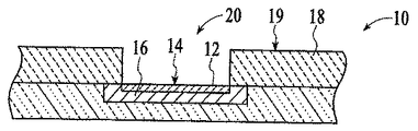
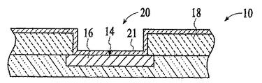
洗浄プロセスは、基板10上の金属含有導体16の表面14を洗浄するために行われる。例えば、洗浄プロセスは、酸素含有環境に表面を晒すことから形成された未変性酸化物膜12のような表面14上に形成された堆積物12を除去するのに有効である。堆積物12は、例えば、炭素、窒素、フッ素、シリコンを含有する残留物のような前のプロセスステップにおいて形成されたプロセス残留物、更に、高分子残留物さえも含み得る。洗浄プロセスは、例えば、銅、アルミニウム、チタン、タングステン、又はその合金又は化合物を含む金属含有導体16の表面14を洗浄することができる。金属含有導体16を含む基板10の実施形態は、図1A-図1Dに示されている。基板10は、下にある金属含有導体16を含み、その上に低k誘電体層18が形成されている。低k誘電体層18は、k値が約2.0〜約3.0のような約3.0未満、更にk値が約2.7未満もの誘電体物質を含んでいる。例えば、適した低k誘電体層は、カリフォルニア州サンタクララのアプライドマテリアルズ社によって製造されたBlackDiamond(登録商標)、低kオキシ炭化シリコンを含むことができる。他の適した低k誘電体層は、シリコンと酸素、炭素、水素及び他の元素の少なくとも1種との組合わせを含むことができる。誘電体層18は、図1Aと図1Bに示されるように、堆積物12を有する金属含有導体16の表面14を露出させる特徴部20を含んでいる。洗浄プロセスは、図1C及び図1Dに示されるように、堆積物12を金属含有導体16の表面14から除去して洗浄された表面14と続いての基板10上に堆積される物質間に良好な電気接触を可能にする。
The cleaning process is performed to clean the
改善された洗浄プロセスが、水素含有ラジカルを含む励起された洗浄ガスに基板10を晒すことを含むことが見出された。水素含有ラジカルは、1つの不対電子を有するので、非常に化学的に反応性であるが、正電荷又は負電荷をもたない水素含有化学種、例えば、水素原子(H・)、ヒドロキシルラジカル(OH・)、窒素含有ラジカル(NH2・、NH3・)、メチルラジカル(CH3・)のような炭素含有ラジカルである。水素含有ラジカルは、未変性酸化物のような堆積物12の酸素成分と化学的に反応することによって比較的緩やかな洗浄プロセスを与えて排気され得る揮発性のヒドロキシルや水蒸気を形成し、それにより堆積物12が金属含有導体16の表面14から除去されると考えられる。従って、励起された水素含有ラジカルは、堆積物12と特に相互作用し、周囲の低k誘電体層18の構造を望ましく損傷する。例えば、水素含有ラジカル洗浄プロセスの層18のk値の増加は、約0.1未満、更に約0.05未満でさえあってもよい。
It has been found that an improved cleaning process involves exposing the
対照的に、正電荷又は負電荷を有する水素含有化学種である水素含有イオンはしばしば基板10エネルギー的に衝突するので、低k誘電体層18の構造を過度に損傷させるとともに層18のk値を増加させ得る。従って、改善された洗浄プロセスは、水素含有ラジカルを含み、ほとんど水素含有イオンを含まない励起ガスに基板10を晒すことが望ましい。例えば、励起洗浄ガスにおける水素含有ラジカルと水素含有イオンの適切な比率は、少なくとも約10,000:1であってもよい。
In contrast, hydrogen-containing ions, which are positively or negatively charged hydrogen-containing species, often energetically impinge on the
励起洗浄ガスは、例えば、一つ以上のH2、H2O、NH3及びSiH4の1種以上の適切な水素含有ガスにエネルギーを結合することによって形成される。多くの水素含有ラジカルを形成するために、洗浄ガスは大部分の水素含有ガス成分を含むことが望ましい。例えば、洗浄ガスは、少なくとも約80%容積の水素含有ガス、少なくとも90%容積でさえ、例えば、90%容積のH2を含み得る。適切な容量流量の水素含有ガスは、約100sccm〜約5リットル/分であってもよい。H2Oを供給すると、励起ガスにおける水素含有ラジカルの形成を促進させることができ、チャンバ106aにおける部品の腐食を減少させることもできることが見出された。例えば、洗浄ガスは、約1%〜約20%容積のH2O、例えば、約1%〜約5%容積のH2Oを含むことができる。従って、一変形例においては、洗浄ガスは、約50sccm〜約1000sccmのH2、約300〜約600sccmのH2、約0〜約10sccmのH2O、例えば、約1〜約5sccmのH2Oを含むことができる。
Energized cleaning gas, for example, be formed by coupling energy into one or more H 2, H 2 O, 1 or more suitable hydrogen-containing gas of NH 3 and SiH 4. In order to form many hydrogen-containing radicals, it is desirable for the cleaning gas to contain a majority of hydrogen-containing gas components. For example, the cleaning gas may comprise at least about 80% volume hydrogen-containing gas, even at least 90% volume, for example 90% volume H 2 . A suitable volumetric flow rate of hydrogen-containing gas may be from about 100 seem to about 5 liters / minute. It has been found that supplying H 2 O can promote the formation of hydrogen-containing radicals in the excitation gas and can also reduce corrosion of components in the
一変形例においては、洗浄ガスは窒素含有ガスを含んでいる。例えば、洗浄ガスは、水素ラジカルと窒素ラジカルの双方を得るために解離するガス組成物を含むことができる。窒素を含む適切な洗浄ガス組成物の例としては、(i)NH3、(ii)NH3とH2O、(iii)N2とH2、(iv)N2と、H2と、H2O、(v)NH3と、H2OとH2を挙げることができる。一変形例においては、洗浄ガスは、約80%〜約100%容積のH2、約1%〜約20%容積のH2O、約1%〜約20%容積のNH3を含んでいる。洗浄ガスは、また、層18からエッチングされた炭素を補充するために炭素源を供給することにより低k誘電体層18を保護するために炭素含有ガスを含むことができる。適した炭素含有ガスの例としては、CO、CH4、CO2及びC2H6の少なくとも1種を挙げることができる。洗浄ガスは、また、N2、Ar、He及びNeの少なくとも1種のような追加ガスを含むこともできる。
In one variation, the cleaning gas includes a nitrogen-containing gas. For example, the cleaning gas can include a gas composition that dissociates to obtain both hydrogen radicals and nitrogen radicals. Examples of suitable cleaning gas compositions containing nitrogen include (i) NH 3 , (ii) NH 3 and H 2 O, (iii) N 2 and H 2 , (iv) N 2 , H 2 , H 2 O, (v) NH 3 , H 2 O and H 2 can be mentioned. In one variation, the cleaning gas comprises about 80% to about 100% volume H 2 , about 1% to about 20% volume H 2 O, about 1% to about 20% volume NH 3 . . The cleaning gas can also include a carbon-containing gas to protect the low-
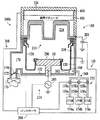
洗浄ガスは、例えば、図2Aに示されるように、遠隔ゾーン30においてガスにエネルギーを結合することによって励起させることができ、それにより、励起されたイオン種とラジカル種を含む遠隔励起ガスが形成される。遠隔ゾーン30は洗浄チャンバ106aのプロセスゾーン108から離れた適切な距離に位置し、遠隔ゾーン30で形成された励起イオン種の多くがプロセス領域108に到達する前に再結合する。ラジカル種は頻繁に再結合せず、平均寿命が同じ距離でイオン種より長いので、遠隔ゾーン30において励起ガスを形成すると、プロセスゾーン108に搬送すべきラジカル種の数が多くなり、イオン種が少なくなることが可能である。遠隔ゾーン30は、プロセスゾーン108から距離dに配置され、距離d全体の遠隔励起ガスの行程、例えば、遠隔ゾーン30からガス分配プレート72までが、ガスをろ過してイオン種の数が減少し、且つラジカル種の数とイオン種の数の比率が高い、励起ガスになる。洗浄チャンバ106aのプロセスゾーン108から遠隔ゾーン30の適切な距離は、例えば、少なくとも約1.5インチ(3.8cm)、例えば、約1インチ(2.5cm)〜約4インチ(10cm)であってもよい。
The cleaning gas can be excited, for example, by coupling energy to the gas in the
その後、活性洗浄ガスは、遠隔励起ガスをろ過するイオンフィルタ50を通過させて遠隔ゾーン30で形成された化学種の比率と異なるイオン水素含有化学種とラジカル水素含有化学種の比率を有するろ過された励起ガスを形成する。望ましくは、イオンフィルタ50が励起洗浄ガスにおけるイオン種の数を減少させて、遠隔ゾーン30で形成されたろ過されていない励起ガスの比率より低いろ過ガスにおけるイオン種とラジカル種の比率を得る。ろ過された励起ガスにおけるイオン種とラジカル種の比(Rf)は、少なくとも約1:100、例えば、少なくとも1:500、少なくとも約1:10,000だけろ過されていない比(Rl)より少なくすることができる。ろ過されていない比率(R1)値は、ろ過された比率(Rf)の少なくとも約100倍、例えば、ろ過された比率の少なくとも約500倍、ろ過された比率の少なくとも約10,000倍さえであってもよい。例えば、ろ過された比率は、Rf=(Rf/R1)・R1に等しくなることができる。ここで、ろ過された比率はRf=If/Nfであり、ろ過されていない比率はR1=I1/Niであり、lfとl1はそれぞれろ過されたガスとろ過されていないガスのイオン数であり、NfとNiはそれぞれろ過されたガスとろ過されていないガスのラジカル種の数がである。イオン種とラジカル種の数によって記述されると、ろ過された比率はRf=(lf/Nf)(Ni/li)・Riと等しい。ろ過されたガスとろ過されていないガスにおけるラジカル種の数がほぼ同じであることを前提とすると、即ち、ラジカルの数は約20%未満だけ変化し、そのときNfはNiに等しく、これらの因子は方程式から取り消され、Rf=(lf/li)Riに等しいろ過された比率が残る。そのようにろ過された比率は、ろ過されたイオンの数とろ過されていないイオン数の比率(lf/li)とほぼ等しい倍率だけ減少したろ過されていない比率に等しくなることができ、望ましくは、約1:100未満、例えば、約1:500未満、約1:10,000未満もの比である。このように、基板10を洗浄するために励起された洗浄ガスにラジカル種が残ることを可能にしつつ、イオンフィルタ50がさもなければ低k誘電体層188に損傷を与えることができる励起ガスからイオン種を除去する。
The active cleaning gas is then filtered through an
所望された比率が得られたかを求めるために励起ガスにおけるイオン種とラジカル種の相対比率を検出するいくつかの方法がある。プラズマ放射を用いた水素ラジカルの相対量は、例えば、656nmで水素放出スペクトルの強度を検出することによってモニタすることができる。励起ガスにおける水素ラジカルの相対量は、通常水素放出ラインの強度に比例するので、放出ライン強度が高いほど水素ラジカル相対濃度が高いことが示される。励起ガスにおける水素イオンの相対量は、例えば、基板支持体110のDCバイアスの変化を測定することによって測定することができる。支持体110上に衝突させ帯電するプラズマの水素の数は、支持体110で測定されたDCバイアスに比例している。このように、支持体110で測定されたDCバイアスと水素放出ライン強度の比率によって、励起されたガスにおけるイオン水素含有化学種とラジカル水素含有化学種の比率を概算することができる。水素イオン濃度は、先端に衝突したイオンによって与えられる電荷からのイオン電流フラックスのようなパラメータを測定するために励起されたガスに挿入される導電性プローブの先端を備えているラングミュアプローブで測定することができる。ラングミュアプローブの例は、Carlileらの米国特許第5,339,039号に記載され、この開示内容は本明細書全体で援用されている。
There are several ways to detect the relative ratio of ionic and radical species in the excitation gas to determine if the desired ratio has been obtained. The relative amount of hydrogen radicals using plasma radiation can be monitored, for example, by detecting the intensity of the hydrogen emission spectrum at 656 nm. Since the relative amount of hydrogen radicals in the excitation gas is generally proportional to the intensity of the hydrogen release line, the higher the release line intensity, the higher the hydrogen radical relative concentration. The relative amount of hydrogen ions in the excitation gas can be measured, for example, by measuring a change in the DC bias of the
水素放出強度の1つ以上、DCバイアス、ラングミュアプローブ又は他の方法を用いてラジカル種及びイオン種の少なくとも1種の相対量と濃度を測定することができる検出器202が設けられる。検出器202は、その領域におけるイオン及びラジカルの少なくとも1種の濃度を測定するためにチャンバ106と装置102の異なる領域に位置させることができる。検出器202は、ろ過されていない励起ガスのラジカル及びイオンの1種以上の量を検出するために遠隔チャンバ40内又はその周りに位置させることができる。例えば、ろ過されていない励起ガスのイオンの検出濃度は、約1011〜約1012イオン/cm3オーダーであってもよい。検出器202は、ろ過されたガスにおけるイオン及びラジカルの1種以上の量を検出するために、例えば、プロセスゾーン108近傍にチャンバ106の周りに位置させることもできる。例えば、ろ過された励起ガスにおけるイオンの検出濃度は、約108〜約109イオン/cm3オーダーであってもよい。従って、装置102の異なる領域におけるイオン種及びラジカル種の少なくとも1種の数は、ろ過されたガスとろ過されていないガスにおけるイオン種とラジカル種の相対量を求めるために検出器102によって測定することができる。
A
一変形例においては、イオンフィルタ50は、図2Aと図2Bに示されるように、励起洗浄ガスが通過することができるその中に開口54を有する導電性ワイヤグリッド52を備えている。ワイヤグリッド52は電気的に接地し得る(図示されるように)のでグリッド52上に衝突したイオン種からの電荷がグリッド52を通って接地電位に伝わり、それによって帯電イオン種が励起洗浄ガスから除去される。ワイヤグリッド52は、帯電されたイオン種に反発する電位ゾーンを生じるように任意にバイアスをかけることもできる。ワイヤグリッド52は、それを通る良好なガスフローを可能にするのに十分に高い開口54の面積とワイヤグリッド52の面積比、例えば、約10:1〜約1:10の比、少なくとも1:1さえも含んでいる。ワイヤグリッド52は、例えば、モリブデン、チタン、ニッケルクロム合金及びアルミニウム合金の少なくとも1種の適切な導電性物質を含んでいる。
In one variation, the
ワイヤグリッド52は、例えば、プロセスゾーン108上の遠隔ゾーン30と基板10間の活性洗浄ガスの流路内に配置されている。一変形例においては、図2Aと図2Bに示されるように、ワイヤグリッド52は、プロセスゾーン108に遠隔ゾーン30から受容した励起洗浄ガスを分配するガス分配プレート72上に取り付けられている。ワイヤグリッド52はガス分配プレート72上に取り付けられ、ワイヤグリッドにおける開口54は、ワイヤグリッド52とガス分配プレート72を通って励起洗浄ガスフローを可能にするためにガス分配プレート72におけるアパーチャ71と一致している。ワイヤグリッド52は、ガス分配プレート72の上面73上に取り付けられ、ワイヤグリッド52の腐食を抑制するために図2Aに示されるようにガス分配プレート72に少なくとも部分的に埋込まれることさえもできる。ガス分配プレート72は、アルミナ、サファイア、シリカ及び石英の少なくとも1種のような誘電性物質、シリコン、アルミニウム及び炭化シリコンのス1種のような導電性物質を含むこともできる。ワイヤグリッドは、更に又は或いは、ガス分配プレート72の底面75に取り付けることができ、又はガス分配プレート72から隔置することもできる。また、プレート72が励起ガスフローをそれを通って巻き込んでいるバッフルとして働くので、ガス分配プレート72はそれ自体イオンフィルタ50として作用することができ、それにより励起ラジカル種の再結合を促進させる。
For example, the
励起洗浄ガスは、石英を含む表面60上に励起ガスを通すことによってイオン種を除去するようにろ過することができる。石英表面60は、水素含有種が水素結合し、表面60に吸着することができる表面を設けることによってラジカルの再結合を減少させるためにイオンフィルタ50として作用すると考えられる。石英表面60上に衝突する水素含有化学種は、吸着した水素含有ラジカルを励起ガスに放出し、それにより水素ラジカルが再生する。水素イオンは、石英表面60によって再生されないので、これらイオンは再結合して電気的に中性の非イオン種を形成する。このように、活性洗浄ガスを石英表面上に通ることにより、イオン種は励起洗浄ガスから効果的にろ過され、ラジカル種は保存される。
The excited cleaning gas can be filtered to remove ionic species by passing the excited gas over a
石英表面60は、励起洗浄ガスから水素イオン種を最適にろ過するように配置されることができる。一変形例において、石英表面60は、図2Aに示されるように、遠隔ゾーン30とプロセスチャンバ100間で接続コンジット62の一部の内部表面を含んでいる。例えば、接続コンジット62は石英チューブから構成することができる。他の変形例においては、石英表面60は、図2Aにも示されるように、ガス分配器70の1つ以上の表面を含んでいる。例えば、ガス分配器70は、石英を含んでいるガス分配プレート72を含むことができる。石英表面60は、ガス分配プレート72とガス分配器流入口83との間にあるガス分配プレナム76を取り囲んでいる壁78、80の表面上にあり得る。例えば、上部と側部のプレナム壁78、80は石英から製造され得る。プレナム壁78、80は、壁78、80を並べたライナ82を含むこともでき、石英ラインのような石英表面60を含むこともできる。石英表面60を含むライナ82は、チャンバ側壁114、底面壁116、シーリング118、ガス分配プレート72のような他のコンポーネントの少なくとも一部の表面のような、チャンバ100内に他の表面を裏打ちすることもできる。
The
基板10の温度は、堆積物12における酸化物の低減に最適条件を与えるように設定され、水素含有ラジカルと堆積物12間の化学反応を促進させるようにさえ設定することができる。例えば、基板の温度は約0℃〜約500℃、例えば、約150℃〜約450℃、約25℃〜約350℃にさえ、例えば、約150℃〜約350℃に維持することができる。一変形例においては、高バイアス電力レベルが励起洗浄ガスにおけるイオンによって基板10の衝突を増加させることができるので、洗浄プロセス中に基板10に印加されるバイアス電力レベルは望ましくは低くてもよい。適切なバイアス電力レベルは、約100ワット未満、例えば、約0〜10ワット、約1ワット〜約10ワットにさえしてもよく、実質的に0にさえすることができる。他の変形例においては、100ワットより大きい、約100ワット〜約200ワットものバイアス電力レベルのような高いバイアス電力レベルは洗浄速度を増加するために適用することができる。
The temperature of the
基板10の洗浄が、熱処理又はアニールステップを行って基板10から堆積物12を除去することにより改善し得ることが更に見出された。熱処理ステップにおいて、基板10は、例えば、堆積物12を揮発させることにより、基板10から物質を脱ガスするのに十分に高い温度に加熱する。基板10上の酸化物の形成を阻止するために熱処理ステップの間、還元ガスのフローを供給することもできる。適切な還元ガスは、例えば、H2のような水素含有ガスを含むことができる。熱処理ステップは、遠隔励起水素ラジカル洗浄ステップの前に、基板10の比較的緩やかな初期洗浄を与えるために、実質的に還元ガスを励起させずに、例えば、実質的に還元ガスにRF又はマイクロ波エネルギーを結合せずに行うことができる。
It has further been found that the cleaning of the
熱処理ステップの一変形例においては、基板10は、少なくとも約100℃、例えば、約150℃〜約350℃の温度に加熱される。H2フローは、約1000sccm〜約5リットル/分の容量の流量で供給される。熱処理ステップ中の圧力は、約100mTorr〜約100Torr、約30Torr未満にさえ維持することができ、適切な加熱時間は約1分〜10分であってもよい。
In one variation of the heat treatment step, the
一変形例においては、熱処理ステップは水素ラジカル洗浄ステップと同じチャンバ106aで行われる。例えば、チャンバ106aは、温度制御システム140とチャンバ106a内で基板10を加熱するように適合されたヒータ142を含むことができる。図2Aに示された実施形態においては、ヒータ142は基板支持体110の基板10の下に抵抗加熱素子111を含んでいる。ヒータ142は、例えば、頭上式加熱ランプ143の、他の加熱デバイスを含むこともできる。他の変形例においては、熱処理ステップは、別個の熱処理チャンバ106c内で行われ、その実施形態は図2cに示されている。熱処理チャンバ106cは、例えば、真空搬送チャンバ117によって洗浄チャンバ106aと真空接触していることが望ましく、基板10が加熱プロセスチャンバ106cから洗浄チャンバ106aまで真空を破壊することなく搬送され得る。
In one variation, the heat treatment step is performed in the
一実施形態においては、下にある低k誘電体層18の表面19を露出するためにほぼ完全にレジスト層22が除去された後、洗浄プロセス、任意の熱処理プロセスが行われる。ストリッピングプロセスは、図1Aに示されるように、レジスト層22を含む基板10をストリッピングチャンバにおいて酸素含有ガスのような励起ストリッピングガスに晒すことを含むことができる。一旦レジスト層22のストリッピングが完了し、図1Bに示されるように、レジスト層22はほぼ完全に除去されると、基板10は別個の洗浄チャンバ106aに搬送される。ストリッピングプロセスが基板10から大量の物質の除去を必要とすることがあり、ストリッピングチャンバと洗浄チャンバ106a又は他のチャンバとの真空統合によってストリッピングチャンバからの汚染を生じ得るので、洗浄チャンバ106aは、ストリッピングチャンバと真空接触していない別個のマルチチャンバ装置の一部であることが望ましい。別個の熱処理チャンバ106cが用いられる場合、熱処理チャンバ106cは、ストリッピングチャンバと真空接触していないことが望ましく、洗浄チャンバ106aを含むマルチチャンバ真空装置の一部であり得る。堆積物12の未変性酸化物成分は、図1Bに示されるように、酸素含有ストリッピング環境に金属含有導体16を晒す際に、又はストリッピングチャンバから洗浄チャンバ106aへの基板10の搬送中に周囲雰囲気に晒す際に、金属含有導体16の表面14上に形成し得る。
In one embodiment, after the resist
適切な洗浄プロセスの一変形例においては、約50〜約1000sccmのH2、例えば、300sccmのH2と約0〜10sccmのH2O、例えば、3scmのH2Oを含む洗浄ガスは、約300ワット〜約3000ワットの電力レベル、例えば、1050ワットを印加することによってリモートソース35で活性化される。チャンバ圧は、約10Torr未満、例えば、約1Torrに維持される。約0〜約100ワットのバイアス電力レベル、例えば、50ワットは、基板10にバイアスをかけるために印加され、基板10の温度は、約150〜約450℃、例えば、250℃に維持される。洗浄プロセスは、図1Cに示されるように、堆積物12をほぼ除去し、洗浄された表面14が得られる。
In one variation of a suitable cleaning process, a cleaning gas comprising about 50 to about 1000 sccm H 2 , for example 300 sccm H 2 and about 0 to 10 sccm H 2 O, for example 3 scm H 2 O, is about It is activated at the
洗浄プロセスが完了した後、チャンバ106a内の圧力は廃洗浄ガスと洗浄副生成物を排気するとともに洗浄チャンバ106aのそばのマルチチャンバ装置汚染の可能性を減少させるために約10mTorr未満に減圧される。その後、基板10は、図1Dに示されるように、新たに洗浄された金属含有導体表面14上に、銅、アルミニウム、タンタル、タングステン、窒化タンタル及び窒化タングステンの少なくとも1種のような第二金属含有導体21を堆積するために搬送ロボット119を有する基板搬送チャンバ117によって減圧下で堆積チャンバ106bに搬送され得る。
After the cleaning process is complete, the pressure in the
水素含有ラジカル洗浄プロセスに適した洗浄チャンバ106aを含む装置102の実施形態は、図2Aに示されてる。本明細書に示される装置102の具体的な実施形態は、半導体ウェハのような基板10を洗浄するのに適し、フラットパネルディスプレイ、ポリマーパネル、又は他の電気回路受容基板10のような他の基板10を洗浄するために当業者によって適合させることができる。一般的に、洗浄チャンバ106aは、エンクロージャーのような1つ以上の壁107を含み、プロセスゾーン108を封じるシーリング118、側壁114、底面壁116を含むことができる。励起洗浄ガスは、リモートソース35とガス分配器70を含むガス供給源130によってプロセスゾーン108に供給される。洗浄ガスは、リモートソース35によって励起され、流入口83を有する接続コンジット62を経てガス分配器70に受容される。ガス分配器70は、プロセスゾーン108にガスを分配するためにその中にアパーチャ71を有するガス分配プレート72を含み得る。ガス分配器70は、また、基板10の周辺に1つ以上のコンジットを任意に含むことができる。廃ガスや副生成物は、プロセスゾーン108からガスを受容する排気ポート177を含むことができる排気システム144を通ってチャンバ106aから排気され、チャンバ106a内のガス圧を制御するためにスロットルバルブ135と、1つ以上の排気ポンプ152、例えば、ターボ分子排気ポンプを更に含むことができる。排気システム144は、チャンバ106aの大気圧未満を維持することができる。
An embodiment of an
洗浄ガスを遠隔励起するのに適したリモートソース35は、遠隔ゾーン30、洗浄ガスソース39、リモートガスエナジャイザー37を有するリモートチャンバ40を含んでいる。動作中、洗浄ガスはリモートチャンバ40における洗浄ガスソース39から受容する。リモートチャンバ40への洗浄ガスの流量を制御するためにフローバルブ41を設けることができる。リモートガスエナジャイザー37は、遠隔ゾーン30で洗浄ガスにエネルギーを結合して洗浄ガスを励起し、それにより励起イオン種とラジカル種を含む励起洗浄ガスが形成される。リモートガスエナジャイザー37は、例えば、洗浄ガスにRFとマイクロ波エネルギーの少なくとも1種を結合することができる。一変形例においては、リモートガスエナジャイザー37は、遠隔領域30における洗浄ガスにRFエネルギーを誘導結合させる誘導アンテナを含んでいる。洗浄ガスに結合するのに適したRF電力レベルは、約100ワット〜約10kワットであってもよい。他の変形例においては、リモートガスエナジャイザー37は、例えば、Smithらの米国特許第6,150,628号に記載されるように、遠隔ゾーン30で洗浄ガスにエネルギーを結合するトロイダル型ガスエナジャイザーを含んでいる。その特許の開示内容は本明細書全体に援用されている。トロイダル型ガスエナジャイザーによって印加された適切なRF電力レベルは、約1000ワット〜約10,000ワットであってもよい。マイクロ波ガスアクチベータを含むリモートガスエナジャイザー37を設けることもできる。適切なマイクロ波電力レベルは、約300ワット〜約5kワットであってもよい。チャンバ106aは、チャンバ106aのプロセスゾーン108においてガスにエネルギーを結合するチャンバガスエナジャイザーを任意に含むこともできる。例えば、チャンバガスエナジャイザーは、RFエネルギーを結合させる電極及び誘導アンテナの1種以上を含むことができる。
A suitable
基板10は、基板受容表面180を有する支持110上のプロセスゾーン108に保持される。支持体110は、電圧源91から電力レベルを印加することによって電気的にバイアスをかけ得る電極90を任意に含むことができる。電極90は、支持体110上の基板10を静電的に保持するためにバイアスをかけることができる。電極90と基板10は、プロセスの特性、例えば、基板10へのイオン衝撃の程度に影響するようにバイアスをかけることも可できる。しかしながら、支持体110はいかなる帯電可能電極を存在しないこともあり得る。温度制御システム140は、基板10の温度を維持するために設けられ、例えば、基板10の下の支持体110に抵抗加熱素子111を含むことができる。温度制御システム140は、1種以上の他の熱交換デバイス、例えば、熱交換流体が供給される熱交換コンジットや加熱ランプを含むこともできる。温度制御システム140は、基板10の温度をモニタするとともにチャンバコントローラ300に温度に関して信号を送る熱電対のような温度モニタを含むこともできる。
The
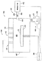
プロセスチャンバ195を含む装置102は、複数のプロセスチャンバ106a‐dを含む大きなマルチチャンバ装置102の一部でもあり得る。基板10を処理するのに適した装置102の実施形態は、図3に示されるように、1つ以上のプロセスチャンバ106a−dを含んでいる。チャンバ106a‐dは、電気プラミング、及び他の支持機能を設ける、カリフォルニア州サンタクララのアプライドマテリアルズ社からPrecision5000(登録商標)のようなプラットフォーム上に取り付けられる。プラットフォーム109は、典型的には、処理すべき基板10のカセット115を受容するロードロック113と処理するためにカセット115から異なるチャンバ106a‐dに基板を搬送するとともにプロセス後に基板を戻すためにロボット119を含む基板搬送チャンバ117を支持する。異なるチャンバ106a‐dは、例えば、堆積洗浄チャンバ106a、ウエハ上に物質を堆積するための堆積チャンバ106b、任意に、熱処理チャンバ106c、他処理チャンバを含むことができる。例えば、一変形例においては、チャンバ106a‐dの一つは、基板10上の金属含有導体16上に形成された堆積物12を除去するための洗浄チャンバ106aを含んでいる。洗浄プロセスが終了した後、基板10は洗浄された基板上の金属含有導体のような物質を堆積する堆積チャンバ106bにロボット119によって搬送され得る。基板10は、第一チャンバ内で堆積された第一物質上に、他の金属含有導体のような他の物質を堆積することができる第二堆積チャンバ106にロボット119によって搬送され得る。また、熱処理プロセス後、基板10は、ロボット119によって熱処理チャンバ106cから洗浄チャンバ106aに搬送され得る。チャンバ106a‐dは、プロセスが連続して処理することができる装置102内で連続真空環境を形成するために相互接続され、それにより異なるプロセス段階の別個のチャンバ間でウェハを搬送する場合に生じることがある基板10の汚染が減少する。搬送チャンバ117は、チャンバ106a‐dの汚染を減少させるために、ガスを排気するとともに低圧環境、例えば、約10mTorr未満の圧力を維持する流出口129を有する排気システムを備えている。
The
基板10上に物質を堆積することができるチャンバ106bの例示的な変形例は、図4Bに概略的に示されている。チャンバ106bは、代表的な自己イオン化プラズマチャンバ、例えば、カリフォルニア州サンタクララのアプライドマテリアルズ社によって開発されたSIP+型チャンバである。しかしながら、本発明の態様は、SIP+型チャンバを含む堆積チャンバに限定されず、他の堆積チャンバも適している。典型的なチャンバ106bは、側壁120、底面壁122、シーリング124を含むエンクロージャー218を含んでいる。基板支持体230は、チャンバ106b内で基板10を支持するために設けられている。基板支持体230は、例えば、RF電源203であってもよい、ペデスタル電源210によって電気的に浮動してもバイアスがかけられてもよい。基板10は、チャンバ106bの側壁120にある基板装填流入口(図示せず)を通ってチャンバ106b内に導入され、支持230上に配置される。支持体230は、支持リフトベローズ(図示せず)によって持ち上げることも下げることもでき、リフトフィンガーアセンブリ(図示せず)は、チャンバ106b内外へ基板10の搬送中に支持体230に基板10を持ち上げ、下げるために使用し得る。
An exemplary variation of the
スパッタリングガスのようなプロセスガスは、それを通って設定流量ガスを通過させるマスフローコントローラのようなガスフロー制御バルブ158a‐cを有するコンジット156a‐cにそれぞれ送り込むガスソース154a‐cを含むプロセスガス供給源252を通ってチャンバ160bに導入される。コンジット156a‐cによって、ガスが所望のプロセスガス組成物を形成するように混合される混合マニホールド160にガスが送り込まれる。ガス流出口164は、基板支持体230の周辺を完了するためにチャンバ側壁120を通過することができる。プロセスガスは、ターゲット211上に励起的に衝突させるとともにターゲット211から物質をスパッタする、アルゴン又はキセノンのような非反応性ガスを含むことができる。プロセスガスは、基板10上に層を形成するためにスパッタされた物質と反応することができる酸素含有ガス及び窒素含有ガスの1種以上のような反応性ガスを含むこともできる。廃プロセスガスや副生成物は、廃プロセスガスを受容する1つ以上の排気ポート170を含む排気システム168を通ってチャンバ106bから排気され、チャンバ106bにおけるガスの圧力を制御するスロットルバルブ174がある排気コンジット172に廃ガスを移すことができる。排気コンジット172によって、1つ以上の排気ポンプ176に送り込まれる。典型的には、チャンバ106bにおけるスパッタリングガスの圧力は、大気圧未満レベルに設定される。
A process gas supply, including a
スパッタリングチャンバ106bは、更に、基板10と向いたスパッタリングターゲット211を含んでいる。スパッタリングターゲット211は、図4Bに示される形状のような所望の形状を含むことができる。スパッタリングターゲット211は、ほぼ平面のスパッタリング表面をもつほぼ平面の形状を備えることもできる。スパッタリングチャンバ106bは、スパッタされた物質からチャンバ106bの壁218を保護するとともに、典型的には、カソードターゲット211についてアノードとしても働くシールド128を備えることもできる。シールド128は、電気的に浮動していても接地されてもよい。ターゲット211は、チャンバ106bから電気的に分離され、パルスDC電源のようなターゲット電源201に接続されるが、他のタイプの電圧源であってもよい。一変形例においては、ターゲット電源201、ターゲット211、シールド128は、ターゲット211から物質をスパッタするためにスパッタリングガスを励起することができるガスエナジャイザー180として作動させる。ターゲット電源201は、シールド128に相対してターゲット211にバイアス電圧を印加する。スパッタリングターゲット211に印加された電圧からチャンバ106b内に生成された電界は、ターゲットから、また、基板10上に物質をスパッタさせるためにターゲット211上に励起的に衝突させ、それに衝突させるプラズマを形成するためのスパッタリングガスを励起させる。プロセスガスを励起させるためのパルスDC電圧の適したパルス周波数は、例えば、少なくとも約50kHz、更に好ましくは約300kHz未満であり、最も好ましくは約100kHzであってもよい。プロセスガスを励起させるために適したDC電圧レベルは、例えば約200〜約800ボルトであってもよい。
The sputtering
チャンバ106bは、チャンバ106bのターゲット211近傍に磁界を生成して、ターゲット211に隣接した高密度プラズマ領域226におけるイオン密度を増加させて、ターゲット物質のスパッタリングを改善する、磁界ゼネレータ401を含むマグネトロン403を更に含んでいる。改善されたマグネトロン403は、例えば“回転スパッタマグネトロンアセンブリ”と称するFuの米国特許第6,183,614号、 “銅バイア充填のための集積化プロセス”と称するGopalrajaらの米国特許第6,274,008号に記載されるように、ターゲット衝突のために非反応性ガスの要求を最少にしつつ、銅の自己スパッタリング、又はアルミニウム、チタン又は他の金属のスパッタリングを持続させるために用いることができる。それらの特許は共に本明細書に全体で援用されている。
The
任意の熱処理チャンバ106cの実施形態は図4Bに示されている。熱処理チャンバは、プロセスゾーン408を封じるエンクロージャー壁407を備えている。熱処理ガスは、例えば、熱処理ガス源432や接続コンジット436を通って供給源から熱処理ガスを受容するガス分配器434を備えている、ガス分配システム430によってプロセスゾーン408に供給される。ガス分配システム430は、プロセスゾーン408へのガスフローを制御するためにフローメータ438を更に備えることができる。基板10は、支持体410上のプロセスゾーン408に保持される。支持体410は、支持体410上に基板10を保持させるために電気的にバイアスをかけ得る電極(図示せず)を任意に備えていてもよい。廃ガスや副生成物は、プロセスゾーン408からガスを受容する排気ポート477を含むことができる排気システム444を通ってチャンバ106cから排気され、チャンバ106aにおけるガス圧を制御するスロットルバルブ435と、ターボ分子排気ポンプのような1つ以上の排気ポンプ452を含むこともできる。
An optional
加熱プロセスチャンバ106cは、所望の温度に基板10を加熱するとともに基板10を所望の温度で維持することができるヒータ142を有する温度制御システムを備えている。図4Aに示されるような実施形態においては、ヒータ142は、基板10の表面上に熱放射を送るように適合された加熱ランプ143のアレイ445を備えている。温度制御システム140は、支持体410における抵抗加熱素子又は熱交換流体を供給する熱交換コンジットのような1つ以上の他の加熱デバイスを備えることもできる。温度制御システム140は、基板10の温度をモニタするとともにチャンバコントローラ300に温度に関する信号を送る熱電対のような温度モニタを備えることもできる。
The
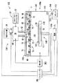
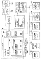
マルチチャンバ装置102は、図5に示されるように、ハードウェアインタフェース304を経てコントローラ300によって作動させることができる。コントローラ300は、例えば、カリフォルニア州のシナジーマイクロシステムズ社から市販されている680640マイクロプロセッサ、又はカリフォルニア州サンタクララのインテル社から市販されているペンティアムプロセッサのような中央プロセッサ装置(CPU)306を有するコンピュータ302を備え、メモリ308と周辺コンピュータコンポーネントに結合されている。好ましくは、メモリ308は、例えば、CD又はフロッピードライブの交換可能記憶媒体310、例えば、ハードドライブの交換不可記憶媒体312、ランダムアクセスメモリ314を含むことができる。コントローラ300は、例えば、アナログやデジタルの入力や出力のボードを含む複数のインタフェースカード、インタフェースボード、モータコントローラボードを更に備えることができる。オペレータとコントローラ300間のインタフェースは、例えば、ディスプレイ316やライトペン318であり得る。ライトペン318は、ライトペン318の先端の光センサでモニタディスプレイ316によって出される光を検出する。具体的なスクリーン又は機能を選択するために、オペレータはモニタ316上のスクリーンの明示領域に触れ、ライトペン318でボタンを押す。典型的には、触れた領域は色が変わるか、又は新しいメニューが表示され、ユーザーとコントローラ300間の情報が確認される。
The
一変形例においては、コントローラ300は、例えば、交換不可記憶媒体312又は交換可能記憶媒体310のメモリ308に保存することができるコンピュータ読取り可能プログラム320を備えている。コンピュータ読取り可能なプログラム320は、通常は、例えば、チャンバ106a‐dとそれらのコンポーネント、搬送チャンバ117、ロボット119を作動させるプログラムコードを備えているプロセス制御ソフトウェア、チャンバ106a‐dで行われるプロセスをモニタするプロセスモニタリングソフトウェア、安全システムソフトウェア、他の制御ソフトウェアを備えている。コンピュータ読み取り可能なプログラム320は、従来の任意のコンピュータ読取り可能なプログラミング言語、例えば、アセンブリ言語、C++又はFortanで書き込むことができる。適切なプログラムコードは、従来のテキストエディタを用いメモリ308のコンピュータ使用可能な媒体において保存又は具体化されたシングルファイル又はマルチファイル内に入力される。入力されたコードテキストが高級言語である場合には、コードはコンパイルされ、その後、得られたコンパイラコードがプリコンパイルされたライブラリルーチンのオブジェクトコードにリンクされる。リンクされコンパイルされたオブジェクトコードを実行するために、ユーザーはオブジェクトコードを呼び出し、CPU306がコードを読み込み実行させてプログラムで同定されたタスクを行う。
In one variation, the
コンピュータ読取り可能なプログラム320の個々の実施形態の階層制御構造の説明的ブロックダイアグラムは、図10に示されている。ライトペンインタフェースを用いて、ユーザーはCRTターミナルに表示されたメニュー又はスクリーンに応答してコンピュータ読取り可能なプログラム320にプロセス設定とチャンバ番号を入力する。コンピュータ読取り可能なプログラムは、基板位置、ガスフロー、ガス圧、温度、RF電力レベル、、具体的なプロセスの他のパラメータ、チャンバプロセスをモニタするコードを制御するためのプログラムコードを含んでいる。プロセス設定は、指定されたプロセスを行うのに必要なプロセスパラメータの所定のグループである。プロセスパラメータは、ガス組成、ガス流量、温度、圧力、RF電力レベルのようなガスエナジャイザー設定を含むがそれらに限定されないプロセス条件である。
An illustrative block diagram of the hierarchical control structure of an individual embodiment of a computer
プロセスシーケンサプログラムコード322は、コンピュータ読取り可能なプログラム320からチャンバの種類とプロセスパラメータの設定を受け入れ且つその動作を制御するプログラムコードを備えている。シーケンサプログラムコード322は、プロセスチャンバ106a‐dにおけるマルチプロセスタスクを制御するチャンバマネージャープログラムコード324に具体的なプロセスパラメータを移すことによりプロセス設定の実行を開始する。典型的には、プロセスチャンバプログラムコード324には、基板配置プログラムコード326、ガスフロー制御プログラムコード328、ガス圧制御プログラムコード330、温度制御プログラムコード332、ガスエナジャイザー制御プログラムコード334、プロセスモニタリングプログラムコード336が含まれている。
Process
典型的には、基板配置プログラムコード326は、チャンバ106a‐d内で支持体110、230上に基板10を装填し、任意にチャンバ106a‐d内で所望の高さに基板10を持ち上げるために用いられるチャンバコンポーネントを制御するための指示を備えている。基板配置プログラムコード334は、マルチチャンバ装置102におけるチャンバ間で基板10を搬送するために搬送チャンバ117内のロボット119を制御することもできる。ガスフロー制御プログラムコード328は、洗浄ガス、熱処理ガス又はスパッタリングガスのようなプロセスガスの異なる成分の流量を制御するための指示を備えている。ガスフロー制御プログラムコード328は、1つ以上のガスフローバルブ41、158a、c、436の開口サイズを調節してチャンバ106a‐cへの所望のガス流量を得る。
Typically, the substrate
温度制御プログラムコード332は、基板10の温度のようなチャンバ106a‐c内の温度を制御するためのプログラムコードを備えている。例えば、温度制御プログラムコードは、支持体の抵抗加熱素子111のようなヒータ142に加えられる電流を制御するとともに温度センサーから信号をモニタして所望の温度を維持することによって洗浄チャンバ106aにおける基板10の温度を制御し得る。温度制御プログラムコードは、同様に、ヒータ142に加えられた電流を制御するとともに基板温度をモニタすることにより、別個の熱処理チャンバ106cにおいて基板10の温度を制御することができる。ガスネナジャイザ制御プログラムコード334は、例えば、ガスを励起させるために印加された電力レベルを設定することにより、リモートガスエナジャイザー37やスパッタリングガスエナジャイザ180のようなガスエナジャイザーを制御するための指示を備えている。プロセスモニタリングプログラムコード334は、チャンバ106a−cにおけるプロセスをモニタする、例えば、検出器202によってろ過されていない励起ガス及びろ過された励起ガスの1つ以上におけるイオン種とラジカル種の比率をモニタするための指示を備えている。圧力制御プログラムコード330は、例えば、スロットルバルブ174、135、477を制御することによって、チャンバ106a−cや搬送チャンバ117における圧力を制御するための指示を備えている。
The temperature
一変形例においては、コントローラは、洗浄チャンバ106aにおいて堆積物12を基板10上の最初の金属含有伝導帯116から洗浄し、基板10をスパッタリングチャンバ106bに搬送し、且つ第二金属含有導体21を洗浄された第一金属含有導体16上に堆積させるために、洗浄チャンバ106a、スパッタリングチャンバ106b、ロボット119を作動させるプログラムコードを備えている。コントローラ300は、堆積物12を洗浄する洗浄チャンバ106aに基板10を搬送する前に、最初の熱処理ステップを行う熱処理チャンバ106cを作動させるプログラムコードを任意に備えていてもよい。
In one variation, the controller cleans the
コントローラ300よって受容及び/又は評価されたデータ信号は、ファクトリオートメーションホストコンピュータ338に送信することができる。ファクトリオートメーションホストコンピュータ318は、(i)基板10に行われたプロセス、(ii)基板10全体に統計的関係で変化することができる特性、又は(iii)基板10のバッチ全体に統計的関係で変化することができる特性の統計的プロセス制御パラメータを確認するために、いくつかのシステム、プラットフォーム又はチャンバ106a‐dからのデータと、基板10のバッチについて又は長時間にわたるデータを評価するホストソフトウェアプログラム340を備えることができる。ホストソフトウェアプログラム340は、進行中のインサイチュプロセス評価又は他のプロセスパラメータの制御のデータを用いることもできる。適切なホストソフトウェアプログラムは、前述のアプライドマテリアルズ社から入手できるWORKSTREAM(登録商標)ソフトウェアプログラムを備えている。ファクトリオートメーションホストコンピュータ338は、更に、(i)例えば、基板特性が不十分又は統計的に求められた数値の範囲内に入っていない、又はプロセスパラメータが許容範囲からそれている場合には、処理シーケンスから具体的な基板10を取り出す;(ii)具体的なチャンバ106a−dにおけるプロセスを終わらせる、又は(iii)基板10の適していない特性又はプロセスパラメータを求める際にプロセス条件を調節するための指示信号を送るように適合させることができる。ファクトリオートメーションホストコンピュータ338は、ホストソフトウェア340によるデータの評価に応答して基板10の処理の開始又は終了で指示信号を送ることもできる。
Data signals received and / or evaluated by the
実施例
以下の実施例は、励起された水素含有ラジカルによって得られた改善された洗浄結果を示すものである。実施例においては、基板10は、その上に低k誘電体層が形成された銅導体16を備えたものである。銅導体16は、低k誘電体層18における特徴部20まで露出したその上に酸化銅12の層を有した。誘電体層のk値の変化は、Hgプローブを用いて測定した。
Examples The following examples illustrate the improved cleaning results obtained with excited hydrogen-containing radicals. In the embodiment, the
実施例1
本実施例は、異なる厚さの低k誘電体に対する従来の洗浄プロセスによるk値に対する影響を示すものである。従来の洗浄プロセスは、プロセスゾーンにおいて95%のHeと5%のH2を含む洗浄ガスを供給すること;プロセスゾーンにおいて洗浄ガスに450ワットのRF電力レベルを誘導結合させること;チャンバ圧を80mTorrに維持すること;10ワットのバイアス電力レベルを印加すること含んだものである。基板10を洗浄ガスに40秒間晒した。以下の表1は、低k誘電体層の厚さの関数としてk値の変化を示すものである。
Example 1
This example shows the effect on the k value of a conventional cleaning process for different thickness low k dielectrics. A conventional cleaning process supplies a cleaning gas containing 95% He and 5% H 2 in the process zone; inductively coupling a 450 watt RF power level to the cleaning gas in the process zone; a chamber pressure of 80 mTorr Holding a bias power level of 10 watts. The
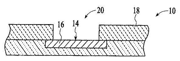
表1は、低k誘電体層18の厚さが減少するにつれて洗浄された基板10のk値の変化が増大することを示している。1500オングストローム以下のような薄い膜厚でのk値の急な増加は、低k誘電体層18の上面19が従来の洗浄プロセスによって最も激しく損傷される領域であるという事実によると考えられる。バルク誘電体層の厚さが減少するにつれて、この上面19のキャパシタンスは層18の全体のキャパシタンスに一層寄与する。従って、従来のプロセスは、低k誘電体層18を有する基板、特に厚さが約1500オングストローム以下の低k誘電体層18を有する基板の十分な洗浄を与えることはできない。
Table 1 shows that the change in the k value of the cleaned
実施例2
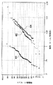
実施例2は、洗浄プロセスに対する種々のプロセスパラメータの影響を示すものである。これらの実施例においては、出発低k誘電体層の厚さが1500オングストロームである基板10は、励起洗浄ガスがプロセスゾーンで形成され且つ洗浄ガスがイオン数を減少させるようにろ過されなかった従来の洗浄プロセスに供された。基板バイアス電力レベル、ガス励起電力レベル、ガス圧を含む種々のプロセスパラメータで多因子試験を行った。図6は、多因子条件下で処理された基板10の低k誘電体層の厚さの変化(Δt)とk値への変化(Δk)を示している。
Example 2
Example 2 shows the effect of various process parameters on the cleaning process. In these embodiments,
図6は、基板バイアス電力レベルがk値の変化と低k誘電体層18の厚さの変化に対して強い影響を有し、しばしば低k誘電体層18からスパッタリングすることにより低下することを示している。ライン501と502が示すように、厚さの変化とk値の変化は、基板10に印加されるバイアス電力レベルが上がるにつれて増大する。対照的に、ガス励起電力レベルと圧力はk値と厚さに強く影響するように見えない。ライン503と504は、増加するガス活性化電力レベルに対して、それぞれ厚さとk値の変化を示している。ライン505と506は、増加する圧力に対して、それぞれ厚さとk値の変化を示している。バイアス電力レベルが増加すると、イオン種による基板10の衝撃が増加する。従って、このデータは、k値の変化の主な要因の1つがイオン種による基板10へ衝撃であることを示している。従って、改善された洗浄プロセスは、洗浄ガスからイオン種をろ過して基板10の衝撃を減少させる。
FIG. 6 shows that the substrate bias power level has a strong effect on the change in k value and the change in the thickness of the low-
実施例3
本実施例においては、洗浄ガス組成が異なる従来の洗浄プロセスから生じるk値の変化を評価した。基板10は、厚さが1500オングストロームの低k誘電体層18を含むプロセスで洗浄した。洗浄プロセスにおいては、表2に挙げた洗浄ガスをプロセスゾーンにおいてガスをエネルギーに結合することによって励起させた。第一洗浄プロセスにおいては、基板バイアス電力レベルは300ワット、ガス圧は0.5mTorrとした。第二洗浄プロセスにおいては、基板バイアス電力レベルは10ワット、ガス圧は80mTorrとした。低k誘電体層のk値の変化パーセントは、各洗浄プロセス後に測定した。洗浄プロセスの結果を、以下表2に示す。
Example 3
In this example, the change in k value resulting from a conventional cleaning process with different cleaning gas compositions was evaluated. The
このように、表2は、タイプの洗浄ガスの種類が異なる従来の洗浄プロセスは、k値が付随し望ましくない増加をせずに基板10の良好な洗浄をもたらすことができないことを示している。k値の増加は、水素含有ガスをによる洗浄プロセスの30%程度増加した。
Ar洗浄ガスプロセスに対するk値変化パーセントは最も小さいが、Arガスはk値の許容できない増加を生じる大きなバイアス電力レベルを印加せずに基板10から金属酸化物をしばしばほとんど洗浄しない。
Thus, Table 2 shows that conventional cleaning processes with different types of cleaning gases cannot provide good cleaning of the
Although the percent change in k value for the Ar cleaning gas process is the smallest, Ar gas often does not clean the metal oxide from the
実施例4
本実施例においては、多数の水素ラジカル含有種を供給して基板10から金属酸化物を洗浄することによる比較的穏やかな洗浄プロセスにより基板10を洗浄した。比較的穏やかな洗浄プロセスは、遠隔ゾーンにおいて励起された水素含有ガスを形成し、ガスにおけるイオン種の数を減少させるとともに多くの水素ラジカル含有化学種を供給するために石英表面60上に励起ガスを通すことにより励起ガスをろ過することを必要とした。基板10は、厚さが1500オングストロームの低k誘電体層18を備えたプロセスで洗浄した。洗浄ガスは3000sccmのH2を含み、洗浄プロセスは以下の表3に挙げたガス励起電力レベルと温度で40秒間行った。誘電体層18のk値の変化を測定し、表3に示す。
Example 4
In this example, the
このように、表1、2、3の比較は、冷機洗浄ガスが多くの水素含有ラジカルを含む洗浄プロセスが、結果としてk値の変化がかなり減少するので、ろ過せずにガス中のイオン種の数を減少させるプロセスより洗浄ガスが改善することを示している。イオン種をろ過しない従来の洗浄プロセスにより、イオン種の数が減少した洗浄ガスプロセスに対するk値の変化パーセントより20倍ほど、30倍さえもあり得るk値の変化パーセントが得られる。従って、低k誘電体層を有する基板10の洗浄改善は、励起水素含有ガスをろ過してガス中のイオン種の数を減少させることにより得ることができ、それにより処理された基板10の品質を改善するとともに厚さが薄い誘電体層18を本質的に層を損傷させずに洗浄させることを可能にする。
Thus, the comparison of Tables 1, 2 and 3 shows that the cleaning process in which the cold cleaning gas contains many hydrogen-containing radicals results in a significant reduction in the change in k value, so that the ionic species in the gas without filtering. It shows that the cleaning gas is improved over the process of reducing the number of the gas. A conventional cleaning process that does not filter ionic species provides a percent change in k value that can be as much as 20 times or even 30 times the percent change in k value for a cleaning gas process with a reduced number of ionic species. Accordingly, improved cleaning of the
実施例5
本実施例は、水素含有ラジカル種を含む励起された洗浄ガスによる基板の洗浄において温度の重要性を示すものである。厚さが1500オングストロームの低k誘電体層を備えた基板10を、1400ワットのマイクロ波電力レベルを印加することによりリモートソース35において3000sccmのH2と30sccmのH2Oを含む洗浄ガスを励起することによって洗浄した。基板10の温度は、以下表4に示されるように、洗浄される各基板10について変化させた。k値を洗浄前後に測定し、k値の変化パーセントを求めた。k値は、洗浄後約3であった。ウェハとウェハ間の変化によるノイズや洗浄される基板が比較的少ないことから、測定されたk値の変化が実際の変化より大きくなり、上記表3に示されたものより大きくなることは留意すべきである。しかしながら、表4は温度の増加によるk値の増加の一般傾向を示している。
Example 5
This example shows the importance of temperature in cleaning a substrate with an excited cleaning gas containing hydrogen-containing radical species.
洗浄された基板の反射率も測定され、反射率パーセントについて図7において基板温度増加をグラフにした。高い反射率は、より多くの未変性酸化物が銅導体16の表面14から除去されたことを示している。ライン507は、洗浄プロセス前の平均反射率であり、ライン508は洗浄プロセス後の平均反射率であり、ライン509とライン510はそれぞれ洗浄プロセス前後の反射率測定の標準偏差パーセントである。このように、基板10の良好な洗浄プロセスは高い温度で得られるが、良好な洗浄プロセスが80℃の低い基板温度でもなお得られることをグラフは示している。従って、表4と図7のグラフは、良好な洗浄プロセス結果が水素含有ラジカルによる洗浄で得ることができることを示し、また、温度が低k誘電体層のk値を過度に上げることなく最適な洗浄を与えるように慎重に選ぶべきであることを示している。
The reflectance of the cleaned substrate was also measured, and the increase in substrate temperature was graphed in FIG. The high reflectivity indicates that more native oxide has been removed from the
実施例6
本実施例は、熱処理ステップを行うことによって得ることができる改善された結果を示すものである。本実施例においては、H2ガスフローを供給しつつ、銅導体16と低k誘電体層18を備えている基板10を少なくとも約100℃の温度に基板を加熱することを含む熱処理プロセスで処理した。その後、熱処理基板10をろ過された水素含有ラジカル種を含む遠隔励起ガスによる洗浄プロセスにおいて洗浄して堆積物12を銅導体16の表面14から除去した。その後、洗浄された表面14上に窒化タンタル層を含む第二金属含有導体21を堆積させるために堆積プロセスを行った。銅と窒化タンタル相互接続特徴部20の電気抵抗について、図8におけるライン600に示されるように、基板10全体の特徴部20を測定した。
Example 6
This example shows the improved results that can be obtained by performing a heat treatment step. In this embodiment, the
熱処理結果を比較するために、基板10を、熱処理ステップを含めずに処理し、基板10全体の特徴部20の電気抵抗を測定した。一プロセスにおいては、基板10上に窒化タンタル層を堆積する前に、別個の熱処理ステップを含めずにろ過された水素含有ラジカルを含む遠隔励起ガスによって基板10を洗浄し、その結果はライン602で示されている。他のプロセスにおいては、前洗浄又は熱処理ステップを行わずに窒化タンタル層を基板10上に堆積し、その結果はライン604で示されている。
In order to compare the heat treatment results, the
図8は、接触抵抗の低い基板20全体の特徴部20の割合は、洗浄し基板上に物質を堆積する前に熱処理ステップで処理された基板については非常に高いことを示している。図8は、抵抗測定値以下の抵抗を有する特徴部の割合を示すグラフであり、測定された抵抗値はグラフのx軸上に示され、特徴部の割合はグラフのy軸上に示されている。ライン600に示されるように、熱処理ステップは、基板全体の約95%より大きい特徴部20について約1オーム/特徴部未満の抵抗を与える。対照的に、熱処理せずに処理された基板10は、抵抗が約1オーム/特徴部未満である特徴部20が約5%未満である。
FIG. 8 shows that the percentage of
実施例7
本実施例は、更に、ろ過された水素含有ラジカルを含む励起洗浄ガスによって得られた改善された洗浄結果を示すものである。炭素含有残留物のような堆積物12を洗浄する洗浄ガスの能力を求めるために、フォトレジスト層を含む基板10を、水素含有ラジカルを含む励起洗浄ガスに晒した。これらの基板のフォトレジスト除去速度を測定し、従来の洗浄ガスに晒された層フォトレジストを有する基板10のフォトレジスト除去速度と比較した。図9は、バー700に示される水素含有ラジカルを含む励起洗浄ガスのフォトレジスト除去速度と、バー702に示される従来の洗浄ガスのフォトレジスト除去速度を示している。図9が示すように、フォトレジスト除去速度は、ろ過された水素含有ラジカルを含む励起洗浄ガスにより約3倍速いので、この洗浄ガスは従来の洗浄ガスより洗浄結果を著しく改善する。
Example 7
This example further shows improved cleaning results obtained with an excited cleaning gas containing filtered hydrogen-containing radicals. In order to determine the ability of the cleaning gas to clean
実施例8
本実施例は、また、ろ過された水素含有ラジカルを含む励起洗浄ガスによって得られた改善された洗浄結果を示すものである。本実施例においては、図10のライン704で示されるように、その上に未変性酸化物膜12を備えた金属含有導体16を有する基板10の反射率を測定した。その後、水素含有ラジカルを含む励起洗浄ガスに基板10を晒すことにより基板10を洗浄し、洗浄された基板10の反射率を図10のライン706に示されるように測定した。洗浄された基板10の反射率は基板10全体で約120%に近く、洗浄されていない基板10の約40%の比較的低い反射率に比較して、未変性酸化物12のほぼ完全な除去が示された。従って、ろ過された水素含有ラジカルを含む励起洗浄ガスによる洗浄によって、基板10上の金属含有導体16の表面の良好な洗浄が得られる。
Example 8
This example also shows the improved cleaning results obtained with an excited cleaning gas containing filtered hydrogen-containing radicals. In this example, as indicated by a
実施例9
本実施例においては、ろ過された水素含有ラジカルを含む励起洗浄ガスにより洗浄された特徴部20の抵抗減少を示したものである。改善された抵抗を示すために、金属含有導体16を備えた特徴部20を有する基板を、続いての金属含有導体を堆積し複数の特徴部20を接続した相互接続構造を形成する前に、水素含有ラジカルを含むガスで洗浄した。その後、オーム/構造の相互接続構造の抵抗を試験し、図11のライン708で示されるように、測定された抵抗値と測定された抵抗を有する相互接続構造のパーセントをグラフにした。洗浄ステップを含まずに形成された相互接続特徴部の抵抗を測定し、図11のライン709としてグラフにした。このように、ろ過された水素含有ラジカルを含む励起洗浄ガスによる洗浄プロセスによって、洗浄せずに形成された相互接続構造より抵抗が低い相互接続構造の割合が高くなった。
Example 9
In this example, the resistance reduction of the
実施例10
本実施例においては、キャパシタンスに対するろ過された水素含有ラジカルを含む励起洗浄ガスによる洗浄プロセスの影響を測定した。その上に続いての金属含有導体を堆積して相互接続構造を形成する前に、金属含有導体16を有する基板10を洗浄して堆積物を除去した。その後、図12のライン710で示されるように、処理された基板によって形成されたキャパシタのキャパシタンスを測定した。図12のライン712で示されるように、洗浄結果を、洗浄ステップを含めずに処理された基板上のキャパシタのキャパシタンスと比較した。このように、図12が示すように、ろ過された水素含有ラジカルを含む励起洗浄ガスによる洗浄プロセスは、基板10上の構造のキャパシタンスをほとんど変化させない。従って、誘電体層のk値に対する洗浄プロセスの影響は、望ましく最少であると考えられる。
Example 10
In this example, the effect of the cleaning process with an excited cleaning gas containing filtered hydrogen-containing radicals on the capacitance was measured. Prior to depositing a subsequent metal-containing conductor thereon to form an interconnect structure, the
本発明の例示的実施形態が図示され説明されるが、当業者は本発明を組込み、また、本発明の範囲内にある他の実施形態を講じることができる。例えば、当業者に明らかであるように、チャンバ106aは特に記載された以外のコンポーネントを備えることができる。更に、下に、上に、底面、上面、上へ、下へ、第一、第二という用語、及び他の相対的又は位置の用語は、図面における例示的実施形態に関して示され、置き換えることができる。それ故、添付の特許請求の範囲は、本発明を具体的に説明するために本明細書に記載された好適な変形例、物質、又は空間的配置の説明に制限されるべきでない。
While exemplary embodiments of the present invention are shown and described, those skilled in the art can incorporate the present invention and take other embodiments that are within the scope of the present invention. For example, as will be apparent to those skilled in the art,
10 基板
12 堆積物
14 表面
16 導体
18 低k誘電体層
20 特徴部
30 リモートゾーン
35 リモートソース
40 リモートチャンバ
50 イオンフィルタ
52 グリッド
54 開口
62 コンジット
70 ガス分配器
72 ガス分配プレート
100 プロセスチャンバ
102 装置
106 チャンバ
108 プロセスゾーン
110 基板支持体
117 搬送チャンバ
119 ロボット
128 シールド
129 流出口
130 ガス供給源
140 温度制御システム
142 ヒータ
144 排気システム
168 排気システム
170 排気ポート
174 スロットルバルブ
211 ターゲット
10
Claims (14)
(a)プロセスゾーン内に、炭素含有材料を有するk値が3未満の低k誘電体層によって取り囲まれた金属含有表面を備える基板を配置するステップと、
(b)リモートゾーンにおいて、少なくとも80%容積のH2を含む洗浄ガスにエネルギーを結合してイオン水素含有化学種とラジカル水素含有化学種との第一比率を含んでいる励起ガスを形成するステップと、
(c)該励起ガスをろ過してイオン水素含有化学種とラジカル水素含有化学種との第二比率を有するろ過された励起ガスを形成し、該第二比率が該第一比率と異なっているステップと、
(d)該ろ過された励起ガスを該プロセスゾーンに導入して、該基板上の該低k誘電体層の損傷を減少させつつ該基板を洗浄するステップと、
を含む、前記方法。 A substrate cleaning method,
(A) disposing a substrate comprising a metal-containing surface surrounded by a low-k dielectric layer having a carbon-containing material having a k value of less than 3 in a process zone;
(B) coupling energy to a cleaning gas containing at least 80% volume of H 2 in the remote zone to form an excitation gas containing a first ratio of ionic hydrogen-containing species to radical hydrogen-containing species. When,
(C) filtering the excitation gas to form a filtered excitation gas having a second ratio of ionic hydrogen-containing species and radical hydrogen-containing species, wherein the second ratio is different from the first ratio. Steps,
(D) introducing the filtered excitation gas into the process zone to clean the substrate while reducing damage to the low-k dielectric layer on the substrate;
Said method.
(a)熱処理ステップにおいて、少なくとも約100℃の該基板の温度を維持しつつ該基板を水素含有ガスに晒すステップと、
(b)洗浄ステップにおいて、該基板をろ過された遠隔励起ガスに晒して該基板を洗浄するステップであって、該ろ過された遠隔励起ガスがラジカル水素含有化学種を含んでいる、前記ステップと、
を含み、該ろ過された遠隔励起ガスは、
(i)リモートゾーンにおいて少なくとも80%容積のH2を含む洗浄ガスにエネルギーを結合して遠隔励起ガスを形成する工程であって、該遠隔励起ガスがイオン水素含有化学種とラジカル水素含有化学種との第一比率を含んでいる、前記工程と、
(ii)該遠隔励起ガスをろ過してイオン水素含有化学種とラジカル水素含有化学種との第二比率を有するろ過された励起ガスを形成する工程であって、該第二比率が該第一比率より低い、前記工程と、
(iii)該基板を該ろ過された励起ガスに晒して、該基板上の炭素を含有する該低k誘電材料の損傷を減少させつつ該基板を洗浄する工程と、
により形成される、前記方法。 A method of cleaning a substrate comprising a low-k dielectric material having a carbon-containing material with a k-value less than 3 having a feature that exposes an underlying metal-containing conductor formed therein, the method comprising:
(A) exposing the substrate to a hydrogen-containing gas while maintaining a temperature of the substrate of at least about 100 ° C. in the heat treatment step;
(B) cleaning the substrate by exposing the substrate to a filtered remote excitation gas, wherein the filtered remote excitation gas comprises a radical hydrogen-containing species; ,
The filtered remote excitation gas comprises:
(I) forming a remote excitation gas by combining energy with a cleaning gas containing at least 80% volume of H 2 in a remote zone, the remote excitation gas comprising an ion hydrogen-containing species and a radical hydrogen-containing species And including a first ratio of:
(Ii) filtering the remote excitation gas to form a filtered excitation gas having a second ratio of ionic hydrogen-containing species and radical hydrogen-containing species, wherein the second ratio is the first Lower than the ratio, the process,
(Iii) exposing the substrate to the filtered excitation gas to clean the substrate while reducing damage to the low-k dielectric material containing carbon on the substrate;
Formed by said method.
Applications Claiming Priority (2)
| Application Number | Priority Date | Filing Date | Title |
|---|---|---|---|
| US44737203P | 2003-02-14 | 2003-02-14 | |
| US60/447,372 | 2003-02-14 |
Related Parent Applications (1)
| Application Number | Title | Priority Date | Filing Date |
|---|---|---|---|
| JP2010255015A Division JP5061231B2 (en) | 2003-02-14 | 2010-11-15 | Cleaning native oxides with hydrogen-containing radicals |
Publications (2)
| Publication Number | Publication Date |
|---|---|
| JP2012199576A true JP2012199576A (en) | 2012-10-18 |
| JP5542172B2 JP5542172B2 (en) | 2014-07-09 |
Family
ID=32908430
Family Applications (3)
| Application Number | Title | Priority Date | Filing Date |
|---|---|---|---|
| JP2006503556A Expired - Lifetime JP4673290B2 (en) | 2003-02-14 | 2004-02-12 | Cleaning native oxides with hydrogen-containing radicals |
| JP2010255015A Expired - Lifetime JP5061231B2 (en) | 2003-02-14 | 2010-11-15 | Cleaning native oxides with hydrogen-containing radicals |
| JP2012127100A Expired - Fee Related JP5542172B2 (en) | 2003-02-14 | 2012-06-04 | Cleaning native oxides with hydrogen-containing radicals |
Family Applications Before (2)
| Application Number | Title | Priority Date | Filing Date |
|---|---|---|---|
| JP2006503556A Expired - Lifetime JP4673290B2 (en) | 2003-02-14 | 2004-02-12 | Cleaning native oxides with hydrogen-containing radicals |
| JP2010255015A Expired - Lifetime JP5061231B2 (en) | 2003-02-14 | 2010-11-15 | Cleaning native oxides with hydrogen-containing radicals |
Country Status (5)
| Country | Link |
|---|---|
| US (1) | US7604708B2 (en) |
| JP (3) | JP4673290B2 (en) |
| KR (3) | KR101276694B1 (en) |
| CN (2) | CN101457338B (en) |
| WO (1) | WO2004074932A2 (en) |
Cited By (1)
| Publication number | Priority date | Publication date | Assignee | Title |
|---|---|---|---|---|
| RU2556433C1 (en) * | 2013-12-26 | 2015-07-10 | Общество с ограниченной ответственностью ООО "Инновационно-промышленный комплекс "Беседы" | Method of reactive magnetron application of nano-sized oxide layer on substrate |
Families Citing this family (226)
| Publication number | Priority date | Publication date | Assignee | Title |
|---|---|---|---|---|
| CN101457338B (en) * | 2003-02-14 | 2011-04-27 | 应用材料股份有限公司 | Cleaning of native oxide with hydrogen-containing radicals |
| TWI233168B (en) * | 2003-09-01 | 2005-05-21 | Macronix Int Co Ltd | Method of cleaning surface of wafer by hydroxyl radical of deionized water |
| US7095179B2 (en) * | 2004-02-22 | 2006-08-22 | Zond, Inc. | Methods and apparatus for generating strongly-ionized plasmas with ionizational instabilities |
| US20070123051A1 (en) | 2004-02-26 | 2007-05-31 | Reza Arghavani | Oxide etch with nh4-nf3 chemistry |
| US7780793B2 (en) | 2004-02-26 | 2010-08-24 | Applied Materials, Inc. | Passivation layer formation by plasma clean process to reduce native oxide growth |
| US20050230350A1 (en) | 2004-02-26 | 2005-10-20 | Applied Materials, Inc. | In-situ dry clean chamber for front end of line fabrication |
| JP4032058B2 (en) | 2004-07-06 | 2008-01-16 | 富士通株式会社 | Semiconductor device and manufacturing method of semiconductor device |
| US20060016783A1 (en) * | 2004-07-22 | 2006-01-26 | Dingjun Wu | Process for titanium nitride removal |
| US20060130971A1 (en) * | 2004-12-21 | 2006-06-22 | Applied Materials, Inc. | Apparatus for generating plasma by RF power |
| US20070272270A1 (en) * | 2004-12-27 | 2007-11-29 | Kun-Yuan Liao | Single-wafer cleaning procedure |
| US20060137711A1 (en) * | 2004-12-27 | 2006-06-29 | Kun-Yuan Liao | Single-wafer cleaning procedure |
| US7144808B1 (en) * | 2005-06-13 | 2006-12-05 | Texas Instruments Incorporated | Integration flow to prevent delamination from copper |
| US8617672B2 (en) | 2005-07-13 | 2013-12-31 | Applied Materials, Inc. | Localized surface annealing of components for substrate processing chambers |
| US7479457B2 (en) * | 2005-09-08 | 2009-01-20 | Lam Research Corporation | Gas mixture for removing photoresist and post etch residue from low-k dielectric material and method of use thereof |
| US8317929B2 (en) * | 2005-09-16 | 2012-11-27 | Asml Netherlands B.V. | Lithographic apparatus comprising an electrical discharge generator and method for cleaning an element of a lithographic apparatus |
| US7704887B2 (en) * | 2005-11-22 | 2010-04-27 | Applied Materials, Inc. | Remote plasma pre-clean with low hydrogen pressure |
| US7695567B2 (en) * | 2006-02-10 | 2010-04-13 | Applied Materials, Inc. | Water vapor passivation of a wall facing a plasma |
| US7799138B2 (en) * | 2006-06-22 | 2010-09-21 | Hitachi Global Storage Technologies Netherlands | In-situ method to reduce particle contamination in a vacuum plasma processing tool |
| US7981262B2 (en) | 2007-01-29 | 2011-07-19 | Applied Materials, Inc. | Process kit for substrate processing chamber |
| US9157152B2 (en) * | 2007-03-29 | 2015-10-13 | Tokyo Electron Limited | Vapor deposition system |
| JP5554469B2 (en) * | 2007-05-14 | 2014-07-23 | 東京エレクトロン株式会社 | Thin film forming apparatus cleaning method, thin film forming method, and thin film forming apparatus |
| KR101157938B1 (en) * | 2007-05-15 | 2012-06-22 | 캐논 아네르바 가부시키가이샤 | Method of fabricating a semiconductor device |
| US7942969B2 (en) | 2007-05-30 | 2011-05-17 | Applied Materials, Inc. | Substrate cleaning chamber and components |
| JP2009010043A (en) * | 2007-06-26 | 2009-01-15 | Tokyo Electron Ltd | Substrate processing method, substrate processor, and recording medium |
| JP2009016453A (en) * | 2007-07-02 | 2009-01-22 | Tokyo Electron Ltd | Plasma processing device |
| US20090078675A1 (en) * | 2007-09-26 | 2009-03-26 | Silverbrook Research Pty Ltd | Method of removing photoresist |
| US8609545B2 (en) | 2008-02-14 | 2013-12-17 | Taiwan Semiconductor Manufacturing Company, Ltd. | Method to improve mask critical dimension uniformity (CDU) |
| US20090258487A1 (en) * | 2008-04-14 | 2009-10-15 | Keng-Chu Lin | Method for Improving the Reliability of Low-k Dielectric Materials |
| JP2009256747A (en) * | 2008-04-18 | 2009-11-05 | Canon Anelva Corp | Magnetron sputtering system, and method of manufacturing thin film |
| US20090269507A1 (en) * | 2008-04-29 | 2009-10-29 | Sang-Ho Yu | Selective cobalt deposition on copper surfaces |
| US8138076B2 (en) * | 2008-05-12 | 2012-03-20 | Taiwan Semiconductor Manufacturing Co., Ltd. | MOSFETs having stacked metal gate electrodes and method |
| US20100025370A1 (en) * | 2008-08-04 | 2010-02-04 | Applied Materials, Inc. | Reactive gas distributor, reactive gas treatment system, and reactive gas treatment method |
| US20100130017A1 (en) * | 2008-11-21 | 2010-05-27 | Axcelis Technologies, Inc. | Front end of line plasma mediated ashing processes and apparatus |
| US20100270262A1 (en) * | 2009-04-22 | 2010-10-28 | Applied Materials, Inc. | Etching low-k dielectric or removing resist with a filtered ionized gas |
| US9324576B2 (en) | 2010-05-27 | 2016-04-26 | Applied Materials, Inc. | Selective etch for silicon films |
| JP5698043B2 (en) * | 2010-08-04 | 2015-04-08 | 株式会社ニューフレアテクノロジー | Semiconductor manufacturing equipment |
| US10283321B2 (en) | 2011-01-18 | 2019-05-07 | Applied Materials, Inc. | Semiconductor processing system and methods using capacitively coupled plasma |
| US8771539B2 (en) | 2011-02-22 | 2014-07-08 | Applied Materials, Inc. | Remotely-excited fluorine and water vapor etch |
| KR101843609B1 (en) * | 2011-03-04 | 2018-05-14 | 노벨러스 시스템즈, 인코포레이티드 | Hybrid ceramic showerhead |
| US9064815B2 (en) | 2011-03-14 | 2015-06-23 | Applied Materials, Inc. | Methods for etch of metal and metal-oxide films |
| US8999856B2 (en) | 2011-03-14 | 2015-04-07 | Applied Materials, Inc. | Methods for etch of sin films |
| US8771536B2 (en) | 2011-08-01 | 2014-07-08 | Applied Materials, Inc. | Dry-etch for silicon-and-carbon-containing films |
| US8679982B2 (en) | 2011-08-26 | 2014-03-25 | Applied Materials, Inc. | Selective suppression of dry-etch rate of materials containing both silicon and oxygen |
| US8679983B2 (en) | 2011-09-01 | 2014-03-25 | Applied Materials, Inc. | Selective suppression of dry-etch rate of materials containing both silicon and nitrogen |
| US8927390B2 (en) | 2011-09-26 | 2015-01-06 | Applied Materials, Inc. | Intrench profile |
| US8808563B2 (en) | 2011-10-07 | 2014-08-19 | Applied Materials, Inc. | Selective etch of silicon by way of metastable hydrogen termination |
| WO2013070436A1 (en) | 2011-11-08 | 2013-05-16 | Applied Materials, Inc. | Methods of reducing substrate dislocation during gapfill processing |
| WO2013096748A1 (en) * | 2011-12-23 | 2013-06-27 | Applied Materials, Inc. | Methods and apparatus for cleaning substrate surfaces with atomic hydrogen |
| SG11201404775RA (en) * | 2012-02-24 | 2014-09-26 | California Inst Of Techn | Method and system for graphene formation |
| KR20140131944A (en) * | 2012-03-02 | 2014-11-14 | 도꾸리쯔교세이호징 가가꾸 기쥬쯔 신꼬 기꼬 | Method for forming electroconductive film |
| CN103377971A (en) * | 2012-04-30 | 2013-10-30 | 细美事有限公司 | Apparatus and method for cleaning substrates |
| US9267739B2 (en) | 2012-07-18 | 2016-02-23 | Applied Materials, Inc. | Pedestal with multi-zone temperature control and multiple purge capabilities |
| US9373517B2 (en) | 2012-08-02 | 2016-06-21 | Applied Materials, Inc. | Semiconductor processing with DC assisted RF power for improved control |
| JP2014049529A (en) * | 2012-08-30 | 2014-03-17 | Tokyo Electron Ltd | Plasma processing apparatus and method of cleaning oxide film of metal |
| US9034770B2 (en) | 2012-09-17 | 2015-05-19 | Applied Materials, Inc. | Differential silicon oxide etch |
| US9023734B2 (en) | 2012-09-18 | 2015-05-05 | Applied Materials, Inc. | Radical-component oxide etch |
| US9390937B2 (en) | 2012-09-20 | 2016-07-12 | Applied Materials, Inc. | Silicon-carbon-nitride selective etch |
| US9132436B2 (en) | 2012-09-21 | 2015-09-15 | Applied Materials, Inc. | Chemical control features in wafer process equipment |
| US8765574B2 (en) | 2012-11-09 | 2014-07-01 | Applied Materials, Inc. | Dry etch process |
| US8969212B2 (en) | 2012-11-20 | 2015-03-03 | Applied Materials, Inc. | Dry-etch selectivity |
| US9064816B2 (en) | 2012-11-30 | 2015-06-23 | Applied Materials, Inc. | Dry-etch for selective oxidation removal |
| US8980763B2 (en) | 2012-11-30 | 2015-03-17 | Applied Materials, Inc. | Dry-etch for selective tungsten removal |
| US9111877B2 (en) | 2012-12-18 | 2015-08-18 | Applied Materials, Inc. | Non-local plasma oxide etch |
| US20140179110A1 (en) * | 2012-12-21 | 2014-06-26 | Applied Materials, Inc. | Methods and apparatus for processing germanium containing material, a iii-v compound containing material, or a ii-vi compound containing material disposed on a substrate using a hot wire source |
| US8921234B2 (en) | 2012-12-21 | 2014-12-30 | Applied Materials, Inc. | Selective titanium nitride etching |
| US10256079B2 (en) | 2013-02-08 | 2019-04-09 | Applied Materials, Inc. | Semiconductor processing systems having multiple plasma configurations |
| US9362130B2 (en) | 2013-03-01 | 2016-06-07 | Applied Materials, Inc. | Enhanced etching processes using remote plasma sources |
| US9040422B2 (en) | 2013-03-05 | 2015-05-26 | Applied Materials, Inc. | Selective titanium nitride removal |
| US8801952B1 (en) | 2013-03-07 | 2014-08-12 | Applied Materials, Inc. | Conformal oxide dry etch |
| US10170282B2 (en) | 2013-03-08 | 2019-01-01 | Applied Materials, Inc. | Insulated semiconductor faceplate designs |
| US20140262028A1 (en) * | 2013-03-13 | 2014-09-18 | Intermolecular, Inc. | Non-Contact Wet-Process Cell Confining Liquid to a Region of a Solid Surface by Differential Pressure |
| US20140273525A1 (en) * | 2013-03-13 | 2014-09-18 | Intermolecular, Inc. | Atomic Layer Deposition of Reduced-Leakage Post-Transition Metal Oxide Films |
| US20140271097A1 (en) | 2013-03-15 | 2014-09-18 | Applied Materials, Inc. | Processing systems and methods for halide scavenging |
| US8895449B1 (en) | 2013-05-16 | 2014-11-25 | Applied Materials, Inc. | Delicate dry clean |
| US9114438B2 (en) | 2013-05-21 | 2015-08-25 | Applied Materials, Inc. | Copper residue chamber clean |
| US20150011025A1 (en) * | 2013-07-03 | 2015-01-08 | Tsmc Solar Ltd. | Enhanced selenium supply in copper indium gallium selenide processes |
| US9493879B2 (en) | 2013-07-12 | 2016-11-15 | Applied Materials, Inc. | Selective sputtering for pattern transfer |
| US9773648B2 (en) | 2013-08-30 | 2017-09-26 | Applied Materials, Inc. | Dual discharge modes operation for remote plasma |
| CN104425289B (en) * | 2013-09-11 | 2017-12-15 | 先进科技新加坡有限公司 | Utilize the crystal grain erecting device and method of the mixed gas excited |
| US8956980B1 (en) | 2013-09-16 | 2015-02-17 | Applied Materials, Inc. | Selective etch of silicon nitride |
| US8951429B1 (en) | 2013-10-29 | 2015-02-10 | Applied Materials, Inc. | Tungsten oxide processing |
| US9576809B2 (en) | 2013-11-04 | 2017-02-21 | Applied Materials, Inc. | Etch suppression with germanium |
| US9236265B2 (en) | 2013-11-04 | 2016-01-12 | Applied Materials, Inc. | Silicon germanium processing |
| US9520303B2 (en) | 2013-11-12 | 2016-12-13 | Applied Materials, Inc. | Aluminum selective etch |
| US9245762B2 (en) | 2013-12-02 | 2016-01-26 | Applied Materials, Inc. | Procedure for etch rate consistency |
| US9117855B2 (en) | 2013-12-04 | 2015-08-25 | Applied Materials, Inc. | Polarity control for remote plasma |
| US9287095B2 (en) | 2013-12-17 | 2016-03-15 | Applied Materials, Inc. | Semiconductor system assemblies and methods of operation |
| US9263278B2 (en) | 2013-12-17 | 2016-02-16 | Applied Materials, Inc. | Dopant etch selectivity control |
| US9190293B2 (en) | 2013-12-18 | 2015-11-17 | Applied Materials, Inc. | Even tungsten etch for high aspect ratio trenches |
| US9269585B2 (en) | 2014-01-10 | 2016-02-23 | Taiwan Semiconductor Manufacturing Company, Ltd. | Method for cleaning metal gate surface |
| US9287134B2 (en) | 2014-01-17 | 2016-03-15 | Applied Materials, Inc. | Titanium oxide etch |
| US9396989B2 (en) | 2014-01-27 | 2016-07-19 | Applied Materials, Inc. | Air gaps between copper lines |
| US9293568B2 (en) | 2014-01-27 | 2016-03-22 | Applied Materials, Inc. | Method of fin patterning |
| US9385028B2 (en) | 2014-02-03 | 2016-07-05 | Applied Materials, Inc. | Air gap process |
| US9499898B2 (en) | 2014-03-03 | 2016-11-22 | Applied Materials, Inc. | Layered thin film heater and method of fabrication |
| US9396992B2 (en) * | 2014-03-04 | 2016-07-19 | Taiwan Semiconductor Manufacturing Co., Ltd. | Method of using a barrier-seed tool for forming fine-pitched metal interconnects |
| US9299575B2 (en) | 2014-03-17 | 2016-03-29 | Applied Materials, Inc. | Gas-phase tungsten etch |
| US9299557B2 (en) | 2014-03-19 | 2016-03-29 | Asm Ip Holding B.V. | Plasma pre-clean module and process |
| US10854472B2 (en) * | 2014-03-19 | 2020-12-01 | Globalfoundries Inc. | Method for forming a metal gate including de-oxidation of an oxidized surface of the metal gate utilizing a reducing agent |
| US9299538B2 (en) | 2014-03-20 | 2016-03-29 | Applied Materials, Inc. | Radial waveguide systems and methods for post-match control of microwaves |
| US9299537B2 (en) | 2014-03-20 | 2016-03-29 | Applied Materials, Inc. | Radial waveguide systems and methods for post-match control of microwaves |
| US9136273B1 (en) | 2014-03-21 | 2015-09-15 | Applied Materials, Inc. | Flash gate air gap |
| US9903020B2 (en) | 2014-03-31 | 2018-02-27 | Applied Materials, Inc. | Generation of compact alumina passivation layers on aluminum plasma equipment components |
| US9269590B2 (en) | 2014-04-07 | 2016-02-23 | Applied Materials, Inc. | Spacer formation |
| US10113236B2 (en) * | 2014-05-14 | 2018-10-30 | Applied Materials, Inc. | Batch curing chamber with gas distribution and individual pumping |
| US9309598B2 (en) | 2014-05-28 | 2016-04-12 | Applied Materials, Inc. | Oxide and metal removal |
| US9847289B2 (en) | 2014-05-30 | 2017-12-19 | Applied Materials, Inc. | Protective via cap for improved interconnect performance |
| US9378969B2 (en) | 2014-06-19 | 2016-06-28 | Applied Materials, Inc. | Low temperature gas-phase carbon removal |
| US9406523B2 (en) | 2014-06-19 | 2016-08-02 | Applied Materials, Inc. | Highly selective doped oxide removal method |
| US20160013085A1 (en) * | 2014-07-10 | 2016-01-14 | Applied Materials, Inc. | In-Situ Acoustic Monitoring of Chemical Mechanical Polishing |
| US9425058B2 (en) | 2014-07-24 | 2016-08-23 | Applied Materials, Inc. | Simplified litho-etch-litho-etch process |
| US10410889B2 (en) * | 2014-07-25 | 2019-09-10 | Applied Materials, Inc. | Systems and methods for electrical and magnetic uniformity and skew tuning in plasma processing reactors |
| US9378978B2 (en) | 2014-07-31 | 2016-06-28 | Applied Materials, Inc. | Integrated oxide recess and floating gate fin trimming |
| US9496167B2 (en) | 2014-07-31 | 2016-11-15 | Applied Materials, Inc. | Integrated bit-line airgap formation and gate stack post clean |
| US9159606B1 (en) | 2014-07-31 | 2015-10-13 | Applied Materials, Inc. | Metal air gap |
| US9165786B1 (en) | 2014-08-05 | 2015-10-20 | Applied Materials, Inc. | Integrated oxide and nitride recess for better channel contact in 3D architectures |
| US20160042916A1 (en) * | 2014-08-06 | 2016-02-11 | Applied Materials, Inc. | Post-chamber abatement using upstream plasma sources |
| US9659753B2 (en) | 2014-08-07 | 2017-05-23 | Applied Materials, Inc. | Grooved insulator to reduce leakage current |
| US9553102B2 (en) | 2014-08-19 | 2017-01-24 | Applied Materials, Inc. | Tungsten separation |
| US9355856B2 (en) | 2014-09-12 | 2016-05-31 | Applied Materials, Inc. | V trench dry etch |
| US9368364B2 (en) | 2014-09-24 | 2016-06-14 | Applied Materials, Inc. | Silicon etch process with tunable selectivity to SiO2 and other materials |
| US9478434B2 (en) | 2014-09-24 | 2016-10-25 | Applied Materials, Inc. | Chlorine-based hardmask removal |
| US9613822B2 (en) | 2014-09-25 | 2017-04-04 | Applied Materials, Inc. | Oxide etch selectivity enhancement |
| US9966240B2 (en) | 2014-10-14 | 2018-05-08 | Applied Materials, Inc. | Systems and methods for internal surface conditioning assessment in plasma processing equipment |
| US9355922B2 (en) | 2014-10-14 | 2016-05-31 | Applied Materials, Inc. | Systems and methods for internal surface conditioning in plasma processing equipment |
| US20160126134A1 (en) * | 2014-10-29 | 2016-05-05 | Applied Materials, Inc. | Systems and methods for removing contamination from seed layer surface |
| US11637002B2 (en) | 2014-11-26 | 2023-04-25 | Applied Materials, Inc. | Methods and systems to enhance process uniformity |
| US9299583B1 (en) | 2014-12-05 | 2016-03-29 | Applied Materials, Inc. | Aluminum oxide selective etch |
| US10573496B2 (en) | 2014-12-09 | 2020-02-25 | Applied Materials, Inc. | Direct outlet toroidal plasma source |
| US10224210B2 (en) | 2014-12-09 | 2019-03-05 | Applied Materials, Inc. | Plasma processing system with direct outlet toroidal plasma source |
| CN104550133B (en) * | 2014-12-11 | 2017-02-22 | 河北同光晶体有限公司 | Method for removing organic pollutants in hollow micro-defect and on surface of wafer of silicon carbide single crystal |
| US9502258B2 (en) | 2014-12-23 | 2016-11-22 | Applied Materials, Inc. | Anisotropic gap etch |
| US9474163B2 (en) | 2014-12-30 | 2016-10-18 | Asm Ip Holding B.V. | Germanium oxide pre-clean module and process |
| US9343272B1 (en) | 2015-01-08 | 2016-05-17 | Applied Materials, Inc. | Self-aligned process |
| US11257693B2 (en) | 2015-01-09 | 2022-02-22 | Applied Materials, Inc. | Methods and systems to improve pedestal temperature control |
| US9373522B1 (en) | 2015-01-22 | 2016-06-21 | Applied Mateials, Inc. | Titanium nitride removal |
| US9449846B2 (en) | 2015-01-28 | 2016-09-20 | Applied Materials, Inc. | Vertical gate separation |
| US20160225652A1 (en) | 2015-02-03 | 2016-08-04 | Applied Materials, Inc. | Low temperature chuck for plasma processing systems |
| US9728437B2 (en) | 2015-02-03 | 2017-08-08 | Applied Materials, Inc. | High temperature chuck for plasma processing systems |
| US9881805B2 (en) | 2015-03-02 | 2018-01-30 | Applied Materials, Inc. | Silicon selective removal |
| US10373850B2 (en) | 2015-03-11 | 2019-08-06 | Asm Ip Holding B.V. | Pre-clean chamber and process with substrate tray for changing substrate temperature |
| US9741593B2 (en) | 2015-08-06 | 2017-08-22 | Applied Materials, Inc. | Thermal management systems and methods for wafer processing systems |
| US9691645B2 (en) | 2015-08-06 | 2017-06-27 | Applied Materials, Inc. | Bolted wafer chuck thermal management systems and methods for wafer processing systems |
| US9349605B1 (en) | 2015-08-07 | 2016-05-24 | Applied Materials, Inc. | Oxide etch selectivity systems and methods |
| US10504700B2 (en) | 2015-08-27 | 2019-12-10 | Applied Materials, Inc. | Plasma etching systems and methods with secondary plasma injection |
| US9673042B2 (en) | 2015-09-01 | 2017-06-06 | Applied Materials, Inc. | Methods and apparatus for in-situ cleaning of copper surfaces and deposition and removal of self-assembled monolayers |
| US20170170018A1 (en) * | 2015-12-14 | 2017-06-15 | Lam Research Corporation | Conformal doping using dopant gas on hydrogen plasma treated surface |
| US9741584B1 (en) * | 2016-05-05 | 2017-08-22 | Lam Research Corporation | Densification of dielectric film using inductively coupled high density plasma |
| US10504754B2 (en) | 2016-05-19 | 2019-12-10 | Applied Materials, Inc. | Systems and methods for improved semiconductor etching and component protection |
| US10522371B2 (en) | 2016-05-19 | 2019-12-31 | Applied Materials, Inc. | Systems and methods for improved semiconductor etching and component protection |
| US9865484B1 (en) | 2016-06-29 | 2018-01-09 | Applied Materials, Inc. | Selective etch using material modification and RF pulsing |
| EP3285278A1 (en) * | 2016-08-16 | 2018-02-21 | FEI Company | Magnet used with a plasma cleaner |
| US10062575B2 (en) | 2016-09-09 | 2018-08-28 | Applied Materials, Inc. | Poly directional etch by oxidation |
| US10629473B2 (en) | 2016-09-09 | 2020-04-21 | Applied Materials, Inc. | Footing removal for nitride spacer |
| US10546729B2 (en) | 2016-10-04 | 2020-01-28 | Applied Materials, Inc. | Dual-channel showerhead with improved profile |
| US10062585B2 (en) | 2016-10-04 | 2018-08-28 | Applied Materials, Inc. | Oxygen compatible plasma source |
| US9721789B1 (en) | 2016-10-04 | 2017-08-01 | Applied Materials, Inc. | Saving ion-damaged spacers |
| US9934942B1 (en) | 2016-10-04 | 2018-04-03 | Applied Materials, Inc. | Chamber with flow-through source |
| US10062579B2 (en) | 2016-10-07 | 2018-08-28 | Applied Materials, Inc. | Selective SiN lateral recess |
| US9947549B1 (en) | 2016-10-10 | 2018-04-17 | Applied Materials, Inc. | Cobalt-containing material removal |
| US9768034B1 (en) | 2016-11-11 | 2017-09-19 | Applied Materials, Inc. | Removal methods for high aspect ratio structures |
| US10163696B2 (en) | 2016-11-11 | 2018-12-25 | Applied Materials, Inc. | Selective cobalt removal for bottom up gapfill |
| US10026621B2 (en) | 2016-11-14 | 2018-07-17 | Applied Materials, Inc. | SiN spacer profile patterning |
| US10242908B2 (en) | 2016-11-14 | 2019-03-26 | Applied Materials, Inc. | Airgap formation with damage-free copper |
| WO2018091888A1 (en) * | 2016-11-15 | 2018-05-24 | Oxford University Innovation Limited | Method and apparatus for applying atomic hydrogen to an object |
| JP6869024B2 (en) * | 2016-12-20 | 2021-05-12 | 東京エレクトロン株式会社 | Particle removal method and substrate processing method |
| US10566206B2 (en) | 2016-12-27 | 2020-02-18 | Applied Materials, Inc. | Systems and methods for anisotropic material breakthrough |
| US10431429B2 (en) | 2017-02-03 | 2019-10-01 | Applied Materials, Inc. | Systems and methods for radial and azimuthal control of plasma uniformity |
| US10403507B2 (en) | 2017-02-03 | 2019-09-03 | Applied Materials, Inc. | Shaped etch profile with oxidation |
| US10043684B1 (en) | 2017-02-06 | 2018-08-07 | Applied Materials, Inc. | Self-limiting atomic thermal etching systems and methods |
| US10319739B2 (en) | 2017-02-08 | 2019-06-11 | Applied Materials, Inc. | Accommodating imperfectly aligned memory holes |
| US10943834B2 (en) | 2017-03-13 | 2021-03-09 | Applied Materials, Inc. | Replacement contact process |
| US10319649B2 (en) | 2017-04-11 | 2019-06-11 | Applied Materials, Inc. | Optical emission spectroscopy (OES) for remote plasma monitoring |
| US11276559B2 (en) | 2017-05-17 | 2022-03-15 | Applied Materials, Inc. | Semiconductor processing chamber for multiple precursor flow |
| US11276590B2 (en) | 2017-05-17 | 2022-03-15 | Applied Materials, Inc. | Multi-zone semiconductor substrate supports |
| US10497579B2 (en) | 2017-05-31 | 2019-12-03 | Applied Materials, Inc. | Water-free etching methods |
| US10049891B1 (en) | 2017-05-31 | 2018-08-14 | Applied Materials, Inc. | Selective in situ cobalt residue removal |
| US10920320B2 (en) | 2017-06-16 | 2021-02-16 | Applied Materials, Inc. | Plasma health determination in semiconductor substrate processing reactors |
| US10541246B2 (en) | 2017-06-26 | 2020-01-21 | Applied Materials, Inc. | 3D flash memory cells which discourage cross-cell electrical tunneling |
| US10727080B2 (en) | 2017-07-07 | 2020-07-28 | Applied Materials, Inc. | Tantalum-containing material removal |
| US10541184B2 (en) | 2017-07-11 | 2020-01-21 | Applied Materials, Inc. | Optical emission spectroscopic techniques for monitoring etching |
| US10354889B2 (en) | 2017-07-17 | 2019-07-16 | Applied Materials, Inc. | Non-halogen etching of silicon-containing materials |
| US10043674B1 (en) | 2017-08-04 | 2018-08-07 | Applied Materials, Inc. | Germanium etching systems and methods |
| US10170336B1 (en) | 2017-08-04 | 2019-01-01 | Applied Materials, Inc. | Methods for anisotropic control of selective silicon removal |
| US10297458B2 (en) | 2017-08-07 | 2019-05-21 | Applied Materials, Inc. | Process window widening using coated parts in plasma etch processes |
| US10707070B2 (en) * | 2017-09-29 | 2020-07-07 | Tokyo Electron Limited | Methods and systems for coating a substrate with a fluid |
| US10269574B1 (en) | 2017-10-03 | 2019-04-23 | Mattson Technology, Inc. | Surface treatment of carbon containing films using organic radicals |
| US10283324B1 (en) | 2017-10-24 | 2019-05-07 | Applied Materials, Inc. | Oxygen treatment for nitride etching |
| US10128086B1 (en) | 2017-10-24 | 2018-11-13 | Applied Materials, Inc. | Silicon pretreatment for nitride removal |
| US10656539B2 (en) * | 2017-11-21 | 2020-05-19 | Taiwan Semiconductor Manufacturing Co., Ltd. | Radiation source for lithography process |
| US10256112B1 (en) | 2017-12-08 | 2019-04-09 | Applied Materials, Inc. | Selective tungsten removal |
| US10903054B2 (en) | 2017-12-19 | 2021-01-26 | Applied Materials, Inc. | Multi-zone gas distribution systems and methods |
| US11328909B2 (en) | 2017-12-22 | 2022-05-10 | Applied Materials, Inc. | Chamber conditioning and removal processes |
| US10854426B2 (en) | 2018-01-08 | 2020-12-01 | Applied Materials, Inc. | Metal recess for semiconductor structures |
| US10964512B2 (en) | 2018-02-15 | 2021-03-30 | Applied Materials, Inc. | Semiconductor processing chamber multistage mixing apparatus and methods |
| US10679870B2 (en) | 2018-02-15 | 2020-06-09 | Applied Materials, Inc. | Semiconductor processing chamber multistage mixing apparatus |
| TWI766433B (en) | 2018-02-28 | 2022-06-01 | 美商應用材料股份有限公司 | Systems and methods to form airgaps |
| US10593560B2 (en) | 2018-03-01 | 2020-03-17 | Applied Materials, Inc. | Magnetic induction plasma source for semiconductor processes and equipment |
| US10319600B1 (en) | 2018-03-12 | 2019-06-11 | Applied Materials, Inc. | Thermal silicon etch |
| US10497573B2 (en) | 2018-03-13 | 2019-12-03 | Applied Materials, Inc. | Selective atomic layer etching of semiconductor materials |
| US10573527B2 (en) | 2018-04-06 | 2020-02-25 | Applied Materials, Inc. | Gas-phase selective etching systems and methods |
| US10490406B2 (en) | 2018-04-10 | 2019-11-26 | Appled Materials, Inc. | Systems and methods for material breakthrough |
| WO2019199922A1 (en) | 2018-04-13 | 2019-10-17 | Mattson Technology, Inc. | Processing of workpieces with reactive species generated using alkyl halide |
| US10699879B2 (en) | 2018-04-17 | 2020-06-30 | Applied Materials, Inc. | Two piece electrode assembly with gap for plasma control |
| US10886137B2 (en) | 2018-04-30 | 2021-01-05 | Applied Materials, Inc. | Selective nitride removal |
| US10755941B2 (en) | 2018-07-06 | 2020-08-25 | Applied Materials, Inc. | Self-limiting selective etching systems and methods |
| US10872778B2 (en) | 2018-07-06 | 2020-12-22 | Applied Materials, Inc. | Systems and methods utilizing solid-phase etchants |
| US10672642B2 (en) | 2018-07-24 | 2020-06-02 | Applied Materials, Inc. | Systems and methods for pedestal configuration |
| US10840082B2 (en) | 2018-08-09 | 2020-11-17 | Lam Research Corporation | Method to clean SnO2 film from chamber |
| US10892198B2 (en) | 2018-09-14 | 2021-01-12 | Applied Materials, Inc. | Systems and methods for improved performance in semiconductor processing |
| US11049755B2 (en) | 2018-09-14 | 2021-06-29 | Applied Materials, Inc. | Semiconductor substrate supports with embedded RF shield |
| US11062887B2 (en) | 2018-09-17 | 2021-07-13 | Applied Materials, Inc. | High temperature RF heater pedestals |
| US11417534B2 (en) | 2018-09-21 | 2022-08-16 | Applied Materials, Inc. | Selective material removal |
| US11682560B2 (en) | 2018-10-11 | 2023-06-20 | Applied Materials, Inc. | Systems and methods for hafnium-containing film removal |
| WO2020081226A1 (en) | 2018-10-15 | 2020-04-23 | Mattson Technology, Inc. | Ozone for selective hydrophilic surface treatment |
| US11121002B2 (en) | 2018-10-24 | 2021-09-14 | Applied Materials, Inc. | Systems and methods for etching metals and metal derivatives |
| CN112335017A (en) | 2018-11-16 | 2021-02-05 | 玛特森技术公司 | Chamber seasoning to improve etch uniformity by reducing chemical composition |
| US11437242B2 (en) | 2018-11-27 | 2022-09-06 | Applied Materials, Inc. | Selective removal of silicon-containing materials |
| US10403492B1 (en) | 2018-12-11 | 2019-09-03 | Mattson Technology, Inc. | Integration of materials removal and surface treatment in semiconductor device fabrication |
| US11107695B2 (en) | 2018-12-21 | 2021-08-31 | Beijing E-town Semiconductor Technology Co., Ltd. | Surface smoothing of workpieces |
| US11721527B2 (en) | 2019-01-07 | 2023-08-08 | Applied Materials, Inc. | Processing chamber mixing systems |
| US10920319B2 (en) | 2019-01-11 | 2021-02-16 | Applied Materials, Inc. | Ceramic showerheads with conductive electrodes |
| US11164742B2 (en) | 2019-04-30 | 2021-11-02 | Beijing E-town Semiconductor Technology Co., Ltd. | Selective deposition using methylation treatment |
| JP7285152B2 (en) * | 2019-07-08 | 2023-06-01 | 東京エレクトロン株式会社 | Plasma processing equipment |
| US20210123139A1 (en) * | 2019-10-29 | 2021-04-29 | Applied Materials, Inc. | Method and apparatus for low resistance contact interconnection |
| CN111081524B (en) * | 2019-12-31 | 2022-02-22 | 江苏鲁汶仪器有限公司 | Rotatable Faraday cleaning device and plasma processing system |
Citations (7)
| Publication number | Priority date | Publication date | Assignee | Title |
|---|---|---|---|---|
| JPH04206719A (en) * | 1990-11-30 | 1992-07-28 | Tokyo Electron Ltd | Apparatus and method for treating substrate |
| JPH0837176A (en) * | 1994-07-25 | 1996-02-06 | Fujitsu Ltd | Method of cleaning hydrogen-plasma down-flow apparatus and manufacture of semiconductor device |
| JPH0982689A (en) * | 1995-09-19 | 1997-03-28 | Toshiba Corp | Plasma processing system and method |
| JPH1022279A (en) * | 1996-07-02 | 1998-01-23 | Toshiba Mach Co Ltd | Inductive coupled plasma cvd device |
| JP2000150479A (en) * | 1998-11-12 | 2000-05-30 | Canon Inc | Method and device for plasma process |
| JP2001500322A (en) * | 1997-07-02 | 2001-01-09 | トーキョー エレクトロン アリゾナ インコーポレイテッド | Apparatus and method for uniform, less damaging and anisotropic processing |
| JP2001203194A (en) * | 1999-09-02 | 2001-07-27 | Applied Materials Inc | PRECLEANING METHOD FOR METAL PLUG WHICH MINIMIZES DAMAGE OF LOW κ DIELECTRIC |
Family Cites Families (96)
| Publication number | Priority date | Publication date | Assignee | Title |
|---|---|---|---|---|
| US4138306A (en) | 1976-08-31 | 1979-02-06 | Tokyo Shibaura Electric Co., Ltd. | Apparatus for the treatment of semiconductors |
| US4563367A (en) | 1984-05-29 | 1986-01-07 | Applied Materials, Inc. | Apparatus and method for high rate deposition and etching |
| JPS62158859A (en) | 1986-01-07 | 1987-07-14 | Sumitomo Electric Ind Ltd | Pretreatment |
| JPS62213126A (en) | 1986-03-13 | 1987-09-19 | Fujitsu Ltd | Microwave plasma treating equipment |
| US5158644A (en) | 1986-12-19 | 1992-10-27 | Applied Materials, Inc. | Reactor chamber self-cleaning process |
| US5000113A (en) | 1986-12-19 | 1991-03-19 | Applied Materials, Inc. | Thermal CVD/PECVD reactor and use for thermal chemical vapor deposition of silicon dioxide and in-situ multi-step planarized process |
| JPH0682643B2 (en) * | 1987-03-13 | 1994-10-19 | 科学技術庁長官官房会計課長 | Surface treatment method |
| US4913929A (en) | 1987-04-21 | 1990-04-03 | The Board Of Trustees Of The Leland Stanford Junior University | Thermal/microwave remote plasma multiprocessing reactor and method of use |
| DE3725358A1 (en) | 1987-07-30 | 1989-02-09 | Telog Systems Gmbh | DEVICE AND METHOD FOR SURFACE TREATMENT OF MATERIALS |
| JPH0732137B2 (en) | 1988-02-29 | 1995-04-10 | 東京エレクトロン東北株式会社 | Heat treatment furnace |
| JPH01290224A (en) | 1988-05-18 | 1989-11-22 | Fujitsu Ltd | Manufacture of semiconductor device provided with surface flattening process |
| KR930004115B1 (en) * | 1988-10-31 | 1993-05-20 | 후지쓰 가부시끼가이샤 | Ashing apparatus and treatment method thereof |
| JPH02125876A (en) | 1988-11-01 | 1990-05-14 | Fujitsu Ltd | Exhausting mechanism for cvd equipment |
| GB8905073D0 (en) | 1989-03-06 | 1989-04-19 | Nordiko Ltd | Ion gun |
| US5232872A (en) | 1989-05-09 | 1993-08-03 | Fujitsu Limited | Method for manufacturing semiconductor device |
| US4988644A (en) | 1989-05-23 | 1991-01-29 | Texas Instruments Incorporated | Method for etching semiconductor materials using a remote plasma generator |
| KR910016054A (en) | 1990-02-23 | 1991-09-30 | 미다 가쓰시게 | Surface Treatment Apparatus and Method for Microelectronic Devices |
| US5326794A (en) * | 1990-05-08 | 1994-07-05 | Industrial Technology Research Institute | Barbituric acid-modified bismaleimide with diamine and polyisocyanate-modified epoxy resin |
| JP2646811B2 (en) | 1990-07-13 | 1997-08-27 | ソニー株式会社 | Dry etching method |
| US5079481A (en) * | 1990-08-02 | 1992-01-07 | Texas Instruments Incorporated | Plasma-assisted processing magneton with magnetic field adjustment |
| JP3038953B2 (en) | 1991-02-28 | 2000-05-08 | ソニー株式会社 | Wiring formation method |
| JPH05326452A (en) | 1991-06-10 | 1993-12-10 | Kawasaki Steel Corp | Equipment and method for plasma treatment |
| DE4132559A1 (en) | 1991-09-30 | 1993-04-08 | Siemens Ag | Plasma etching in-situ cleaning process for vacuum deposition chambers - with separate plasma discharge excitation of etch gas and admission of activated etch gas to chamber |
| EP0537950B1 (en) | 1991-10-17 | 1997-04-02 | Applied Materials, Inc. | Plasma reactor |
| DE69226253T2 (en) | 1992-01-24 | 1998-12-17 | Applied Materials Inc | Plasma etching process and reactor for plasma processing |
| JPH05215064A (en) | 1992-02-04 | 1993-08-24 | Nec Corp | Ion engine |
| JPH0684835A (en) | 1992-09-02 | 1994-03-25 | Kawasaki Steel Corp | Method and apparatus for surface treatment |
| JP3231426B2 (en) | 1992-10-28 | 2001-11-19 | 富士通株式会社 | Hydrogen plasma downflow processing method and hydrogen plasma downflow processing apparatus |
| JPH06204191A (en) | 1992-11-10 | 1994-07-22 | Sony Corp | Surface processing method after formation of metallic plug |
| US5409543A (en) | 1992-12-22 | 1995-04-25 | Sandia Corporation | Dry soldering with hot filament produced atomic hydrogen |
| US5770098A (en) | 1993-03-19 | 1998-06-23 | Tokyo Electron Kabushiki Kaisha | Etching process |
| US5336366A (en) * | 1993-04-05 | 1994-08-09 | Vlsi Technology, Inc. | New dry etch technique |
| US5662770A (en) | 1993-04-16 | 1997-09-02 | Micron Technology, Inc. | Method and apparatus for improving etch uniformity in remote source plasma reactors with powered wafer chucks |
| US5350480A (en) | 1993-07-23 | 1994-09-27 | Aspect International, Inc. | Surface cleaning and conditioning using hot neutral gas beam array |
| US5384465A (en) | 1993-09-17 | 1995-01-24 | Applied Materials, Inc. | Spectrum analyzer in an ion implanter |
| US5403434A (en) | 1994-01-06 | 1995-04-04 | Texas Instruments Incorporated | Low-temperature in-situ dry cleaning process for semiconductor wafer |
| US5451263A (en) | 1994-02-03 | 1995-09-19 | Harris Corporation | Plasma cleaning method for improved ink brand permanency on IC packages with metallic parts |
| IT1271636B (en) | 1994-05-04 | 1997-06-04 | Alcatel Italia | METHOD FOR THE PREPARATION AND PASSIVATION OF THE HIGH-EMISSION SEMICONDUCTOR LASER TERMINAL MIRRORS AND RELATED DEVICE |
| EP0697467A1 (en) | 1994-07-21 | 1996-02-21 | Applied Materials, Inc. | Method and apparatus for cleaning a deposition chamber |
| JP3326974B2 (en) | 1994-07-28 | 2002-09-24 | ソニー株式会社 | Method for forming multilayer wiring and method for manufacturing semiconductor device |
| US5736002A (en) | 1994-08-22 | 1998-04-07 | Sharp Microelectronics Technology, Inc. | Methods and equipment for anisotropic, patterned conversion of copper into selectively removable compounds and for removal of same |
| US5698469A (en) | 1994-09-26 | 1997-12-16 | Endgate Corporation | Method of making a hybrid circuit with a chip having active devices with extra-chip interconnections |
| JP3339200B2 (en) | 1994-09-28 | 2002-10-28 | ソニー株式会社 | Plasma generator, plasma processing method, and thin film transistor manufacturing method |
| JP2809113B2 (en) | 1994-09-29 | 1998-10-08 | 日本電気株式会社 | Method for manufacturing semiconductor device |
| JPH08186085A (en) | 1994-12-28 | 1996-07-16 | Nec Corp | Manufacture of semiconductor device |
| US5688357A (en) | 1995-02-15 | 1997-11-18 | Applied Materials, Inc. | Automatic frequency tuning of an RF power source of an inductively coupled plasma reactor |
| US5565681A (en) | 1995-03-23 | 1996-10-15 | Applied Materials, Inc. | Ion energy analyzer with an electrically controlled geometric filter |
| US5720097A (en) * | 1995-04-07 | 1998-02-24 | Axis Usa, Inc. | Apparatus for inserting insulators |
| TW283250B (en) | 1995-07-10 | 1996-08-11 | Watkins Johnson Co | Plasma enhanced chemical processing reactor and method |
| JP3862305B2 (en) | 1995-10-23 | 2006-12-27 | 松下電器産業株式会社 | Impurity introduction method and apparatus, and semiconductor device manufacturing method |
| BE1009839A3 (en) | 1995-12-20 | 1997-10-07 | Cockerill Rech & Dev | Method and device for cleaning substrate metal. |
| US5904571A (en) | 1996-06-28 | 1999-05-18 | Lam Research Corp. | Methods and apparatus for reducing charging during plasma processing |
| US6170428B1 (en) | 1996-07-15 | 2001-01-09 | Applied Materials, Inc. | Symmetric tunable inductively coupled HDP-CVD reactor |
| US5970378A (en) | 1996-09-03 | 1999-10-19 | Taiwan Semiconductor Manufacturing Company, Ltd. | Multi-step plasma treatment process for forming low resistance titanium nitride layer |
| US5801098A (en) | 1996-09-03 | 1998-09-01 | Motorola, Inc. | Method of decreasing resistivity in an electrically conductive layer |
| US5812403A (en) | 1996-11-13 | 1998-09-22 | Applied Materials, Inc. | Methods and apparatus for cleaning surfaces in a substrate processing system |
| US5844195A (en) | 1996-11-18 | 1998-12-01 | Applied Materials, Inc. | Remote plasma source |
| GB2319533B (en) | 1996-11-22 | 2001-06-06 | Trikon Equip Ltd | Methods of forming a barrier layer |
| GB2319532B (en) | 1996-11-22 | 2001-01-31 | Trikon Equip Ltd | Method and apparatus for treating a semiconductor wafer |
| KR19980064441A (en) | 1996-12-20 | 1998-10-07 | 윌리엄비.켐플러 | Selective bonding of conductive material to semiconductor device surface |
| US5834371A (en) * | 1997-01-31 | 1998-11-10 | Tokyo Electron Limited | Method and apparatus for preparing and metallizing high aspect ratio silicon semiconductor device contacts to reduce the resistivity thereof |
| US6039834A (en) | 1997-03-05 | 2000-03-21 | Applied Materials, Inc. | Apparatus and methods for upgraded substrate processing system with microwave plasma source |
| US6125859A (en) | 1997-03-05 | 2000-10-03 | Applied Materials, Inc. | Method for improved cleaning of substrate processing systems |
| JPH1116912A (en) | 1997-06-25 | 1999-01-22 | Hitachi Ltd | Manufacture of semiconductor integrated circuit device and manufacture device of semiconductor integrated circuit device |
| US6534007B1 (en) * | 1997-08-01 | 2003-03-18 | Applied Komatsu Technology, Inc. | Method and apparatus for detecting the endpoint of a chamber cleaning |
| US6107192A (en) | 1997-12-30 | 2000-08-22 | Applied Materials, Inc. | Reactive preclean prior to metallization for sub-quarter micron application |
| US6635578B1 (en) | 1998-02-09 | 2003-10-21 | Applied Materials, Inc | Method of operating a dual chamber reactor with neutral density decoupled from ion density |
| US6060400A (en) | 1998-03-26 | 2000-05-09 | The Research Foundation Of State University Of New York | Highly selective chemical dry etching of silicon nitride over silicon and silicon dioxide |
| US6130436A (en) | 1998-06-02 | 2000-10-10 | Varian Semiconductor Equipment Associates, Inc. | Acceleration and analysis architecture for ion implanter |
| US6148832A (en) | 1998-09-02 | 2000-11-21 | Advanced Micro Devices, Inc. | Method and apparatus for in-situ cleaning of polysilicon-coated quartz furnaces |
| US6511575B1 (en) * | 1998-11-12 | 2003-01-28 | Canon Kabushiki Kaisha | Treatment apparatus and method utilizing negative hydrogen ion |
| US6355571B1 (en) | 1998-11-17 | 2002-03-12 | Applied Materials, Inc. | Method and apparatus for reducing copper oxidation and contamination in a semiconductor device |
| US6326794B1 (en) * | 1999-01-14 | 2001-12-04 | International Business Machines Corporation | Method and apparatus for in-situ monitoring of ion energy distribution for endpoint detection via capacitance measurement |
| US6183614B1 (en) | 1999-02-12 | 2001-02-06 | Applied Materials, Inc. | Rotating sputter magnetron assembly |
| GB2347686B (en) * | 1999-03-08 | 2003-06-11 | Trikon Holdings Ltd | Gas delivery system |
| US6251775B1 (en) | 1999-04-23 | 2001-06-26 | International Business Machines Corporation | Self-aligned copper silicide formation for improved adhesion/electromigration |
| US6504159B1 (en) | 1999-09-14 | 2003-01-07 | International Business Machines Corporation | SOI plasma source ion implantation |
| US6555832B1 (en) | 1999-10-13 | 2003-04-29 | Applied Materials, Inc. | Determining beam alignment in ion implantation using Rutherford Back Scattering |
| US6277249B1 (en) | 2000-01-21 | 2001-08-21 | Applied Materials Inc. | Integrated process for copper via filling using a magnetron and target producing highly energetic ions |
| US6710358B1 (en) | 2000-02-25 | 2004-03-23 | Advanced Ion Beam Technology, Inc. | Apparatus and method for reducing energy contamination of low energy ion beams |
| US6388383B1 (en) * | 2000-03-31 | 2002-05-14 | Lam Research Corporation | Method of an apparatus for obtaining neutral dissociated gas atoms |
| US6444040B1 (en) * | 2000-05-05 | 2002-09-03 | Applied Materials Inc. | Gas distribution plate |
| US6639227B1 (en) | 2000-10-18 | 2003-10-28 | Applied Materials, Inc. | Apparatus and method for charged particle filtering and ion implantation |
| US20020124867A1 (en) * | 2001-01-08 | 2002-09-12 | Apl Co., Ltd. | Apparatus and method for surface cleaning using plasma |
| KR100404956B1 (en) * | 2001-01-08 | 2003-11-10 | (주)에이피엘 | Method of manufacturing semiconductor integrated circuits and apparatus thereof |
| US20020144706A1 (en) * | 2001-04-10 | 2002-10-10 | Davis Matthew F. | Remote plasma cleaning of pumpstack components of a reactor chamber |
| JP2004022902A (en) | 2002-06-18 | 2004-01-22 | Fujitsu Ltd | Method for manufacturing semiconductor device |
| US6758949B2 (en) | 2002-09-10 | 2004-07-06 | Applied Materials, Inc. | Magnetically confined metal plasma sputter source with magnetic control of ion and neutral densities |
| CN101457338B (en) * | 2003-02-14 | 2011-04-27 | 应用材料股份有限公司 | Cleaning of native oxide with hydrogen-containing radicals |
| US7189980B2 (en) | 2003-05-09 | 2007-03-13 | Varian Semiconductor Equipment Associates, Inc. | Methods and systems for optimizing ion implantation uniformity control |
| US8349128B2 (en) | 2004-06-30 | 2013-01-08 | Applied Materials, Inc. | Method and apparatus for stable plasma processing |
| US7235795B2 (en) | 2004-08-12 | 2007-06-26 | Applied Materials, Inc. | Semiconductor device manufacturing apparatus and a method of controlling a semiconductor device manufacturing process |
| US20060042752A1 (en) | 2004-08-30 | 2006-03-02 | Rueger Neal R | Plasma processing apparatuses and methods |
| US7704887B2 (en) | 2005-11-22 | 2010-04-27 | Applied Materials, Inc. | Remote plasma pre-clean with low hydrogen pressure |
| US7695567B2 (en) | 2006-02-10 | 2010-04-13 | Applied Materials, Inc. | Water vapor passivation of a wall facing a plasma |
| US8021514B2 (en) | 2007-07-11 | 2011-09-20 | Applied Materials, Inc. | Remote plasma source for pre-treatment of substrates prior to deposition |
-
2004
- 2004-02-12 CN CN2009100033019A patent/CN101457338B/en not_active Expired - Fee Related
- 2004-02-12 KR KR1020127012438A patent/KR101276694B1/en active IP Right Grant
- 2004-02-12 CN CNB2004800073581A patent/CN100468611C/en not_active Withdrawn - After Issue
- 2004-02-12 KR KR1020057014932A patent/KR101127294B1/en active IP Right Grant
- 2004-02-12 KR KR1020117013618A patent/KR101352995B1/en active IP Right Grant
- 2004-02-12 WO PCT/US2004/004278 patent/WO2004074932A2/en active Application Filing
- 2004-02-12 US US10/778,898 patent/US7604708B2/en active Active
- 2004-02-12 JP JP2006503556A patent/JP4673290B2/en not_active Expired - Lifetime
-
2010
- 2010-11-15 JP JP2010255015A patent/JP5061231B2/en not_active Expired - Lifetime
-
2012
- 2012-06-04 JP JP2012127100A patent/JP5542172B2/en not_active Expired - Fee Related
Patent Citations (7)
| Publication number | Priority date | Publication date | Assignee | Title |
|---|---|---|---|---|
| JPH04206719A (en) * | 1990-11-30 | 1992-07-28 | Tokyo Electron Ltd | Apparatus and method for treating substrate |
| JPH0837176A (en) * | 1994-07-25 | 1996-02-06 | Fujitsu Ltd | Method of cleaning hydrogen-plasma down-flow apparatus and manufacture of semiconductor device |
| JPH0982689A (en) * | 1995-09-19 | 1997-03-28 | Toshiba Corp | Plasma processing system and method |
| JPH1022279A (en) * | 1996-07-02 | 1998-01-23 | Toshiba Mach Co Ltd | Inductive coupled plasma cvd device |
| JP2001500322A (en) * | 1997-07-02 | 2001-01-09 | トーキョー エレクトロン アリゾナ インコーポレイテッド | Apparatus and method for uniform, less damaging and anisotropic processing |
| JP2000150479A (en) * | 1998-11-12 | 2000-05-30 | Canon Inc | Method and device for plasma process |
| JP2001203194A (en) * | 1999-09-02 | 2001-07-27 | Applied Materials Inc | PRECLEANING METHOD FOR METAL PLUG WHICH MINIMIZES DAMAGE OF LOW κ DIELECTRIC |
Cited By (1)
| Publication number | Priority date | Publication date | Assignee | Title |
|---|---|---|---|---|
| RU2556433C1 (en) * | 2013-12-26 | 2015-07-10 | Общество с ограниченной ответственностью ООО "Инновационно-промышленный комплекс "Беседы" | Method of reactive magnetron application of nano-sized oxide layer on substrate |
Also Published As
| Publication number | Publication date |
|---|---|
| KR20050101339A (en) | 2005-10-21 |
| JP5542172B2 (en) | 2014-07-09 |
| JP4673290B2 (en) | 2011-04-20 |
| KR101352995B1 (en) | 2014-01-21 |
| CN101457338B (en) | 2011-04-27 |
| KR101276694B1 (en) | 2013-06-19 |
| US7604708B2 (en) | 2009-10-20 |
| CN101457338A (en) | 2009-06-17 |
| KR101127294B1 (en) | 2012-03-30 |
| CN100468611C (en) | 2009-03-11 |
| US20040219789A1 (en) | 2004-11-04 |
| KR20120068982A (en) | 2012-06-27 |
| JP2006523015A (en) | 2006-10-05 |
| WO2004074932A2 (en) | 2004-09-02 |
| JP5061231B2 (en) | 2012-10-31 |
| WO2004074932A3 (en) | 2004-10-21 |
| CN1762039A (en) | 2006-04-19 |
| JP2011082536A (en) | 2011-04-21 |
| KR20110079859A (en) | 2011-07-08 |
Similar Documents
| Publication | Publication Date | Title |
|---|---|---|
| JP5542172B2 (en) | Cleaning native oxides with hydrogen-containing radicals | |
| US7464717B2 (en) | Method for cleaning a CVD chamber | |
| US7344993B2 (en) | Low-pressure removal of photoresist and etch residue | |
| KR101226297B1 (en) | Low-pressure removal of photoresist and etch residue | |
| JP4801045B2 (en) | Method for removing chamber residue from a plasma processing system in a dry cleaning process | |
| US6852242B2 (en) | Cleaning of multicompositional etchant residues | |
| WO2005081302A1 (en) | Method for cleaning treatment chamber in substrate treating apparatus and method for detecting endpoint of cleaning | |
| KR20080074801A (en) | Removal of process residues on the backside of a substrate | |
| JP2003535458A (en) | Plasma cleaning method for workpiece and apparatus therefor | |
| US6814814B2 (en) | Cleaning residues from surfaces in a chamber by sputtering sacrificial substrates | |
| US7097716B2 (en) | Method for performing fluorocarbon chamber cleaning to eliminate fluorine memory effect | |
| JP4511721B2 (en) | Titanium chemical vapor deposition on wafer including in situ pre-cleaning step | |
| JP2008124460A (en) | Plasma for resist removal and facet control of feature under resist |
Legal Events
| Date | Code | Title | Description |
|---|---|---|---|
| A131 | Notification of reasons for refusal |
Free format text: JAPANESE INTERMEDIATE CODE: A131 Effective date: 20130807 |
|
| A521 | Request for written amendment filed |
Free format text: JAPANESE INTERMEDIATE CODE: A523 Effective date: 20131107 |
|
| TRDD | Decision of grant or rejection written | ||
| A01 | Written decision to grant a patent or to grant a registration (utility model) |
Free format text: JAPANESE INTERMEDIATE CODE: A01 Effective date: 20140402 |
|
| A61 | First payment of annual fees (during grant procedure) |
Free format text: JAPANESE INTERMEDIATE CODE: A61 Effective date: 20140502 |
|
| R150 | Certificate of patent or registration of utility model |
Ref document number: 5542172 Country of ref document: JP Free format text: JAPANESE INTERMEDIATE CODE: R150 |
|
| R250 | Receipt of annual fees |
Free format text: JAPANESE INTERMEDIATE CODE: R250 |
|
| R250 | Receipt of annual fees |
Free format text: JAPANESE INTERMEDIATE CODE: R250 |
|
| R250 | Receipt of annual fees |
Free format text: JAPANESE INTERMEDIATE CODE: R250 |
|
| R250 | Receipt of annual fees |
Free format text: JAPANESE INTERMEDIATE CODE: R250 |
|
| R250 | Receipt of annual fees |
Free format text: JAPANESE INTERMEDIATE CODE: R250 |
|
| LAPS | Cancellation because of no payment of annual fees |