JP4801045B2 - Method for removing chamber residue from a plasma processing system in a dry cleaning process - Google Patents
Method for removing chamber residue from a plasma processing system in a dry cleaning process Download PDFInfo
- Publication number
- JP4801045B2 JP4801045B2 JP2007506148A JP2007506148A JP4801045B2 JP 4801045 B2 JP4801045 B2 JP 4801045B2 JP 2007506148 A JP2007506148 A JP 2007506148A JP 2007506148 A JP2007506148 A JP 2007506148A JP 4801045 B2 JP4801045 B2 JP 4801045B2
- Authority
- JP
- Japan
- Prior art keywords
- chamber
- plasma
- monitoring
- processing chamber
- gas
- Prior art date
- Legal status (The legal status is an assumption and is not a legal conclusion. Google has not performed a legal analysis and makes no representation as to the accuracy of the status listed.)
- Expired - Fee Related
Links
Images


Classifications
-
- H—ELECTRICITY
- H01—ELECTRIC ELEMENTS
- H01J—ELECTRIC DISCHARGE TUBES OR DISCHARGE LAMPS
- H01J37/00—Discharge tubes with provision for introducing objects or material to be exposed to the discharge, e.g. for the purpose of examination or processing thereof
- H01J37/32—Gas-filled discharge tubes
- H01J37/32431—Constructional details of the reactor
- H01J37/32798—Further details of plasma apparatus not provided for in groups H01J37/3244 - H01J37/32788; special provisions for cleaning or maintenance of the apparatus
- H01J37/32853—Hygiene
- H01J37/32862—In situ cleaning of vessels and/or internal parts
-
- B—PERFORMING OPERATIONS; TRANSPORTING
- B08—CLEANING
- B08B—CLEANING IN GENERAL; PREVENTION OF FOULING IN GENERAL
- B08B7/00—Cleaning by methods not provided for in a single other subclass or a single group in this subclass
- B08B7/0035—Cleaning by methods not provided for in a single other subclass or a single group in this subclass by radiant energy, e.g. UV, laser, light beam or the like
-
- C—CHEMISTRY; METALLURGY
- C23—COATING METALLIC MATERIAL; COATING MATERIAL WITH METALLIC MATERIAL; CHEMICAL SURFACE TREATMENT; DIFFUSION TREATMENT OF METALLIC MATERIAL; COATING BY VACUUM EVAPORATION, BY SPUTTERING, BY ION IMPLANTATION OR BY CHEMICAL VAPOUR DEPOSITION, IN GENERAL; INHIBITING CORROSION OF METALLIC MATERIAL OR INCRUSTATION IN GENERAL
- C23C—COATING METALLIC MATERIAL; COATING MATERIAL WITH METALLIC MATERIAL; SURFACE TREATMENT OF METALLIC MATERIAL BY DIFFUSION INTO THE SURFACE, BY CHEMICAL CONVERSION OR SUBSTITUTION; COATING BY VACUUM EVAPORATION, BY SPUTTERING, BY ION IMPLANTATION OR BY CHEMICAL VAPOUR DEPOSITION, IN GENERAL
- C23C16/00—Chemical coating by decomposition of gaseous compounds, without leaving reaction products of surface material in the coating, i.e. chemical vapour deposition [CVD] processes
- C23C16/44—Chemical coating by decomposition of gaseous compounds, without leaving reaction products of surface material in the coating, i.e. chemical vapour deposition [CVD] processes characterised by the method of coating
- C23C16/4401—Means for minimising impurities, e.g. dust, moisture or residual gas, in the reaction chamber
- C23C16/4405—Cleaning of reactor or parts inside the reactor by using reactive gases
-
- H—ELECTRICITY
- H01—ELECTRIC ELEMENTS
- H01J—ELECTRIC DISCHARGE TUBES OR DISCHARGE LAMPS
- H01J37/00—Discharge tubes with provision for introducing objects or material to be exposed to the discharge, e.g. for the purpose of examination or processing thereof
- H01J37/32—Gas-filled discharge tubes
- H01J37/32009—Arrangements for generation of plasma specially adapted for examination or treatment of objects, e.g. plasma sources
- H01J37/32082—Radio frequency generated discharge
-
- H—ELECTRICITY
- H01—ELECTRIC ELEMENTS
- H01J—ELECTRIC DISCHARGE TUBES OR DISCHARGE LAMPS
- H01J2237/00—Discharge tubes exposing object to beam, e.g. for analysis treatment, etching, imaging
- H01J2237/02—Details
- H01J2237/022—Avoiding or removing foreign or contaminating particles, debris or deposits on sample or tube
Landscapes
- Chemical & Material Sciences (AREA)
- Physics & Mathematics (AREA)
- Engineering & Computer Science (AREA)
- Analytical Chemistry (AREA)
- Plasma & Fusion (AREA)
- Materials Engineering (AREA)
- Metallurgy (AREA)
- Organic Chemistry (AREA)
- Mechanical Engineering (AREA)
- Optics & Photonics (AREA)
- Chemical Kinetics & Catalysis (AREA)
- General Chemical & Material Sciences (AREA)
- Health & Medical Sciences (AREA)
- Epidemiology (AREA)
- Public Health (AREA)
- Drying Of Semiconductors (AREA)
- Chemical Vapour Deposition (AREA)
- Cleaning Or Drying Semiconductors (AREA)
Description
本発明は、プラズマ処理に関連があり、特にドライクリーニングプロセスのプラズマ処理システムからチャンバ残渣を除去することに関連する。 The present invention relates to plasma processing, and in particular to removing chamber residues from a plasma processing system in a dry cleaning process.
プラズマ処理システムは、半導体、集積回路、ディスプレイ、および、他のデバイスの製造およびプロセスにおいて、半導体ウェハのような基板上の材料を除去、および、堆積の両方を行うように使用される。フォトリソグラフィのマスクから基板へ集積回路のパターンを転写し、または、基板上に誘電体または導電体膜を堆積する半導体基板のプラズマ処理は、産業における標準の方法になっている。 Plasma processing systems are used to both remove and deposit material on a substrate, such as a semiconductor wafer, in the manufacture and process of semiconductors, integrated circuits, displays, and other devices. Plasma processing of a semiconductor substrate, which transfers an integrated circuit pattern from a photolithographic mask to the substrate or deposits a dielectric or conductor film on the substrate, has become a standard method in the industry.
ハロゲン含有ガス、および、カーボン含有ガスは、誘電体層、例えば酸化物、および、より新しい低い誘電率(k)材料をエッチングするために共通して使用される。これらのガスは、フルオロカーボン高分子反応生成物を生成し、それは、チャンバコンポーネント、および、チャンバ壁を含む処理チャンバの内部表面上に堆積することができることは知られている。時間とともに、これらの残渣は、処理チャンバ内に累積することができ、そして、結局剥がれ落ちることができる。そして、このことにより処理チャンバの、および、被処理基板上の粒子汚染を生成する。さらにまた、プロセス環境のこれらの残渣、および、弗素ラジカルは、エッチング速度、エッチング形状、限界寸法制御、ウェハ均一性、および、選択性に影響を及ぼし得る方法でエッチングプロセスにおいて関係し始める。これは、弗素/高分子メモリー効果と一般に称する。 Halogen-containing gases and carbon-containing gases are commonly used to etch dielectric layers such as oxides and newer low dielectric constant (k) materials. It is known that these gases produce fluorocarbon polymer reaction products that can be deposited on the interior components of the processing chamber including chamber components and chamber walls. Over time, these residues can accumulate in the processing chamber and eventually fall off. This in turn creates particle contamination in the processing chamber and on the substrate to be processed. Furthermore, these residues of the process environment and fluorine radicals begin to be involved in the etching process in ways that can affect etch rate, etch shape, critical dimension control, wafer uniformity, and selectivity. This is commonly referred to as the fluorine / polymer memory effect.
チャンバ残渣の量を制御するために、プラズマ処理システムは定期的に予定の運転停止をされなければならず、そして、しばしば予定外の、湿式のチャンバクリーニングが行われる。湿式のクリーニングは、システム稼動率を下げ、生産性を減らし、および、コストにチャンバ調節のための非製造(ダミー)ウェハの費用を加え、その全てがシステムコストオブオーナーシップを増加させることとなる。湿式クリーニング間の平均時間(mean time between wet cleans:MTBWC)は、処理されるウェハの数によって累積的なエッチング時間として測定され、もし処理チャンバがインシトゥープラズマクリーニングプロセスによってドライでクリーニングされならば、延長され得る。しかしながら、従来のドライクリーニングプロセスは、チャンバ内部から残渣を除去することに必ずしも効果的ではなかった。さらに、従来のドライクリーニングプロセスは、積極的な化学反応を含み、基板ホルダのセンシティブな材料を「保護する」ために、ドライクリーニングプロセスによるダメージからチャンバの基板ホルダにウェハを配する必要がある。ドライクリーニングを実行するために、チャンバ内にシールド基板がロードされ、そしてチャンバから取り除かれなければならないので、ドライクリーニングの間の基板のこの使用は、チャンバのスループットを減少させる。シールド基板は、またドライクリーニングプロセスの基板ホルダからの効果的な残渣クリーニングを妨げる。本発明の発明者は、基板ホルダから残渣を除去するこの不良は、上記の如く粒子汚染に関与するだけでなくて、静電チャックのアーク発生が生じることにもなり得ると認識し、そうでないと、この種の基板ホルダの正確な動作が妨げられる。 In order to control the amount of chamber residue, the plasma processing system must be periodically scheduled to shut down, and often unplanned, wet chamber cleaning is performed. Wet cleaning reduces system utilization, reduces productivity, and adds cost to non-manufactured (dummy) wafers for chamber conditioning, all of which increases system cost of ownership. . The mean time between wet cleanings (MTBWC) is measured as the cumulative etch time by the number of wafers processed, and if the processing chamber is cleaned dry by an in situ plasma cleaning process, Can be extended. However, the conventional dry cleaning process is not always effective in removing residues from the inside of the chamber. Furthermore, conventional dry cleaning processes involve aggressive chemical reactions and require wafers to be placed on the substrate holder in the chamber from damage due to the dry cleaning process in order to “protect” the sensitive material of the substrate holder. This use of the substrate during dry cleaning reduces the throughput of the chamber because a shield substrate must be loaded into the chamber and removed from the chamber to perform dry cleaning. The shield substrate also prevents effective residue cleaning from the substrate holder in the dry cleaning process. The inventor of the present invention recognizes that this failure to remove residue from the substrate holder not only contributes to particle contamination as described above, but can also cause arcing of the electrostatic chuck, otherwise This hinders the correct operation of this type of substrate holder.
したがって、本発明の目的は、インシトゥチャンバドライクリーニングプロセスと関連している上記の問題を解決することまたは低減することである。 Accordingly, it is an object of the present invention to solve or reduce the above problems associated with in situ chamber dry cleaning processes.
別の本発明の目的は、改良されたドライクリーニングプロセスを提供することである。 Another object of the present invention is to provide an improved dry cleaning process.
別の本発明の目的は、処理チャンバに存在するウェハを有さずに、実行されることができる効果的ドライクリーニングプロセスを提供することである。 Another object of the present invention is to provide an effective dry cleaning process that can be performed without having a wafer present in the processing chamber.
これらおよび/または他の目的は、方法によって提供されることができ、ドライクリーニングプロセスのプラズマ処理システムからチャンバ残渣を除去することである。ドライクリーニングプロセスは、プラズマ処理システムの処理チャンバにカーボンおよび酸素を含むガスを含んでいるプロセスガスを導入することと、プロセスガスからプラズマを生成することと、揮発性の反応生成物を形成するためにチャンバ残渣をドライクリーニングプロセスのプラズマにさらすことと、処理チャンバから反応生成物を排気することとを含む。 These and / or other objectives can be provided by the method to remove chamber residues from the plasma processing system of the dry cleaning process. The dry cleaning process introduces a process gas containing a gas containing carbon and oxygen into a processing chamber of a plasma processing system, generates a plasma from the process gas, and forms a volatile reaction product. Exposing the chamber residue to a dry cleaning process plasma and evacuating the reaction product from the processing chamber.
本発明の1つの実施形態では、プラズマ処理システムはドライクリーニングプロセスの状態を決定するためにモニタされることができ、および、モニタリングからの状態に基づいて、当該方法は、継続して曝露しモニタリングするか、または、ドライクリーニングプロセスを止めるかを含む。 In one embodiment of the invention, the plasma processing system can be monitored to determine the status of the dry cleaning process, and based on the status from the monitoring, the method continues to expose and monitor. Or stop the dry cleaning process.
本発明の1つの実施形態では、ドライクリーニングプロセスは、ウェハのないドライクリーニング(WDC)プロセスであり得る。本発明の別の実施形態では、基板は、ドライクリーニングプロセスの間、処理チャンバの基板ホルダに、存在することができる。 In one embodiment of the invention, the dry cleaning process may be a waferless dry cleaning (WDC) process. In another embodiment of the present invention, the substrate can be present in the substrate holder of the processing chamber during the dry cleaning process.
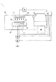
図1〜4は、本発明の実施形態に係るプラズマ処理システムを示す。図1は、本発明の一実施例に係るプラズマ処理システムを示す。プラズマ処理システム1は、基板25を支持するための基板ホルダ20をマウントするための台5を有する処理チャンバ10と、処理チャンバ10にプロセスガス15を導入するガス注入システム40と、チャンバモニタリングシステム100と、真空排気システム50とを具備する。チャンバモニタリングシステム100は、例えば、処理チャンバ10のプラズマからの光発光をモニタリングするための光学的モニタリングシステム、処理チャンバ10のパーティクルレベルをモニタリングするためのパーティクルモニタリングシステム、または処理チャンバ10のガスの環境をモニタリングするためのマスセンサであり得る。
1 to 4 show a plasma processing system according to an embodiment of the present invention. FIG. 1 shows a plasma processing system according to an embodiment of the present invention. The
プロセスガス15は、例えば、マイクロエレクトロニクス素子が形成される製造工程における基板25のエッチングを行うための、またはプラズマドライクリーニングプロセスの処理チャンバ10からチャンバ残渣を除去するためのハロゲン含有、および、カーボン含有エッチングガスであり得る。本発明に係るチャンバ残渣を除去するためのプロセスガスは、カーボンおよび酸素を含むガスを含んでいることができる。ガス注入システム40は、ex―situガス供給源から処理チャンバ10までプロセスガス15の送出の独立した制御を可能にする。プロセスガス15は、ガス注入プレナム(図示せず)、一連のバッフル板(図示せず)、および、マルチオリフィスシャワーヘッドガス注入プレート65を介してプロセス領域60に導入されることができ、処理チャンバの圧力調整され得る。例えば、コントローラ55が、真空排気システム50およびガス注入システム40の制御に用いられる。
The
基板25は、ロボット基板移送システムを介してスロットバルブ、および、チャンバフィードスルーを通ってチャンバ10との間で移送され、基板ホルダ20内に収容された基板リフトピンによって受けられ、そして、収容されているデバイスによって、機械的に移動される。一旦、基板25が基板移送システムから受けられると、それは基板ホルダ20の上面まで降ろされる。基板25は、例えば、シリコン(Si)および化合物半導体(例えばガリウム砒素)のような半導体基板、液晶ディスプレイ(LCD)基板、ガラス製基板、および窒化シリコン(SiN)、炭化珪素(SiC)、およびアルミナ(Al2O3)のようなセラミック材料を含むことができる。、プラズマ処理システム1は、さまざまなサイズの基板、例えば200mm基板、300mm基板、またはより大きい基板の処理を行うように構成されることができる。
The
基板25は、静電クランプまたは機械的なクランプを介して基板ホルダ20に固定されることができる。さらにまた、基板ホルダ20は、基板ホルダ20から熱を受け、および、熱交換器システムに熱を移送する再循環クーラント流量を含んでいる冷却システムを更に含むことができる。代わりとして、基板ホルダ20は、熱交換器システムから基板ホルダ20まで熱を供給する再循環している流体流動を含むことができる。さらに、ガスは、基板25と、基板ホルダ20との間のガスギャップ熱伝導を改良するために、基板の裏面に供給されることができる。基板の温度コントロールが上昇するか低下された温度で必要なときに、このようなシステムは利用される。
The
基板ホルダ20は、加熱部材30を含むことができる。加熱部材30は、例えば、抵抗加熱部材であり得る。真空ポンプシステム50は、1秒あたり5,000リットル(および、より高い)までの排気速度が可能なターボ分子真空ポンプ(TMP)、および、チャンバ圧力を抑えるためのゲートバルブを含むことができる。TMPは、低圧プロセス(一般的に800mTorr未満の)に対して有効である。高圧プロセス(すなわち約800mTorrを超える)に対して、メカニカルブースターポンプ、および、ドライ荒引きポンプが、用いられることができる。
The
プラズマ処理システム1は、処理チャンバ10内にプラズマを形成し、および、維持することが可能である。プラズマ処理システム1は、例えば、プラズマ増強化学蒸着プロセス(plasma enhanced chemical vapor deposition process:PECVD)またはプラズマエッチングプロセスを実行するために利用されることができる。基板ホルダ20は、更に、ラジオ周波数(RF)パワーが通ってプロセス領域60のプラズマに結合される電極としての機能を果たすことができる。例えば、基板ホルダ20の金属電極は、基板ホルダ20にRF発振器45からインピーダンスマッチングネットワーク35を介してRF電力の伝達を通じて、RF電圧で電気的にバイアスをかけられることができる。RFバイアスは、電子を励起し、これにより、プラズマを形成し、維持するために役立つ。この構成において、プラズマは、基板25に材料を堆積させる(すなわち、処理システム1は、PECVDリアクタの働きをすることができる)、または基板25の露出表面から材料を除去する(すなわち、処理システム1は、リアクティブイオンエッチング(RIE)リアクタの働きをすることができる)ことのどちらかに利用される。RFバイアスのための典型的な周波数は、約0.5MHzと、約200MHzとの間であり得て、および、2MHzであり得る。
The
インピーダンスマッチングネットワーク35は、反射パワーを最小にすることによって処理チャンバ10のプラズマにRF電力の伝送を最大にするために役に立つ。マッチングネットワークトポロジ(例えばL−タイプ、π−タイプ、T−タイプ)および自動制御方法は、従来技術において周知である。代わりの実施形態では、RF電力は、複数の周波数で基板ホルダ20に印加されることができる。
The impedance matching
図1において、コントローラ55は、マイクロプロセッサと、メモリと、プラズマ処理システム1と通信し、プラズマ処理システム1への入力をアクティブにし、同じくプラズマ処理システム1からの出力をモニタするために十分な制御電圧を生成することが可能なデジタルI/Oポートとを含む。さらにまた、コントローラ55は、処理チャンバ10、RF発振器45、インピーダンスマッチングネットワーク35、ガス注入システム40、チャンバモニタリングシステム100、および真空ポンプシステム50に組み合わせられ、並びに、それらと情報を交換する。例えば、メモリに格納されたプログラムは、保存されたプロセスレシピに係る処理システム1の前述のコンポーネントの制御に利用されることができる。コントローラ55の1つの実施例は、デジタル信号処理装置(DSP);テキサスインスツルメンツ、ダラス、テキサスから入手可能なモデル番号TMS320である。
In FIG. 1, a
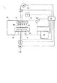
図2は、本発明の一実施例に係るプラズマ処理システムを示す。図2のプラズマ処理システム1は、図1に関して記載したそれらのコンポーネントに加えて、潜在的にプラズマ密度を増加させ、および/またはプラズマ処理均一性を改良するために、機械的にまたは電気的に回転させるDC磁界システム70を更に含む。さらに、コントローラ55は、回転速度、および、磁界の強さを調整するために、回転磁界システム70に組み合わせられる。
FIG. 2 shows a plasma processing system according to one embodiment of the present invention. The
図3は、本発明の一実施例に係るプラズマ処理システムを示す。図3のプラズマ処理システム1は、また、RF電力がインピーダンスマッチングネットワーク75を介してRF発振器80から結合される上部平面電極としての機能を果たすことができるマルチオリフィスシャワーヘッドガス注入プレート65を含む。上部電極に対するRF電力のアプリケーションのための典型的な周波数は、約10MHzと、約200MHzとの間であり得て、および、60MHzであり得る。加えて、下部電極に対する電力供給のための典型的な周波数は、約0.1MHzと、約30MHzとの間であり得て、および、2MHzであり得る。さらに、コントローラ55は、上部電極65に対するRF電力の印加を制御するために、RF発振器80、および、インピーダンスマッチングネットワーク75に結合される。
FIG. 3 shows a plasma processing system according to one embodiment of the present invention. The
本発明の1つの実施形態では、図3の基板ホルダ20は、電気的に接地されることができる。代わりの実施形態では、直流バイアスが、基板ホルダ20に印加されることができる。さらに他の実施例では、基板ホルダ20は、プラズマ処理システム1から電気的に絶縁されることができ、および、電離気体が接触するときに、浮動電位が基板ホルダ20に、および、基板25に形成されることができる。
In one embodiment of the present invention, the
図4は、本発明の1つの実施形態に係るプラズマ処理システムを示す。図2のプラズマ処理システムが、RF電力がインピーダンスマッチングネットワーク90を介してRF発振器85を通じて結合される誘導コイル95を更に含めるために変更される。RF電力は、プロセス領域60に誘電体窓を介して誘導コイル95から誘導的に結合される。誘導コイル80にRF電力を印加するための典型的な周波数は、約10MHzと、約100MHzとの間であり得て、および、13.56MHzであり得る。同様に、基板ホルダ20に対する電力供給のための典型的な周波数は、約0.1MHzと、約30MHzとのの間であり得て、および、13.56MHzであり得る。加えて、スロット付きファラデーシールドは、誘導コイル95と、プラズマとの間の容量結合を減らすために使用されることができる。さらに、コントローラ55は、誘導コイル95に対する電力供給を制御するために、RF発振器85、および、インピーダンスマッチングネットワーク90に結合される。
FIG. 4 illustrates a plasma processing system according to one embodiment of the present invention. The plasma processing system of FIG. 2 is modified to further include an
本発明の1つの実施形態では、図4の基板ホルダ20は、電気的に接地されることができる。代わりの実施形態では、直流バイアスが、基板ホルダ20に印加されることができる。さらに他の実施例では、基板ホルダ20はプラズマ処理システム1から電気的に絶縁されることができ、電離気体が接触するときに、浮動電位が基板ホルダ20に、および、基板25に形成されることができる。
In one embodiment of the present invention, the
本発明の他の実施例において、プラズマは、電子サイクロトロン共鳴(ECR)を使用して形成される。さらに別の実施形態では、プラズマは、ヘリコン波のラウンチングから形成される。さらに他の実施例では、プラズマは、伝搬性表面波から形成される。 In another embodiment of the invention, the plasma is formed using electron cyclotron resonance (ECR). In yet another embodiment, the plasma is formed from helicon wave launching. In yet another embodiment, the plasma is formed from a propagating surface wave.
図1〜図4のプラズマ処理システムが典型的な用途だけのためにあると理解されることになっており、特定のハードウェアおよびソフトウェアの多くの変化が本発明が実施されることができるシステムを実施するために用いることができるとき、これらの変化は、当業者に直ちに明らかである。 It is to be understood that the plasma processing system of FIGS. 1-4 is for typical applications only, and many variations of specific hardware and software can be implemented in the present invention. These changes will be readily apparent to those skilled in the art.
上記のように、従来のドライクリーニングプロセスは、チャンバ内部から残渣を除去することに効果的であるとは限られず、一般に、ドライクリーニングプロセスの基板ホルダへのダメージを防ぐためにシールド基板の使用することを必要とする。本発明の発明者は、処理チャンバからクリーニング残渣に効果的であるドライクリーニングプロセスを見いだした。そして、プロセスがシールド基板なしで実行されることができるために、いままでより基板ホルダに害とはならなかった。シールド基板のないドライクリーニングを実行するこの能力は、静電チャックタイプ基板ホルダの改良された動作を提供することができる基板ホルダのより効果的クリーニングを可能とする。本発明のドライクリーニングプロセスは、図1〜図4に関して記載されているプラズマ処理システムのどれにでもクリーニングするのに使われることができる。 As noted above, conventional dry cleaning processes are not always effective at removing residues from the interior of the chamber and generally use shield substrates to prevent damage to the substrate holder in the dry cleaning process. Need. The inventors of the present invention have found a dry cleaning process that is effective on cleaning residues from the processing chamber. And since the process can be carried out without a shield substrate, it has never been more harmful to the substrate holder. This ability to perform dry cleaning without a shield substrate allows for more effective cleaning of the substrate holder, which can provide improved operation of the electrostatic chuck type substrate holder. The dry cleaning process of the present invention can be used to clean any of the plasma processing systems described with respect to FIGS.
本発明の一実施態様において、方法は、プラズマ、並びに、カーボンおよび酸素を含むガスを含んでいるプロセスガスを利用して、プラズマ処理システムからチャンバ残渣を除去するために提供される。ドライクリーニングプロセスは、少なくとも1枚の生産基板(ウェハ)をプロセスした後に実行され得て、ドライクリーニングプロセスは、基板ホルダ(ウェーハチャック)上の基板なしで実行されることができる。これはウェハのないドライクリーニング(waferless dry cleaning:WDC)プロセスと呼ばれる。WDCプロセスは、基板ホルダ、同じく他のチャンバコンポーネント、および、チャンバ壁から残渣を効果的に除去することができる。さらに、WDCプロセスを利用するときに、クリーニングプロセスの間のウェハロードおよびアンロード時間がないことは、クリーニング時間を減らすことができ、および、製造スループットを増加させることができる。(非生産品)基板が、更に以下に記載されるように、プラズマ環境から基板ホルダを保護するために、ドライクリーニングプロセスの間、基板ホルダに存在することができるときでも、本発明は、また従来のドライクリーニングプロセスを超えた改良されたチャンバクリーニングを提供する。 In one embodiment of the present invention, a method is provided for removing chamber residues from a plasma processing system utilizing a plasma and a process gas comprising a gas comprising carbon and oxygen. The dry cleaning process can be performed after processing at least one production substrate (wafer), and the dry cleaning process can be performed without a substrate on a substrate holder (wafer chuck). This is called a waferless dry cleaning (WDC) process. The WDC process can effectively remove residues from the substrate holder, as well as other chamber components and chamber walls. Furthermore, the absence of wafer load and unload time during the cleaning process when utilizing the WDC process can reduce cleaning time and increase manufacturing throughput. Even when the (non-product) substrate can be present in the substrate holder during the dry cleaning process to protect the substrate holder from the plasma environment, as described further below, the present invention also It provides improved chamber cleaning over conventional dry cleaning processes.
本発明に係るドライクリーニングプロセスは、処理チャンバ内で、各々の製造工程の後で実行されることができ、または、代わりとして、複数の製造工程の後で実行される。ドライクリーニングプロセスの後、次の製造基板が処理チャンバへ移送され、そして、処理されるときに、以前の製造基板がされたのと同様のチャンバ条件と基板が向かい合うことができる。したがって、基板に対する基板変動は、最小にされることができる。 The dry cleaning process according to the present invention can be performed after each manufacturing step in the processing chamber, or alternatively after a plurality of manufacturing steps. After the dry cleaning process, the next manufacturing substrate is transferred to the processing chamber, and when processed, the substrate can face the same chamber conditions as the previous manufacturing substrate was done. Accordingly, substrate variation relative to the substrate can be minimized.
カーボンおよび酸素を含んでいるガスは、一酸化炭素(CO)、二酸化炭素(CO2)、アルコール(ROH)、アルデヒド(RCHO)、および、ケトン(R1COR2)。を含む多種多様なガスから選ばれることができる。アルコールは、線形の炭素鎖、例えば、メタノール(CH3OH)、エタノール(CH3CH2OH)、プロパノール(CH3CH2CH2OH)、および、分岐炭素鎖、例えば2―プロパノール((CH3)2CHOH)、および、テトラ―ブチルアルコール((CH3)3COH)を含むことができる。プロセスガスは、水素(H2)、アンモニア(NH3)、水(H2O)、窒素(N2)、および、アルゴン(Ar)、ヘリウム(He)またはキセノン(Xe)のような不活性ガスのうちの少なくとも1つを更に含むことができる。ここで使用しているように語「a,b、c...またはxの少なくとも1つ」は、記載されたエレメントのどの1つでも、または複数の記載されたエレメントの何らかの組合せのどれでも参照する。 The gas containing carbon and oxygen is carbon monoxide (CO), carbon dioxide (CO 2 ), alcohol (ROH), aldehyde (RCHO), and ketone (R 1 COR 2 ). Can be selected from a wide variety of gases. Alcohols are linear carbon chains such as methanol (CH 3 OH), ethanol (CH 3 CH 2 OH), propanol (CH 3 CH 2 CH 2 OH), and branched carbon chains such as 2-propanol ((CH 3 ) 2 CHOH), and tetra-butyl alcohol ((CH 3 ) 3 COH). Process gases are hydrogen (H 2 ), ammonia (NH 3 ), water (H 2 O), nitrogen (N 2 ), and inert such as argon (Ar), helium (He) or xenon (Xe) At least one of the gases can further be included. As used herein, the term “at least one of a, b, c... Or x” can be any one of the described elements or any combination of a plurality of described elements. refer.
本発明の一実施例に係るドライクリーニングプロセスは、クリーンなチャンバをもたらすと判っている所定の時間の間、実行され得て、または、代わりとして、ドライクリーニングプロセスの終点は終点検出方法を使用して決定されることができる。この点に関しては、クリーン度の許容可能なレベルは、処理チャンバ内で実行される製造工程に従って変化するものであると理解される。終点検出の1つの可能な方法は、プラズマ領域からの放出光スペクトルの一部をモニタする光学的モニタリングシステムを使用することであり、それは、ドライクリーニングプロセスの状態に関する情報を、それによって提供され、チャンバ残渣の全て(または実質的に全て)が処理チャンバから除去されたときかどうかを示す。 The dry cleaning process according to one embodiment of the present invention can be performed for a predetermined time known to result in a clean chamber, or alternatively, the end point of the dry cleaning process uses an end point detection method. Can be determined. In this regard, it is understood that the acceptable level of cleanliness will vary according to the manufacturing process performed in the processing chamber. One possible method of endpoint detection is to use an optical monitoring system that monitors a portion of the emitted light spectrum from the plasma region, which provides information about the status of the dry cleaning process, Indicates whether all (or substantially all) of the chamber residue has been removed from the processing chamber.
例えば、スペクトルの一部である、482.5nm(一酸化炭素、CO)、775.5nm(弗素、F)、および、440nm(四フッ化ケイ素、SiF4)の波長をもって、このような除去を示し、および、光学発光分光法(OES)を使用して測定されることができる。775.5nmの弗素発光は、プラズマ環境中の(すなわち弗素メモリー効果)、および、処理チャンバの弗素を含有するチャンバ残渣の量を、弗素ラジカルの相対的な量として示す。482.5nmの一酸化炭素発光は、処理チャンバのチャンバコンポーネント、および、他の表面からの高分子残渣の離脱に関連があることがあり得る。それらの周波数に対応する発光レベルが指定された閾値(例えば、実質的にゼロに落ちるかまたは特定のレベル以下まで減少する)を横切ったあと、ドライクリーニングプロセスは完了すると考えられることができる。 For example, such removal is possible with wavelengths of 482.5 nm (carbon monoxide, CO), 775.5 nm (fluorine, F), and 440 nm (silicon tetrafluoride, SiF 4 ) that are part of the spectrum. Can be measured and measured using optical emission spectroscopy (OES). The 775.5 nm fluorine emission indicates the amount of chamber residue in the plasma environment (ie, fluorine memory effect) and containing fluorine in the processing chamber as a relative amount of fluorine radicals. The 482.5 nm carbon monoxide emission can be related to the removal of polymer residues from the chamber components of the processing chamber and other surfaces. After the emission levels corresponding to those frequencies cross a specified threshold (eg, substantially drop to zero or decrease below a certain level), the dry cleaning process can be considered complete.
終点検出の別の方法は、処理チャンバのガスの環境をモニタするためのマスセンサを使用することを含む。終点検出のさらに別の方法は、プラズマ処理システムの作動パラメータをモニタすることであって、それは、RF発振器ピーク間電圧、および、インピーダンスマッチングネットワークにおけるコンデンサポジションを含む。終点検出のさらにもう一つの方法は、パーティクルモニタリングシステムを使用して処理チャンバのパーティクルレベルをモニタすることである。 Another method of endpoint detection involves using a mass sensor to monitor the gas environment of the processing chamber. Yet another method of endpoint detection is to monitor the operating parameters of the plasma processing system, which includes the RF oscillator peak-to-peak voltage and the capacitor position in the impedance matching network. Yet another method of endpoint detection is to monitor the particle level in the processing chamber using a particle monitoring system.
図5〜図7は、本発明の実施形態に係る、プラズマ処理システムの実行しているWDCプロセスからの光発光の変化を示す。これらの図は、チャンバ内部から残渣を除去する際の本発明の効果を示す。図5〜図7のデータを生成するために使用するプラズマ処理システムは、上記の図3に概略的に示される。プラズマ条件は、100mTorrのチャンバ圧力、60MHzの750Wの上部電極RF電力、および2MHzの250Wの下部電極RF電力を含んでいた。プラズマ発光は、異なるプロセスガス、および、プロセスガス混合物に対するWDCプロセスを評価するために、プロセス領域からモニタされた。、図5〜図7の各々のカーブは、チャンバの初期の光発光測定と、エッチングおよびドライクリーニングプロセスの3サイクルが実行されたあとにとられた光発光測定との間の違いを示す。具体的には、Ar+O2プロセスガス(基板ホルダ上のクリーンなSiウェハがある場合)を含んでいるプラズマから、初期の光発光は、3分のOES走査を使用して検出された。それで、次の処理手順は、3回実行された:a)基板ホルダ上のSi基板(ウェハ)がある場合には、low−k材料または平坦化材料のために開発されたプラズマエッチングプロセスを実行すること、b)30秒のWDCプラズマプロセスを実行すること。プラズマエッチングプロセスは、チャンバ内部に堆積しているチャンバ残渣をもたらす。それで、エッチング、および、クリーニングサイクルの後、チャンバの残渣の量を決定するためにAr+O2プロセスガス(基板ホルダ上のクリーンなSiウェハがある場合)を含んでいるプラズマから、別の光発光測定は、3分のOES走査を使用して検出された。図5〜図7において各々の5つのカーブとして、初期測定と、後処理測定との間の違いは、示される。これらのカーブの水平軸は、3分のOES走査を表す。 5-7 illustrate changes in light emission from a WDC process performed by a plasma processing system, according to an embodiment of the present invention. These figures show the effect of the present invention in removing residue from the interior of the chamber. The plasma processing system used to generate the data of FIGS. 5-7 is schematically illustrated in FIG. 3 above. The plasma conditions included a chamber pressure of 100 mTorr, a 750 W upper electrode RF power at 60 MHz, and a 250 W lower electrode RF power at 2 MHz. Plasma emission was monitored from the process area to evaluate WDC processes for different process gases and process gas mixtures. Each curve in FIGS. 5-7 shows the difference between the initial light emission measurement of the chamber and the light emission measurement taken after three cycles of the etching and dry cleaning processes have been performed. Specifically, initial light emission was detected using a 3 minute OES scan from a plasma containing Ar + O 2 process gas (if there is a clean Si wafer on the substrate holder). So the following procedure was performed three times: a) If there is a Si substrate (wafer) on the substrate holder, perform the plasma etching process developed for low-k material or planarization material B) performing a 30 second WDC plasma process. The plasma etch process results in chamber residues that are deposited inside the chamber. So after etching and cleaning cycles, another photoluminescence measurement from the plasma containing Ar + O 2 process gas (if there is a clean Si wafer on the substrate holder) to determine the amount of chamber residue Was detected using a 3 minute OES scan. The difference between the initial measurement and the post-processing measurement is shown as each of the five curves in FIGS. The horizontal axis of these curves represents a 3 minute OES scan.
図5は、本発明の実施形態に係る775.5nmで弗素信号の変化を示す。図5のカーブは、毎分標準状態での500立方センチメートルの一酸化炭素ガス流量(sccm)、および、0sccmのArガス流量、250sccm、500sccm、および、1000sccmを使用してWDCプロセスに対応する。750sccmのArガス流量、および、750sccmのO2ガス流量を有するAr+O2プラズマクリーニングプロセスを利用してWDCプロセスは、また、示される。図5の結果は、純粋なCOガスまたはCO+Arガスを利用したWDCプロセスが、従来のAr+O2ドライクリーニングプラズマプロセスと比較した場合に、減少された弗素信号を示し、したがって、処理チャンバ内のチャンバ堆積物は、減少された。ArがCOとともに用いられるときに、一酸化炭素、および、Arの等しいガス流れ(それぞれ500sccm)は、最も低い弗素信号をもたらした。
FIG. 5 shows the change in fluorine signal at 775.5 nm according to an embodiment of the present invention. The curves in FIG. 5 correspond to a WDC process using 500 cubic centimeters of carbon monoxide gas flow (sccm) at standard conditions per minute and an Ar gas flow of 0 sccm, 250 sccm, 500 sccm, and 1000 sccm. A WDC process utilizing an Ar + O 2 plasma cleaning process with an Ar gas flow rate of 750 sccm and an O 2 gas flow rate of 750 sccm is also shown. The results of FIG. 5 show a reduced fluorine signal when a WDC process utilizing pure CO gas or CO + Ar gas is compared to a conventional Ar +
図6は、本発明の実施形態に係る775.5nmでの弗素信号の変化を示す。図6のカーブは、500sccmのCOガス流量および0sccm、250sccm、500sccm、および、750sccmのO2ガス流量を利用したWDCプロセスに対応する。図6の結果は、何らかの付加的なO2のない純粋な一酸化炭素を利用して100mTorrのチャンバ圧力のWDCプロセスが処理チャンバの弗素信号を減らすことに最も効果的だったことを示す。図6は、600mTorrのチャンバ圧力で実行され、500sccmのCOガス流量、および、750sccmのO2ガス流量を利用したWDCプロセスを示し、100mTorrのチャンバ圧力で純粋なCOとして同様の弗素信号を得られたことを示す。さらにまた、図6の結果は、弗素信号の減少がO2ガス流量の線形関数でなかったことを示す。 FIG. 6 shows the change in fluorine signal at 775.5 nm according to an embodiment of the present invention. The curve in FIG. 6 corresponds to a WDC process utilizing a CO gas flow rate of 500 sccm and O 2 gas flow rates of 0 sccm, 250 sccm, 500 sccm, and 750 sccm. The results in FIG. 6 show that a 100 mTorr chamber pressure WDC process was most effective at reducing the fluorine signal in the processing chamber utilizing pure carbon monoxide without any additional O 2 . FIG. 6 shows a WDC process performed at a chamber pressure of 600 mTorr and using a CO gas flow rate of 500 sccm and an O 2 gas flow rate of 750 sccm, and a similar fluorine signal can be obtained as pure CO at a chamber pressure of 100 mTorr. It shows that. Furthermore, the results of FIG. 6 show that the decrease in fluorine signal was not a linear function of O 2 gas flow rate.
図7は、本発明の実施形態に係る482.5nmでCO信号の変化を示す。図7の結果は、純粋なCOガスを利用したWDCプロセスが従来のAr+O2ドライクリーニングプラズマプロセスと同等であるCO発光を得ることを示す。さらにまた、図7は、WDCプロセス(放電でない)を実行しない影響、および、純粋なH2ガスを用いたWDCプロセスを実行する影響を示す。 FIG. 7 shows the change in the CO signal at 482.5 nm according to an embodiment of the present invention. The results in FIG. 7 show that the WDC process using pure CO gas obtains CO emission that is equivalent to the conventional Ar + O 2 dry cleaning plasma process. Furthermore, FIG. 7 shows the effect of not performing the WDC process (not discharging) and the effect of performing the WDC process with pure H 2 gas.
本発明に係るドライクリーニングプロセスのためのプロセスパラメータ空間は、例えば、約10mTorrと、約5Torrとの間のチャンバ圧力を利用することができる。本発明の別の実施形態では、チャンバ圧力は、約20mTorrと、約1Torrとの間であり得て、および、約100のmTorrであり得る。図3の上下の電極へのRF電力に対する典型的な周波数は、約1MHzと、約100MHzとの間であり得る。例えば、上部電極RF電力は、約100Wと、約4,000Wとの間であり得て、好ましくは60MHzの約750Wである。さらにまた、下部電極RF電力は、約0Wと、約4,000Wとの間であり得て、2MHzの約250Wであり得る。約100sccmと、約5,000sccmとの間のプロセスガス流量が使われることができる。さらにまた、約100sccmと、約2,000sccmとの間のガス流量が、カーボンおよび酸素を含むガスに対して使われることができ、約20sccmと、約1,000sccmと間のガス流量が、H2、H2O、NH3、および、N2に対して使われることができ、および、約2,000sccm未満のガス流量が、不活性ガスに対して使われることができる。 The process parameter space for the dry cleaning process according to the present invention can utilize, for example, a chamber pressure between about 10 mTorr and about 5 Torr. In another embodiment of the invention, the chamber pressure can be between about 20 mTorr and about 1 Torr, and can be about 100 mTorr. A typical frequency for RF power to the upper and lower electrodes of FIG. 3 can be between about 1 MHz and about 100 MHz. For example, the top electrode RF power can be between about 100 W and about 4,000 W, preferably about 750 W at 60 MHz. Furthermore, the lower electrode RF power can be between about 0 W and about 4,000 W, and can be about 250 W at 2 MHz. Process gas flow rates between about 100 sccm and about 5,000 sccm can be used. Furthermore, a gas flow rate between about 100 sccm and about 2,000 sccm can be used for a gas containing carbon and oxygen, and a gas flow rate between about 20 sccm and about 1,000 sccm is H 2 , H 2 O, NH 3 , and N 2 can be used, and gas flow rates of less than about 2,000 sccm can be used for inert gases.
さらにまた、チャンバ圧力、および、プロセスガスの組成は、プラズマクリーニングプロセスの間、変化されることができる。プラズマクリーニングのための時間期間は、実質的に処理チャンバのフルオロカーボンチャンバ残渣の量を減らすために、十分に長くされるべきである。クリーニングプロセスのための時間期間は、例えば、約2秒と、約240秒との間であり得る。代わりとして、時間期間は、約15秒と、約40秒との間であり得る。 Furthermore, the chamber pressure and the composition of the process gas can be changed during the plasma cleaning process. The time period for plasma cleaning should be sufficiently long to substantially reduce the amount of fluorocarbon chamber residue in the processing chamber. The time period for the cleaning process can be, for example, between about 2 seconds and about 240 seconds. Alternatively, the time period can be between about 15 seconds and about 40 seconds.
図8は、本発明の実施形態に係るプラズマ処理システムの処理チャンバからチャンバ残渣を除去する方法を示しているフローチャートである。802で、クリーニングプロセス800は、始まった。804で、カーボンおよび酸素を含むガスを含んでいるプロセスガスは、プラズマ処理システムの処理チャンバ内に導入される。806で、プラズマは、プロセスガスから生成される。808で、チャンバ残渣は、揮発性の反応生成物を形成するように、ドライ洗浄工程のプラズマに曝される。810で、反応生成物は、処理システムから排気され、そして、812で、プロセスはストップされる。
FIG. 8 is a flowchart illustrating a method for removing chamber residues from a processing chamber of a plasma processing system according to an embodiment of the present invention. At 802, the
図9は、本発明の実施形態に係るプラズマ処理システムのモニタリング、および、制御する方法を示しているフローチャートである。プロセス900は、上記のドライクリーニングプロセス800のモニタリング、および、制御である得る。902で、プロセスは、始まられる。904で、プラズマ処理システムは、チャンバモニタリングシステムによってモニタされる。モニタリングは、例えば、プロセス環境、クリーニングガス、および/または揮発性の反応生成物からのマス信号、パーティクルレベル、またはプロセスパラメータのガスからの発光信号または光吸収信号に基づくことがあり得る。クリーニングプロセスの間、チャンバ残渣は、処理チャンバ(処理チャンバ内のチャンバコンポーネント、および、他の表面からを含む)から除去される。プロセスが処理チャンバ内の継続するときに、これは、モニタされた信号を変更することができる。信号のこの変化は、モニタリングシステムによって検出されることができ、および、処理チャンバの状態と相関していることができる。906で、もし検出信号強度が閾値に到達しなかったならば、プロセス900は904で継続され、または、もし906で信号が閾値に到達したならば、決定は908においてされ、プロセス800を続けるか、または910のプロセスをストップするかがされる。
FIG. 9 is a flowchart illustrating a method for monitoring and controlling a plasma processing system according to an embodiment of the present invention.
信号強度は、クリーニングプロセスの終点を決定するためにモニタされることができる。ドライクリーニングプロセスの終点に対する信号強度の相関は、信号強度を検出し、処理チャンバの状態をモニタリングする間に実行されるテストプロセスによって、実施されることができる。処理チャンバの状態は、例えば、テストプロセスの間、チャンバコンポーネントを検査し、および、検査された結果をドライクリーニングプロセスの所望の終点が観測されるときに、強度が記録された検出閾値に関連させることによって評価されることができる。閾値は、強度が固定された強度値、または測定された信号強度と、初期の信号強度(プロセスの開始時に測定された)との比率であることができる。 The signal strength can be monitored to determine the end point of the cleaning process. The correlation of signal strength to the end point of the dry cleaning process can be performed by a test process performed while detecting the signal strength and monitoring the condition of the processing chamber. The state of the processing chamber, for example, inspects the chamber components during the test process, and relates the inspected result to a detection threshold at which the intensity is recorded when the desired end point of the dry cleaning process is observed. Can be evaluated by The threshold value can be an intensity value with a fixed intensity or a ratio of the measured signal intensity to the initial signal intensity (measured at the start of the process).
図10は、本発明の実施形態に係るプラズマ処理システムのモニタリング状態のための処理時間の関数としてのグラフを示している信号強度である。信号は、例えば、発光信号(例えば482.5nmの弗素信号、775.5nmのCO信号または440nmの四フッ化ケイ素信号)、クリーニングガス、および/または反応生成物(例えばSiF4)からのマス信号、プラズマパラメータ、またはパーティクルレベルであり得る。カーブ1070によって示されるように、処理チャンバからチャンバ残渣の除去、および、処理チャンバのチャンバ残渣の減少する量のために、ドライクリーニングプロセスが行われるとき、検出信号強度は一般に減少する。図10のカーブ1070が信号強度の実質的な線形の減少を示すのに対して、信号強度カーブがクリーニングプロセスの特性に依存し、および、非線形であることができると理解される。また、図10に示すとき、チャンバコンポーネントが所望のプロセスのための許容できるクリーンなレベルにあると判るときに、閾値強度1080は時間1090にて検出される。許容できるクリーンなレベルがチャンバにおいて実行される工程に従い変化することができると理解される。
FIG. 10 is a signal intensity showing a graph as a function of processing time for a monitoring state of a plasma processing system according to an embodiment of the present invention. The signals may be, for example, emission signals (eg, 482.5 nm fluorine signal, 775.5 nm CO signal or 440 nm silicon tetrafluoride signal), cleaning gases, and / or mass signals from reaction products (eg, SiF 4 ). , Plasma parameters, or particle level. As indicated by
図9に一旦戻って、信号強度がドライクリーニングプロセスの間、904で検出されるとき、コントローラは、検出信号強度を従来の保存された信号強度と906で比較し、そして、検出信号強度が所定の閾値強度に到達したかどうかを決定する。信号閾値強度がまだ検出されないときに、モニタリングは904に戻り、そして、プロセスは継続する。閾値信号強度が検出されるときに、決定は、904でのプロセスを続けるべきであるか、または908でのプロセスを止めるべきか908においてなされる。代わりとして、908でのプロセスを続けるかの決定は、プロセスの第2のフェーズを入力するためにプロセスパラメータの調整を含むことができ、第2の閾値が到達されるまで、それは、モニタされる。例えば、温度および/またはクリーニングガス濃度は、よりゆるやかなクリーニング環境に影響するまで低下させた。 Returning to FIG. 9, when the signal strength is detected at 904 during the dry cleaning process, the controller compares the detected signal strength with the conventional stored signal strength at 906 and the detected signal strength is predetermined. Determine if the threshold strength of is reached. When the signal threshold strength is not yet detected, monitoring returns to 904 and the process continues. When a threshold signal strength is detected, a decision should be made at 908 whether to continue the process at 904 or stop the process at 908. Alternatively, the decision to continue the process at 908 can include adjustment of process parameters to enter the second phase of the process, which is monitored until a second threshold is reached. . For example, the temperature and / or cleaning gas concentration was reduced until it affected a more gradual cleaning environment.
本発明の多数の修正変更は、上記の教示を考慮して可能である。それは、従って、添付の請求の範囲で、ここで特に記載されているより、別な方法で本発明が実施されることができると理解されるものである。 Many modifications and variations of the present invention are possible in light of the above teachings. It is therefore to be understood that within the scope of the appended claims, the invention may be practiced otherwise than as specifically described herein.
Claims (24)
プラズマ処理システムの処理チャンバに、CO、CO2、またはこれらの分子の少なくとも1つとH2,NH3、H2O、N2、若しくは不活性ガスの1つ以上との組み合わせからなるプロセスガスを導入することと;
前記プロセスガスからプラズマを生成することと;
前記残渣から揮発性の反応生成物を形成するために、前記フルオロカーボン高分子チャンバ残渣を、基板ホルダがウェハのないドライクリーニングプロセスによってクリーニングされるように前記プラズマ処理システムの前記基板ホルダにシールドウェハが提供されていない前記ウェハのないドライクリーニングプロセスの前記プラズマにさらすことと;
前記処理チャンバから前記反応生成物を排気することとを具備する方法。A method for removing fluorocarbon polymer chamber residues from a plasma processing system comprising:
A processing chamber of a plasma processing system, a combination of a CO, CO 2, also FUN least one of H 2 these molecules, NH 3, H 2 O, N 2, or one or more inert gases Introducing process gas;
Generating a plasma from the process gas;
In order to form a volatile reaction product from the residue, the fluorocarbon polymer chamber residue is removed from the substrate holder of the plasma processing system so that the substrate holder is cleaned by a dry cleaning process without the wafer. Exposing the plasma to a dry cleaning process without the wafer being provided;
Evacuating the reaction product from the processing chamber.
前記生成することは、前記電極へ、1MHzから100MHzまでの間のRF周波数、および100Wから4,000Wまでの間のRF電力を印加することを備えている請求項1に記載の方法。The plasma processing system includes an upper electrode and a lower electrode,
The method of claim 1, wherein the generating comprises applying an RF frequency between 1 MHz and 100 MHz and RF power between 100 W and 4,000 W to the electrode.
前記上部電極に印加される前記RF電力は、600Wから900Wまでの間であり、
前記下部電極に印加される前記RF周波数は、1MHzから3MHzまでの間であり、
前記下部電極に印加される前記RF電力は、100Wから400Wまでの間である請求項11に記載の方法。The RF frequency applied to the upper electrode is between 40 MHz and 80 MHz;
The RF power applied to the upper electrode is between 600W and 900W;
The RF frequency applied to the lower electrode is between 1 MHz and 3 MHz;
The method of claim 11, wherein the RF power applied to the lower electrode is between 100 W and 400 W.
前記信号に基づき、次の1つを実行することとを更に具備する請求項1に記載の方法。
(a)前記ドライクリーニングプロセスを実行することを継続し、モニタリングすることを継続する。
または
(b)前記クリーニングプロセスをストップさせる。Monitoring a signal representative of the progress of the dry cleaning method from the plasma processing system;
The method of claim 1, further comprising performing one of the following based on the signal.
(A) Continue to perform the dry cleaning process and continue to monitor.
Or (b) stopping the cleaning process.
Applications Claiming Priority (3)
| Application Number | Priority Date | Filing Date | Title |
|---|---|---|---|
| US10/813,390 | 2004-03-31 | ||
| US10/813,390 US7959970B2 (en) | 2004-03-31 | 2004-03-31 | System and method of removing chamber residues from a plasma processing system in a dry cleaning process |
| PCT/US2005/002689 WO2005102545A2 (en) | 2004-03-31 | 2005-01-28 | System and method of removing chamber residues from a plasma processing system in a dry cleaning process |
Publications (3)
| Publication Number | Publication Date |
|---|---|
| JP2007531996A JP2007531996A (en) | 2007-11-08 |
| JP2007531996A5 JP2007531996A5 (en) | 2008-05-08 |
| JP4801045B2 true JP4801045B2 (en) | 2011-10-26 |
Family
ID=35059487
Family Applications (1)
| Application Number | Title | Priority Date | Filing Date |
|---|---|---|---|
| JP2007506148A Expired - Fee Related JP4801045B2 (en) | 2004-03-31 | 2005-01-28 | Method for removing chamber residue from a plasma processing system in a dry cleaning process |
Country Status (4)
| Country | Link |
|---|---|
| US (1) | US7959970B2 (en) |
| JP (1) | JP4801045B2 (en) |
| TW (1) | TWI291997B (en) |
| WO (1) | WO2005102545A2 (en) |
Cited By (1)
| Publication number | Priority date | Publication date | Assignee | Title |
|---|---|---|---|---|
| KR20180008409A (en) * | 2015-05-14 | 2018-01-24 | 도쿄엘렉트론가부시키가이샤 | Cleaning method and plasma treatment method |
Families Citing this family (23)
| Publication number | Priority date | Publication date | Assignee | Title |
|---|---|---|---|---|
| JP2002286636A (en) * | 2001-01-19 | 2002-10-03 | Advantest Corp | Chemical substance detecting method and device |
| JP2005033173A (en) * | 2003-06-16 | 2005-02-03 | Renesas Technology Corp | Method for manufacturing semiconductor integrated circuit device |
| KR100605942B1 (en) * | 2004-07-16 | 2006-08-02 | 동부일렉트로닉스 주식회사 | Method for post-treating metal interconnects of semiconductor devices |
| US7862683B2 (en) * | 2005-12-02 | 2011-01-04 | Tokyo Electron Limited | Chamber dry cleaning |
| JP2007287935A (en) * | 2006-04-17 | 2007-11-01 | Toshiba Corp | Vapor phase epitaxy device, and method for manufacturing semiconductor device using it |
| US8292698B1 (en) | 2007-03-30 | 2012-10-23 | Lam Research Corporation | On-line chamber cleaning using dry ice blasting |
| US20100024840A1 (en) * | 2008-07-29 | 2010-02-04 | Chang-Lin Hsieh | Chamber plasma-cleaning process scheme |
| KR101794069B1 (en) * | 2010-05-26 | 2017-12-04 | 삼성전자주식회사 | equipment for manufacturing semiconductor device and seasoning process optimization method of the same |
| DE102011056538A1 (en) * | 2011-12-16 | 2013-06-20 | Aixtron Se | Method for removing unwanted residues of process chamber of chemical vapor deposition reactor, involves forming non-volatile intermediate, so that surface coverage degree of residue is increased/decreased at respective phases of cycle |
| US9048066B2 (en) | 2012-07-03 | 2015-06-02 | Spts Technologies Limited | Method of etching |
| US10724137B2 (en) | 2013-02-05 | 2020-07-28 | Kokusai Eletric Corporation | Cleaning method, method of manufacturing semiconductor device, substrate processing apparatus, recording medium, and cleaning completion determining method |
| US9824865B2 (en) * | 2014-03-05 | 2017-11-21 | Lam Research Corporation | Waferless clean in dielectric etch process |
| US9478390B2 (en) * | 2014-06-30 | 2016-10-25 | Fei Company | Integrated light optics and gas delivery in a charged particle lens |
| JP6638334B2 (en) * | 2015-11-05 | 2020-01-29 | 栗田工業株式会社 | Cleaning method and cleaning device for plasma processing device parts |
| US20170133284A1 (en) * | 2015-11-05 | 2017-05-11 | Texas Instruments Incorporated | Smart in-situ chamber clean |
| JP6638360B2 (en) * | 2015-12-08 | 2020-01-29 | 栗田工業株式会社 | Cleaning method and cleaning apparatus for plasma processing apparatus |
| KR102304823B1 (en) | 2016-03-31 | 2021-09-23 | 도쿄엘렉트론가부시키가이샤 | Controlling Dry Etching Process Characteristics Using Waferless Dry Cleaning Light Emission Spectroscopy |
| US10436717B2 (en) | 2016-11-18 | 2019-10-08 | Tokyo Electron Limited | Compositional optical emission spectroscopy for detection of particle induced arcs in a fabrication process |
| JP2018107264A (en) * | 2016-12-26 | 2018-07-05 | 東京エレクトロン株式会社 | Consumption determining method and plasma processing device |
| US10446453B2 (en) | 2017-03-17 | 2019-10-15 | Tokyo Electron Limited | Surface modification control for etch metric enhancement |
| US10410845B2 (en) | 2017-11-22 | 2019-09-10 | Applied Materials, Inc. | Using bias RF pulsing to effectively clean electrostatic chuck (ESC) |
| JP2020077750A (en) * | 2018-11-07 | 2020-05-21 | 東京エレクトロン株式会社 | Cleaning method and film forming method |
| US12032302B2 (en) | 2021-03-26 | 2024-07-09 | Taiwan Semiconductor Manufacturing Company, Ltd. | Method and device for cleaning substrates |
Citations (3)
| Publication number | Priority date | Publication date | Assignee | Title |
|---|---|---|---|---|
| JP2000195830A (en) * | 1998-12-28 | 2000-07-14 | Mitsubishi Electric Corp | Semiconductor equipment, method for cleaning the same, semiconductor device and its manufacture |
| JP2002289535A (en) * | 2001-03-26 | 2002-10-04 | Seiko Epson Corp | Cleaning method of plasma cvd system |
| JP2003282465A (en) * | 2002-03-26 | 2003-10-03 | Hitachi Ltd | Method of manufacturing semiconductor device |
Family Cites Families (10)
| Publication number | Priority date | Publication date | Assignee | Title |
|---|---|---|---|---|
| US5403434A (en) * | 1994-01-06 | 1995-04-04 | Texas Instruments Incorporated | Low-temperature in-situ dry cleaning process for semiconductor wafer |
| TW394989B (en) * | 1997-10-29 | 2000-06-21 | Matsushita Electronics Corp | Semiconductor device manufacturing and reaction room environment control method for dry etching device |
| US5993679A (en) * | 1997-11-06 | 1999-11-30 | Anelva Corporation | Method of cleaning metallic films built up within thin film deposition apparatus |
| US20020148816A1 (en) * | 2001-04-17 | 2002-10-17 | Jung Chang Bo | Method and apparatus for fabricating printed circuit board using atmospheric pressure capillary discharge plasma shower |
| US6545245B2 (en) * | 2001-05-02 | 2003-04-08 | United Microelectronics Corp. | Method for dry cleaning metal etching chamber |
| JP2004005923A (en) * | 2002-03-29 | 2004-01-08 | Fujitsu Ltd | Method for manufacturing magnetic head, magnetic head and method for forming pattern |
| US20040018715A1 (en) * | 2002-07-25 | 2004-01-29 | Applied Materials, Inc. | Method of cleaning a surface of a material layer |
| US7097716B2 (en) * | 2002-10-17 | 2006-08-29 | Applied Materials, Inc. | Method for performing fluorocarbon chamber cleaning to eliminate fluorine memory effect |
| US7122125B2 (en) * | 2002-11-04 | 2006-10-17 | Applied Materials, Inc. | Controlled polymerization on plasma reactor wall |
| US7041608B2 (en) * | 2004-02-06 | 2006-05-09 | Eastman Kodak Company | Providing fluorocarbon layers on conductive electrodes in making electronic devices such as OLED devices |
-
2004
- 2004-03-31 US US10/813,390 patent/US7959970B2/en not_active Expired - Fee Related
-
2005
- 2005-01-28 JP JP2007506148A patent/JP4801045B2/en not_active Expired - Fee Related
- 2005-01-28 WO PCT/US2005/002689 patent/WO2005102545A2/en active Application Filing
- 2005-03-31 TW TW094110240A patent/TWI291997B/en not_active IP Right Cessation
Patent Citations (3)
| Publication number | Priority date | Publication date | Assignee | Title |
|---|---|---|---|---|
| JP2000195830A (en) * | 1998-12-28 | 2000-07-14 | Mitsubishi Electric Corp | Semiconductor equipment, method for cleaning the same, semiconductor device and its manufacture |
| JP2002289535A (en) * | 2001-03-26 | 2002-10-04 | Seiko Epson Corp | Cleaning method of plasma cvd system |
| JP2003282465A (en) * | 2002-03-26 | 2003-10-03 | Hitachi Ltd | Method of manufacturing semiconductor device |
Cited By (2)
| Publication number | Priority date | Publication date | Assignee | Title |
|---|---|---|---|---|
| KR20180008409A (en) * | 2015-05-14 | 2018-01-24 | 도쿄엘렉트론가부시키가이샤 | Cleaning method and plasma treatment method |
| KR102366893B1 (en) | 2015-05-14 | 2022-02-23 | 도쿄엘렉트론가부시키가이샤 | Cleaning method and plasma treatment method |
Also Published As
| Publication number | Publication date |
|---|---|
| US7959970B2 (en) | 2011-06-14 |
| JP2007531996A (en) | 2007-11-08 |
| US20050224458A1 (en) | 2005-10-13 |
| WO2005102545A3 (en) | 2006-10-12 |
| WO2005102545A2 (en) | 2005-11-03 |
| TWI291997B (en) | 2008-01-01 |
| TW200600607A (en) | 2006-01-01 |
Similar Documents
| Publication | Publication Date | Title |
|---|---|---|
| JP4801045B2 (en) | Method for removing chamber residue from a plasma processing system in a dry cleaning process | |
| KR101226297B1 (en) | Low-pressure removal of photoresist and etch residue | |
| US7344993B2 (en) | Low-pressure removal of photoresist and etch residue | |
| US7465357B2 (en) | Computer-readable medium that contains software for executing a method for cleaning a CVD chamber | |
| KR101057877B1 (en) | Plasma cleaning method and plasma CD method | |
| KR100881045B1 (en) | Duo-step plasma cleaning of chamber residues | |
| KR100887906B1 (en) | High pressure wafer-less auto clean for etch applications | |
| JP2006287228A (en) | Semiconductor processor capable of self-cleaning | |
| JPH1174258A (en) | Method and device for obtaining final point in plasma cleaning process | |
| WO2005081302A1 (en) | Method for cleaning treatment chamber in substrate treating apparatus and method for detecting endpoint of cleaning | |
| JP6648208B2 (en) | Plasma processing apparatus and open-to-atmosphere method | |
| JP2012199576A (en) | Cleaning of native oxides with hydrogen-containing radicals | |
| JP2008503091A (en) | Method and apparatus for using a pressure control system to monitor a plasma processing system | |
| US20070074741A1 (en) | Method for dry cleaning nickel deposits from a processing system |
Legal Events
| Date | Code | Title | Description |
|---|---|---|---|
| A621 | Written request for application examination |
Free format text: JAPANESE INTERMEDIATE CODE: A621 Effective date: 20080109 |
|
| A521 | Written amendment |
Free format text: JAPANESE INTERMEDIATE CODE: A523 Effective date: 20080317 |
|
| A131 | Notification of reasons for refusal |
Free format text: JAPANESE INTERMEDIATE CODE: A131 Effective date: 20101026 |
|
| A521 | Written amendment |
Free format text: JAPANESE INTERMEDIATE CODE: A523 Effective date: 20101227 |
|
| A02 | Decision of refusal |
Free format text: JAPANESE INTERMEDIATE CODE: A02 Effective date: 20110125 |
|
| A521 | Written amendment |
Free format text: JAPANESE INTERMEDIATE CODE: A523 Effective date: 20110425 |
|
| A911 | Transfer to examiner for re-examination before appeal (zenchi) |
Free format text: JAPANESE INTERMEDIATE CODE: A911 Effective date: 20110614 |
|
| TRDD | Decision of grant or rejection written | ||
| A01 | Written decision to grant a patent or to grant a registration (utility model) |
Free format text: JAPANESE INTERMEDIATE CODE: A01 Effective date: 20110705 |
|
| A01 | Written decision to grant a patent or to grant a registration (utility model) |
Free format text: JAPANESE INTERMEDIATE CODE: A01 |
|
| A61 | First payment of annual fees (during grant procedure) |
Free format text: JAPANESE INTERMEDIATE CODE: A61 Effective date: 20110804 |
|
| FPAY | Renewal fee payment (event date is renewal date of database) |
Free format text: PAYMENT UNTIL: 20140812 Year of fee payment: 3 |
|
| R150 | Certificate of patent or registration of utility model |
Free format text: JAPANESE INTERMEDIATE CODE: R150 |
|
| LAPS | Cancellation because of no payment of annual fees |