JP2012195615A - Electronic apparatus - Google Patents
Electronic apparatus Download PDFInfo
- Publication number
- JP2012195615A JP2012195615A JP2012154887A JP2012154887A JP2012195615A JP 2012195615 A JP2012195615 A JP 2012195615A JP 2012154887 A JP2012154887 A JP 2012154887A JP 2012154887 A JP2012154887 A JP 2012154887A JP 2012195615 A JP2012195615 A JP 2012195615A
- Authority
- JP
- Japan
- Prior art keywords
- substrate
- reinforcing resin
- electronic component
- electronic components
- electronic
- Prior art date
- Legal status (The legal status is an assumption and is not a legal conclusion. Google has not performed a legal analysis and makes no representation as to the accuracy of the status listed.)
- Granted
Links
Images


Classifications
-
- H—ELECTRICITY
- H01—ELECTRIC ELEMENTS
- H01L—SEMICONDUCTOR DEVICES NOT COVERED BY CLASS H10
- H01L2224/00—Indexing scheme for arrangements for connecting or disconnecting semiconductor or solid-state bodies and methods related thereto as covered by H01L24/00
- H01L2224/01—Means for bonding being attached to, or being formed on, the surface to be connected, e.g. chip-to-package, die-attach, "first-level" interconnects; Manufacturing methods related thereto
- H01L2224/42—Wire connectors; Manufacturing methods related thereto
- H01L2224/47—Structure, shape, material or disposition of the wire connectors after the connecting process
- H01L2224/48—Structure, shape, material or disposition of the wire connectors after the connecting process of an individual wire connector
- H01L2224/4805—Shape
- H01L2224/4809—Loop shape
- H01L2224/48091—Arched
-
- H—ELECTRICITY
- H01—ELECTRIC ELEMENTS
- H01L—SEMICONDUCTOR DEVICES NOT COVERED BY CLASS H10
- H01L2224/00—Indexing scheme for arrangements for connecting or disconnecting semiconductor or solid-state bodies and methods related thereto as covered by H01L24/00
- H01L2224/01—Means for bonding being attached to, or being formed on, the surface to be connected, e.g. chip-to-package, die-attach, "first-level" interconnects; Manufacturing methods related thereto
- H01L2224/42—Wire connectors; Manufacturing methods related thereto
- H01L2224/47—Structure, shape, material or disposition of the wire connectors after the connecting process
- H01L2224/49—Structure, shape, material or disposition of the wire connectors after the connecting process of a plurality of wire connectors
- H01L2224/491—Disposition
- H01L2224/4912—Layout
- H01L2224/49171—Fan-out arrangements
-
- H—ELECTRICITY
- H01—ELECTRIC ELEMENTS
- H01L—SEMICONDUCTOR DEVICES NOT COVERED BY CLASS H10
- H01L2924/00—Indexing scheme for arrangements or methods for connecting or disconnecting semiconductor or solid-state bodies as covered by H01L24/00
- H01L2924/013—Alloys
- H01L2924/0132—Binary Alloys
- H01L2924/01322—Eutectic Alloys, i.e. obtained by a liquid transforming into two solid phases
-
- H—ELECTRICITY
- H01—ELECTRIC ELEMENTS
- H01L—SEMICONDUCTOR DEVICES NOT COVERED BY CLASS H10
- H01L2924/00—Indexing scheme for arrangements or methods for connecting or disconnecting semiconductor or solid-state bodies as covered by H01L24/00
- H01L2924/19—Details of hybrid assemblies other than the semiconductor or other solid state devices to be connected
- H01L2924/191—Disposition
- H01L2924/19101—Disposition of discrete passive components
- H01L2924/19105—Disposition of discrete passive components in a side-by-side arrangement on a common die mounting substrate
Landscapes
- Structures Or Materials For Encapsulating Or Coating Semiconductor Devices Or Solid State Devices (AREA)
Abstract
Description
本発明は、基板の一面に複数個の電子部品を搭載し、一部の電子部品にアンダーフィルによる補強を施してなる電子装置に関する。 The present invention relates to an electronic device in which a plurality of electronic components are mounted on one surface of a substrate, and some electronic components are reinforced by underfill.
従来より、基板の一面に複数個の電子部品を搭載し、基板と複数個の電子部品とを接続してなる電子装置は、広く知られている。このような場合、複数個の電子部品は、基板との接続部が、アンダーフィルと呼ばれる補強用樹脂により補強されているもの(以下、第1の電子部品という)と、基板との接続部が補強用樹脂により補強されていないもの(以下、第2の電子部品という)とより構成されているのが通常である。 2. Description of the Related Art Conventionally, an electronic device in which a plurality of electronic components are mounted on one surface of a substrate and the substrate and the plurality of electronic components are connected is widely known. In such a case, the plurality of electronic components have a connection portion between the substrate and a portion where the connection portion with the substrate is reinforced by a reinforcing resin called an underfill (hereinafter referred to as a first electronic component). In general, it is composed of one that is not reinforced by a reinforcing resin (hereinafter referred to as a second electronic component).
一方で、従来では、半導体素子を基板上にはんだ付けし、その接続部の信頼性向上のため、素子−基板間に補強用樹脂を充填する構成において、半導体素子の周囲にダムを設けて、補強用樹脂のはみ出しを止めるようにしたものが提案されている(たとえば、特許文献1参照)。 On the other hand, conventionally, in a configuration in which a semiconductor element is soldered on a substrate and a reinforcing resin is filled between the element and the substrate in order to improve the reliability of the connection portion, a dam is provided around the semiconductor element, There has been proposed one in which the protrusion of the reinforcing resin is stopped (see, for example, Patent Document 1).
ここで、電子部品のうち、はんだバンプを基板上に実装するFC(フリップチップ)やバンプが面全体に存在するCSP(チップサイズパッケージ)などについては、補強用樹脂を充填し、信頼性を向上させるが、ダイオード、トランジスタなどのミニモールド品、表面実装タイプのインダクタやアルミ電解コンデンサなどの電子部品についても、基板と部品との熱膨張差が大きい場合や部品の電極種類によっては、同様な補強用樹脂による補強が必要な場合がある。 Here, among electronic components, FC (flip chip) that mounts solder bumps on the substrate and CSP (chip size package) that has bumps on the entire surface are filled with reinforcing resin to improve reliability. However, for electronic components such as diodes and transistors, mini-molded products, surface mount type inductors, and aluminum electrolytic capacitors, similar reinforcement is possible depending on the large thermal expansion difference between the substrate and the component, and depending on the component electrode type. Reinforcement with resin for use may be necessary.
ここで、本発明者は、従来技術に基づいて、基板の一面に複数個の電子部品を搭載し、基板と複数個の電子部品とを接続してなる電子装置を、試作検討した。図8は、その試作品としての電子装置の概略平面構成を示す図である。なお、図8では、補強用樹脂50の表面には、識別のため便宜上、点ハッチングを施してある。
Here, based on the prior art, the present inventor has experimentally studied an electronic device in which a plurality of electronic components are mounted on one surface of a substrate and the substrate and the plurality of electronic components are connected. FIG. 8 is a diagram showing a schematic plan configuration of an electronic device as a prototype. In FIG. 8, the surface of the reinforcing
図8に示される電子装置においては、基板10の一面11に搭載された複数個の電子部品20、21、22は、基板10との接続部が補強用樹脂50により補強されている第1の電子部品20、22と、基板10との接続部が補強用樹脂50により補強されていない第2の電子部品21とより構成されている。
In the electronic device shown in FIG. 8, the plurality of
第1の電子部品は、FC、CSPなどの半導体素子20やモールドされたダイオードなどのモールド素子22であり、これらについては、図示しないはんだにより基板10と接続され、このはんだ接続部に対して補強用樹脂50による補強がなされている。
The first electronic component is a
一方、第2の電子部品としては、ベアチップの半導体素子21が搭載されており、これについては金属ワイヤ40を介して、基板10の一面11上の電極12に接続されている。その他、ここでは、基板10の一面11には、検査用の電極14や、外部とワイヤボンディングや溶接などで接続される外部接続用電極13などが存在する。
On the other hand, as the second electronic component, a bare
この試作品に示されるように、従来では、設計上の観点から、回路形成を行うため、種々の電子部品や電極は、基板の一面上にてランダムに配置されているのが通常である。この場合、補強用樹脂50は、基板10の一面11に塗布・硬化することで配置されるが、当該塗布工程においては、樹脂の量や配設位置のずれなどにより、補強用樹脂50が、当該補強用樹脂50を設けない電子部品21や電極12〜14等に付着して不具合を引き起こす可能性がある。
As shown in this prototype, conventionally, from the viewpoint of design, in order to form a circuit, various electronic components and electrodes are usually randomly arranged on one surface of a substrate. In this case, the reinforcing
ここで、上記特許文献1に鑑みれば、補強用樹脂の必要な第1の電子部品の各々について、個々の部品を取り囲むようにダムを設ける案もあるが、その分、実装面積が大きくなり、また塗布工程にかかる工数も大きくなることなどことから、望ましくない。
Here, in view of the above-mentioned
本発明は、上記問題に鑑みてなされたものであり、基板の一面に搭載された複数個の電子部品のうち一部の電子部品について、補強用樹脂による補強を施してなる電子装置において、補強用樹脂のはみだし防止のためのダム部を設けるにあたって、基板の一面における実装スペースの有効活用と、補強用樹脂の配置工程の簡素化とを実現するのに適した構成を提供することを目的とする。 The present invention has been made in view of the above problems, and in an electronic device in which some electronic components among a plurality of electronic components mounted on one surface of a substrate are reinforced with a reinforcing resin. The purpose is to provide a configuration suitable for realizing effective use of the mounting space on one side of the board and simplification of the placement process of the reinforcing resin when providing a dam for preventing the resin from sticking out. To do.
上記目的を達成するため、請求項1に記載の発明は、基板(10)の一面(11)には、基板(10)との接続部が補強用樹脂(50)により補強されている複数個の第1の電子部品(20、22)が配置されるとともに、基板(10)との接続部が補強用樹脂(50)により補強されていない第2の電子部品(21)は配置されない連続した1個の領域である第1の電子部品配置領域(D1)が設けられており、この第1の電子部品配置領域(D1)の外周には、基板(10)の一面(11)における第1の電子部品配置領域(D1)の外側に補強用樹脂(50)がはみ出すのを防止するダム部(60)が設けられており、ダム部(60)の内側にて補強用樹脂(50)の内部には、補強用樹脂(50)よりも弾性率の大きい応力緩和部材(70)が配置されていることを特徴とする。 In order to achieve the above object, according to the present invention, a plurality of surfaces (11) of the substrate (10) in which a connecting portion with the substrate (10) is reinforced by a reinforcing resin (50). The first electronic components (20, 22) are disposed, and the second electronic component (21) in which the connection portion with the substrate (10) is not reinforced by the reinforcing resin (50) is not disposed. A first electronic component placement region (D1), which is one region, is provided, and the first electronic component placement region (D1) has an outer periphery on the first surface (11) of the substrate (10). A dam portion (60) for preventing the reinforcing resin (50) from protruding outside the electronic component placement region (D1) is provided, and the reinforcing resin (50) is disposed inside the dam portion (60). Inside, a stress relaxation member having a larger elastic modulus than the reinforcing resin (50) 70) wherein the is located.
それによれば、補強用樹脂(50)による補強が必要な第1の電子部品(20、22)を複数個まとめて配置し、その外側をダム部(60)で取り囲むことで補強用樹脂(50)のはみ出しを防止しているため、第1の電子部品(20、22)の1個1個に対してダム部(60)を設ける場合に比べて、基板(10)の一面(11)における部品実装面積を小さくでき、また、ダム部(60)内の複数個の第1の電子部品(20、21)に対して一括して補強用樹脂(50)を配置することが可能となる。 According to this, a plurality of first electronic components (20, 22) that need to be reinforced by the reinforcing resin (50) are arranged together, and the outside is surrounded by the dam portion (60), thereby reinforcing resin (50 ) Is prevented from protruding on the one surface (11) of the substrate (10) as compared with the case where the dam portion (60) is provided for each of the first electronic components (20, 22). The component mounting area can be reduced, and the reinforcing resin (50) can be collectively disposed with respect to the plurality of first electronic components (20, 21) in the dam portion (60).
それゆえ、ダム部(60)を設けるにあたって、基板(10)の一面(11)における実装スペースの有効活用と、補強用樹脂(50)の配置工程の簡素化とを実現するのに適した構成を提供することができる。 Therefore, in providing the dam portion (60), a configuration suitable for realizing effective use of the mounting space on the one surface (11) of the substrate (10) and simplification of the arrangement process of the reinforcing resin (50). Can be provided.
また、請求項1の発明では、ダム部(60)の内側にて補強用樹脂(50)の内部に、補強用樹脂(50)よりも弾性率の大きい応力緩和部材(70)を配置しているから、連続した1個の補強用樹脂(50)の配置面積が大きくなっても、応力緩和部材(70)によって、樹脂内部の応力を低減して、補強用樹脂(50)のクラックの発生防止が可能となる(後述の図6および図7参照)。ここで、応力緩和部材(70)は球状や、棒状をなすものにでき、さらに、応力緩和部材(70)は、ダム部(60)と同一材料よりなるものとしてもよい。
In the invention of
なお、特許請求の範囲およびこの欄で記載した各手段の括弧内の符号は、後述する実施形態に記載の具体的手段との対応関係を示す一例である。 In addition, the code | symbol in the bracket | parenthesis of each means described in the claim and this column is an example which shows a corresponding relationship with the specific means as described in embodiment mentioned later.
以下、本発明の実施形態について図に基づいて説明する。なお、以下の各実施形態相互において、互いに同一もしくは均等である部分には、説明の簡略化を図るべく、図中、同一符号を付してある。 Hereinafter, embodiments of the present invention will be described with reference to the drawings. In the following embodiments, parts that are the same or equivalent to each other are given the same reference numerals in the drawings in order to simplify the description.
(第1実施形態)
図1は、本発明の第1実施形態に係る電子装置S1を示す概略平面図であり、基板10の一面11側の平面構成を示す。なお、図1では、補強用樹脂50の表面には、識別のため便宜上、点ハッチングを施してある。また、図2は、図1中のA−A一点鎖線に沿った同電子装置S1の概略断面図である。
(First embodiment)
FIG. 1 is a schematic plan view showing the electronic device S1 according to the first embodiment of the present invention, and shows a planar configuration on the one
基板10の一面11上に、複数個の電子部品20、21、22が搭載され、基板10と電子部品20〜22とが、はんだ30やボンディングワイヤ40を介して電気的に接続されている。
A plurality of
基板10は、セラミック基板やプリント基板、あるいはリードフレーム等を採用することができ、特に限定されるものではない。基板10の一面11には、ボンディングワイヤ40と接続されるワイヤ用電極12、外部と接続するための外部接続用電極13、検査に用いる検査用電極14が設けられている。これら電極12〜14は、Cu、Au、Agなどの材料を用いた厚膜やめっきから構成されたものである。
The
電子部品20〜22は、基板10との接続部が補強用樹脂50により補強されている第1の電子部品20、22と、基板10との接続部が補強用樹脂50により補強されていない第2の電子部品21とより構成されている。
In the
具体的には、第1の電子部品20、22としては、FCやCSPなどの第1の半導体素子20と、モールドされたダイオードやモールドされたトランジスタなどのモールド素子22である。
Specifically, the first
第1の半導体素子20は、図2に示されるように、はんだ30を介して基板10に接続されている。また、モールド素子22も図示しないが、はんだを介して基板10に接続されている。これらはんだ30としては、この種の電子装置に一般に用いられるはんだ材料が用いられる。具体的には、共晶はんだや鉛フリーはんだなどが採用される。
As shown in FIG. 2, the
そして、これら第1の電子部品20、22では、第1の電子部品20、22と基板10の一面11との間に、補強用樹脂50が充填されている。これにより、補強用樹脂50は、部品−基板間にてはんだ30を封止するように配置され、はんだ30による接続部が補強されている。
In the first
このような補強用樹脂50は、従来より半導体装置の分野にて用いられる一般的なものであり、たとえばエポキシ樹脂などよりなる。ここで、この補強用樹脂50には、通常のものと同じくシリカなどの無機材料よりなるフィラーが含まれていてもよいし、全く含まれなくてもよい。
Such a reinforcing
また、第2の電子部品21は、ここでは、ベアチップなどよりなる第2の半導体素子21であり、この第2の半導体素子21は、基板10の一面11に対して図示しないダイマウント材を介して接合固定されている。
Here, the second
そして、第2の半導体素子21とワイヤ用電極12とは、ボンディングワイヤ40により結線され電気的に接続されている。ボンディングワイヤ40は、一般的なAuやAlなどよりなるものである。
The
ここで、本実施形態の電子装置S1においては、基板10の一面11には、連続した1個の領域である第1の電子部品配置領域D1が設けられており、この第1の電子部品配置領域D1内に、複数個の第1の電子部品20、22が、互いに近接してまとめられて配置されている。
Here, in the electronic device S1 of the present embodiment, the
本実施形態では、第1の電子部品配置領域D1は、1個設けられており、この中に、電子装置S1におけるすべての第1の電子部品20、22のみが配置されている。また、第1の電子部品配置領域D1には、第2の電子部品21や上記各電極12〜14は配置されていない。
In the present embodiment, one first electronic component placement region D1 is provided, in which only all the first
これら第2の電子部品21や上記各電極12〜14は、補強用樹脂50が付着すると不具合が生ずるものであり、補強用樹脂50を付着させたくない部材である。そして、これら第2の電子部品21を含む補強用樹脂50を付着させたくない部材12〜14および21は、基板10の一面11のうち第1の電子部品配置領域D1以外の部位に配置されている。
The second
そして、第1の電子部品配置領域D1の外周には、ダム部60が設けられている。ここでは、ダム部60は環状をなし、当該領域D1を取り囲むように設けられている。そして、補強用樹脂50の上面のほぼ全体は、ダム部60の頂部よりも低くなっており、補強用樹脂50はダム部60の内周に収容されている。
And the
このようにして、ダム部60によって、第1の電子部品配置領域D1とその外側に位置する上記補強用樹脂50を付着させたくない部材12〜14および21とが、区画されている。そして、ダム部60により、基板10の一面11における第1の電子部品配置領域D1の外側に補強用樹脂50がはみ出すのを防止している。
In this manner, the
このダム部60は、基板10の作成時に厚膜導体やガラスを焼成することにより作製したり、部品実装時にシリコーン樹脂、エポキシ樹脂、ポリイミドなどの樹脂やはんだで作製したり、あるいはその両者を併用することで形成される。
The
また、本電子装置S1においては、上記した各電子部品20〜22や各電極12〜14は、基板10の表面または内部に形成されている図示しない配線により、電気的に接続されており、電気回路を構成している。
In the electronic device S1, the
このような電子装置S1の製造方法の一例を述べる。一面11に上記各電極12〜14が形成された基板10において、当該一面11にダム部60を形成し、そのダム部60の内周にはんだ30を介して第1の電子部品20、22を接続する。
An example of a method for manufacturing such an electronic device S1 will be described. In the
このとき、第1の電子部品20、22間の距離や配置をできる限り均等になるように配慮することが望ましい。また、第1の電子部品配置領域D1の周辺部は、ダム部60を形成するためのスペースを空けておく。また、一方で、第2の電子部品21を基板10の一面11に搭載し、ワイヤボンディングを行う。
At this time, it is desirable to consider the distance and arrangement between the first
その後、ダム部60内の第1の電子部品配置領域D1に、補強用樹脂50を必要量塗布することで、第1の電子部品20、22と基板10との隙間に補強用樹脂50を充填し、これを硬化させる。この補強用樹脂50の塗布時には、ダム部60があるため、第1の電子部品配置領域D1の外側へ補強用樹脂50がはみ出すのを防止する。こうして、本実施形態の電子装置S1ができあがる。
Thereafter, the reinforcing
ところで、本実施形態によれば、基板10の一面11に、複数個の第1の電子部品20、22が配置されるとともに、補強用樹脂50を付着させたくない部材としての第2の電子部品21および各電極12〜14は配置されていない連続した1個の領域である第1の電子部品配置領域D1を設け、この領域D1の外周に、基板10の一面11における当該領域D1の外側に補強用樹脂50がはみ出すのを防止するダム部60を設けている。
By the way, according to the present embodiment, the plurality of first
それによれば、補強用樹脂50による補強が必要な第1の電子部品20、22を複数個まとめて配置し、その外側をダム部60で取り囲むことで補強用樹脂50のはみ出しを防止できるため、第1の電子部品20、22の1個1個に対してダム部60を設ける場合に比べて、基板10の一面11における部品実装面積を小さくできる。
According to this, since the plurality of first
また、ダム部60内の複数個の第1の電子部品20、21に対して一括して補強用樹脂50を配置することが可能となるため、第1の電子部品20、22の1個1個に対して補強用樹脂50を設ける場合に比べて、効率的に樹脂配置が行える。
In addition, since the reinforcing
このように、本実施形態によれば、補強用樹脂50のはみ出し防止の目的でダム部60を設けるにあたって、基板10の一面11における実装スペースの有効活用と、補強用樹脂50の配置工程の簡素化とを実現するのに適した構成を提供することができる。
As described above, according to the present embodiment, when the
(第2実施形態)
図3は、本発明の第2実施形態に係る電子装置の製造方法の要部を示す概略平面図であり、多連基板の状態を示す。
(Second Embodiment)
FIG. 3 is a schematic plan view showing the main part of the method for manufacturing an electronic device according to the second embodiment of the present invention, and shows the state of the multiple substrate.
基板10が多連基板を分割して個片化された基板として構成され、且つ、第1の電子部品配置領域D1が基板10の一面11の隅に形成される場合がある。この場合には、多連状態の基板10にて、電子部品20〜22の実装、ダム部60の形成、補強用樹脂50の配置を行い、その後、多連の基板10を分割ラインLに沿って分割するようにしてもよい。それにより、工数を低減することが可能となる。
In some cases, the
なお、この場合、第1の電子部品配置領域D1は、基板10の一面11の隅部に位置するため、上記第1実施形態のように、ダム部60で全周を取り囲まれたものではなく、基板10の端部にはダム部60が存在しない。しかし、このことが、補強用樹脂50のはみ出しによる影響を与えることはない。
In this case, since the first electronic component placement region D1 is located at the corner of the one
(第3実施形態)
図4は、本発明の第3実施形態に係る電子装置S2の要部を示す図であり、(a)は、基板10の一面11側の概略平面図、(b)は、(a)中のB−B一点鎖線に沿った概略断面図である。なお、図4では、上記の第2の電子部品や電極等は省略してある。
(Third embodiment)
4A and 4B are diagrams showing the main part of the electronic device S2 according to the third embodiment of the present invention, in which FIG. 4A is a schematic plan view of one
図4に示されるように、本実施形態の電子装置S2では、基板10の一面11に、第1の電子部品配置領域D1が2個設けられており、それぞれの第1の電子部品配置領域D1について、ダム部60が設けられている。
As shown in FIG. 4, in the electronic device S2 of the present embodiment, two first electronic component placement areas D1 are provided on one
ここでは、図4中の左側の第1の電子部品配置領域D1には、比較的大型のモールド素子22が複数個まとめられて配置されており、右側の第1の電子部品配置領域D1には、比較的小型のモールド素子22が複数個まとめられて配置されている。そして、当該領域D1の両方ともダム部60の内周に補強用樹脂50が収納され、領域D1外へのはみ出しが防止されている。
Here, in the first electronic component placement region D1 on the left side in FIG. 4, a plurality of relatively
ここで、図4中の左側の大型のモールド素子22と右側の小型のモールド素子22とでは、部品−基板間のギャップが異なり、当該大型のものの方が大きい。そのため、当該2個の第1の電子部品配置領域D1では、補強用樹脂50の厚さも互いに異なり、左側の大型のものの方が、補強用樹脂50が厚い。
Here, the
つまり、ここでは、2個の第1の電子部品配置領域D1においては、1つの第1の電子部品配置領域D1内では補強用樹脂50の厚さが均一であり、互いの第1の電子部品配置領域D1の間では補強用樹脂50の厚さが互いに異なるものとなっている。
That is, here, in the two first electronic component placement regions D1, the thickness of the reinforcing
そのため、本実施形態においては、必要な補強用樹脂50の厚さが異なる第1の電子部品が存在する場合には、補強用樹脂50の厚さが同じ第1の電子部品22毎にまとめることができるので、補強用樹脂50の配置を効率的に行える。
Therefore, in the present embodiment, when there are first electronic components having different thicknesses of the necessary reinforcing
なお、上記例では、2種類の異なる補強用樹脂50の厚さが存在する場合について示したが、3種類以上の異なる補強用樹脂50の厚さが存在する場合には、第1の電子部品配置領域D1を2個ではなく、当該種類に応じて3個以上設けてもよい。この場合も、3個以上の複数個の第1の電子部品配置領域D1において、個々の領域D1内では補強用樹脂50の厚さが均一であり、異なる領域D1の間では補強用樹脂50の厚さが互いに異なるものにすればよい。
In the above example, the case where the thickness of two different types of reinforcing
さらには、第1の電子部品の補強用樹脂50の厚さがすべて同じ場合であっても、複数個の第1の電子部品配置領域D1を設けてもよい。この場合には、第1の電子部品の種類や形状などに応じて、各領域D1毎に区別して配置することも可能である。
Furthermore, even if the thicknesses of the reinforcing
(第4実施形態)
図5は、本発明の第4実施形態に係る電子装置の要部を示す概略断面図である。ここでは、基板10の一面11に設けられた本実施形態のダム部60のみを示し、それ以外の部材は省略している。
(Fourth embodiment)
FIG. 5 is a schematic cross-sectional view showing a main part of an electronic device according to the fourth embodiment of the present invention. Here, only the
本実施形態は、上記第3実施形態と同様に、複数個の第1の電子部品配置領域D1を設けるものであるが、異なる第1の電子部品配置領域D1間で、ダム部60の高さを異ならせるものである。
In the present embodiment, a plurality of first electronic component placement areas D1 are provided as in the third embodiment, but the height of the
この場合、高さの異なるダム部60の形成方法は、次の通りである。まず、基板10の焼成時に厚膜導体として一定の厚みのダム部60を形成する。図5の左側の低いダム部60については、これで完成である。次に、図5の右側の高いダム部60については、上記一定の厚みのダム部60の上にさらに、はんだによって付加部60aを形成し、この付加部60aを含めて、高いダム部60とする。
In this case, the formation method of the
ここで、厚膜導体としては、Cu、Agなどの導体ペーストを用い、これを塗布・硬化させることで、ダム部60を形成する。また、高いダム部60を形成するにあたって、上記例では、下側が厚膜導体、上側の付加部60aがはんだ、というように上下で異種材料を用いたが、下側の部分とその上の付加部60aとが、シリコーン樹脂などの同一材料であってもよい。
Here, as the thick film conductor, a conductor paste such as Cu or Ag is used, and the
この場合、たとえば、シリコーン樹脂をディスペンスで配置するにあたって、ニードル径を変えたり、二度・三度塗りを行ったりすることで、ダム部60の高さを変えることが可能である。
In this case, for example, when the silicone resin is disposed by dispensing, it is possible to change the height of the
本実施形態のように、異なる第1の電子部品配置領域D1間でダム部60の高さを異ならせることは、上記第3実施形態のような異なる第1の電子部品配置領域D1の間で補強用樹脂50の厚さが互いに異なる場合に、効果的である。つまり、補強用樹脂50が厚い領域D1では、ダム部60を高く、補強用樹脂50薄い領域D1では、ダム部60を低くすればよい。
Different heights of the
(第5実施形態)
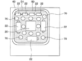
図6は、本発明の第5実施形態に係る電子装置S3の要部を示す図であり、(a)は、基板10の一面11側の概略平面図、(b)は、後述する応力緩和部材70およびその近傍部の部分概略断面図である。
(Fifth embodiment)
6A and 6B are diagrams showing the main part of an electronic device S3 according to a fifth embodiment of the present invention, where FIG. 6A is a schematic plan view of one
ダム部60内の補強用樹脂50のエリアすなわち第1の電子部品配置領域D1が大きくなると、応力が大きくなり、補強用樹脂50にクラックが発生する懸念がある。そこで、本実施形態では、ダム部60の内側にて補強用樹脂50の内部に、補強用樹脂50よりも弾性率の大きい応力緩和部材70を配置する。
When the area of the reinforcing
ここでは、応力緩和部材70は棒状をなすものであり、ダム部60と同様に、基板10の一面11に突出して設けられている。また、応力緩和部材70は、第1の電子部品配置領域D1内において、第1の電子部品20、22と重ならない位置、すなわち、第1の電子部品20、22とは異なる位置に設けられることが必要である。
Here, the
補強用樹脂50がエポキシ樹脂の場合には、応力緩和部材70の材料としては、シリコーン樹脂等が挙げられるが、同じエポキシ樹脂であっても、フィラーの量などを変えることで補強用樹脂50よりも弾性率が大きくなっているものであればよい。
In the case where the reinforcing
この応力緩和部材70は、基板10の一面11に、上記シリコーン樹脂等を塗布・硬化することにより形成される。その形成のタイミングとしては、たとえば、ダム部60の形成時に行ってもよいし、ダム部60を形成しさらに電子部品20〜22を実装した後に行ってもよい。要するに、補強用樹脂50の塗布前であればよい。
The
本実施形態によれば、第1の電子部品配置領域D1を広くしていくことで連続した1個の補強用樹脂50の配置面積が大きくなっても、応力緩和部材70によって、樹脂内部の応力を低減できるため、補強用樹脂50のクラックの発生防止が可能となる。
According to this embodiment, even if the arrangement area of one continuous reinforcing
図7は、本第5実施形態のもう一つの例としての電子装置の要部の概略平面構成を示す図であり、基板10の一面11側の概略平面図である。上記図6に示される例では、応力緩和部材70は棒状であったが、応力緩和部材70の形状は、図7に示されるように、球状であってもよい。この場合、棒状のものに比べて、必要な箇所に適宜配置しやすいという利点がある。また、これらの形状以外にも、応力緩和部材70の形状は、適宜変更が可能である。
FIG. 7 is a diagram showing a schematic plan configuration of a main part of an electronic device as another example of the fifth embodiment, and is a schematic plan view on the one
(他の実施形態)
なお、上記した各実施形態は、可能な範囲で適宜組み合わせてもよい。たとえば、基板10の一面11に、第1の電子部品配置領域D1を複数個設け、各領域D1について、補強用樹脂50の内部に応力緩和部材70を配置してもよい。
(Other embodiments)
In addition, you may combine each above-mentioned embodiment suitably in the possible range. For example, a plurality of first electronic component placement regions D1 may be provided on the one
10…基板、11…基板の一面、20…第1の電子部品としての第1の半導体素子、
21…第2の電子部品としての第2の半導体素子、
22…第1の電子部品としてのモールド素子、50…補強用樹脂、60…ダム部、
70…応力緩和部材、D1…第1の電子部品配置領域。
DESCRIPTION OF
21 ... Second semiconductor element as second electronic component,
22 ... Mold element as first electronic component, 50 ... Reinforcing resin, 60 ... Dam part,
70: Stress relaxation member, D1: First electronic component placement region.
Claims (4)
前記複数個の電子部品は、前記基板(10)との接続部が補強用樹脂(50)により補強されている第1の電子部品(20、22)と、前記基板(10)との接続部が前記補強用樹脂(50)により補強されていない第2の電子部品(21)とより構成されている電子装置において、
前記基板(10)の一面(11)には、複数個の前記第1の電子部品(20、22)が配置されるとともに前記第2の電子部品(21)は配置されない連続した1個の領域である第1の電子部品配置領域(D1)が設けられており、
この第1の電子部品配置領域(D1)の外周には、前記基板(10)の一面(11)における前記第1の電子部品配置領域(D1)の外側に前記補強用樹脂(50)がはみ出すのを防止するダム部(60)が設けられており、
前記ダム部(60)の内側にて前記補強用樹脂(50)の内部には、前記補強用樹脂(50)よりも弾性率の大きい応力緩和部材(70)が配置されていることを特徴とする電子装置。 A plurality of electronic components (20, 21, 22) are mounted on one surface (11) of the substrate (10), and the substrate (10) and the plurality of electronic components (20-22) are connected,
The plurality of electronic components are connected to the substrate (10) and the first electronic component (20, 22) in which the connection to the substrate (10) is reinforced by a reinforcing resin (50). In the electronic device constituted by the second electronic component (21) which is not reinforced by the reinforcing resin (50),
On one surface (11) of the substrate (10), a plurality of the first electronic components (20, 22) are arranged and one continuous region where the second electronic components (21) are not arranged. A first electronic component placement region (D1) is provided,
On the outer periphery of the first electronic component placement region (D1), the reinforcing resin (50) protrudes outside the first electronic component placement region (D1) on one surface (11) of the substrate (10). A dam (60) is provided to prevent
A stress relaxation member (70) having a higher elastic modulus than the reinforcing resin (50) is disposed inside the reinforcing resin (50) inside the dam portion (60). Electronic device to play.
Priority Applications (1)
| Application Number | Priority Date | Filing Date | Title |
|---|---|---|---|
| JP2012154887A JP5673616B2 (en) | 2012-07-10 | 2012-07-10 | Electronic equipment |
Applications Claiming Priority (1)
| Application Number | Priority Date | Filing Date | Title |
|---|---|---|---|
| JP2012154887A JP5673616B2 (en) | 2012-07-10 | 2012-07-10 | Electronic equipment |
Related Parent Applications (1)
| Application Number | Title | Priority Date | Filing Date |
|---|---|---|---|
| JP2007273787A Division JP5115144B2 (en) | 2007-10-22 | 2007-10-22 | Electronic equipment |
Publications (2)
| Publication Number | Publication Date |
|---|---|
| JP2012195615A true JP2012195615A (en) | 2012-10-11 |
| JP5673616B2 JP5673616B2 (en) | 2015-02-18 |
Family
ID=47087162
Family Applications (1)
| Application Number | Title | Priority Date | Filing Date |
|---|---|---|---|
| JP2012154887A Expired - Fee Related JP5673616B2 (en) | 2012-07-10 | 2012-07-10 | Electronic equipment |
Country Status (1)
| Country | Link |
|---|---|
| JP (1) | JP5673616B2 (en) |
Cited By (2)
| Publication number | Priority date | Publication date | Assignee | Title |
|---|---|---|---|---|
| JP2014179391A (en) * | 2013-03-14 | 2014-09-25 | Honda Motor Co Ltd | Protection structure for electronic substrate |
| JP2017041603A (en) * | 2015-08-21 | 2017-02-23 | ルネサスエレクトロニクス株式会社 | Semiconductor device |
Citations (11)
| Publication number | Priority date | Publication date | Assignee | Title |
|---|---|---|---|---|
| JPS5982750A (en) * | 1982-11-02 | 1984-05-12 | Nec Corp | High density ceramic package |
| JPS59131160U (en) * | 1983-02-21 | 1984-09-03 | 三菱電機株式会社 | Hybrid integrated circuit device |
| JPS62147752A (en) * | 1985-12-20 | 1987-07-01 | Nec Corp | Semiconductor device |
| JPS6362297A (en) * | 1986-09-02 | 1988-03-18 | 信越ポリマ−株式会社 | Method of mounting electronic parts |
| JPH05160296A (en) * | 1991-12-04 | 1993-06-25 | Ibiden Co Ltd | Resin sealing method of semiconductor integrated circuit bare chip |
| JPH07335825A (en) * | 1994-06-10 | 1995-12-22 | Mitsubishi Electric Corp | Hybrid integrated circuit and its fabricating method |
| JPH09293743A (en) * | 1996-04-26 | 1997-11-11 | Mitsubishi Electric Corp | Manufacture of bare chip mold part and bare chip mold part manufactured by it |
| JPH1093011A (en) * | 1996-09-19 | 1998-04-10 | Matsushita Electric Ind Co Ltd | Lightening surge protective device |
| JP2000228482A (en) * | 1999-02-05 | 2000-08-15 | Denso Corp | Hybrid integrated circuit device |
| JP2003142523A (en) * | 2001-10-31 | 2003-05-16 | Toshiba Corp | Electronic component and method for manufacturing the same |
| JP2004200278A (en) * | 2002-12-17 | 2004-07-15 | Sanyo Electric Co Ltd | Circuit board assembly |
-
2012
- 2012-07-10 JP JP2012154887A patent/JP5673616B2/en not_active Expired - Fee Related
Patent Citations (11)
| Publication number | Priority date | Publication date | Assignee | Title |
|---|---|---|---|---|
| JPS5982750A (en) * | 1982-11-02 | 1984-05-12 | Nec Corp | High density ceramic package |
| JPS59131160U (en) * | 1983-02-21 | 1984-09-03 | 三菱電機株式会社 | Hybrid integrated circuit device |
| JPS62147752A (en) * | 1985-12-20 | 1987-07-01 | Nec Corp | Semiconductor device |
| JPS6362297A (en) * | 1986-09-02 | 1988-03-18 | 信越ポリマ−株式会社 | Method of mounting electronic parts |
| JPH05160296A (en) * | 1991-12-04 | 1993-06-25 | Ibiden Co Ltd | Resin sealing method of semiconductor integrated circuit bare chip |
| JPH07335825A (en) * | 1994-06-10 | 1995-12-22 | Mitsubishi Electric Corp | Hybrid integrated circuit and its fabricating method |
| JPH09293743A (en) * | 1996-04-26 | 1997-11-11 | Mitsubishi Electric Corp | Manufacture of bare chip mold part and bare chip mold part manufactured by it |
| JPH1093011A (en) * | 1996-09-19 | 1998-04-10 | Matsushita Electric Ind Co Ltd | Lightening surge protective device |
| JP2000228482A (en) * | 1999-02-05 | 2000-08-15 | Denso Corp | Hybrid integrated circuit device |
| JP2003142523A (en) * | 2001-10-31 | 2003-05-16 | Toshiba Corp | Electronic component and method for manufacturing the same |
| JP2004200278A (en) * | 2002-12-17 | 2004-07-15 | Sanyo Electric Co Ltd | Circuit board assembly |
Cited By (3)
| Publication number | Priority date | Publication date | Assignee | Title |
|---|---|---|---|---|
| JP2014179391A (en) * | 2013-03-14 | 2014-09-25 | Honda Motor Co Ltd | Protection structure for electronic substrate |
| JP2017041603A (en) * | 2015-08-21 | 2017-02-23 | ルネサスエレクトロニクス株式会社 | Semiconductor device |
| US10553558B2 (en) | 2015-08-21 | 2020-02-04 | Renesas Electronics Corporation | Semiconductor device |
Also Published As
| Publication number | Publication date |
|---|---|
| JP5673616B2 (en) | 2015-02-18 |
Similar Documents
| Publication | Publication Date | Title |
|---|---|---|
| CN104779217A (en) | Semiconductor device package with warpage control structure | |
| JP2012129464A (en) | Semiconductor device and method of manufacturing the same | |
| JP2007281129A (en) | Stacked semiconductor device | |
| JP2013236039A (en) | Semiconductor device | |
| CN110459521B (en) | Flip chip package substrate and electronic package | |
| JP2009049218A (en) | Semiconductor device, and manufacturing method of semiconductor device | |
| WO2018126545A1 (en) | Electronic package structure with high reliability, circuit board and device | |
| US20120319255A1 (en) | Thermal Enhanced High Density Flip Chip Package | |
| JP5973461B2 (en) | Expandable semiconductor chip and semiconductor device | |
| US9793237B2 (en) | Hollow-cavity flip-chip package with reinforced interconnects and process for making the same | |
| JP5115144B2 (en) | Electronic equipment | |
| JP5673616B2 (en) | Electronic equipment | |
| US20130048351A1 (en) | Electronic package structure and method for manufacturing same | |
| JP5115269B2 (en) | Semiconductor device mounting structure and electronic device using the mounting structure | |
| KR20120053386A (en) | Lead pin for package substrate and package substrate using the same | |
| US20140167276A1 (en) | Substrate for semiconductor package, semiconductor package using the substrate, and method of manufacturing the semiconductor package | |
| JP6391430B2 (en) | Electronic control device and manufacturing method thereof | |
| JP2008251929A (en) | Multilayer type semiconductor device | |
| JP2008047699A (en) | Semiconductor device and its manufacturing method | |
| KR20120062434A (en) | Semiconductor package and method for manufacturing the same | |
| JP2011249398A (en) | Circuit device | |
| JP2011003818A (en) | Mold package | |
| JP2010267792A (en) | Semiconductor device and manufacturing method therefor | |
| JP2009070898A (en) | Component mounting substrate, electronic device, and component mounting method | |
| JP2015153985A (en) | semiconductor package |
Legal Events
| Date | Code | Title | Description |
|---|---|---|---|
| A621 | Written request for application examination |
Free format text: JAPANESE INTERMEDIATE CODE: A621 Effective date: 20120711 |
|
| A977 | Report on retrieval |
Free format text: JAPANESE INTERMEDIATE CODE: A971007 Effective date: 20130307 |
|
| A131 | Notification of reasons for refusal |
Free format text: JAPANESE INTERMEDIATE CODE: A131 Effective date: 20130409 |
|
| A521 | Written amendment |
Free format text: JAPANESE INTERMEDIATE CODE: A523 Effective date: 20130528 |
|
| A131 | Notification of reasons for refusal |
Free format text: JAPANESE INTERMEDIATE CODE: A131 Effective date: 20140225 |
|
| A521 | Written amendment |
Free format text: JAPANESE INTERMEDIATE CODE: A523 Effective date: 20140414 |
|
| TRDD | Decision of grant or rejection written | ||
| A01 | Written decision to grant a patent or to grant a registration (utility model) |
Free format text: JAPANESE INTERMEDIATE CODE: A01 Effective date: 20141202 |
|
| A61 | First payment of annual fees (during grant procedure) |
Free format text: JAPANESE INTERMEDIATE CODE: A61 Effective date: 20141215 |
|
| R151 | Written notification of patent or utility model registration |
Ref document number: 5673616 Country of ref document: JP Free format text: JAPANESE INTERMEDIATE CODE: R151 |
|
| R250 | Receipt of annual fees |
Free format text: JAPANESE INTERMEDIATE CODE: R250 |
|
| R250 | Receipt of annual fees |
Free format text: JAPANESE INTERMEDIATE CODE: R250 |
|
| R250 | Receipt of annual fees |
Free format text: JAPANESE INTERMEDIATE CODE: R250 |
|
| LAPS | Cancellation because of no payment of annual fees |