JP2012190841A - Led package and led lighting device - Google Patents
Led package and led lighting device Download PDFInfo
- Publication number
- JP2012190841A JP2012190841A JP2011050570A JP2011050570A JP2012190841A JP 2012190841 A JP2012190841 A JP 2012190841A JP 2011050570 A JP2011050570 A JP 2011050570A JP 2011050570 A JP2011050570 A JP 2011050570A JP 2012190841 A JP2012190841 A JP 2012190841A
- Authority
- JP
- Japan
- Prior art keywords
- support
- led
- circuit board
- led chip
- wiring pattern
- Prior art date
- Legal status (The legal status is an assumption and is not a legal conclusion. Google has not performed a legal analysis and makes no representation as to the accuracy of the status listed.)
- Pending
Links
Images
Landscapes
- Arrangement Of Elements, Cooling, Sealing, Or The Like Of Lighting Devices (AREA)
- Led Device Packages (AREA)
Abstract
【課題】LEDチップの発熱を効率よく放熱することができ、信頼性の向上及び大型化を実現することができるLEDパッケージ及びLED照明装置を実現すること。
【解決手段】LEDパッケージ100は、LEDチップ110と、LEDチップ110を載置面120aに支持するセラミックからなる支持体120と、支持体120の裏面120bに形成され、回路基板170上の配線パターン160と電気的に絶縁された放熱用金属膜130と、支持体120に設置されたLEDチップ110と回路基板170とを電気的に接続する導体配線140,150と、を備える。放熱用金属膜130は、支持体120の裏面120bと回路基板170とを熱的に接続する。
【選択図】図2An LED package and an LED lighting device capable of efficiently dissipating heat generated from an LED chip and improving reliability and increasing size.
An LED package (100) is formed on an LED chip (110), a support body (120) made of ceramic that supports the LED chip (110) on a mounting surface (120a), and a back surface (120b) of the support body (120). The heat-dissipating metal film 130 is electrically insulated from 160, and the conductor wirings 140 and 150 that electrically connect the LED chip 110 and the circuit board 170 installed on the support 120. The heat dissipation metal film 130 thermally connects the back surface 120b of the support 120 and the circuit board 170.
[Selection] Figure 2
Description
本発明は、LED(Light Emitting Diode)チップを支持体に搭載するパッケージ及びLED照明装置に関する。 The present invention relates to a package for mounting an LED (Light Emitting Diode) chip on a support and an LED lighting device.
近年、数十μmから数mm程度角の大きさのLEDチップをパッケージ内に収めた発光装置が開発され、電子機器、車両、各種の照明装置として利用が拡大している。 In recent years, a light emitting device in which an LED chip having a size of about several tens of μm to several mm is housed in a package, and its use is expanding as an electronic device, a vehicle, and various lighting devices.
LEDチップは、導体配線が施された支持体に搭載される。LEDの高出力化に伴い、支持体は、耐熱性及び耐光性に優れたセラミックスを主な材料とするセラミックパッケージが好適に利用されている。 The LED chip is mounted on a support body provided with conductor wiring. Along with the increase in the output of the LED, a ceramic package mainly made of ceramics having excellent heat resistance and light resistance is preferably used as the support.
上記支持体に施された導体配線は、LEDチップと外部の電極とを電気的に接続するだけではなく、発光装置の放熱性を向上させることができる。 The conductor wiring provided on the support not only electrically connects the LED chip and external electrodes, but can also improve the heat dissipation of the light emitting device.
特許文献1には、半導体素子と、その半導体素子を配置し、該半導体素子の電極に接続される導体配線が設けられたパッケージと、を備える半導体装置が記載されている。特許文献1記載の半導体装置は、セラミックスのような光の吸収が顕著な材料を用いたLEDパッケージに搭載された半導体装置においても、光の漏れ及び吸収を最小限にとどめ、簡便な構成により、光取り出し効率を向上させようとする。 Patent Document 1 describes a semiconductor device that includes a semiconductor element and a package in which the semiconductor element is arranged and a conductor wiring connected to an electrode of the semiconductor element is provided. The semiconductor device described in Patent Document 1 is a semiconductor device mounted on an LED package using a material such as ceramics that has a significant light absorption. Try to improve the light extraction efficiency.
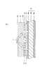
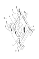
図1は、特許文献1記載の半導体装置を搭載したLEDパッケージを模式的に示す断面図である。図1中の矢印は、LEDチップの発熱を放熱する主要な放熱ルートを示している。 FIG. 1 is a cross-sectional view schematically showing an LED package on which a semiconductor device described in Patent Document 1 is mounted. The arrows in FIG. 1 indicate main heat dissipation routes for dissipating the heat generated by the LED chip.
図1に示すように、LEDパッケージ10は、LEDチップ11と、LEDチップ11を載置面12aに支持するセラミックからなる支持体12と、支持体12の裏面12bに接着剤により貼り付けられた導体配線13,14と、銅箔からなる配線パターン15が形成された回路基板16と、を備える。
As shown in FIG. 1, the LED package 10 is affixed to the
LEDチップ11は、支持体12内部に施された配線(図示略)により導体配線13,14に接続されている。
The
支持体12は、LEDチップ11を支持する土台としての機能を有する。支持体12は、セラミックが好適に利用される。支持体12をセラミックにより形成する場合、支持体12は、通常、貫通孔を設けたりして種々のパターン形状に形成した複数の未焼成セラミックグリーンシートを積層させた後、焼成することにより作製される。
The
支持体12は、土台としての機能を有する。また、支持体12は、LEDチップ11の載置面を開口させるように形成することによって、リフレクタとしても機能させることができる。
The
導体配線13,14は、LEDチップ11の正負の各電極と配線パターン15とを接続する一対の配線電極である。また、導体配線13,14は、LEDチップ11から支持体12に伝導した熱を、回路基板16側に放熱する機能を併せ持つ。
The
回路基板16は、例えば、伝熱率が低い第1絶縁層16aと、伝熱率が高い金属層16bと、伝熱率が低い第2絶縁層16cとが積層されている。
The
以上のように構成された特許文献1記載の半導体装置は、LEDチップ11の放熱に際して、以下の課題がある。
The semiconductor device described in Patent Document 1 configured as described above has the following problems when the
LEDは回路基板に搭載されるが、このLEDは、他の半導体素子と比較して発熱が非常に大きい。 The LED is mounted on a circuit board, but this LED generates much heat as compared with other semiconductor elements.
特許文献1記載の半導体装置は、LEDチップ11の発熱を放熱するために、LEDチップ11の熱を、支持体12の裏面に形成された導体配線13,14を介して配線パターン15、さらには回路基板16へ伝達する。
In the semiconductor device described in Patent Document 1, in order to dissipate heat generated by the
しかしながら、導体配線13,14は、LEDチップ11の電極端子であるため、絶対にショートしてはならないという制約がある。そこで、導体配線13,14は、正負一対の各電極であることから、両者の間には、図1に示すように、支持体12の裏面と導体配線13,14と回路基板16上で囲まれた空気の層(ギャップ)17が形成されることになる。
However, since the
上記構成上の制約のため、放熱効果を向上させるために導体配線13,14の配線面積を大きくしようとしても、必ず導体配線13,14同士の間にギャップ17を形成しなければならないことから、一定の配線面積以上に導体配線13,14を大きく形成することはできない。したがって、導体配線13,14を用いた放熱効果を向上させることには限界がある。
Because of the limitations on the configuration described above, the
しかも、図1に示すように、LEDチップ11は、一般的に支持体12の載置面12aの中心に配置されるのに対して、導体配線13,14は、LEDチップ11の配置位置(支持体12の載置面12aの中心位置)から離れた位置に形成されている。このため、図1矢印の放熱ルートに示すように、LEDチップ11の発熱は、導体配線13,14を伝導して迂回する形で回路基板16側に伝達される。つまり、LEDチップ11の発熱を最短路で回路基板16へ送達できないので、放熱効果が悪いという課題がある。
In addition, as shown in FIG. 1, the
さらに、導体配線13,14の配線面積を大きくすることができない別の要因がある。すなわち、導体配線13,14の配線面積を大きく形成すると、導体配線13,14と配線パターン15との接続、並びに導体配線13,14とセラミックからなる支持体12との接続が、熱膨張による応力に耐えられなくなるという課題がある。例えば、回路基板16(組成:金属/熱膨張率大)と、支持体12(組成:セラミック/熱膨張率小)との熱膨張率の差により、固定部分である導体配線13,14部分に大きな応力がかかる。特に大口径のLEDパッケージになると、回路基板16と支持体12との膨張の差が大きくなりすぎて、接合材の半田などの固定部材が応力に耐えられずクラックが生じたり、破損する虞がある。同様の不具合は、支持体12と回路基板16とを接着する樹脂等の接着剤にも生じる。以上のことから、大口径のLEDパッケージを作製するのが困難であるという課題がある。
Furthermore, there is another factor that the wiring area of the
本発明の目的は、LEDチップの発熱を効率よく放熱することができ、信頼性の向上及び大型化を実現することができるLEDパッケージ及びLED照明装置を提供することである。 An object of the present invention is to provide an LED package and an LED lighting device that can efficiently dissipate heat generated from an LED chip, and that can improve reliability and increase in size.
本発明のLEDパッケージは、配線パターンを形成した回路基板に載置されるLEDパッケージであって、LEDチップを搭載し前記LEDチップに接続する制御用配線を表面に形成した支持体と、前記支持体端部に設けられ、前記制御用配線を電気的に前記配線パターンに接続する導体配線部と、前記支持体の裏面に設けられ、前記支持体を熱的に前記回路基板に接続する放熱用金属膜とを有する、構成を採る。 The LED package of the present invention is an LED package mounted on a circuit board on which a wiring pattern is formed, the support having the LED chip mounted thereon and the control wiring connected to the LED chip formed on the surface, and the support Conductive wiring provided at the end of the body for electrically connecting the control wiring to the wiring pattern, and for heat dissipation provided on the back surface of the support for thermally connecting the support to the circuit board The structure which has a metal film is taken.
本発明のLED照明装置は、配線パターンを形成した回路基板と、LEDチップを搭載し前記LEDチップに接続する制御用配線を表面に形成した支持体と、前記支持体端部に設けられ前記制御用配線を電気的に前記配線パターンに接続する導体配線部と、前記支持体の裏面に設けられ前記支持体を熱的に前記回路基板に接続する放熱用金属膜と、を有するLEDパッケージとを有し、前記LEDチップの制御用配線と前記回路基板の配線パターンとを接続するとともに、前記支持体を前記放熱用金属膜を介して前記回路基板に接続し、前記配線パターンと前記放熱用金属膜とは相互に絶縁されている、構成を採る。 The LED lighting device of the present invention includes a circuit board on which a wiring pattern is formed, a support on which an LED chip is mounted and a control wiring connected to the LED chip is formed on the surface, and the control provided on the end of the support An LED package comprising: a conductor wiring portion that electrically connects the wiring for wiring to the wiring pattern; and a heat dissipating metal film that is provided on the back surface of the support and thermally connects the support to the circuit board. And connecting the control wiring of the LED chip and the wiring pattern of the circuit board, and connecting the support to the circuit board via the metal film for heat dissipation, the wiring pattern and the metal for heat dissipation. The film is insulated from each other.
本発明によれば、LEDチップの発熱を効率よく放熱することができ、信頼性の向上及び大型化を実現することができるLEDパッケージを実現することができる。 ADVANTAGE OF THE INVENTION According to this invention, the LED package which can thermally radiate the heat | fever of an LED chip efficiently and can implement | achieve an improvement in reliability and enlargement is realizable.
以下、本発明の実施の形態について、図面を参照して詳細に説明する。 Hereinafter, embodiments of the present invention will be described in detail with reference to the drawings.
(実施の形態1)
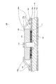
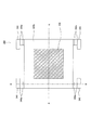
図2は、本発明の実施の形態1に係るLEDパッケージを模式的に示す断面図である。図1中の矢印は、LEDチップの発熱を放熱する主要な放熱ルートを示している。以下、本発明に係るLEDパッケージを、セラミックLEDパッケージで具現化した例で説明する。
(Embodiment 1)
FIG. 2 is a cross-sectional view schematically showing the LED package according to Embodiment 1 of the present invention. The arrows in FIG. 1 indicate main heat dissipation routes for dissipating the heat generated by the LED chip. Hereinafter, an LED package according to the present invention will be described with an example of a ceramic LED package.
図2に示すように、LEDパッケージ100は、銅箔からなる配線パターン160が形成された回路基板170上に設置される。
As shown in FIG. 2, the
LEDパッケージ100は、LEDチップ110と、LEDチップ110を載置面120aに支持するセラミックからなる支持体120と、支持体120の裏面120bに形成され、回路基板170上の配線パターンと電気的に絶縁される放熱用金属膜130と、支持体120に設置されたLEDチップ110と回路基板170上に形成された配線パターン160とを電気的に接続する導体配線140,150と、を備える。
The
LEDチップ110は、支持体120に施された配線(図示略)により導体配線140,150に接続されている。
The
支持体120は、LEDチップ110を支持する土台としての機能を有する。支持体120は、セラミックが好適に利用される。また、セラミックには、安価で絶縁性、反射率、熱伝導率に優れ、熱やUV(Ultra Violet)による劣化の少ないアルミナが好適である。他のセラミックには、各種酸化物、窒化物、酸窒化物、炭化物などが用いられる。セラミック支持体は、通常、貫通孔を設けたりして種々のパターン形状に形成した複数の未焼成セラミックグリーンシートを積層させた後、焼成することにより作製される。なお、セラミックの他、適用可能な材料には、BTレジン(ビスマレイミドトリアジン樹脂)、ガラスエポキシ樹脂、フェノール樹脂等が挙げられる。
The
また、支持体120は、LEDチップ110の載置面を開口させるように形成することによって、リフレクタとしても機能させることができる。この例については、実施の形態3により後述する。
Moreover, the
放熱用金属膜130は、LEDチップ110の発熱を放熱する放熱用の金属パッドである。
The heat
放熱用金属膜130は、支持体120の裏面120bと配線パターン160又は金属層170bとを直付けする。
The heat
放熱用金属膜130は、放熱の目的のためだけに設置されており、電気的には絶縁されている。すなわち、放熱用金属膜130は、支持体120の裏面120bと回路基板170の金属層170bとを直付けして熱を伝達する一方、配線パターン160等の導体からは分離されて電気的絶縁が保たれる。放熱用金属膜130は、いわば熱的に、支持体120と回路基板170とを接続している。
The heat dissipating
放熱用金属膜130は、例えば下地Cu/Ni/Auが好適である。また、放熱用金属膜130は、AgやNi/Pd/Au、Ni/Auなどが使用可能である。
The heat
放熱用金属膜130は、放熱効果を高める観点から、より広い面積で回路基板170の金属層170b上に接合されることが好ましい。本実施の形態では、放熱用金属膜130は、支持体120の裏面120bのほぼ全面に、例えばCu電解メッキにより形成されている。
It is preferable that the
導体配線140,150は、LEDチップ110の正負の各電極と配線パターン160とを接続する一対の配線電極(LF:リードフレーム)である。導体配線140,150は、熱膨張率の差による応力を吸収する曲げ部分140a,150aを有する。導体配線140,150は、支持体120のコーナー部に形成されていること、高温の支持体120との接触面積が小さいこと、曲げ部分140a,150aから空間への放熱が可能であること等のため、LEDの直下に導体配線を配置する従来のLEDパッケージと比較すると、LEDチップ110の熱は構造的に配線パターン160との接合部に伝達し難い。そのため、導体配線140,150は、銅箔で形成された配線パターン160とは熱膨張率が異なるが、その接合部に過度の応力が発生することがないため、接続部が切断、破損することはない。更に、接合部に多少の応力が生ずる場合でも、導体配線140,150のリード部の曲げ部分140a,150aがこれを吸収する。
The conductor wirings 140 and 150 are a pair of wiring electrodes (LF: lead frame) that connect the positive and negative electrodes of the
導体配線140,150は、例えば無酸素銅又は、脱酸素銅を主材料とした銅合金に、光の反射率を上げるため、Agなどの反射率の高い材料でめっきを施すものが好適である。また、導体配線140,150は、無酸素銅、脱酸素銅、銅合金、又はFe系の材料などの金属材料を用いてもよい。 For the conductor wirings 140 and 150, for example, oxygen-free copper or a copper alloy mainly containing deoxygenated copper is preferably plated with a highly reflective material such as Ag in order to increase the light reflectance. . The conductor wirings 140 and 150 may be made of a metal material such as oxygen-free copper, oxygen-free copper, a copper alloy, or an Fe-based material.
また、導体配線140,150は、LEDチップ110の配線電極としての機能を有することを主目的とするが、LEDチップ110の発熱を、回路基板170側に放熱する副次的な機能も持つ。
The conductor wirings 140 and 150 mainly have a function as a wiring electrode of the
配線パターン160は、回路基板170の第1絶縁層170a上に部分めっき処理などにより形成されている。配線パターン160には、導体配線140,150の端部が半田などにより接続されている。本実施の形態では、配線パターン160は、
The
回路基板170は、伝熱率が低い第1絶縁層170aと、伝熱率が高い金属層170bと、伝熱率が低い第2絶縁層170cとが積層されている。第1絶縁層170aには、放熱用金属膜130を、金属層170bに直付けするための開口部171が形成されている。
The
以下、上述のように構成されたLEDパッケージの作製方法について説明する。 Hereinafter, a manufacturing method of the LED package configured as described above will be described.
放熱用金属膜130は、配線電極である導体配線140,150とは別体で、支持体120に裏面120b形成するものである。
The heat radiating
それぞれの部品の形成方法は、以下の通りである。 The method of forming each component is as follows.
支持体120は、乾式成形機により材料を成形し、焼結することで得られる。又は、ドクターブレードを用いた湿式成形により、シートを成形し、焼結後、カッティングすることにより形成する。支持体120上の配線である上面金属(図示略)は、例えば、Cu/Ni/Auを部分めっき処理することにより得られる。
The
放熱用金属膜130は、例えばCu電解めっき処理により形成する。
The heat
導体配線140,150は、圧延加工した金属リードフレームをスタンピング(打ち抜き)加工や曲げ加工等を金型を用いて段階的に実施する。 For the conductor wirings 140 and 150, stamped (bending) processing and bending processing of the rolled metal lead frame is performed step by step using a mold.
また、放熱用金属膜130は、支持体120と、配線パターン160又は回路基板170の金属層170bとを完全に接着させる。この場合、あらかじめ支持体120に放熱用金属膜130をめっき処理又は蒸着処理などによって形成しておくようにする。このような前処理をしておくと、放熱用金属膜130と配線パターン160又は回路基板170の金属層170bとを、半田によって完全に接続することができる。
The heat
以上詳細に説明したように、本実施の形態のLEDパッケージ100は、LEDチップ110と、LEDチップ110を載置面120aに支持するセラミックからなる支持体120と、支持体120の裏面120bに形成され、回路基板170上の配線パターン160と電気的に絶縁された放熱用金属膜130と、支持体120に設置されたLEDチップ110と回路基板170とを電気的に接続する導体配線140,150と、を備える。放熱用金属膜130は、支持体120の裏面120bと回路基板170の金属層170bとを直付けする。
As described in detail above, the
このように、LEDパッケージ100は、配線電極である導体配線140,150とは別体で、放熱用金属膜130として支持体120に新たに形成する。放熱用金属膜130は、支持体120の裏面120bと回路基板170の金属層170bとを直付けしている。
In this way, the
図2の矢印に示すように、LEDパッケージ100は、支持体120の裏面120bと回路基板170の金属層170bとを直付けした放熱用金属膜130が、LEDチップ110の発熱を回路基板170側に速やかに放熱する。放熱用金属膜130は、LEDチップ110の放熱のみを目的とするため、回路基板170上の配線パターン160とは電気的な絶縁が保たれている。このため短絡等の電気的な影響はない。
As shown by the arrows in FIG. 2, the
特に、放熱用金属膜130は、電気的に絶縁されているため、回路基板170の金属層170b部分に直接接続して放熱することができる。
In particular, since the heat dissipating
その結果、LEDチップ110の発熱を効率よく放熱することができ、熱膨張による応力による破損を未然に防止して信頼性の向上を図ることができると共に、大型化を実現することができる。
As a result, heat generated by the
ここで、放熱用金属膜130は、回路基板170の金属層170b部分ではなく、配線パターン160とは電気的に絶縁された第2配線パターンと接続して放熱する態様でもよい。なお、この例は実施の形態2により説明する。放熱用金属膜130を配線パターン160接続して放熱するようにすれば、回路基板170の表面上に直接放熱することができる。
Here, the heat radiating
また、本実施の形のLEDパッケージ100は、LEDチップ110が、支持体120のどこに配置されても、放熱用金属膜130を介して、その裏面120bから回路基板170側にダイレクトに放熱することができる利点がある。
Further, in the
また、本実施の形のLEDパッケージ100は、導体配線140,150の上記構造により、LEDチップ110の熱は構造的に配線パターン160との接合部に伝達し難い。そのため、配線パターン160との接合部に過度の応力が発生することがないため、接続部が切断、破損することはない。更に、接合部に多少の応力が生ずる場合でも、導体配線140,150のリード部の曲げ部分140a,150aがこれを吸収する。これらにより、LEDパッケージの大型化を実現できる。
Further, in the
なお、本実施の形態では、回路基板170の第1絶縁層170a上に、配線パターン160を形成しているが、配線パターン160を有する回路基板であれば、どのような基板でもよい。
In the present embodiment, the
(実施の形態2)
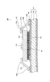
図3は、本発明の実施の形態2に係るLEDパッケージを模式的に示す断面図である。図2と同一構成部分には同一符号を付して重複箇所の説明を省略する。実施の形態1との相違は、導電配線に接続する配線パターン以外に、他の配線パターンが回路基板上に形成されている点にある。この場合でも、実施の形態1同様に本発明を適用できる。
(Embodiment 2)
FIG. 3 is a cross-sectional view schematically showing an LED package according to Embodiment 2 of the present invention. The same components as those in FIG. 2 are denoted by the same reference numerals, and description of overlapping portions is omitted. The difference from the first embodiment is that, in addition to the wiring pattern connected to the conductive wiring, another wiring pattern is formed on the circuit board. Even in this case, the present invention can be applied as in the first embodiment.
図3に示すように、LEDパッケージ100は、銅箔からなる配線パターン160と、配線パターン160とは電気的に絶縁された第2配線パターン161とが形成された回路基板171上に設置される。
As shown in FIG. 3, the
回路基板171は、伝熱率が低い第1絶縁層171aと、伝熱率が高い金属層171bと、伝熱率が低い第2絶縁層171cとが積層されている。
The
配線パターン161及び第2配線パターン161は、回路基板171の第1絶縁層171a上に部分めっき処理などにより形成されている。配線パターン160には、導体配線140,150の端部が半田などにより接続されている。
The
第2配線パターン161は、配線パターン160とは電気的に絶縁され、少なくとも一部が回路基板171上の放熱用金属膜130直下まで延びている。この第2配線パターン161は、例えばGNDに接続されている。
The
放熱用金属膜130は、支持体120の裏面120bと回路基板171上の第2配線パターン161とを直付けする。
The heat
したがって、本実施の形態では、実施の形態1と同様の効果、すなわちLEDチップ110の発熱を効率よく放熱することができ、信頼性の向上及び大型化を実現することができるLEDパッケージを得ることができる。
Therefore, in the present embodiment, the same effect as in the first embodiment, that is, an LED package that can efficiently dissipate the heat generated by the
特に、本実施の形態では、第2絶縁層171c上の第1絶縁層171aを、放熱用金属膜130の形状に合わせて、取り除く工程(マスキング工程、エッチング工程など)が不要になるため、コスト低減が期待できる。また、従来の回路基板上の配線パターンの変更で済むので、この点からもコスト低減を図ることができ、また実施が容易である利点がある。
In particular, in this embodiment, a process (masking process, etching process, etc.) for removing the first insulating
なお、放熱用金属膜130は、電気的な意味をもたないため、LEDチップ110に接続する導体配線140,150のうちの一方、例えば一方の導体配線140が、放熱用金属膜130の直下に形成された第2配線パターン161に接続されていてもよい。
Since the heat
(実施の形態3)
図4は、本発明の実施の形態3に係るLEDパッケージを模式的に示す断面図である。図2と同一構成部分には同一符号を付して重複箇所の説明を省略する。
(Embodiment 3)
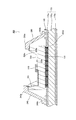
FIG. 4 is a cross-sectional view schematically showing an LED package according to Embodiment 3 of the present invention. The same components as those in FIG. 2 are denoted by the same reference numerals, and description of overlapping portions is omitted.
図4に示すように、LEDパッケージ200は、配線パターン160が形成された回路基板170上に設置される。
As shown in FIG. 4, the
LEDパッケージ200は、LEDチップ110と、LEDチップ110を載置面220aに支持するセラミックからなる支持体220と、支持体220の裏面220dに形成され、回路基板170と電気的に絶縁された放熱用金属膜130と、支持体220に設置されたLEDチップ110と回路基板170とを電気的に接続する導体配線240,250と、を備える。
The
LEDチップ110は、支持体220内部のスルーホール配線221により導体配線240,250に接続されている。
The
支持体220は、LEDチップ110を支持する土台としての機能を有する。支持体220は、セラミックが好適に利用される。
The
支持体220は、LEDチップ110が載置された第1面である載置面220aと、LEDチップ110の周囲にあって載置面220a(第1面)よりも外部に突出した第2面220bとを有する段差構造を備える。載置面220aと第2面220bとの間の側面220cは、LEDチップ110が発光した光を反射するリフレクタを形成している。すなわち、支持体220は、LEDチップ110の載置面220aを開口させるように形成することによって、リフレクタとしても機能させている。
The
したがって、本実施の形態では、実施の形態1の効果に加え、支持体220をリフレクタとしても機能させているので、LEDチップ110の横方向へ発光を前方方向に反射させることができ、利用できる発光を増大させることができる。これによりLEDパッケージ200による発光品位を向上させることができる。
Therefore, in this embodiment, in addition to the effects of the first embodiment, the
(実施の形態4)
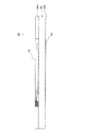
図5は、本発明の実施の形態4に係るLEDパッケージの構造を示す斜視図である。図6は、図5のLEDパッケージの支持体を背面からみた平面図、図7は、図6のA−A矢視断面図、図8は、図6のB−B矢視断面図である。
(Embodiment 4)
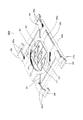
FIG. 5 is a perspective view showing the structure of an LED package according to Embodiment 4 of the present invention. 6 is a plan view of the support body of the LED package of FIG. 5 as viewed from the back, FIG. 7 is a cross-sectional view taken along the line AA in FIG. 6, and FIG. 8 is a cross-sectional view taken along the line BB in FIG. .
図5乃至図8に示すように、LEDパッケージ300は、LEDチップ310と、LEDチップ310を載置面320aに支持するセラミックからなる支持体320と、支持体320の裏面320bに形成され、図示しない回路基板上の配線パターンと電気的に絶縁された放熱用金属膜330(図6乃至図8参照)と、支持体320に設置されたLEDチップ310と回路基板(図示略)とを電気的に接続する導体配線340,350と、LEDチップ310の周囲を囲むように配置され、LEDチップ310が発光した光を反射するリフレクタ360と、を備える。
As shown in FIGS. 5 to 8, the
LEDチップ310は、支持体320に施された配線321により導体配線340,350に接続されている。
The
支持体320は、LEDチップ310を支持するセラミック基板である。
The
放熱用金属膜330は、LEDチップ310の発熱を放熱する放熱用の金属パッドである。
The heat
放熱用金属膜330は、支持体320の裏面320bと図示しない回路基板の配線パターン又は金属層とを直付けする。放熱用金属膜330は、放熱の目的のためだけに設置されており、回路基板上の配線パターンとは電気的には絶縁されている。
The heat
放熱用金属膜330は、例えば下地Cu/Ni/Auが好適である。また、放熱用金属膜330は、AgやNi/Pd/Au、Ni/Auなどが使用可能である。
The heat
図6乃至図8に示すように、放熱用金属膜130は、放熱効果を高める観点から、より広い面積で回路基板に接合されることが好ましい。本実施の形態では、放熱用金属膜330は、支持体320の裏面320bの中央に大きい面積で形成されている。
As shown in FIGS. 6 to 8, the heat
導体配線340,350は、LEDチップ310の正負の各電極と配線パターン(図示略)とを接続する一対の配線電極である。導体配線340は、LEDチップ310の(+)端子、導体配線350は、(-)端子である。導体配線340,350は、熱膨張率の差による応力を吸収する曲げ部分340a,350aを有する。
The conductor wirings 340 and 350 are a pair of wiring electrodes that connect the positive and negative electrodes of the
導体配線340,350は、例えば無酸素銅又は、脱酸素銅を主材料とした銅合金に、光の反射率を上げるため、Agなどの反射率の高い材料でめっきを施すものが好適である。また、導体配線340,350は、無酸素銅、脱酸素銅、銅合金、又はFe系の材料などの金属材料を用いてもよい。 For the conductor wirings 340 and 350, for example, an oxygen-free copper or a copper alloy mainly containing deoxygenated copper is preferably plated with a highly reflective material such as Ag in order to increase the reflectance of light. . The conductor wirings 340 and 350 may be made of a metal material such as oxygen-free copper, oxygen-free copper, a copper alloy, or an Fe-based material.
導体配線340,350は、LEDチップ310の配線電極としての機能を有することを主目的とするが、LEDチップ310の発熱を、回路基板側に放熱する副次的な機能も持つ。
The conductor wirings 340 and 350 are mainly intended to have a function as a wiring electrode of the
以下、支持体320、導体配線340,350、放熱用金属膜330、及びLEDチップ310のそれぞれの厚み(実際の厚みと、考えられる妥当な厚み)について記載する。
Hereinafter, the thicknesses (actual thickness and possible reasonable thickness) of the
支持体320:実際の厚み1mm。妥当な厚み範囲0.1〜2mm厚。 Support 320: actual thickness 1 mm. Reasonable thickness range 0.1-2mm thickness.
導体配線340,350:0.実際の厚み2mm。妥当な厚み範囲0.1〜1mm。
放熱用金属膜330:実際の厚み10μm。妥当な厚み範囲0.1μm〜1mm。 Heat dissipation metal film 330: actual thickness 10 μm. Reasonable thickness range 0.1 μm to 1 mm.
LEDチップ310:実際の厚み0.1mm。妥当な厚み範囲0.05mm〜1mm程度。 LED chip 310: actual thickness 0.1 mm. Appropriate thickness range is 0.05mm to 1mm.
また、支持体320、導体配線340,350、放熱用金属膜330、及びLEDチップ310それぞれのサイズは、以下の通りである。
The sizes of the
支持体320と導体配線340,350による製品形状:実際のサイズ5mm角。妥当なサイズ範囲2.5mm〜50mm。
Product shape by
放熱用金属膜330:実際のサイズ3mm角。妥当なサイズ0.5mm角〜5mm角。
LEDチップ310:実際のサイズ0.3mm〜1.5mm LED chip 310: Actual size 0.3 mm to 1.5 mm
このように、本実施の形態のLEDパッケージ300は、配線電極である導体配線340,350とは別体で、放熱用金属膜330を、支持体320の裏面320bにめっき処理により形成している。放熱用金属膜330は、回路基板に設置された場合、支持体320の裏面320bと回路基板の配線パターン等とを直付けする。
Thus, the
本実施の形態では、LEDパッケージ300の放熱用金属膜330が、実施の形態1乃至3の場合と同様に、LEDチップ310の発熱を回路基板側に速やかに放熱することができる。放熱用金属膜330は、LEDチップ310の放熱のみを目的とするため、回路基板170の配線パターンとは電気的な絶縁が保たれている。
In the present embodiment, the heat
また、本実施の形のLEDパッケージ300は、導体配線340,350の上記構造により、LEDチップ110の熱は構造的に配線パターン(図示略)との接合部に伝達し難い。そのため、配線パターンとの接合部に過度の応力が発生することがないため、接続部が切断、破損することはない。更に、接合部に多少の応力が生ずる場合でも、導体配線340,350のリード部の曲げ部分340a,350aがこれを吸収する。これらにより、LEDパッケージの大型化を実現できる。
Further, in the
また、LEDパッケージ300は、リフレクタ360を備えることで、LEDチップ310の横方向へ発光を前方方向に反射させることができ、利用できる発光を増大させることができる。これによりLEDパッケージ300による発光品位を向上させることができる。
In addition, the
また、本実施の形のLEDパッケージ300は、LEDチップ310が、支持体320のどこに配置されても、その裏面320bから回路基板側にダイレクトに放熱することができる利点がある。
In addition, the
LEDチップ310の配置位置の自由度が高いことは、換言すれば、複数のLEDチップを搭載するLEDパッケージに適用できることにつながる。以下、この複数のLEDチップを搭載する例について説明する。
In other words, the high degree of freedom in the arrangement position of the
図9は、LEDチップ6個用のLEDパッケージの構造を示す斜視図である。図5と同一構成部分には同一符号を付して重複箇所の説明を省略する。 FIG. 9 is a perspective view showing the structure of an LED package for six LED chips. The same components as those in FIG. 5 are denoted by the same reference numerals, and description of overlapping portions is omitted.
図9に示すように、LEDパッケージ300Aは、LEDチップ311〜316を支持体320の載置面320aに載置する。
As shown in FIG. 9, the
LEDチップ311〜316は、LEDチップ6つが同時に点灯もしくは消灯するので、端子数は4でよい。図9では、導体配線340の2つが(+)側、導体配線350の2つが(-)側である。実施の形態4のように、LEDチップ310が1つの場合、本実施の形態のようにLEDチップ311〜316が6つの場合のいずれにおいても、導体配線340,350は、一対の2端子あれば、電極としは十分である。但し、接合の強度やLEDパッケージの構造上のバランスの観点から4端子としている。また仮に、1端子の接続が破損したとしても、他方の端子が残るので接続は維持されることで信頼性の向上を図ることができる。さらに、大きな端子を支持体320の両端に一対で設けると、半田付けの面積が大きくなり、接続強度は熱膨張との関係で低下する。半田付けの面積を小さくしつつ、接続の強度を高めるために、本実施の形態では、支持体320の両側にそれぞれ一対の導体配線340,350を端子として設置している。
The LED chips 311 to 316 may have four terminals because six LED chips are turned on or off simultaneously. In FIG. 9, two of the conductor wirings 340 are on the (+) side, and two of the conductor wirings 350 are on the (−) side. In the case where there is one
図9では、LED6個用のLEDパッケージ300Aは、単色用の適用例である。6つのLEDチップ311〜316であっても、6つのLEDチップ311〜316が同時に点灯もしくは消灯するのみとなる。
In FIG. 9, an
また、LEDチップ311〜316に接続する端子数を、それぞれ独立して増やすことで、LEDチップ6つを、赤、青、黄を2つずつに割り当てることが可能である。この場合、赤、青、黄LEDチップを搭載するLEDパッケージを実現することができる。なお、全てを同時に点灯することで白色とすることも可能である。
Further, by independently increasing the number of terminals connected to the
以上の説明は本発明の好適な実施の形態の例証であり、本発明の範囲はこれに限定されることはない。 The above description is an illustration of a preferred embodiment of the present invention, and the scope of the present invention is not limited to this.
上記実施の形態では、LEDパッケージという名称を用いたが、これは説明の便宜上であり、半導体素子用パッケージ、半導体装置等であってもよい。また、放熱用金属膜は、導電パッド、金属パッド等と呼称してもよい。 In the above embodiment, the name LED package is used. However, this is for convenience of explanation, and it may be a package for a semiconductor element, a semiconductor device, or the like. The metal film for heat dissipation may be referred to as a conductive pad, a metal pad, or the like.
さらに、上記LEDパッケージを構成する各構成部、例えば基板の種類、樹脂封止方法などは前述した実施の形態に限られない。 Furthermore, each component part which comprises the said LED package, for example, the kind of board | substrate, the resin sealing method, etc. are not restricted to embodiment mentioned above.
本発明のLEDパッケージ及びLED照明装置は、LEDチップを支持体に搭載するパッケージに用いて好適である。 The LED package and the LED lighting device of the present invention are suitable for use in a package in which an LED chip is mounted on a support.
100,200,300,300A LEDパッケージ
110,310,311〜316 LEDチップ
120,220,320 支持体
120a,220a 載置面
120b,220d 支持体裏面
130,330 放熱用金属膜
140,150,240,250,340,350 導体配線
160 配線パターン
161 第2配線パターン161
170,171 回路基板
220b 第2面
220c 側面
221 スルーホール配線
360 リフレクタ
100, 200, 300,
170, 171
Claims (8)
LEDチップを搭載し前記LEDチップに接続する制御用配線を表面に形成した支持体と、
前記支持体端部に設けられ、前記制御用配線を電気的に前記配線パターンに接続する導体配線部と、
前記支持体の裏面に設けられ、前記支持体を熱的に前記回路基板に接続する放熱用金属膜と、を有するLEDパッケージ。 An LED package placed on a circuit board on which a wiring pattern is formed,
A support on which LED chips are mounted and control wirings connected to the LED chips are formed on the surface;
A conductor wiring portion that is provided at the end of the support and electrically connects the control wiring to the wiring pattern;
An LED package comprising: a heat dissipating metal film provided on a back surface of the support and thermally connecting the support to the circuit board.
LEDチップを搭載し前記LEDチップに接続する制御用配線を表面に形成した支持体と、前記支持体端部に設けられ前記制御用配線を電気的に前記配線パターンに接続する導体配線部と、前記支持体の裏面に設けられ前記支持体を熱的に前記回路基板に接続する放熱用金属膜と、を有するLEDパッケージとを有し、
前記LEDチップの制御用配線と前記回路基板の配線パターンとを接続するとともに、前記支持体を前記放熱用金属膜を介して前記回路基板に接続し、
前記配線パターンと前記放熱用金属膜とは相互に絶縁されているLED照明装置。 A circuit board on which a wiring pattern is formed;
A support body on the surface of which an LED chip is mounted and a control wiring connected to the LED chip is formed; a conductor wiring portion provided at an end of the support body for electrically connecting the control wiring to the wiring pattern; An LED package having a heat dissipating metal film provided on the back surface of the support and thermally connecting the support to the circuit board;
While connecting the control wiring of the LED chip and the wiring pattern of the circuit board, the support body is connected to the circuit board through the metal film for heat dissipation,
The LED lighting device, wherein the wiring pattern and the heat dissipation metal film are insulated from each other.
Priority Applications (1)
| Application Number | Priority Date | Filing Date | Title |
|---|---|---|---|
| JP2011050570A JP2012190841A (en) | 2011-03-08 | 2011-03-08 | Led package and led lighting device |
Applications Claiming Priority (1)
| Application Number | Priority Date | Filing Date | Title |
|---|---|---|---|
| JP2011050570A JP2012190841A (en) | 2011-03-08 | 2011-03-08 | Led package and led lighting device |
Publications (1)
| Publication Number | Publication Date |
|---|---|
| JP2012190841A true JP2012190841A (en) | 2012-10-04 |
Family
ID=47083732
Family Applications (1)
| Application Number | Title | Priority Date | Filing Date |
|---|---|---|---|
| JP2011050570A Pending JP2012190841A (en) | 2011-03-08 | 2011-03-08 | Led package and led lighting device |
Country Status (1)
| Country | Link |
|---|---|
| JP (1) | JP2012190841A (en) |
Cited By (1)
| Publication number | Priority date | Publication date | Assignee | Title |
|---|---|---|---|---|
| US9484512B2 (en) | 2014-09-26 | 2016-11-01 | Nichia Corporation | Light emitting device, and substrate for light emitting device |
Citations (8)
| Publication number | Priority date | Publication date | Assignee | Title |
|---|---|---|---|---|
| JPS63107483U (en) * | 1986-12-29 | 1988-07-11 | ||
| JP2004022802A (en) * | 2002-06-17 | 2004-01-22 | Korai Kagi Kofun Yugenkoshi | Heat dissipation structure used for semiconductor light emitting device package and method of manufacturing the same |
| JP2006245032A (en) * | 2005-02-28 | 2006-09-14 | Toyoda Gosei Co Ltd | Light emitting device and LED lamp |
| JP2007165937A (en) * | 2005-06-30 | 2007-06-28 | Matsushita Electric Works Ltd | Light emitting device |
| JP2007300111A (en) * | 2006-04-28 | 2007-11-15 | Taida Electronic Ind Co Ltd | Light emitting device |
| WO2008105527A1 (en) * | 2007-03-01 | 2008-09-04 | Nec Lighting, Ltd. | Led device and illuminating apparatus |
| WO2010150754A1 (en) * | 2009-06-22 | 2010-12-29 | 日亜化学工業株式会社 | Light-emitting device |
| JP2011009143A (en) * | 2009-06-29 | 2011-01-13 | Sony Corp | Lighting device and backlight |
-
2011
- 2011-03-08 JP JP2011050570A patent/JP2012190841A/en active Pending
Patent Citations (8)
| Publication number | Priority date | Publication date | Assignee | Title |
|---|---|---|---|---|
| JPS63107483U (en) * | 1986-12-29 | 1988-07-11 | ||
| JP2004022802A (en) * | 2002-06-17 | 2004-01-22 | Korai Kagi Kofun Yugenkoshi | Heat dissipation structure used for semiconductor light emitting device package and method of manufacturing the same |
| JP2006245032A (en) * | 2005-02-28 | 2006-09-14 | Toyoda Gosei Co Ltd | Light emitting device and LED lamp |
| JP2007165937A (en) * | 2005-06-30 | 2007-06-28 | Matsushita Electric Works Ltd | Light emitting device |
| JP2007300111A (en) * | 2006-04-28 | 2007-11-15 | Taida Electronic Ind Co Ltd | Light emitting device |
| WO2008105527A1 (en) * | 2007-03-01 | 2008-09-04 | Nec Lighting, Ltd. | Led device and illuminating apparatus |
| WO2010150754A1 (en) * | 2009-06-22 | 2010-12-29 | 日亜化学工業株式会社 | Light-emitting device |
| JP2011009143A (en) * | 2009-06-29 | 2011-01-13 | Sony Corp | Lighting device and backlight |
Cited By (1)
| Publication number | Priority date | Publication date | Assignee | Title |
|---|---|---|---|---|
| US9484512B2 (en) | 2014-09-26 | 2016-11-01 | Nichia Corporation | Light emitting device, and substrate for light emitting device |
Similar Documents
| Publication | Publication Date | Title |
|---|---|---|
| CN100391019C (en) | Semiconductor light emitting device and manufacturing method thereof | |
| TWI395345B (en) | LED lamp with low thermal resistance | |
| EP2760058B1 (en) | Led module and led lamp employing same | |
| JP5528900B2 (en) | Light emitting element module | |
| TW201212297A (en) | Power surface mount light emitting die package | |
| JP2010034262A (en) | Light emitting element storage package | |
| JP2008288536A (en) | Surface mount ceramic substrate | |
| JP4254470B2 (en) | Light emitting device | |
| US8373195B2 (en) | Light-emitting diode lamp with low thermal resistance | |
| JP2008218761A (en) | Light emitting element storage package | |
| JP6179583B2 (en) | Electronic equipment | |
| US20100301359A1 (en) | Light Emitting Diode Package Structure | |
| JP2012094679A (en) | Substrate manufacturing method | |
| US8461614B2 (en) | Packaging substrate device, method for making the packaging substrate device, and packaged light emitting device | |
| JP2009212367A (en) | Semiconductor light-emitting device | |
| JP2007234846A (en) | Ceramic package for light emitting device | |
| JP2005191111A (en) | Light emitting element storage package and light emitting device | |
| JP2009038161A (en) | Light emitting element storage package | |
| JP2007200727A (en) | lighting equipment | |
| JP2004281996A (en) | Light emitting element storage package and light emitting device | |
| US9066443B2 (en) | Overlay circuit structure for interconnecting light emitting semiconductors | |
| JP2005243738A (en) | Light emitting element storage package and light emitting device | |
| JP2012190841A (en) | Led package and led lighting device | |
| JP6010891B2 (en) | Semiconductor device | |
| JP2006303191A (en) | LED unit |
Legal Events
| Date | Code | Title | Description |
|---|---|---|---|
| A977 | Report on retrieval |
Free format text: JAPANESE INTERMEDIATE CODE: A971007 Effective date: 20130221 |
|
| A131 | Notification of reasons for refusal |
Free format text: JAPANESE INTERMEDIATE CODE: A131 Effective date: 20130305 |
|
| A521 | Written amendment |
Free format text: JAPANESE INTERMEDIATE CODE: A523 Effective date: 20130425 |
|
| A02 | Decision of refusal |
Free format text: JAPANESE INTERMEDIATE CODE: A02 Effective date: 20130716 |