JP2012190744A - Fluorescent lamp type led lamp - Google Patents
Fluorescent lamp type led lamp Download PDFInfo
- Publication number
- JP2012190744A JP2012190744A JP2011055305A JP2011055305A JP2012190744A JP 2012190744 A JP2012190744 A JP 2012190744A JP 2011055305 A JP2011055305 A JP 2011055305A JP 2011055305 A JP2011055305 A JP 2011055305A JP 2012190744 A JP2012190744 A JP 2012190744A
- Authority
- JP
- Japan
- Prior art keywords
- light
- led
- lamp
- sealing member
- light source
- Prior art date
- Legal status (The legal status is an assumption and is not a legal conclusion. Google has not performed a legal analysis and makes no representation as to the accuracy of the status listed.)
- Pending
Links
Images


Classifications
-
- F—MECHANICAL ENGINEERING; LIGHTING; HEATING; WEAPONS; BLASTING
- F21—LIGHTING
- F21S—NON-PORTABLE LIGHTING DEVICES; SYSTEMS THEREOF; VEHICLE LIGHTING DEVICES SPECIALLY ADAPTED FOR VEHICLE EXTERIORS
- F21S4/00—Lighting devices or systems using a string or strip of light sources
- F21S4/20—Lighting devices or systems using a string or strip of light sources with light sources held by or within elongate supports
- F21S4/28—Lighting devices or systems using a string or strip of light sources with light sources held by or within elongate supports rigid, e.g. LED bars
-
- F—MECHANICAL ENGINEERING; LIGHTING; HEATING; WEAPONS; BLASTING
- F21—LIGHTING
- F21V—FUNCTIONAL FEATURES OR DETAILS OF LIGHTING DEVICES OR SYSTEMS THEREOF; STRUCTURAL COMBINATIONS OF LIGHTING DEVICES WITH OTHER ARTICLES, NOT OTHERWISE PROVIDED FOR
- F21V3/00—Globes; Bowls; Cover glasses
- F21V3/04—Globes; Bowls; Cover glasses characterised by materials, surface treatments or coatings
- F21V3/06—Globes; Bowls; Cover glasses characterised by materials, surface treatments or coatings characterised by the material
- F21V3/061—Globes; Bowls; Cover glasses characterised by materials, surface treatments or coatings characterised by the material the material being glass
- F21V3/0615—Globes; Bowls; Cover glasses characterised by materials, surface treatments or coatings characterised by the material the material being glass the material diffusing light, e.g. translucent glass
-
- F—MECHANICAL ENGINEERING; LIGHTING; HEATING; WEAPONS; BLASTING
- F21—LIGHTING
- F21S—NON-PORTABLE LIGHTING DEVICES; SYSTEMS THEREOF; VEHICLE LIGHTING DEVICES SPECIALLY ADAPTED FOR VEHICLE EXTERIORS
- F21S8/00—Lighting devices intended for fixed installation
- F21S8/04—Lighting devices intended for fixed installation intended only for mounting on a ceiling or the like overhead structures
-
- F—MECHANICAL ENGINEERING; LIGHTING; HEATING; WEAPONS; BLASTING
- F21—LIGHTING
- F21V—FUNCTIONAL FEATURES OR DETAILS OF LIGHTING DEVICES OR SYSTEMS THEREOF; STRUCTURAL COMBINATIONS OF LIGHTING DEVICES WITH OTHER ARTICLES, NOT OTHERWISE PROVIDED FOR
- F21V2200/00—Use of light guides, e.g. fibre optic devices, in lighting devices or systems
-
- F—MECHANICAL ENGINEERING; LIGHTING; HEATING; WEAPONS; BLASTING
- F21—LIGHTING
- F21Y—INDEXING SCHEME ASSOCIATED WITH SUBCLASSES F21K, F21L, F21S and F21V, RELATING TO THE FORM OR THE KIND OF THE LIGHT SOURCES OR OF THE COLOUR OF THE LIGHT EMITTED
- F21Y2103/00—Elongate light sources, e.g. fluorescent tubes
- F21Y2103/10—Elongate light sources, e.g. fluorescent tubes comprising a linear array of point-like light-generating elements
-
- F—MECHANICAL ENGINEERING; LIGHTING; HEATING; WEAPONS; BLASTING
- F21—LIGHTING
- F21Y—INDEXING SCHEME ASSOCIATED WITH SUBCLASSES F21K, F21L, F21S and F21V, RELATING TO THE FORM OR THE KIND OF THE LIGHT SOURCES OR OF THE COLOUR OF THE LIGHT EMITTED
- F21Y2115/00—Light-generating elements of semiconductor light sources
- F21Y2115/10—Light-emitting diodes [LED]
-
- H—ELECTRICITY
- H01—ELECTRIC ELEMENTS
- H01L—SEMICONDUCTOR DEVICES NOT COVERED BY CLASS H10
- H01L2224/00—Indexing scheme for arrangements for connecting or disconnecting semiconductor or solid-state bodies and methods related thereto as covered by H01L24/00
- H01L2224/01—Means for bonding being attached to, or being formed on, the surface to be connected, e.g. chip-to-package, die-attach, "first-level" interconnects; Manufacturing methods related thereto
- H01L2224/42—Wire connectors; Manufacturing methods related thereto
- H01L2224/44—Structure, shape, material or disposition of the wire connectors prior to the connecting process
- H01L2224/45—Structure, shape, material or disposition of the wire connectors prior to the connecting process of an individual wire connector
- H01L2224/45001—Core members of the connector
- H01L2224/45099—Material
- H01L2224/451—Material with a principal constituent of the material being a metal or a metalloid, e.g. boron (B), silicon (Si), germanium (Ge), arsenic (As), antimony (Sb), tellurium (Te) and polonium (Po), and alloys thereof
- H01L2224/45138—Material with a principal constituent of the material being a metal or a metalloid, e.g. boron (B), silicon (Si), germanium (Ge), arsenic (As), antimony (Sb), tellurium (Te) and polonium (Po), and alloys thereof the principal constituent melting at a temperature of greater than or equal to 950°C and less than 1550°C
- H01L2224/45144—Gold (Au) as principal constituent
-
- H—ELECTRICITY
- H01—ELECTRIC ELEMENTS
- H01L—SEMICONDUCTOR DEVICES NOT COVERED BY CLASS H10
- H01L2224/00—Indexing scheme for arrangements for connecting or disconnecting semiconductor or solid-state bodies and methods related thereto as covered by H01L24/00
- H01L2224/01—Means for bonding being attached to, or being formed on, the surface to be connected, e.g. chip-to-package, die-attach, "first-level" interconnects; Manufacturing methods related thereto
- H01L2224/42—Wire connectors; Manufacturing methods related thereto
- H01L2224/47—Structure, shape, material or disposition of the wire connectors after the connecting process
- H01L2224/48—Structure, shape, material or disposition of the wire connectors after the connecting process of an individual wire connector
- H01L2224/4805—Shape
- H01L2224/4809—Loop shape
- H01L2224/48091—Arched
-
- H—ELECTRICITY
- H01—ELECTRIC ELEMENTS
- H01L—SEMICONDUCTOR DEVICES NOT COVERED BY CLASS H10
- H01L25/00—Assemblies consisting of a plurality of individual semiconductor or other solid state devices ; Multistep manufacturing processes thereof
- H01L25/03—Assemblies consisting of a plurality of individual semiconductor or other solid state devices ; Multistep manufacturing processes thereof all the devices being of a type provided for in the same subgroup of groups H01L27/00 - H01L33/00, or in a single subclass of H10K, H10N, e.g. assemblies of rectifier diodes
- H01L25/04—Assemblies consisting of a plurality of individual semiconductor or other solid state devices ; Multistep manufacturing processes thereof all the devices being of a type provided for in the same subgroup of groups H01L27/00 - H01L33/00, or in a single subclass of H10K, H10N, e.g. assemblies of rectifier diodes the devices not having separate containers
- H01L25/075—Assemblies consisting of a plurality of individual semiconductor or other solid state devices ; Multistep manufacturing processes thereof all the devices being of a type provided for in the same subgroup of groups H01L27/00 - H01L33/00, or in a single subclass of H10K, H10N, e.g. assemblies of rectifier diodes the devices not having separate containers the devices being of a type provided for in group H01L33/00
- H01L25/0753—Assemblies consisting of a plurality of individual semiconductor or other solid state devices ; Multistep manufacturing processes thereof all the devices being of a type provided for in the same subgroup of groups H01L27/00 - H01L33/00, or in a single subclass of H10K, H10N, e.g. assemblies of rectifier diodes the devices not having separate containers the devices being of a type provided for in group H01L33/00 the devices being arranged next to each other
-
- H—ELECTRICITY
- H01—ELECTRIC ELEMENTS
- H01L—SEMICONDUCTOR DEVICES NOT COVERED BY CLASS H10
- H01L33/00—Semiconductor devices with at least one potential-jump barrier or surface barrier specially adapted for light emission; Processes or apparatus specially adapted for the manufacture or treatment thereof or of parts thereof; Details thereof
- H01L33/48—Semiconductor devices with at least one potential-jump barrier or surface barrier specially adapted for light emission; Processes or apparatus specially adapted for the manufacture or treatment thereof or of parts thereof; Details thereof characterised by the semiconductor body packages
- H01L33/50—Wavelength conversion elements
- H01L33/501—Wavelength conversion elements characterised by the materials, e.g. binder
- H01L33/502—Wavelength conversion materials
- H01L33/504—Elements with two or more wavelength conversion materials
Abstract
Description
本発明は、光源にLEDを用いた蛍光灯型LED灯具に関する。 The present invention relates to a fluorescent lamp type LED lamp using an LED as a light source.
従来、複数のLED光源を基板上に配列し、基板を長尺の灯具ボディに収めた蛍光灯型LED灯具が知られている。例えば、特許文献1には、点状発光のLED光源を基板上に一列に並べ、基板をボディ長手方向の軸線周りで回動可能に支持し、ボディ幅方向への配光量を調節可能にした蛍光灯型LED灯具が記載されている。特許文献2には、光源基板を灯具ボディの長手方向へ複数に分割し、各分割基板上に点状発光のLED光源を配列するとともに、隣接する基板同士をコネクタで接続する技術が提案されている。
Conventionally, there has been known a fluorescent lamp type LED lamp in which a plurality of LED light sources are arranged on a substrate and the substrate is housed in a long lamp body. For example, in
しかし、従来の蛍光灯型LED灯具によると、点状発光のLED光源を複数使用しているため、光源のツブツブが目立ち、蛍光管のような連続発光を得るのが困難であった。また、従来のLED光源は指向性が強いため、灯具の真下方向への光量は十分であるが、側方域への配光量が不足するという問題点もあった。例えば、図4に破線で示すように、放射角度0°地点(灯具の真下)の照度を1とした場合、従来品は、放射角度が広がるに従って、相対照度が急低下し、放射角度90°地点(灯具の真横)で0となる。 However, according to the conventional fluorescent lamp type LED lamp, since a plurality of point light emitting LED light sources are used, the light source is conspicuous and it is difficult to obtain continuous light emission like a fluorescent tube. In addition, since the conventional LED light source has strong directivity, the amount of light directly below the lamp is sufficient, but there is a problem that the amount of light distribution to the side area is insufficient. For example, as shown by a broken line in FIG. 4, when the illuminance at the point where the radiation angle is 0 ° (directly under the lamp) is 1, the conventional product has a sudden decrease in relative illuminance as the radiation angle increases, and the radiation angle is 90 °. 0 at the point (next to the lamp).
本発明の目的は、上記課題を解決し、ツブツブ感のない連続発光が得られ、灯具側方域への配光量を増やすことができる蛍光灯型LED灯具を提供することにある。 An object of the present invention is to provide a fluorescent lamp type LED lamp that solves the above-described problems, can obtain continuous light emission without a feeling of roughness, and can increase the amount of light distribution to the side area of the lamp.
上記課題を解決するために、本発明の蛍光灯型LED灯具は、長尺の灯具ボディに光源基板と透光カバーを取り付け、光源基板上に長尺のLEDパッケージを灯具ボディの長手方向に延びるように装着し、LEDパッケージが可視光を発生する複数のLEDチップと、各LEDチップを封止する光透過性の封止部材とを備え、LEDチップを光源基板に実装し、封止部材を光源基板のチップ実装面から盛り上がるように成形し、LEDパッケージがLEDチップの発光を封止部材の表面全体から灯具ボディの側方域を含む広角に放射することを特徴とする。 In order to solve the above problems, a fluorescent lamp type LED lamp according to the present invention has a light source board and a translucent cover attached to a long lamp body, and a long LED package extends in the longitudinal direction of the lamp body on the light source board. A plurality of LED chips for generating visible light and a light-transmitting sealing member for sealing each LED chip, mounting the LED chip on a light source substrate, The LED package is shaped so as to rise from the chip mounting surface of the light source substrate, and the LED package emits light emitted from the LED chip from the entire surface of the sealing member to a wide angle including the side area of the lamp body.
また、本発明の蛍光灯型LED灯具は、長尺のLEDパッケージを全長にわたり均一に発光させるために、封止部材を帯状に成形し、帯状の封止部材で複数のLEDチップを連続的に封止したことを特徴とする。 In addition, the fluorescent lamp type LED lamp of the present invention has a sealing member formed in a strip shape so that a long LED package emits light uniformly over the entire length, and a plurality of LED chips are continuously formed by the strip-shaped sealing member. It is sealed.
特に、封止部材が表面全体から均質な白色光を発生できるように、本発明の蛍光灯型LED灯具は、LEDチップが紫外または近紫外可視光を発生し、封止部材が光透過性材料中にLEDチップの発光を白色可視光に波長変換する複数種の蛍光体を含むことを特徴とする。 In particular, the fluorescent lamp type LED lamp according to the present invention is such that the LED chip generates ultraviolet or near ultraviolet visible light, and the sealing member is a light-transmitting material so that the sealing member can generate uniform white light from the entire surface. It contains a plurality of types of phosphors that convert the wavelength of light emitted from the LED chip into white visible light.
好ましくは、灯具ボディにLEDパッケージの放射光の一部を灯具取付面側に導く導光部を形成することができる。また、透光カバーとして、内面に光拡散層を設けたもの、あるいは、光拡散グレード樹脂で成形したものを使用できる。 Preferably, a light guide part that guides a part of the emitted light of the LED package to the lamp mounting surface side can be formed in the lamp body. Further, as the light-transmitting cover, a cover provided with a light diffusion layer on the inner surface or a cover formed with a light diffusion grade resin can be used.
本発明の蛍光灯型LED灯具によれば、複数のLEDチップを長尺の封止部材中に封止したので、光源のツブツブ感を解消し、LEDパッケージを蛍光管のように連続的に発光させることができる。また、封止部材を光源基板のチップ実装面から盛り上がるように成形したので、LEDチップの発光を封止部材の表面全体から広角に放射し、灯具側方域への配光量を増やすことができるという効果がある。 According to the fluorescent lamp-type LED lamp of the present invention, since a plurality of LED chips are sealed in a long sealing member, the light-feel of the light source is eliminated and the LED package emits light continuously like a fluorescent tube. Can be made. Further, since the sealing member is formed so as to rise from the chip mounting surface of the light source substrate, the light emission of the LED chip can be emitted from the entire surface of the sealing member at a wide angle, and the light distribution to the lamp side area can be increased. There is an effect.
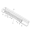
以下、本発明の実施形態を図面に基づいて説明する。図1に示すように、この実施形態の蛍光灯型LED灯具1は、天井や壁に取り付けられる長尺の灯具ボディ2を備えている。灯具ボディ2の両端には端板3が装着され、灯具ボディ2の下側に透光カバー4が取り付けられている。透光カバー4の内側において、灯具ボディ2の下面に光源基板5が設置され、光源基板5上に複数のLEDパッケージ6が一列に装着されている。そして、LEDパッケージ6が白色可視光を連続発光し、透光カバー4を通して室内の広範囲を照明するようになっている。
Hereinafter, embodiments of the present invention will be described with reference to the drawings. As shown in FIG. 1, a fluorescent lamp
図2に示すように、透光カバー4は光拡散グレード樹脂で成形され、内面に光拡散層8が塗装されている。灯具ボディ2は板金加工により中空管状に形成され、基板接合部9の両側縁に、透光カバー4の取付爪10が掛止される掛止穴11が形成されている。灯具ボディ2の左右両肩部は上向きの斜状に形成され、LEDパッケージ6の放射光の一部を灯具取付面12側に導く導光部13となっている。灯具ボディ2の内側には、ブラケット14を介して給電ユニット15が設置され、外部の交流商用電源を直流電圧に変換し、リード線16を介してLEDパッケージ6に供給する。
As shown in FIG. 2, the
図1、図2に示すように、光源基板5は長尺金属板で形成され、LEDパッケージ6が光源基板5とほぼ同じ長さで灯具ボディ2の長手方向に延びるように成形されている。LEDパッケージ6は、紫外または近紫外可視光を発生する複数のLEDチップ18と、各チップ18を連続的に封止する光透過性の封止部材19とを備えている。封止部材19は断面が半円形の帯状に成形され、透光性材料中に複数のチップ18をほぼ等間隔に封止している。なお、LEDパッケージ6は基板5と共に棒形の光源ユニットを構成し、灯具ボディ2の長さに応じた本数の光源ユニットが直列に接続されている。
As shown in FIGS. 1 and 2, the
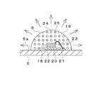
図3に示すように、光源基板5のチップ実装面5aにはAuメッキにより陽極20と陰極21が形成され、陽極20上にAgペースト22を介してLEDチップ18が実装されている。LEDチップ18には、380〜420nmの波長域に発光ピークを有する半導体発光素子が用いられ、その上面がAuワイヤ23を介して陰極21に接続されている。封止部材19は、透明シリコーン樹脂で光源基板5のチップ実装面5aから盛り上がるように成形されている。つまり、封止部材19は、底面がチップ実装面5aに接着され、底面を除く全表面が露出し、LEDパッケージ6が、チップ18の発光を封止部材19の表面全体から灯具ボディ2の側方域を含む広角に放射するように構成されている。
As shown in FIG. 3, an
また、封止部材19は、LEDチップ18が発した紫外または近紫外可視光を白色可視光に波長変換する2種類の蛍光体24,25を含有している。第1の蛍光体24は、LEDチップ18の発光を吸収し、560〜600nmの波長域にピーク波長を有する黄色系の可視光を発生する。第2の蛍光体25は、LEDチップ18の発光を吸収し、430〜480nmの波長域にピーク波長を有する青色系の可視光を発生する。第1、第2蛍光体24,25は、シリコーン樹脂中に均一な分布で分散し、補色の関係にある青色と黄色の混色によって、封止部材19の全表面からランバーシアンな白色可視光を発生する。
The sealing
第1の蛍光体24(黄色)には、例えば、次の一般式で表される組成物を使用できる。
一般式 (Ca1−x−y Srx Rey)7(SiO3)7X2
(ReはEu2+を必須とする希土類元素およびMn2+、XはCeを必須とするハロゲン元素である。)
For the first phosphor 24 (yellow), for example, a composition represented by the following general formula can be used.
General formula (Ca 1-xy Sr x Re y ) 7 (SiO 3 ) 7 X 2
(Re is a rare earth element essential for Eu 2+ and Mn 2+ , and X is a halogen element essential for Ce.)
第2の蛍光体25(青色)には、例えば、次の一般式で表される組成物を使用できる。
(1)一般式 M1 a(M2O4)bXc:Red
(M1は、Ca,Sr,Baのうち1種以上を必須とし、一部をMg,Zn,Cd,K,Ag,Tlからなる群の元素に置き換えることができる。M2は、Pを必須とし、一部をV,Si,As,Mn,Co,Cr,Mo,W,Bからなる群の元素に置き換えることができる。
Xは少なくとも1種のハロゲン元素、ReはEu2+を必須とする少なくとも1種の希土類元素またはMnを示す。aは4.2≦a≦5.8、bは2.5≦b≦3.5、cは0.8<c<1.4、dは0.01<d<0.1の範囲である。)
(2)一般式 M1 1−aMgAl10O17:Eu2+ a
(M1は、Ca,Sr,Ba,Znからなる群より選ばれる少なくとも1種の元素、aは0.001≦a≦0.5の範囲である。)
(3)一般式 M1 1−aMgSi2O8:Eu2+ a
(M1は、Ca,Sr,Ba,Znからなる群より選ばれる少なくとも1種の元素、aは0.001≦a≦0.8の範囲である。)
(4)一般式 M1 2−a(B5O9)X:Rea
(M1は、Ca,Sr,Ba,Znからなる群より選ばれる少なくとも1種の元素、Xは少なくとも1種のハロゲン元素、aは0.001≦a≦0.5の範囲である。)
For the second phosphor 25 (blue), for example, a composition represented by the following general formula can be used.
(1) General formula M 1 a (M 2 O 4 ) b X c: Re d
(M 1 is, Ca, Sr, an essential one or more of Ba, some Mg, Zn, Cd, K, Ag,
X represents at least one halogen element, and Re represents at least one rare earth element or Mn which essentially requires Eu 2+ . a is 4.2 ≦ a ≦ 5.8, b is 2.5 ≦ b ≦ 3.5, c is 0.8 <c <1.4, and d is in the range of 0.01 <d <0.1. is there. )
(2) General formula M 1 1-a MgAl 10 O 17 : Eu 2+ a
(M 1 is at least one element selected from the group consisting of Ca, Sr, Ba, and Zn, and a is in the range of 0.001 ≦ a ≦ 0.5.)
(3) General formula M 1 1-a MgSi 2 O 8 : Eu 2+ a
(M 1 is at least one element selected from the group consisting of Ca, Sr, Ba, and Zn, and a is in the range of 0.001 ≦ a ≦ 0.8.)
(4) General formula M 1 2-a (B 5 O 9 ) X: Re a
(M 1 is at least one element selected from the group consisting of Ca, Sr, Ba, and Zn, X is at least one halogen element, and a is in the range of 0.001 ≦ a ≦ 0.5.)
上記構成の蛍光灯型LED灯具1によれば、次のような作用効果が得られる。
(a)LEDパッケージ6を長尺に形成し、帯状の封止部材19で複数のLEDチップ18を連続的に封止したので、チップ18のツブツブ感をなくし、LEDパッケージ6を蛍光管のように連続的に発光させることができる。
(b)封止部材19を光源基板5のチップ実装面5aから盛り上がる形状に成形したので、LEDチップ18の発光を広角に分配し、灯具ボディ2の側方域への配光量を増やし、図4に示すように、放射角度90°地点の相対照度を0.4とすることができ、既存蛍光管とほぼ同等の配光パターンが得られる。
(c)また、灯具ボディ2の両肩部に導光部13を斜状に形成することで、LEDパッケージ6の放射光の一部を灯具取付面12側に導くことも可能となる。
According to the fluorescent lamp
(A) Since the
(B) Since the sealing
(C) In addition, by forming the
(d)封止部材19は、シリコーン樹脂中に青色発光の第1蛍光体24と黄色発光の第2蛍光体25を均一な分布で含有しているので、LEDチップ18が発生した紫外または近紫外光を白色可視光へ効率よく波長変換し、特に、灯具側方域における発光色の変動を抑え、均質な白色可視光で広範囲を明るく照明できる。
(e)また、上記波長域の蛍光体24,25は、黄色発光の第2蛍光体25が第1蛍光体24の青色光をほとんど吸収しないため、封止部材19を盛り上がり形状とした場合でも、多重励起(カスケード励起)による発光色の変動を抑制できるという利点もある。
(f)透光カバー4は、内面に光拡散層8が設けられているので、LEDパッケージ6の発光を効率よく透過して、LED灯具1の周囲へ均一に拡散できる。
(D) Since the sealing
(E) In addition, the
(F) Since the
本発明は、上記実施形態に限定されるものではなく、以下に例示するように、発明の趣旨を逸脱しない範囲で、各部の構成や形状を適宜に変更して実施することも可能である。
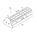
(1)図5に示すように、幅広の灯具ボディ32に光源基板5とLEDパッケージ6を2列または3列に並べ、広域照明用の蛍光灯型LED灯具31を構成すること。
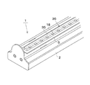
(2)図6に示すように、封止部材35を断面四角形の帯形に成形し、LEDパッケージ36を全体として角柱形に形成すること。
(3)その他、封止部材を断面三角形、台形、多角形など、各種の盛り上がり形状で成形すること。
The present invention is not limited to the above embodiment, and can be implemented by appropriately changing the configuration and shape of each part without departing from the spirit of the invention, as exemplified below.
(1) As shown in FIG. 5, the
(2) As shown in FIG. 6, the sealing
(3) In addition, the sealing member is molded in various raised shapes such as a cross-sectional triangle, trapezoid, and polygon.
1,31 蛍光灯型LED灯具
2,32 灯具ボディ
4 透光カバー
5 光源基板
5a チップ実装面
6,36 LEDパッケージ
8 光拡散層
15 給電ユニット
18 LEDチップ
19,35 封止部材
24,25 蛍光体
DESCRIPTION OF
Claims (5)
Priority Applications (2)
| Application Number | Priority Date | Filing Date | Title |
|---|---|---|---|
| JP2011055305A JP2012190744A (en) | 2011-03-14 | 2011-03-14 | Fluorescent lamp type led lamp |
| US13/419,861 US8746907B2 (en) | 2011-03-14 | 2012-03-14 | Fluorescent tube type LED lamp |
Applications Claiming Priority (1)
| Application Number | Priority Date | Filing Date | Title |
|---|---|---|---|
| JP2011055305A JP2012190744A (en) | 2011-03-14 | 2011-03-14 | Fluorescent lamp type led lamp |
Publications (1)
| Publication Number | Publication Date |
|---|---|
| JP2012190744A true JP2012190744A (en) | 2012-10-04 |
Family
ID=46828295
Family Applications (1)
| Application Number | Title | Priority Date | Filing Date |
|---|---|---|---|
| JP2011055305A Pending JP2012190744A (en) | 2011-03-14 | 2011-03-14 | Fluorescent lamp type led lamp |
Country Status (2)
| Country | Link |
|---|---|
| US (1) | US8746907B2 (en) |
| JP (1) | JP2012190744A (en) |
Cited By (2)
| Publication number | Priority date | Publication date | Assignee | Title |
|---|---|---|---|---|
| WO2014077631A1 (en) * | 2012-11-19 | 2014-05-22 | 서울반도체 주식회사 | Led lighting device |
| JP2014186966A (en) * | 2013-03-25 | 2014-10-02 | Panasonic Corp | Lighting fixture |
Families Citing this family (24)
| Publication number | Priority date | Publication date | Assignee | Title |
|---|---|---|---|---|
| US8118447B2 (en) | 2007-12-20 | 2012-02-21 | Altair Engineering, Inc. | LED lighting apparatus with swivel connection |
| US8360599B2 (en) | 2008-05-23 | 2013-01-29 | Ilumisys, Inc. | Electric shock resistant L.E.D. based light |
| US8901823B2 (en) | 2008-10-24 | 2014-12-02 | Ilumisys, Inc. | Light and light sensor |
| US8653984B2 (en) | 2008-10-24 | 2014-02-18 | Ilumisys, Inc. | Integration of LED lighting control with emergency notification systems |
| US8214084B2 (en) | 2008-10-24 | 2012-07-03 | Ilumisys, Inc. | Integration of LED lighting with building controls |
| US7938562B2 (en) | 2008-10-24 | 2011-05-10 | Altair Engineering, Inc. | Lighting including integral communication apparatus |
| US8324817B2 (en) | 2008-10-24 | 2012-12-04 | Ilumisys, Inc. | Light and light sensor |
| US8540401B2 (en) | 2010-03-26 | 2013-09-24 | Ilumisys, Inc. | LED bulb with internal heat dissipating structures |
| WO2011119921A2 (en) | 2010-03-26 | 2011-09-29 | Altair Engineering, Inc. | Led light with thermoelectric generator |
| US8523394B2 (en) | 2010-10-29 | 2013-09-03 | Ilumisys, Inc. | Mechanisms for reducing risk of shock during installation of light tube |
| WO2013028965A2 (en) | 2011-08-24 | 2013-02-28 | Ilumisys, Inc. | Circuit board mount for led light |
| KR20130078348A (en) * | 2011-12-30 | 2013-07-10 | 삼성전자주식회사 | Lighting device |
| US9184518B2 (en) | 2012-03-02 | 2015-11-10 | Ilumisys, Inc. | Electrical connector header for an LED-based light |
| US9163794B2 (en) | 2012-07-06 | 2015-10-20 | Ilumisys, Inc. | Power supply assembly for LED-based light tube |
| US9271367B2 (en) | 2012-07-09 | 2016-02-23 | Ilumisys, Inc. | System and method for controlling operation of an LED-based light |
| JP2014035826A (en) * | 2012-08-07 | 2014-02-24 | Toshiba Lighting & Technology Corp | Light source apparatus and lighting apparatus |
| US9285084B2 (en) | 2013-03-14 | 2016-03-15 | Ilumisys, Inc. | Diffusers for LED-based lights |
| US9267650B2 (en) | 2013-10-09 | 2016-02-23 | Ilumisys, Inc. | Lens for an LED-based light |
| CA2937642A1 (en) | 2014-01-22 | 2015-07-30 | Ilumisys, Inc. | Led-based light with addressed leds |
| US9702531B2 (en) | 2014-04-23 | 2017-07-11 | General Led, Inc. | Retrofit system and method for replacing linear fluorescent lamp with LED modules |
| US9510400B2 (en) | 2014-05-13 | 2016-11-29 | Ilumisys, Inc. | User input systems for an LED-based light |
| US10161568B2 (en) | 2015-06-01 | 2018-12-25 | Ilumisys, Inc. | LED-based light with canted outer walls |
| EP3196550B1 (en) * | 2016-01-20 | 2018-10-24 | OSRAM GmbH | A method of producing lighting devices and corresponding lighting device |
| WO2020114817A1 (en) * | 2018-12-04 | 2020-06-11 | Signify Holding B.V. | Light generating system comprising an elongated luminescent body |
Citations (10)
| Publication number | Priority date | Publication date | Assignee | Title |
|---|---|---|---|---|
| JP2002299697A (en) * | 2001-03-29 | 2002-10-11 | Mitsubishi Electric Lighting Corp | Led light-source device and illuminator |
| JP2003110150A (en) * | 2001-10-01 | 2003-04-11 | Matsushita Electric Ind Co Ltd | Semiconductor light-emitting element and light-emitting device using it |
| JP2008047851A (en) * | 2006-07-18 | 2008-02-28 | Nichia Chem Ind Ltd | Linear light emitting device and surface light emitting device using it |
| JP3142719U (en) * | 2008-03-13 | 2008-06-26 | 秀信 堀之内 | Fluorescent LED light |
| JP2009038348A (en) * | 2007-07-12 | 2009-02-19 | Koito Mfg Co Ltd | Light emitting device |
| JP2010067939A (en) * | 2008-08-12 | 2010-03-25 | Heiji Niiyama | Light-emitting device |
| JP2011014316A (en) * | 2009-06-30 | 2011-01-20 | Sharp Corp | Lighting device |
| JP2011032340A (en) * | 2009-07-31 | 2011-02-17 | Koito Mfg Co Ltd | Phosphor and light-emitting device |
| JP2011151059A (en) * | 2010-01-19 | 2011-08-04 | Heiji Niiyama | Light-emitting device |
| JP2012142167A (en) * | 2010-12-28 | 2012-07-26 | Panasonic Corp | Lamp and lighting system |
Family Cites Families (3)
| Publication number | Priority date | Publication date | Assignee | Title |
|---|---|---|---|---|
| JP2007122933A (en) | 2005-10-26 | 2007-05-17 | Matsushita Electric Works Ltd | Fluorescent lamp type led lamp |
| US20090140271A1 (en) * | 2007-11-30 | 2009-06-04 | Wen-Jyh Sah | Light emitting unit |
| US8382322B2 (en) | 2008-12-08 | 2013-02-26 | Avx Corporation | Two part surface mount LED strip connector and LED assembly |
-
2011
- 2011-03-14 JP JP2011055305A patent/JP2012190744A/en active Pending
-
2012
- 2012-03-14 US US13/419,861 patent/US8746907B2/en not_active Expired - Fee Related
Patent Citations (10)
| Publication number | Priority date | Publication date | Assignee | Title |
|---|---|---|---|---|
| JP2002299697A (en) * | 2001-03-29 | 2002-10-11 | Mitsubishi Electric Lighting Corp | Led light-source device and illuminator |
| JP2003110150A (en) * | 2001-10-01 | 2003-04-11 | Matsushita Electric Ind Co Ltd | Semiconductor light-emitting element and light-emitting device using it |
| JP2008047851A (en) * | 2006-07-18 | 2008-02-28 | Nichia Chem Ind Ltd | Linear light emitting device and surface light emitting device using it |
| JP2009038348A (en) * | 2007-07-12 | 2009-02-19 | Koito Mfg Co Ltd | Light emitting device |
| JP3142719U (en) * | 2008-03-13 | 2008-06-26 | 秀信 堀之内 | Fluorescent LED light |
| JP2010067939A (en) * | 2008-08-12 | 2010-03-25 | Heiji Niiyama | Light-emitting device |
| JP2011014316A (en) * | 2009-06-30 | 2011-01-20 | Sharp Corp | Lighting device |
| JP2011032340A (en) * | 2009-07-31 | 2011-02-17 | Koito Mfg Co Ltd | Phosphor and light-emitting device |
| JP2011151059A (en) * | 2010-01-19 | 2011-08-04 | Heiji Niiyama | Light-emitting device |
| JP2012142167A (en) * | 2010-12-28 | 2012-07-26 | Panasonic Corp | Lamp and lighting system |
Cited By (2)
| Publication number | Priority date | Publication date | Assignee | Title |
|---|---|---|---|---|
| WO2014077631A1 (en) * | 2012-11-19 | 2014-05-22 | 서울반도체 주식회사 | Led lighting device |
| JP2014186966A (en) * | 2013-03-25 | 2014-10-02 | Panasonic Corp | Lighting fixture |
Also Published As
| Publication number | Publication date |
|---|---|
| US8746907B2 (en) | 2014-06-10 |
| US20120236533A1 (en) | 2012-09-20 |
Similar Documents
| Publication | Publication Date | Title |
|---|---|---|
| JP2012190744A (en) | Fluorescent lamp type led lamp | |
| US9506632B2 (en) | Light-emitting module, and illumination light source and illumination device using same | |
| JP5826503B2 (en) | LED bulb | |
| US20140218908A1 (en) | Light-Emitting Device and Luminaire | |
| CA2765199A1 (en) | Led lamp with a wavelength converting layer | |
| US8956011B2 (en) | Bulb type semiconductor light-emitting device lamp | |
| JP2017163001A (en) | Light-emitting module and lighting device | |
| TW201535797A (en) | Light emitting device | |
| JP2016058614A (en) | Light emission device and luminaire | |
| JP6928823B2 (en) | Light emitting module and lighting equipment | |
| JP2010118531A (en) | White lighting system and lighting fixture for vehicle | |
| US8766536B2 (en) | Light-emitting module having light-emitting elements sealed with sealing member and luminaire having same | |
| JP5993497B2 (en) | LED lighting device | |
| JP2014082438A (en) | Light-emitting device and light device | |
| JP2011134902A (en) | Led light-emitting device | |
| JP2016167518A (en) | Light emission device and luminaire | |
| JP2006344617A (en) | Light-emitting device unit | |
| JP2015176949A (en) | Light emitting device, manufacturing method for the same, light source for illumination and lighting device | |
| JP2014044909A (en) | Straight pipe type lamp and lighting device | |
| JP2011171585A (en) | Light-emitting device | |
| JP6583572B2 (en) | Light emitting device | |
| JP2009071090A (en) | Light-emitting device | |
| JP2012204349A (en) | Light-emitting device | |
| JP2008244469A (en) | Light-emitting device | |
| JP2006147214A (en) | Lighting system |
Legal Events
| Date | Code | Title | Description |
|---|---|---|---|
| A621 | Written request for application examination |
Free format text: JAPANESE INTERMEDIATE CODE: A621 Effective date: 20140205 |
|
| A977 | Report on retrieval |
Free format text: JAPANESE INTERMEDIATE CODE: A971007 Effective date: 20140917 |
|
| A131 | Notification of reasons for refusal |
Free format text: JAPANESE INTERMEDIATE CODE: A131 Effective date: 20140930 |
|
| A521 | Written amendment |
Free format text: JAPANESE INTERMEDIATE CODE: A523 Effective date: 20141118 |
|
| A02 | Decision of refusal |
Free format text: JAPANESE INTERMEDIATE CODE: A02 Effective date: 20150106 |
|
| A521 | Written amendment |
Free format text: JAPANESE INTERMEDIATE CODE: A523 Effective date: 20150318 |
|
| A911 | Transfer to examiner for re-examination before appeal (zenchi) |
Free format text: JAPANESE INTERMEDIATE CODE: A911 Effective date: 20150408 |
|
| A912 | Re-examination (zenchi) completed and case transferred to appeal board |
Free format text: JAPANESE INTERMEDIATE CODE: A912 Effective date: 20150612 |