JP2012166380A - Substrate for mold, and method for inspecting the same - Google Patents
Substrate for mold, and method for inspecting the same Download PDFInfo
- Publication number
- JP2012166380A JP2012166380A JP2011027405A JP2011027405A JP2012166380A JP 2012166380 A JP2012166380 A JP 2012166380A JP 2011027405 A JP2011027405 A JP 2011027405A JP 2011027405 A JP2011027405 A JP 2011027405A JP 2012166380 A JP2012166380 A JP 2012166380A
- Authority
- JP
- Japan
- Prior art keywords
- substrate
- thickness
- less
- mold
- diameter
- Prior art date
- Legal status (The legal status is an assumption and is not a legal conclusion. Google has not performed a legal analysis and makes no representation as to the accuracy of the status listed.)
- Granted
Links
Images
Classifications
-
- G—PHYSICS
- G03—PHOTOGRAPHY; CINEMATOGRAPHY; ANALOGOUS TECHNIQUES USING WAVES OTHER THAN OPTICAL WAVES; ELECTROGRAPHY; HOLOGRAPHY
- G03F—PHOTOMECHANICAL PRODUCTION OF TEXTURED OR PATTERNED SURFACES, e.g. FOR PRINTING, FOR PROCESSING OF SEMICONDUCTOR DEVICES; MATERIALS THEREFOR; ORIGINALS THEREFOR; APPARATUS SPECIALLY ADAPTED THEREFOR
- G03F7/00—Photomechanical, e.g. photolithographic, production of textured or patterned surfaces, e.g. printing surfaces; Materials therefor, e.g. comprising photoresists; Apparatus specially adapted therefor
- G03F7/0002—Lithographic processes using patterning methods other than those involving the exposure to radiation, e.g. by stamping
-
- H10P76/204—
-
- B—PERFORMING OPERATIONS; TRANSPORTING
- B82—NANOTECHNOLOGY
- B82Y—SPECIFIC USES OR APPLICATIONS OF NANOSTRUCTURES; MEASUREMENT OR ANALYSIS OF NANOSTRUCTURES; MANUFACTURE OR TREATMENT OF NANOSTRUCTURES
- B82Y10/00—Nanotechnology for information processing, storage or transmission, e.g. quantum computing or single electron logic
-
- B—PERFORMING OPERATIONS; TRANSPORTING
- B82—NANOTECHNOLOGY
- B82Y—SPECIFIC USES OR APPLICATIONS OF NANOSTRUCTURES; MEASUREMENT OR ANALYSIS OF NANOSTRUCTURES; MANUFACTURE OR TREATMENT OF NANOSTRUCTURES
- B82Y40/00—Manufacture or treatment of nanostructures
-
- G—PHYSICS
- G03—PHOTOGRAPHY; CINEMATOGRAPHY; ANALOGOUS TECHNIQUES USING WAVES OTHER THAN OPTICAL WAVES; ELECTROGRAPHY; HOLOGRAPHY
- G03F—PHOTOMECHANICAL PRODUCTION OF TEXTURED OR PATTERNED SURFACES, e.g. FOR PRINTING, FOR PROCESSING OF SEMICONDUCTOR DEVICES; MATERIALS THEREFOR; ORIGINALS THEREFOR; APPARATUS SPECIALLY ADAPTED THEREFOR
- G03F1/00—Originals for photomechanical production of textured or patterned surfaces, e.g., masks, photo-masks, reticles; Mask blanks or pellicles therefor; Containers specially adapted therefor; Preparation thereof
- G03F1/60—Substrates
Landscapes
- Engineering & Computer Science (AREA)
- Nanotechnology (AREA)
- Chemical & Material Sciences (AREA)
- Physics & Mathematics (AREA)
- General Physics & Mathematics (AREA)
- Crystallography & Structural Chemistry (AREA)
- Condensed Matter Physics & Semiconductors (AREA)
- Manufacturing & Machinery (AREA)
- Mathematical Physics (AREA)
- Theoretical Computer Science (AREA)
- Exposure Of Semiconductors, Excluding Electron Or Ion Beam Exposure (AREA)
- Shaping Of Tube Ends By Bending Or Straightening (AREA)
- Moulds For Moulding Plastics Or The Like (AREA)
- Manufacturing Of Magnetic Record Carriers (AREA)
Abstract
【解決手段】表面に凹凸パターンが形成される直径が125〜300mmである円形状の金型用基板であって、該基板の直径125mm以下の円内の厚さばらつきが2μm以下である金型用基板。
【効果】表面に凹凸によるパターンが形成される円形状の金型用基板であって、上記基板の中心の直径125mm以下の円内の厚さばらつきが2μm以下である金型用基板を使用することによって、金型用基板上にパターンを作成するときと転写するときとでパターン位置が不整合になったり、パターン誤差が生じたりすることを防ぐことができ、高精細で複雑なパターンの転写が可能になる。
【選択図】図2A circular mold substrate having a concavo-convex pattern formed on a surface thereof having a diameter of 125 to 300 mm, wherein the thickness variation in a circle having a diameter of 125 mm or less is 2 μm or less. Substrate.
[Effect] Use is made of a circular mold substrate on the surface of which a pattern due to unevenness is formed, and the mold substrate has a thickness variation within 2 μm or less within a circle having a diameter of 125 mm or less at the center of the substrate. As a result, it is possible to prevent pattern positions from becoming inconsistent and pattern errors between when creating a pattern on a mold substrate and when transferring a pattern. Is possible.
[Selection] Figure 2
Description
本発明は、電子デバイス、光部品、記憶素子、バイオ素子等を製造する工程において、表面に凹凸形状を形成するための元板となる金型用基板及び金型用基板の検査方法に関する。 The present invention relates to a mold substrate serving as a base plate for forming an uneven shape on a surface and a method for inspecting a mold substrate in a process of manufacturing an electronic device, an optical component, a memory element, a bio element, and the like.
近年の電子デバイス、光部品、記憶素子、バイオ素子等の製造において、より一層の高性能化、高精細化が要求される一方で、製造の低コスト化も同時に要求される状況となっている。このような趨勢の中で、従来のリソグラフィ技術に比べ、安価に微細加工を行えるナノインプリント技術が注目されてきている。ナノインプリント技術において、凹凸パターンは機械的な方法により形成する。すなわち、所望の凹凸パターンを表面に作りこんだ金型を、所定の厚みの樹脂層を有する基板に押圧することで、金型の凹凸パターンを転写する。押圧により凹凸パターンが転写された樹脂層は硬化させることによりその形状が保存されるが、主に紫外線によって硬化させる方式と、熱によって硬化させる方式があり、いずれの方式においても金型と基板との平行度を保ち、押圧する面内を均一な圧力で押し付けることが重要である。
なお、本発明に関連する先行技術文献としては下記のものが挙げられる。
In the manufacture of electronic devices, optical components, memory elements, bio elements, etc. in recent years, while higher performance and higher definition are required, it is also required to reduce manufacturing costs at the same time. . In such a trend, nanoimprint technology capable of performing microfabrication at a low cost has attracted attention as compared with conventional lithography technology. In the nanoimprint technique, the concavo-convex pattern is formed by a mechanical method. That is, by pressing a mold having a desired concavo-convex pattern on its surface against a substrate having a resin layer having a predetermined thickness, the concavo-convex pattern of the mold is transferred. The shape of the resin layer to which the concavo-convex pattern has been transferred by pressing is cured to preserve its shape, but there are mainly a method of curing by ultraviolet rays and a method of curing by heat. It is important to keep the degree of parallelism and press the surface to be pressed with a uniform pressure.
In addition, the following are mentioned as prior art documents relevant to the present invention.
ナノインプリントに用いられる金型の外形は、例えば65mm角や152mm角の角形や、50φmm、100φmm、150φmm、200φmmの円形のもの等、用途に応じて様々な形状のものが使われている。一方、実質的に金型としての役割を担い、凹凸パターンを作り込む領域は外形に比べて小さい面積(概ね4000mm2以内)であることが多く、その領域は通常、基板の中心付近に形成される。一般的に、転写しようとするパターンが微細であるほど、パターンを形成するエリアが狭くなる傾向が見られる。 As the outer shape of the mold used for nanoimprint, various shapes such as 65 mm square, 152 mm square, and circular shapes of 50 mm, 100 mm, 150 mm, and 200 mm are used depending on applications. On the other hand, a region that substantially plays a role as a mold and forms a concavo-convex pattern is often a small area (approximately within 4000 mm 2 ) compared to the outer shape, and the region is usually formed near the center of the substrate. The In general, the finer the pattern to be transferred, the narrower the area for forming the pattern.
これはパターンが微細であればあるほど、上記の金型と基板の平行度や押圧の均一性に求められる精度が高くなるためであって、パターンが形成された面積が狭ければ、これらの精度を高めることができるからである。一方で、金型の外形がパターンの形成された領域に比べて大きい傾向があるのは、ナノインプリント用金型を作製するプロセスに理由を求めることができる。ナノインプリント用金型は、スパッタリングによるメタル膜の塗布工程、EB描画装置を用いたリソグラフィ工程、所望の微細パターンを転写した後のメタル層や基板表面のドライエッチング工程等を経て作製されるが、これら工程で使用される装置は、経済性や利便性の面から伝統的なリソグラフィ技術で使用してきた装置と共有されることが多い。それ故、これら装置に対応する基板のサイズも、必然的に伝統的なリソグラフィ技術で使用されてきた基板のサイズとなり、ナノインプリント用金型の外形サイズはパターンの形成された領域に比べて大きくなる傾向がある。 This is because the finer the pattern, the higher the accuracy required for the parallelism of the mold and the substrate and the uniformity of pressing, and if the area on which the pattern is formed is small, these This is because the accuracy can be increased. On the other hand, the reason that the outer shape of the mold tends to be larger than the region where the pattern is formed can be the reason for the process for producing the nanoimprint mold. The mold for nanoimprinting is manufactured through a metal film coating process by sputtering, a lithography process using an EB drawing apparatus, a metal layer after transferring a desired fine pattern, a dry etching process on the substrate surface, etc. An apparatus used in the process is often shared with an apparatus used in a traditional lithography technique in terms of economy and convenience. Therefore, the size of the substrate corresponding to these apparatuses is inevitably the size of the substrate used in the traditional lithography technique, and the outer size of the nanoimprint mold is larger than the area where the pattern is formed. Tend.
近年、紫外線を使ったナノインプリント等の、より高精細なパターンやより複雑なパターンを金型上に形成して転写する要求が高まってきている。このような経緯と、上述した理由から、金型用基板の平坦度、特にパターンが形成され、実質的に金型の役割を担う領域の平坦度は重要であり、転写するパターンが高精細で複雑であればあるほど、表面が十分平坦でないと、金型を製作するときと転写するときでパターン位置が不整合になったりパターン誤差が生じたりすることがあり問題になってきていた。 In recent years, there has been an increasing demand for forming and transferring higher-definition patterns and more complicated patterns such as nanoimprints using ultraviolet rays on a mold. For these reasons and the reasons described above, the flatness of the mold substrate, in particular, the pattern is formed, and the flatness of the region that substantially plays the role of the mold is important. The more complicated the surface, the less the surface is sufficiently flat, and this has been a problem because pattern positions may become misaligned and pattern errors may occur when the mold is manufactured and transferred.
本発明は、上記事情に鑑みなされたものであり、金型と基板との平行度を保ち、押圧する面内を均一な圧力で押し付けるために適した金型用基板及び金型用基板の検査方法を提供することを目的とする。 The present invention has been made in view of the above circumstances, and maintains the parallelism between the mold and the substrate, and is suitable for pressing the inside of the pressing surface with uniform pressure, and inspection of the mold substrate. It aims to provide a method.
本発明者らは、上記目的を達成するために鋭意検討した結果、円形状の金型用基板であって、凹凸パターンの形成される範囲である中心エリアの厚さのばらつき((厚さの最大値)−(厚さの最小値))が少ない金型用基板を用いることが、前記課題の解決に有用であることを見出し、本発明をなすに至ったものである。 As a result of intensive studies to achieve the above-mentioned object, the present inventors have found that a circular mold substrate has a thickness variation ((thickness It has been found that the use of a mold substrate having a minimum value (maximum value) − (minimum value of thickness)) is useful for solving the above problems, and has led to the present invention.
即ち、本発明は、以下の金型用基板及び金型用基板の検査方法を提供する。
請求項1:
表面に凹凸パターンが形成される直径が125〜300mmである円形状の金型用基板であって、該基板の直径125mm以下の円内の厚さばらつきが2μm以下であることを特徴とする金型用基板。
請求項2:
直径が300mm以下であって、全面の厚さばらつきが10μm以下であることを特徴とする請求項1記載の金型用基板。
請求項3:
前記直径125mm以下の円内において、最も板厚の厚い点tの板厚をT、中心cの板厚をC、tとcを結んだ直線と上記直径125mmの円の円周との交点のうち、tから遠い点eの板厚をEとしたとき、それぞれの板厚がT≧C≧Eの関係を満たすことを特徴とする請求項1又は2記載の金型用基板。
請求項4:
前記直径125mm以下の円内における板厚Tと板厚Eとが、0.6μm≧T−E≧0.3μmの関係を満たす請求項3記載の金型用基板。
請求項5:
石英ガラス基板であることを特徴とする請求項1〜4のいずれか1項記載の金型用基板。
請求項6:
転写パターンを形成するための金属薄膜又はレジスト膜を有する石英ガラス基板であることを特徴とする請求項1〜4のいずれか1項記載の金型用基板。
請求項7:
前記直径125mm以下の円内に存在する表面欠陥のサイズが0.5μm以下であることを特徴とする請求項1〜6のいずれか1項記載の金型用基板。
請求項8:
ナノインプリント用である請求項1〜7のいずれか1項記載の金型用基板。
請求項9:
請求項1〜8のいずれか1項記載の条件に当てはまる金型用基板か否かにより良否を判定することを特徴とする金型用基板の検査方法。
That is, the present invention provides the following mold substrate and mold substrate inspection method.
Claim 1:
A gold mold substrate having a diameter of 125 to 300 mm on which a concavo-convex pattern is formed on a surface thereof, wherein a thickness variation in a circle having a diameter of 125 mm or less is 2 μm or less Mold substrate.
Claim 2:
2. The mold substrate according to
Claim 3:
In the circle having a diameter of 125 mm or less, the thickness of the thickest point t is T, the thickness of the center c is C, the straight line connecting t and c and the circumference of the circle with the diameter of 125 mm. 3. The mold substrate according to
Claim 4:
The mold substrate according to
Claim 5:
The mold substrate according to any one of
Claim 6:
The mold substrate according to any one of
Claim 7:
The mold substrate according to any one of
Claim 8:
The mold substrate according to
Claim 9:
A method for inspecting a mold substrate, comprising: determining whether the substrate is a mold substrate that satisfies the condition according to any one of
本発明によれば、表面に凹凸によるパターンが形成される円形状の金型用基板であって、上記基板の中心の直径125mm以下の円内の厚さばらつきが2μm以下である金型用基板を使用することによって、金型用基板上にパターンを作製するときと転写するときとでパターン位置が不整合になったり、パターン誤差が生じたりすることを防ぐことができ、高精細で複雑なパターンの転写が可能になる。 According to the present invention, there is provided a mold substrate having a circular shape in which a pattern due to unevenness is formed on the surface, wherein the thickness variation in a circle having a diameter of 125 mm or less at the center of the substrate is 2 μm or less. By using the, it is possible to prevent the pattern position from becoming inconsistent and pattern error between the time of producing the pattern on the mold substrate and the time of transferring, and the high-definition and complicated Pattern transfer is possible.
本発明の金型用基板は、表面に凹凸パターンが形成される直径が125〜300mmの円形状の基板であって、この基板の直径125mm以下の円内の厚さばらつきが2μm以下であり、特にナノインプリント金型用の基板である。 The mold substrate of the present invention is a circular substrate having a diameter of 125 to 300 mm on which a concavo-convex pattern is formed on the surface, and the thickness variation in a circle having a diameter of 125 mm or less of this substrate is 2 μm or less, In particular, it is a substrate for a nanoimprint mold.
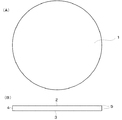
図1に、本発明に係る金型用基板を示す。図1(A)に示すように、基板1は、円形状の金型用の基板であり、図1(B)に示すように、上表面2、下表面3及び側面4で構成されている。通常、側面4と上表面2及び下表面3との境には、それぞれ面取り部5が形成されている。また、図示していないが、本発明の金型用基板の表面には、凹凸パターンを形成するための金属薄膜又はレジスト膜が予め成膜されていても良い。
FIG. 1 shows a mold substrate according to the present invention. As shown in FIG. 1A, the
本発明に係る金型用基板は、基板中心を中心とした直径125mm以下の円内の厚さばらつきが2μm以下、好ましくは1μm以下、更に好ましくは0.6μm以下である。2μmを超えるばらつき(平坦度)では、金型用の基板上にパターンを作製するときと、パターンを形成して得られた金型を転写するときとでパターン位置が不整合になったりパターン誤差が生じたりする。例えば、転写工程にて、所定の厚みの樹脂層を有する被転写用基板に押圧する際に、金型と被転写用基板との平行度が悪くなり、押圧する面内の圧力が均一ではなくなってしまう。この場合、金型を剥離した後の樹脂層の残膜厚が均一にならず、後工程であるドライエッチング工程やメタル膜の除去工程等全工程を通った後でも、所望のパターンが形成できていない結果となってしまう。なお、金型用基板の厚さのばらつきの下限値は特に制限されないが、小さい方が直径125mm以下の円内の厚さばらつきも小さくなる。また、金型用基板の厚さは、通常0.1〜30mm、特に0.5〜10mmであることが好ましい。上記ばらつきの規定範囲を直径125mm以下とするのは、ナノインプリント用基板において、工程全体を通した精度や効率の点から、一般的にパターンが形成される範囲がおおよそ125mm以下だからである。なお、厚さのばらつき(平坦度)は接触式の厚さ測定器で基板内の何点かを測る方法もあるが、光学干渉計やレーザー変位計等によってより精度よく測定することもできる。本発明においては、光学干渉式の平坦度測定装置((株)ニデック製FT90)により測定した値である。 The mold substrate according to the present invention has a thickness variation within a circle having a diameter of 125 mm or less around the center of the substrate of 2 μm or less, preferably 1 μm or less, more preferably 0.6 μm or less. When the variation (flatness) exceeds 2 μm, the pattern position becomes inconsistent or pattern error occurs when the pattern is formed on the mold substrate and when the mold obtained by forming the pattern is transferred. May occur. For example, when pressing a transfer substrate having a resin layer with a predetermined thickness in the transfer process, the parallelism between the mold and the transfer substrate deteriorates, and the pressure in the pressing surface is not uniform. End up. In this case, the residual film thickness of the resin layer after the mold is peeled off is not uniform, and a desired pattern can be formed even after passing through all processes such as a dry etching process and a metal film removing process which are subsequent processes. Results in not. The lower limit of the variation in the thickness of the mold substrate is not particularly limited, but the smaller the thickness, the smaller the variation in thickness within a circle having a diameter of 125 mm or less. Further, the thickness of the mold substrate is usually 0.1 to 30 mm, particularly preferably 0.5 to 10 mm. The reason why the prescribed range of the variation is set to 125 mm or less is that, in the nanoimprint substrate, the range in which a pattern is generally formed is approximately 125 mm or less from the viewpoint of accuracy and efficiency throughout the entire process. Although there is a method of measuring the thickness variation (flatness) at several points in the substrate with a contact-type thickness measuring device, it can also be measured more accurately with an optical interferometer, a laser displacement meter, or the like. In the present invention, it is a value measured by an optical interference type flatness measuring device (FT90 manufactured by Nidec Co., Ltd.).
金型用基板の直径は、扱いやすさから300mm以下、特に125〜200mmであることが多く、この場合、基板全体の厚さばらつきが大きいと125mm以下の円内の厚さばらつきを小さくすることが難しく、更にパターン形成部より外の領域であっても厚さばらつきが大きいと転写の精度に影響を与えてしまうので、基板全面の厚さばらつきが10μm以下であることが好ましく、更に好ましくは5μm以下である。下限値は特に制限されず、小さければ小さいほどよい。全面の厚さばらつきの範囲を厳密に規定するならば、実質的に精度よく測定できる範囲、すなわち、周縁から3mm内側の円形範囲となる。周縁から3mmまでの範囲は、面取り部に近いことから、接触式の厚さ測定器では、測定器の厚さ測定部位の面積が広いため、一部面取り部にかかってしまい、厚さを正確に測定できない場合がある。光学干渉計やレーザー変位計であっても、周辺から3mmまでの範囲は、端面や面取り部が近いために散乱光の影響によって正確に測定できない場合がある。
The diameter of the mold substrate is often 300 mm or less, particularly 125 to 200 mm for ease of handling. In this case, if the thickness variation of the whole substrate is large, the thickness variation in a circle of 125 mm or less should be reduced. Further, even if the thickness variation is large even in the region outside the pattern forming portion, the transfer accuracy is affected. Therefore, the thickness variation on the entire surface of the substrate is preferably 10 μm or less, and more preferably. 5 μm or less. The lower limit is not particularly limited, and the lower the better, the better. If the range of variation in the thickness of the entire surface is strictly defined, it becomes a range that can be measured substantially accurately, that is, a
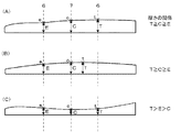
更に、図2(A),(B)に示すように、本発明に係る金型用基板の中心の直径125mm以下の円内において、最も板厚の厚い点tの板厚をT、中心cの板厚をC、tとcを結んだ直線と直径125mmの円の円周との交点のうち、tから遠い点eの板厚をEとしたとき、それぞれの板厚を比較してT≧C≧Eの関係を満たすことが好ましい。なお、図中、6の破線は直径125mmの円の円周の位置を示し、7の破線は基板(及び直径125mmの円)の中心を示す。 Further, as shown in FIGS. 2A and 2B, the thickness of the thickest point t is T and the center c in a circle having a diameter of 125 mm or less at the center of the mold substrate according to the present invention. Of the intersection of the straight line connecting C, t and c and the circumference of a circle with a diameter of 125 mm, where E is the thickness of the point e far from t, It is preferable to satisfy the relationship of ≧ C ≧ E. In the figure, a broken line 6 indicates the position of the circumference of a circle having a diameter of 125 mm, and a broken line 7 indicates the center of the substrate (and a circle having a diameter of 125 mm).
金型の転写工程は、転写するパターンが微細であるため、パターンの間に気泡が入って、転写後のパターンに欠陥が生じてしまうことがある。これを避けるために、装置側では、転写工程を真空に近い雰囲気で行うよう工夫している場合もあるが、それでも完全な真空雰囲気ではないために気泡による欠陥が完全になくなっているわけではない。金型用基板の板厚においてT≧C≧Eの関係を満たすような形状にしておけば、このような転写工程時で発生する気泡による欠陥を軽減することができる。つまり、T≧C≧Eの関係を満たす場合、転写の際に、金型の表面のうち、最初に基板の樹脂層と接する部位は板厚が最も厚いTの部分であり、最後に基板の樹脂層と接する部位はEの部分となる。Eはパターンの形成された領域の端であるため、たとえ樹脂中に気泡や異物があったとしても、それらはパターンの形成された領域の外側へ逃げて、転写されたパターンに影響を与えない可能性が高くなる。一方、仮に図2(C)のようにT>E>Cの関係を満たすような形状であった場合、金型の表面のうち、最後に基板の樹脂層と接する部位はCとなる。この場合、樹脂層の中に気泡や異物があると、それらがパターンの形成された領域の中心付近に集まってしまい、転写されたパターンに欠陥が生じてしまうおそれがある。 In the transfer process of the mold, since the pattern to be transferred is fine, bubbles may enter between the patterns, resulting in defects in the transferred pattern. In order to avoid this, the device side may devise to perform the transfer process in an atmosphere close to a vacuum. However, since it is not a complete vacuum atmosphere, defects due to bubbles are not completely eliminated. . If a shape satisfying the relationship of T ≧ C ≧ E in the thickness of the mold substrate is used, defects due to bubbles generated during such a transfer process can be reduced. That is, when the relationship of T ≧ C ≧ E is satisfied, the portion of the mold surface that comes into contact with the resin layer of the substrate first at the time of transfer is the portion of T with the largest plate thickness, and finally the substrate surface. A portion in contact with the resin layer is an E portion. Since E is the edge of the area where the pattern is formed, even if there are bubbles or foreign matter in the resin, they escape outside the area where the pattern is formed and do not affect the transferred pattern. The possibility increases. On the other hand, if the shape satisfies the relationship of T> E> C as shown in FIG. 2C, the portion of the mold surface that comes into contact with the resin layer of the substrate is C. In this case, if there are bubbles or foreign substances in the resin layer, they may gather near the center of the area where the pattern is formed, and the transferred pattern may be defective.
前述のT≧C≧Eの関係を満たすような形状の基板において、Tの板厚とEの板厚にある程度差があった場合には、より気泡や異物が抜けやすく、パターン上の欠陥を防ぐ効果が期待できる。具体的には0.6μm≧T−E≧0.3μmの関係を満たしていることが好ましい。より好ましくは0.4μm≧T−E≧0.3μmである。この値が0.6μmより大きいと、板厚ばらつきが0.6μmより大きいことになり、金型用の基板上にパターンを作製するときと転写するときとでパターン位置が不整合になりやすく、パターン誤差が生じやすい可能性がある。0.3μmよりも小さいと、気泡や異物が外側に逃げるのに板厚の差が十分でなく、それらがパターンの形成された領域の中心付近に集まってしまい、T≧C≧Eの関係を満たしていても、転写されたパターンに欠陥が生じる可能性がある。 In a substrate having a shape satisfying the above-described relationship T ≧ C ≧ E, if there is a difference between the thickness of T and the thickness of E to some extent, bubbles and foreign matters are more likely to escape, and defects on the pattern are eliminated. The effect to prevent can be expected. Specifically, it is preferable that the relationship of 0.6 μm ≧ TE−0.3 μm is satisfied. More preferably, 0.4 μm ≧ TE ≧ 0.3 μm. If this value is larger than 0.6 μm, the plate thickness variation is larger than 0.6 μm, and the pattern position tends to be inconsistent between when the pattern is formed on the mold substrate and when the pattern is transferred. Pattern errors can easily occur. If it is smaller than 0.3 μm, the difference in plate thickness is not enough for bubbles and foreign matters to escape to the outside, and they gather near the center of the area where the pattern is formed, and the relationship of T ≧ C ≧ E is satisfied. Even if it is satisfied, the transferred pattern may be defective.
ここで、本発明の金型用基板は石英ガラス基板であることが好ましい。石英ガラス基板は紫外線を透過する性質から、樹脂層を硬化させるために紫外線を利用するナノインプリントに利用されることが多い。樹脂層を硬化させるために熱を利用するナノインプリントの方式もあるが、この方式では熱膨張の影響を受けるため、紫外線を利用する方式の方がより微細なパターンの転写に向いているといわれている。また、石英ガラスは可視光領域においても透明であるために、転写の際の位置合わせもしやすいという利点もある。石英ガラス以外のナノインプリント用の金型用基板としては、シリコン(Si)、シリコン酸化膜、ポリジメチルシロキサン(PDMS)、ニッケル(Ni)、サファイアや、これらのハイブリッド素材等が挙げられる。 Here, the mold substrate of the present invention is preferably a quartz glass substrate. Quartz glass substrates are often used for nanoimprints that use ultraviolet light to cure the resin layer because of the property of transmitting ultraviolet light. There is also a nanoimprint method that uses heat to cure the resin layer, but because this method is affected by thermal expansion, it is said that the method using ultraviolet rays is more suitable for transferring finer patterns. Yes. In addition, since quartz glass is transparent even in the visible light region, there is an advantage that it is easy to align during transfer. Examples of the mold substrate for nanoimprinting other than quartz glass include silicon (Si), silicon oxide film, polydimethylsiloxane (PDMS), nickel (Ni), sapphire, and hybrid materials thereof.
本発明の金型用基板は、転写パターンを形成するための金属薄膜又はレジスト膜を有していてもよい。金型基板にパターンを形成する際にはEB描画装置を用いるが、その前に金属薄膜やレジスト膜を塗布しておくことが好ましい。金属薄膜又はレジスト膜は、常法に従い5nm〜5μmの厚さの膜を形成することができる。この場合、このような膜を形成させた状態で板厚を測定して、上述したように、中心の直径125mm以下の円の範囲の厚さばらつきが2μm以下であることが好ましい。 The mold substrate of the present invention may have a metal thin film or a resist film for forming a transfer pattern. When a pattern is formed on the mold substrate, an EB drawing apparatus is used, but it is preferable to apply a metal thin film or a resist film before that. As the metal thin film or resist film, a film having a thickness of 5 nm to 5 μm can be formed according to a conventional method. In this case, the plate thickness is measured in a state where such a film is formed, and as described above, it is preferable that the thickness variation in the range of the circle having a center diameter of 125 mm or less is 2 μm or less.
本発明の金型用基板において、直径125mm以下の円内の表面欠陥のサイズは0.5μm以下が好ましく、より好ましくは0.25μm以下であり、更に好ましくは0.1μm以下である。金型用基板の表面にはサブミクロンからナノオーダーの微細なパターンが形成されるので、金型用基板の表面に欠陥があると、欠陥がその大きさのまま被転写側の基板にも転写されてしまうためである。なお、本発明において、表面欠陥のサイズは、原子間力顕微鏡(Atomic Force Microscope:AFM)により測定した値である。 In the mold substrate of the present invention, the size of surface defects in a circle having a diameter of 125 mm or less is preferably 0.5 μm or less, more preferably 0.25 μm or less, and further preferably 0.1 μm or less. Since a fine pattern of sub-micron to nano order is formed on the surface of the mold substrate, if there is a defect on the surface of the mold substrate, the defect is transferred to the substrate on the transfer side as it is. It is because it will be done. In the present invention, the size of the surface defect is a value measured by an atomic force microscope (AFM).
本発明の金型用基板は、中心の直径125mm以内の範囲の厚さばらつきが2μm以下になるように基板の表裏面を研磨することで得ることができる。この場合の研磨方法は、研磨砥粒を含有した研磨液を供給しながら、両面研磨機を用いて表裏面を同時に研磨しても良いし、片面研磨機を用いて片面ずつ研磨することもできる。また、片面研磨においては基板よりも大きな研磨定盤を使っても良いし、基板よりも小さな定盤を用いることもできる。合成石英ガラス基板の場合、合成石英原料を常法に従いスライス、ラッピングしたものを用いることができる。 The mold substrate of the present invention can be obtained by polishing the front and back surfaces of the substrate so that the thickness variation within the central diameter of 125 mm is 2 μm or less. In this case, the polishing method may be such that the front and back surfaces are simultaneously polished using a double-side polishing machine while supplying a polishing liquid containing polishing abrasive grains, or each side can be polished using a single-side polishing machine. . In single-side polishing, a polishing platen larger than the substrate may be used, or a platen smaller than the substrate may be used. In the case of a synthetic quartz glass substrate, a synthetic quartz raw material sliced and lapped according to a conventional method can be used.
ここで、金型用基板の表面形状を所望の厚さばらつきの範囲内につくりこむためには、最終精密研磨工程前の粗研磨工程が重要となる。例えば、粗研磨工程では両面研磨機を用いて基板の表裏面を同時に加工する方法があるが、このとき、それぞれ研磨布を貼り付けた上定盤と下定盤の平坦度がより高い方が好ましい。研磨布としては、硬質発泡ポリウレタン等を用いることができるが、常に研磨布表面の平坦度を高く保つため、数バッチ毎にペレット修正を行うことも有効である。ペレット修正は、ダイヤモンドペレット付修正キャリア等の修正キャリアを用いて水又は砥粒を掛け流しながら、釣り合い圧から30gf/cm2の荷重を加えつつ、数分〜数十分程度、通常の研磨と同じ要領で、所定の研磨機のギアにはまるように設計した修正キャリアを仕掛けて研磨布表面平坦度修正を施すことが好ましい。 Here, in order to produce the surface shape of the mold substrate within a desired thickness variation range, a rough polishing step before the final precision polishing step is important. For example, in the rough polishing process, there is a method of simultaneously processing the front and back surfaces of the substrate using a double-side polishing machine. At this time, it is preferable that the flatness of the upper surface plate and the lower surface plate to which the polishing cloth is attached is higher. . As the polishing cloth, hard foamed polyurethane or the like can be used. However, in order to always keep the flatness of the polishing cloth surface high, it is also effective to perform pellet correction every several batches. Pellet correction is performed with normal polishing for several minutes to several tens of minutes while applying a load of 30 gf / cm 2 from the balance pressure while pouring water or abrasive grains using a correction carrier such as a correction carrier with diamond pellets. In the same manner, it is preferable to apply a correction carrier designed to fit into a gear of a predetermined polishing machine to correct the surface flatness of the polishing cloth.
粗研磨工程で一般的に使用される硬質発泡ポリウレタン研磨布に関しては、研磨液が基板全体に行き渡るように溝を形成しておくことが好ましい。研磨液が基板全体に行き渡ることによって、面内の研磨むらが少なくなり、厚さばらつきの少ない基板が得られる。研磨布の溝の形状は、多数の実条又は凹溝が互いに所定間隔をおいて平行に形成された条理状等とすることができる。 With respect to the hard foam polyurethane polishing cloth generally used in the rough polishing step, it is preferable to form grooves so that the polishing liquid spreads over the entire substrate. By spreading the polishing liquid over the entire substrate, in-plane polishing unevenness is reduced, and a substrate with less thickness variation can be obtained. The shape of the groove of the polishing cloth can be a stripe or the like in which a large number of actual strips or concave grooves are formed in parallel with each other at a predetermined interval.
粗研磨に用いる研磨液としては、シリカ、セリア、アランダム、ホワイトアランダム(WA)、FO、ジルコニア、SiC、ダイヤモンド、チタニア、ゲルマニア等の研磨砥粒を含むものが挙げられ、砥粒の粒度は0.1〜10μm、特に0.5〜3μmが好ましく、研磨液としては、これらの水スラリー等を好適に用いることができる。 Examples of the polishing liquid used for rough polishing include those containing abrasive grains such as silica, ceria, alundum, white alundum (WA), FO, zirconia, SiC, diamond, titania, germania, and the like. Is preferably 0.1 to 10 μm, particularly preferably 0.5 to 3 μm. As the polishing liquid, these water slurries can be suitably used.
最終精密研磨後に、中心の直径125mm以内の範囲において、最も板厚の厚い点tの板厚をT、中心点cの板厚をC、tとcを結んだ直線と中心の直径125mmの円周との交点のうち、tから遠い点eの板厚をEとしたとき、T≧C≧Eとなる板厚の関係を満たした形状を狙う場合、粗研磨工程での表面形状制御が重要となる。しかし、上記手法以外にも、例えば、両面研磨機の自公転比を制御したり、研磨キャリアのワークをセットするホールの位置、即ちキャリアの中心とホールの中心の変位を適切に選定することによって基板表面形状を制御できる。このような形状の制御を行うためには、ラップ加工後と粗研磨後に厚さばらつきや形状を確認することが好ましい。確認の方法としては、光学干渉計やレーザー変位計を用いて測定しても良いが、本発明においては、光学干渉計を用いて測定する。 After the final precision polishing, within the range of the center diameter within 125mm, the thickness of the thickest point t is T, the thickness of the center point c is C, the straight line connecting t and c and the circle with the center diameter of 125mm When the thickness of a point e far from t of the intersections with the circumference is E, when aiming for a shape satisfying the relationship of the thickness of T ≧ C ≧ E, it is important to control the surface shape in the rough polishing process It becomes. However, in addition to the above method, for example, by controlling the revolution ratio of the double-side polishing machine, or by appropriately selecting the position of the hole where the workpiece of the polishing carrier is set, that is, the displacement between the center of the carrier and the center of the hole The substrate surface shape can be controlled. In order to control such a shape, it is preferable to check thickness variations and shapes after lapping and rough polishing. As a confirmation method, measurement may be performed using an optical interferometer or a laser displacement meter. However, in the present invention, measurement is performed using an optical interferometer.
粗研磨工程終了時点の形状として、その後、最終精密研磨することによって、所定の厚さばらつきの範囲に入りながら、T≧C≧Eとなる板厚の関係を満たす形状になることが好ましい。具体的には、粗研磨工程終了時点で、C,Eの関係において、C≧Eの場合、中心の直径125mm以内の範囲の厚さばらつきが1.5μm以下、特に0〜1.0μmであることが好ましい。この厚さばらつきが大きすぎると最終研磨工程では基板の中心よりも端の研磨量が多くなる傾向があるので、この場合は、最終研磨工程後に直径125mm以内の範囲の厚さばらつきが2μm以内に入ってこない場合がある。また、EとCの厚さの差が0.1μm程度でほぼ同一か、もしくはE>Cの場合、中心の直径125mm以内の範囲の厚さばらつきが2μm以下、特に0〜1.5μmであることが好ましい。この厚さばらつきが大きすぎると、最終研磨工程では基板中心よりも端の研磨量が多くなる傾向にあるので、最終研磨によって基本的厚さばらつきはほぼ変わらないか、もしくは縮小していく傾向となる。そのため、粗研磨上がりの形状でC>Eの場合よりも厚さばらつき許容値は大きいが、大きすぎると最終研磨工程後に直径125mm以内の範囲の厚さばらつきが2μm以内に入らない場合がある。前述の通り、最終精密研磨工程では、基板の中心よりも端の研磨量が多くなる傾向があるので、最終研磨工程後に厚さばらつきを小さくするには、粗研磨終了時点でCの厚さとEの厚さがほぼ同一か、もしくはE>Cの関係を満たしていた方が有利である。 The shape at the end of the rough polishing step is preferably a shape that satisfies the relationship of thickness of T ≧ C ≧ E while entering the range of a predetermined thickness variation by performing final precision polishing thereafter. Specifically, at the end of the rough polishing step, in the relationship between C and E, when C ≧ E, the thickness variation within the central diameter of 125 mm is 1.5 μm or less, particularly 0 to 1.0 μm. It is preferable. If the thickness variation is too large, the amount of polishing at the end is larger than the center of the substrate in the final polishing step. In this case, the thickness variation within a diameter of 125 mm after the final polishing step is within 2 μm. It may not come in. In addition, when the difference between the thicknesses of E and C is approximately the same at about 0.1 μm, or when E> C, the thickness variation within the central diameter of 125 mm is 2 μm or less, particularly 0 to 1.5 μm. It is preferable. If this thickness variation is too large, the polishing amount at the edge tends to be larger than the center of the substrate in the final polishing step, so the basic thickness variation will not change or be reduced by the final polishing. Become. For this reason, the thickness variation tolerance is larger than the case of C> E in the shape of rough polishing, but if it is too large, the thickness variation within the range of 125 mm in diameter may not be within 2 μm after the final polishing step. As described above, in the final precision polishing process, the amount of polishing at the edge tends to be larger than the center of the substrate. Therefore, in order to reduce the thickness variation after the final polishing process, the thickness of C and E at the end of rough polishing are reduced. It is advantageous that the thicknesses of these are substantially the same or satisfy the relationship of E> C.
粗研磨工程が終了した後、最終精密研磨工程において使用する研磨布は、必要な表面の品質に応じて任意に選ぶことができるが、例えば、スウェード、ウレタン含浸不織布、軟質の発泡ウレタン等の材質のものを用いることができる。基板全体にわたって研磨液が均一に供給されなかったり、削られた屑が速やかに排出されないで研磨布内に詰まったりすると、基板内で研磨速度に不均一が生じて、結果として厚さばらつきが大きくなることがある。これを避けるために、研磨布には全面に溝を形成すると良い。この溝によって研磨液が均一に供給されて基板内部に十分に研磨液がいきわたり、かつ、削りかすがこの溝を通って速やかに排出されるため、研磨速度が制御可能となって厚さばらつきをよくすることができる。溝の形状は、条理状等とすることができる。 After the rough polishing process is finished, the polishing cloth used in the final precision polishing process can be arbitrarily selected according to the required surface quality. For example, materials such as suede, urethane-impregnated nonwoven fabric, soft urethane foam, etc. Can be used. If the polishing liquid is not supplied uniformly over the entire substrate, or if scraped scraps are not quickly discharged and become clogged in the polishing cloth, the polishing rate will be uneven within the substrate, resulting in large thickness variations. May be. In order to avoid this, it is preferable to form grooves on the entire surface of the polishing cloth. The polishing liquid is uniformly supplied by this groove, and the polishing liquid sufficiently flows inside the substrate, and the shavings are quickly discharged through this groove, so that the polishing speed can be controlled and the thickness variation is improved. can do. The shape of the groove can be a stripe or the like.
研磨液に含まれる研磨砥粒としては、シリカ、セリア、アランダム、ホワイトアランダム(WA)、FO、ジルコニア、SiC、ダイヤモンド、チタニア、ゲルマニア等が挙げられ、その粒度は5〜1,000nm、特に10〜150nmが好ましく、研磨液としては、これらの水スラリー等を好適に用いることができる。 Examples of the abrasive grains contained in the polishing liquid include silica, ceria, alundum, white alundum (WA), FO, zirconia, SiC, diamond, titania, germania, and the particle size is 5 to 1,000 nm. In particular, a thickness of 10 to 150 nm is preferable, and these water slurries and the like can be suitably used as the polishing liquid.
それでも板厚ばらつきが所望の範囲に入らない場合や、形成するパターンが微細であって特に小さな板厚ばらつきが求められる場合は、板厚の高い部分を狙って平坦化するプラズマエッチング技術や、部分小型研磨ツール等を用いた研磨技術を用いて板厚ばらつきを小さくしてもよい。このような部分研磨方法は、例えば特開2002−318450号公報に記載されている。 If the plate thickness variation still does not fall within the desired range, or if the pattern to be formed is fine and particularly small plate thickness variation is required, plasma etching technology for flattening the portion with a high plate thickness The plate thickness variation may be reduced by using a polishing technique using a small polishing tool or the like. Such a partial polishing method is described in, for example, JP-A-2002-318450.
本発明の金型用基板の検査方法は、上記条件に当てはまる金型用基板か否かを例えば光学干渉式の平坦度測定装置によって厚さばらつきを測定することにより判断し、基板の良否を判定することにより行うことができる。 In the method for inspecting a mold substrate according to the present invention, it is determined whether or not the mold substrate satisfies the above conditions by measuring thickness variation using, for example, an optical interference type flatness measuring device, and determining whether the substrate is good or bad. This can be done.
以下、実施例及び比較例を示して本発明を具体的に説明するが、本発明は下記の実施例に制限されるものではない。 EXAMPLES Hereinafter, although an Example and a comparative example are shown and this invention is demonstrated concretely, this invention is not restrict | limited to the following Example.
[実施例1]
合成石英原料をスライス、ラッピング加工を行い、直径約6インチ、板厚1.0mmのすりガラス面のウェーハ中間原料を得た。これを比較的粒度の粗い酸化セリウム系研磨剤(平均粒径1.4μm;商品名SHOROX、昭和電工(株)製)と硬質発泡ポリウレタンを組み合わせた粗研磨工程に投入した。粗研磨は両面研磨機を用いて行い、硬質発泡ポリウレタンの研磨布表面には条理状に溝(溝ピッチ3cm、溝幅2mm)を形成し、所定のバッチ毎にダイヤモンドペレット修正を行うなどしてウェーハが所望の厚さばらつきと形状になるよう、研磨布面の制御を行った。
[Example 1]
A synthetic quartz raw material was sliced and lapped to obtain a wafer intermediate raw material with a ground glass surface having a diameter of about 6 inches and a plate thickness of 1.0 mm. This was put into a coarse polishing step in which a relatively coarse cerium oxide-based abrasive (average particle size 1.4 μm; trade name SHOROX, Showa Denko KK) and hard polyurethane foam were combined. Rough polishing is performed by using a double-side polishing machine, and the surface of the hard foamed polyurethane polishing cloth is formed with a streak-like groove (
その結果、粗研磨上がりで厚さ約0.5mmの設定通りのおおむね凸形状のウェーハ基板に仕上がった。光学干渉式の平坦度測定装置(ニデック社製FT90)を用い、基板中心部の直径125mm以内の範囲において、最も板厚の厚い点tの板厚をT、中心点cの板厚をC、tとcを結んだ直線と中心の直径125mmの円周との交点のうち、tから遠い点eの板厚をEとしたとき、粗研磨上がりの状態での板厚の関係はC>Eを満たしており、中心の直径125mm以内の範囲の厚さばらつき「(基板厚さの最大値)−(基板厚さの最小値)」は0.3μmであった。 As a result, it was finished into a roughly convex wafer substrate as set with a thickness of about 0.5 mm after rough polishing. Using an optical interference type flatness measuring device (FT90 manufactured by Nidec Co., Ltd.), the thickness of the thickest point t is T, and the thickness of the central point c is C, within the range of the diameter of the central part of the substrate within 125 mm. Of the intersections between the straight line connecting t and c and the circumference with a diameter of 125 mm at the center, when the plate thickness at a point e far from t is E, the relationship between the plate thicknesses after rough polishing is C> E. The thickness variation “(maximum value of substrate thickness) − (minimum value of substrate thickness)” in the range of the central diameter within 125 mm was 0.3 μm.
次に、この基板を精密研磨によって平滑鏡面化を行った。両面研磨機にスェード製の研磨布で条理状に溝(溝ピッチ3cm)を形成したものを貼り、酸化セリウム系研磨砥粒を含む研磨液(平均粒径0.8μm;商品名ミレーク、三井金属鉱業(株)製)を供給しながら研磨を行った。研磨終了後に基板を精密洗浄し、乾燥してから基板の厚さばらつきを調べた。光学干渉式の平坦度測定装置(ニデック社製FT90)で中心部直径125mm領域における厚さばらつきを測定したところ、「(基板厚さの最大値)−(基板厚さの最小値)」は0.6μmと非常に小さい値を示した。全面の板厚ばらつきを測定したところ2.1μmであった。その形状は中心板厚が最も厚く、おおむね凸形状であった。T、C、Eの関係を調べたところ、T−E=0.6μmであり、T≧C≧Eの関係を満たしていたので、この基板は合格品として取得した。なお、中心部直径125mmの領域における表面欠陥のサイズは0.25μm以下であった。
Next, this substrate was made into a smooth mirror surface by precision polishing. A double-side polishing machine with a suede polishing cloth with grooves (
[実施例2]
実施例1と同様の方法で原料基板を用意し、粗研磨まで行った。C,Eの関係を調べたところ、粗研磨上がりの状態での板厚の関係は、C>Eを満たしており、中心の直径125mm以内の範囲の厚さばらつきは1.2μmであった。その後、実施例1と同様に精密研磨を行い、更に小型の研磨ツールにて、凸形状であった中心付近を狙って研磨することで中心の板厚を落とした。
このようにして作製した基板の厚さばらつきを測定したところ、中心部直径125mm領域における厚さばらつきは0.3μmと非常に小さい値を示した。また、全面の板厚ばらつきを測定したところ1.8μmであった。その形状は台形状で中心付近一帯の板厚がほぼ均一で、外周に比べて厚かった。T、C、Eの関係を調べたところ、T−E=0.3μmであり、T≧C≧Eを満たしていたので、この基板は合格品として取得した。なお、中心部直径125mmの領域における表面欠陥のサイズは0.25μm以下であった。
[Example 2]
A raw material substrate was prepared in the same manner as in Example 1 and was subjected to rough polishing. When the relation between C and E was examined, the relation of the plate thickness in the state of rough polishing was such that C> E, and the thickness variation within the central diameter of 125 mm was 1.2 μm. Thereafter, precision polishing was performed in the same manner as in Example 1, and the center plate thickness was reduced by polishing with a small polishing tool aiming at the vicinity of the convex center.
When the thickness variation of the substrate thus produced was measured, the thickness variation in the region of the central part diameter of 125 mm showed a very small value of 0.3 μm. Further, the thickness variation of the entire surface was measured and found to be 1.8 μm. Its shape was trapezoidal, and the plate thickness around the center was almost uniform and thicker than the outer periphery. When the relationship between T, C, and E was examined, T−E = 0.3 μm and T ≧ C ≧ E was satisfied, so this substrate was obtained as an acceptable product. In addition, the size of the surface defect in the region having a central part diameter of 125 mm was 0.25 μm or less.
[実施例3]
実施例1と同様の方法で原料基板を用意し、粗研磨まで行った。C,Eの関係を調べたところ、粗研磨上がりの状態での板厚の関係は、C>Eを満たしており、中心の直径125mm以内の範囲の厚さばらつきは1.2μmであった。その後、実施例1と同様に精密研磨を行った。ただし、精密研磨の際に使用したスェード製の研磨布と酸化セリウム系研磨砥粒は、数十バッチ研磨を行った後の使い古しのものであった。
その結果、全面の板厚ばらつきは12.5μmとあまり良い値ではなかったものの、中心部直径125mm領域における厚さばらつきは1.8μmと比較的良好であった。T、C、Eの関係を調べたところ、T≧C≧Eを満たしていたので、この基板は合格品として取得した。
[Example 3]
A raw material substrate was prepared in the same manner as in Example 1 and was subjected to rough polishing. When the relation between C and E was examined, the relation of the plate thickness in the state of rough polishing was such that C> E, and the thickness variation within the central diameter of 125 mm was 1.2 μm. Thereafter, precision polishing was performed in the same manner as in Example 1. However, the suede polishing cloth and cerium oxide-based abrasive used for precision polishing were used after several tens of batches of polishing.
As a result, the plate thickness variation on the entire surface was not as good as 12.5 μm, but the thickness variation in the central portion 125 mm diameter region was relatively good at 1.8 μm. When the relationship between T, C, and E was examined, T ≧ C ≧ E was satisfied, so this substrate was obtained as an acceptable product.
[比較例1]
合成石英原料をスライス、ラッピング、粗研磨を行なった。ただし、粗研磨の際に使用した硬質発泡ポリウレタンの研磨布は数十バッチ研磨を行った後の使い古しのものであり、途中にダイヤモンドペレットによる修正を行わず、研磨布表面の平坦度が悪い状態(平坦度:50μm)であった。C,Eの関係を調べたところ、粗研磨上がりの状態での板厚の関係は、E>Cとなっており、中心の直径125mm以内の範囲の厚さばらつきは6.3μmであった。
この基板を精密研磨によって平滑鏡面化を行った。両面研磨機にスェード製の研磨布で条理状に溝(溝ピッチ3cm)を形成したものを貼り、酸化セリウム系研磨砥粒を含む研磨液(平均粒径0.8μm;商品名ミレーク、三井金属鉱業(株)製)を供給しながら研磨を行った。
研磨終了後に基板を精密洗浄し、乾燥してから基板の厚さばらつきを調べた。光学干渉式の平坦度測定装置(ニデック社製FT90)で中心部直径125mm領域における厚さばらつきを測定したところ、「(基板厚さの最大値)−(基板厚さの最小値)」は8.7μmと大さい値を示した。全面の板厚ばらつきを測定したところ24.2μmであった。この基板は不合格とした。
[Comparative Example 1]
The synthetic quartz raw material was sliced, lapped and roughly polished. However, the hard foam polyurethane polishing cloth used for rough polishing is worn after dozens of batches of polishing, and is not modified with diamond pellets on the way, and the flatness of the polishing cloth surface is poor. (Flatness: 50 μm). When the relationship between C and E was examined, the relationship between the plate thicknesses after rough polishing was E> C, and the thickness variation within the central diameter of 125 mm was 6.3 μm.
This substrate was made into a smooth mirror surface by precision polishing. A double-side polishing machine with a suede polishing cloth with grooves (
After polishing, the substrate was precisely cleaned and dried, and the thickness variation of the substrate was examined. When the thickness variation in the central diameter 125 mm region was measured with an optical interference type flatness measuring device (FT90 manufactured by Nidec Co., Ltd.), “(maximum value of substrate thickness) − (minimum value of substrate thickness)” was 8. It showed a large value of .7 μm. It was 24.2 micrometers when the plate | board thickness dispersion | variation in the whole surface was measured. This substrate was rejected.
1 金型用基板
2 金型用基板の上表面
3 金型用基板の下表面
4 金型用基板の側面
5 金型用基板の面取り部
6 基板の中心を中心として直径125mmの位置を示す線
7 基板の中心を示す線
c 基板の中心
t cを中心とした直径125mm以下の円内で最も板厚の厚い点
e tとcを結んだ直線とcを中心とした直径125mm以下の円の円周との交点のうちtから遠い方の点
C c点の板厚
T t点の板厚
E e点の板厚
DESCRIPTION OF
Claims (9)
Priority Applications (7)
| Application Number | Priority Date | Filing Date | Title |
|---|---|---|---|
| JP2011027405A JP5858623B2 (en) | 2011-02-10 | 2011-02-10 | Mold substrate |
| KR1020120012090A KR101869980B1 (en) | 2011-02-10 | 2012-02-07 | Mold-forming substrate and inspection method |
| EP12154572.7A EP2487542B1 (en) | 2011-02-10 | 2012-02-08 | Mold-forming substrate and inspection method |
| US13/369,459 US10948817B2 (en) | 2011-02-10 | 2012-02-09 | Mold-forming substrate and inspection method |
| TW101104197A TWI614118B (en) | 2011-02-10 | 2012-02-09 | Method for inspecting substrate for mold for die imprinting and substrate for mold |
| CN2012100880835A CN102636953A (en) | 2011-02-10 | 2012-02-10 | Template forming substrate and detection method |
| CN201810092363.0A CN108153111A (en) | 2011-02-10 | 2012-02-10 | Form the substrate and detection method of template |
Applications Claiming Priority (1)
| Application Number | Priority Date | Filing Date | Title |
|---|---|---|---|
| JP2011027405A JP5858623B2 (en) | 2011-02-10 | 2011-02-10 | Mold substrate |
Related Child Applications (1)
| Application Number | Title | Priority Date | Filing Date |
|---|---|---|---|
| JP2014134864A Division JP5874782B2 (en) | 2014-06-30 | 2014-06-30 | Mold substrate and mold substrate inspection method |
Publications (2)
| Publication Number | Publication Date |
|---|---|
| JP2012166380A true JP2012166380A (en) | 2012-09-06 |
| JP5858623B2 JP5858623B2 (en) | 2016-02-10 |
Family
ID=45607023
Family Applications (1)
| Application Number | Title | Priority Date | Filing Date |
|---|---|---|---|
| JP2011027405A Active JP5858623B2 (en) | 2011-02-10 | 2011-02-10 | Mold substrate |
Country Status (6)
| Country | Link |
|---|---|
| US (1) | US10948817B2 (en) |
| EP (1) | EP2487542B1 (en) |
| JP (1) | JP5858623B2 (en) |
| KR (1) | KR101869980B1 (en) |
| CN (2) | CN102636953A (en) |
| TW (1) | TWI614118B (en) |
Cited By (1)
| Publication number | Priority date | Publication date | Assignee | Title |
|---|---|---|---|---|
| JP2015026712A (en) * | 2013-07-26 | 2015-02-05 | Hoya株式会社 | Mask blank substrate, mask blank, manufacturing method thereof, and manufacturing method of imprint mold |
Families Citing this family (3)
| Publication number | Priority date | Publication date | Assignee | Title |
|---|---|---|---|---|
| KR101995879B1 (en) | 2012-12-28 | 2019-07-03 | 호야 가부시키가이샤 | Substrate for mask blank, substrate with multilayer reflective film, reflective type mask blank, reflective type mask, and manufacturing method of semiconductor device |
| KR102400898B1 (en) * | 2018-07-19 | 2022-05-23 | 신에쓰 가가꾸 고교 가부시끼가이샤 | Substrate for semiconductor and making method |
| CN110797256A (en) * | 2019-11-12 | 2020-02-14 | 河北普兴电子科技股份有限公司 | Method for testing resistivity of silicon carbide buffer layer |
Citations (1)
| Publication number | Priority date | Publication date | Assignee | Title |
|---|---|---|---|---|
| WO2009034954A1 (en) * | 2007-09-13 | 2009-03-19 | Asahi Glass Co., Ltd. | TiO2-CONTAINING QUARTZ GLASS SUBSTRATE |
Family Cites Families (11)
| Publication number | Priority date | Publication date | Assignee | Title |
|---|---|---|---|---|
| US6162564A (en) * | 1997-11-25 | 2000-12-19 | Kabushiki Kaisha Toshiba | Mask blank and method of producing mask |
| KR100652948B1 (en) * | 2000-12-08 | 2006-12-01 | 삼성코닝 주식회사 | Thickness Measurement System and Method of Glass Substrate for LCD |
| JP3627805B2 (en) | 2001-04-20 | 2005-03-09 | 信越化学工業株式会社 | Glass substrate for photomask and method for producing the same |
| US20080160129A1 (en) * | 2006-05-11 | 2008-07-03 | Molecular Imprints, Inc. | Template Having a Varying Thickness to Facilitate Expelling a Gas Positioned Between a Substrate and the Template |
| JP4219718B2 (en) * | 2003-03-28 | 2009-02-04 | Hoya株式会社 | Manufacturing method of glass substrate for EUV mask blanks and manufacturing method of EUV mask blanks |
| JP2006035573A (en) * | 2004-07-26 | 2006-02-09 | Meiki Co Ltd | Apparatus and method for molding resin molding |
| DE102005063624B4 (en) | 2004-09-29 | 2019-06-27 | Hoya Corp. | Substrate for mask blank, mask blank, exposure mask, and mask blank substrate manufacturing method |
| KR100718236B1 (en) * | 2005-09-29 | 2007-05-15 | (주)화진인더스트리 | Nano Imprinting Device |
| CN101394989A (en) * | 2006-03-03 | 2009-03-25 | 日本先锋公司 | Mold for imprinting and imprinting method |
| JP4997815B2 (en) * | 2006-04-12 | 2012-08-08 | 旭硝子株式会社 | Method for producing a highly flat and highly smooth glass substrate |
| JP5222660B2 (en) * | 2008-08-07 | 2013-06-26 | Hoya株式会社 | Mask blank substrate manufacturing method, mask blank manufacturing method, photomask manufacturing method, and semiconductor device manufacturing method |
-
2011
- 2011-02-10 JP JP2011027405A patent/JP5858623B2/en active Active
-
2012
- 2012-02-07 KR KR1020120012090A patent/KR101869980B1/en active Active
- 2012-02-08 EP EP12154572.7A patent/EP2487542B1/en active Active
- 2012-02-09 TW TW101104197A patent/TWI614118B/en active
- 2012-02-09 US US13/369,459 patent/US10948817B2/en active Active
- 2012-02-10 CN CN2012100880835A patent/CN102636953A/en active Pending
- 2012-02-10 CN CN201810092363.0A patent/CN108153111A/en active Pending
Patent Citations (1)
| Publication number | Priority date | Publication date | Assignee | Title |
|---|---|---|---|---|
| WO2009034954A1 (en) * | 2007-09-13 | 2009-03-19 | Asahi Glass Co., Ltd. | TiO2-CONTAINING QUARTZ GLASS SUBSTRATE |
Cited By (1)
| Publication number | Priority date | Publication date | Assignee | Title |
|---|---|---|---|---|
| JP2015026712A (en) * | 2013-07-26 | 2015-02-05 | Hoya株式会社 | Mask blank substrate, mask blank, manufacturing method thereof, and manufacturing method of imprint mold |
Also Published As
| Publication number | Publication date |
|---|---|
| JP5858623B2 (en) | 2016-02-10 |
| US10948817B2 (en) | 2021-03-16 |
| EP2487542B1 (en) | 2021-06-30 |
| KR101869980B1 (en) | 2018-06-22 |
| CN108153111A (en) | 2018-06-12 |
| US20120207865A1 (en) | 2012-08-16 |
| CN102636953A (en) | 2012-08-15 |
| TW201242756A (en) | 2012-11-01 |
| KR20120092025A (en) | 2012-08-20 |
| EP2487542A1 (en) | 2012-08-15 |
| TWI614118B (en) | 2018-02-11 |
Similar Documents
| Publication | Publication Date | Title |
|---|---|---|
| JP6252098B2 (en) | Square mold substrate | |
| CN102328265B (en) | For the method manufacturing electronic grade synthetic quartz glass substrate | |
| KR20220034091A (en) | Rectangular substrate for imprint lithography and making method | |
| TW201209002A (en) | Synthetic quartz glass substrate and making method | |
| JP5858623B2 (en) | Mold substrate | |
| TW201936315A (en) | Wafer production method | |
| JP4025960B2 (en) | Polishing method for square photomask substrate, square photomask substrate, photomask blanks and photomask | |
| JP6948988B2 (en) | Photomask substrate and its manufacturing method | |
| JP2007326191A (en) | Wafer manufacturing method | |
| JP2015214449A (en) | Glass substrate manufacturing method and glass substrate | |
| JP5874782B2 (en) | Mold substrate and mold substrate inspection method | |
| JP6450105B2 (en) | Imprint apparatus and article manufacturing method | |
| JP2004302280A (en) | Method of manufacturing substrate for mask blank, method of manufacturing mask blank and method of manufacturing transfer mask | |
| CN113560960B (en) | Diffuse reflection type calibration plate and preparation method thereof | |
| JP6973280B2 (en) | Synthetic quartz glass substrate for imprint mold | |
| JP4435500B2 (en) | Substrate double-side polishing method, double-side polishing guide ring and substrate double-side polishing apparatus | |
| JP2009006457A (en) | Method for manufacturing substrate | |
| JP2023172169A (en) | Ground wafer manufacturing method and wafer manufacturing method | |
| KR20120121334A (en) | Method for recycling substrate | |
| JP2011146114A (en) | Method for manufacturing stamper |
Legal Events
| Date | Code | Title | Description |
|---|---|---|---|
| A621 | Written request for application examination |
Free format text: JAPANESE INTERMEDIATE CODE: A621 Effective date: 20130125 |
|
| A977 | Report on retrieval |
Free format text: JAPANESE INTERMEDIATE CODE: A971007 Effective date: 20130423 |
|
| A131 | Notification of reasons for refusal |
Free format text: JAPANESE INTERMEDIATE CODE: A131 Effective date: 20130430 |
|
| A521 | Request for written amendment filed |
Free format text: JAPANESE INTERMEDIATE CODE: A523 Effective date: 20130627 |
|
| A977 | Report on retrieval |
Free format text: JAPANESE INTERMEDIATE CODE: A971007 Effective date: 20130725 |
|
| A02 | Decision of refusal |
Free format text: JAPANESE INTERMEDIATE CODE: A02 Effective date: 20140401 |
|
| A521 | Request for written amendment filed |
Free format text: JAPANESE INTERMEDIATE CODE: A523 Effective date: 20140630 |
|
| A911 | Transfer to examiner for re-examination before appeal (zenchi) |
Free format text: JAPANESE INTERMEDIATE CODE: A911 Effective date: 20140707 |
|
| A912 | Re-examination (zenchi) completed and case transferred to appeal board |
Free format text: JAPANESE INTERMEDIATE CODE: A912 Effective date: 20140829 |
|
| A521 | Request for written amendment filed |
Free format text: JAPANESE INTERMEDIATE CODE: A523 Effective date: 20151023 |
|
| A61 | First payment of annual fees (during grant procedure) |
Free format text: JAPANESE INTERMEDIATE CODE: A61 Effective date: 20151215 |
|
| R150 | Certificate of patent or registration of utility model |
Ref document number: 5858623 Country of ref document: JP Free format text: JAPANESE INTERMEDIATE CODE: R150 |