JP2004302280A - Method of manufacturing substrate for mask blank, method of manufacturing mask blank and method of manufacturing transfer mask - Google Patents
Method of manufacturing substrate for mask blank, method of manufacturing mask blank and method of manufacturing transfer mask Download PDFInfo
- Publication number
- JP2004302280A JP2004302280A JP2003096943A JP2003096943A JP2004302280A JP 2004302280 A JP2004302280 A JP 2004302280A JP 2003096943 A JP2003096943 A JP 2003096943A JP 2003096943 A JP2003096943 A JP 2003096943A JP 2004302280 A JP2004302280 A JP 2004302280A
- Authority
- JP
- Japan
- Prior art keywords
- substrate
- mask blank
- polishing
- manufacturing
- mask
- Prior art date
- Legal status (The legal status is an assumption and is not a legal conclusion. Google has not performed a legal analysis and makes no representation as to the accuracy of the status listed.)
- Pending
Links
Images


Abstract
Description
【0001】
【発明の属する技術分野】
本発明は、半導体集積回路の製造等に用いられる露光装置(以下、ステッパーと記載する場合もある。)に装着され、縮小露光装置用の転写マスク(以下、レチクルと記載する場合もある。)として使用されるマスクブランクス用基板、及び該基板を使用したマスクブランクス、並びに転写マスクの製造方法に関する。
【0002】
【従来の技術】
例えば、半導体集積回路の製造の際に、パターン転写のためにステッパーに装着され、縮小露光装置用の転写マスクとして用いられるレチクルは、基板の主表面が鏡面仕上げされたガラス基板上に、スパッタリング法等によってクロム等を含む遮光膜等からなるパターンが形成されたものである。
【0003】
このガラス基板は、半導体集積回路の製造の際、等に、パターンの転写領域内において、パターン位置精度の高いパターンを被転写体に形成するため、基板主表面における平坦度が高いことが要求されている。近年においては、例えば、6025サイズ(152.4mm×152.4mm×6.35mm)の基板に対し、基板側面から3mm除いた領域における平坦度が、0.5μm以下(ArFエキシマレーザー露光用基板)、0.25μm以下(F2エキシマレーザー露光用基板)、0.05μm以下(EUV露光用基板)が要求されている。尚、この平坦度とは、測定面から最小自乗法で算出される仮想絶対平面(焦平面)に対する測定面の最大値と最小値の差で定義される。そして、従来は、上述したように、基板主表面における周縁部の領域を除いた領域の平坦度が要求されていた。
【0004】
ところが、近年における半導体集積回路等のパターンの微細化に伴い、パターン線幅が小さくなるに従って、ステッパーを用いてレチクル上のパターンを被転写体に転写する際のパターン位置精度に対し、ガラス基板の周縁部領域の形状が影響を与えることがわかった。
通常、ステッパーにおいて、レチクルは、パターンが形成された基板主表面を被転写体側に向けて装着される。その際、レチクルのパターンエリアを広くとり、且つステッパーの稼動時にレチクルがずれることがないように、基板主表面の周縁部を用いて真空チャックされる。
【0005】
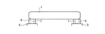
ここで、図面を参照しながらステッパーにおける基板の吸着機構を示す。
図7は、ステッパーの基板保持装置に吸着された基板の模式的な側面図である。
図7において、基板1は基板保持装置5に基板保持部材6により吸着されてセットされる。基板保持部材6は、基板1の2辺に沿った周辺の領域に設けられており、吸引口7を介して真空装置(図示せず)に接続されており、この吸引口7により吸引されて基板1がセットされる。
その際に、基板1の周縁部の端部形状が悪いと、真空チャックの際に基板1が変形し、それに伴いレチクルも変形してしまう。この結果、転写パターンのパターン位置精度、即ち転写パターン間の距離のずれや、線幅の均一性が悪化してしまうという問題点があった。
【0006】
そこで、基板の周縁部の端部形状を、数十nm(20〜30nm程度)以下に制御するという必要性から、特許文献1に記載されている加工方法が提案されている。
【0007】
【特許文献1】
特開2002−318450号公報
【0008】
特許文献1の加工方法は、露光機内においてフォトマスクが保持される部分に該当するガラス基板の部分を平坦にするため、ガラス基板形状と原料ガラス基板との形状の差分を計算し、この計算結果に応じて、原料ガラス基板に対し局所的なプラズマエッチングを施すというものである。
【0009】
【発明が解決しようとする課題】
しかし、上述の加工方法は以下のような問題点がある。
▲1▼局所的にプラズマエッチングされたガラス基板は、面荒れが生じたり、加工変質層が生じる。そのため、プラズマエッチングの後に、面荒れに起因する粗さの低減、及び加工変質層を除去するための研磨工程が必要となり、平坦度を悪化させてしまうことがある。
▲2▼プラズマエッチングによる加工では、プラズマエッチング前の基板の表面形状を精度良く測定することが必要となるが、この測定に用いられる光学干渉式の平坦度測定機等、一般の測定装置は、基板の周縁部では測定精度が悪いために、精度の良い測定をおこなうことが困難である。この結果、基板を所望の形状に作りこむことが難しい。
▲3▼基板の形状測定、プラズマエッチング、プラズマエッチング後の研磨、を行うための装置、工程が必要となる。
【0010】
そこで、本発明は上述の問題点に鑑みてなされたものであり、第一に、簡便な方法により、所望の平坦度で、且つ基板の周縁部の端部形状を数十nm(20〜30nm程度)以下に制御することが可能なマスクブランクス用基板の製造方法、及びマスクブランクスの製造方法を提供することを目的とする。
第二に、露光装置に装着しても、転写マスクの変形を抑制し、転写パターンの位置精度の低下を最小限に抑えられる転写マスクの製造方法を提供することを目的とする。
【0011】
【課題を解決するための手段】
従来のマスクブランクス用基板の製造方法は、所望の大きさ、形状に切断、面取加工を施されたマスクブランクス用基板を準備し、この準備されたマスクブランクス用基板に対し、基板表面の研削加工、基板端面の端面研磨加工、基板表面を鏡面に仕上げる研磨加工の順序で加工を行っていた。そして、研削加工、研磨加工は、使用される研削装置、研磨装置において、マスクブランクス用基板をキャリアなどの基板保持手段によって保持し、この保持された基板を研磨パッドが貼りつけられた上下定盤に挟持させ、基板表面の両面を同時に研削加工、研磨加工するものであった。この両面加工方法においては、基板の中心部であれば、表面形状を比較的制御し易いが、基板の周縁部にあっては、表面形状は制御しずらい。これは、マスクブランクス用基板に求められる、微細欠陥をなくすという目的から、比較的軟質な研磨パッドを使用して研磨するので、基板の周縁部は、研磨パッドからの過剰な圧力が加わったり、研磨パッドの当たり方が不安定になるからであると考えられる。
【0012】
上記課題を解決するために、本発明は以下の構成を要する。
第1の構成は、マスクブランクス用基板の製造方法であって、
前記マスクブランクス用基板の大きさよりも大きい基板材料を準備する基板材料準備工程と、
前記基板材料の主表面を研削、研磨し、少なくとも前記マスクブランクス用基板の大きさに相当する領域を、所望の表面粗さと所望の表面形状とに仕上げる研削・研磨工程と、
前記研削・研磨工程を経て得られた前記基板材料を、前記マスクブランクス用基板の大きさに切断する切断工程と、を有することを特徴とするマスクブランクス用基板の製造方法である。
【0013】
上述の構成によれば、表面形状が良好で、且つ制御が比較的容易な基板材料の略中心部分を、研削・研磨工程を終えた基板材料から切り出して、マスクブランクス用基板を得るので、所望の平坦度で、且つ基板の周縁部の端部形状が良好なマスクブランクス用基板を得ることができる。
尚、本発明でいう表面形状とは、平坦度やある特定領域でのうねりや基板周縁部の端部形状などを指す広い概念をいう。
【0014】
第2の構成は、前記切断工程により得られたマスクブランクス用基板へ、さらに面取りを行う形状加工工程を有することを特徴とする第1の構成記載のマスクブランクス用基板の製造方法である。
【0015】
上述の構成によれば、基板の面取りを行う形状加工を、研削・研磨工程の後(且つ、切断工程の後)に行うので、基板周縁部の端部形状を悪化させることがない。
【0016】
第3の構成は、前記研削・研磨工程の後、前記基板材料の主表面の表面形状を測定し、所望の表面粗さと所望の表面形状とを有する切断領域を決定する切断領域決定工程を有する、ことを特徴とする第1又は第2の構成記載のマスクブランクス用基板の製造方法である。
【0017】
上述の構成によれば、研削・研磨工程の後に基板材料の表面の表面形状を測定し、所望の表面粗さと所望の表面形状とを有する切断領域を決定し、この部分を切断領域とすることで、より確実に且つ最適な基板の形状精度を有するマスクブランクス用基板を得ることができる。
【0018】
第4の構成は、第1乃至第3構成記載のマスクブランクス用基板の製造方法によって得られたマスクブランクス用基板上に、被転写体に転写すべく転写パターンとなる薄膜を形成することを特徴とするマスクブランクスの製造方法である。
【0019】
上述の構成によれば、第1乃至第3構成記載のマスクブランクス用基板の製造方法によって得られたマスクブランクス用基板を使用してこの基板上に、被転写体に転写すべく転写パターンとなる薄膜を形成することで、ステッパーに装着しても、転写パターンのパターン位置精度、即ち転写パターン間の距離のずれや、線幅の均一性が良好な転写マスクとなる、当該転写マスクの原版であるマスクブランクスが得られる。
【0020】
第5の構成は、第4の構成記載のマスクブランクスの製造方法によって得られたマスクブランクスの前記薄膜をパターニングして、転写パターンを形成する転写マスクの製造方法である。
【0021】
上述の構成によれば、ステッパーに装着しても、転写パターンのパターン位置精度、即ち転写パターン間の距離のずれや、線幅の均一性が良好な転写マスクが得られる。
【0022】
【発明の実施の形態】
(基板材料)
準備する基板材料の大きさは、最終的に切断工程で切断するマスクブランクス用基板の大きさによって適宜選定する。例えば、マスクブランクス用基板が6025サイズ(大きさが152.4mm×152.4mm)の場合、準備する基板材料の大きさは9025サイズ(228.6mm×228.6mm)や8025サイズ(203.2mm×203.2mm)などを使用することができる。
【0023】
マスクブランクス用基板の大きさに比べて準備する基板材料の大きさが大きすぎると、切断した後、無駄になる基板材料が多くなるので、結果的に製造コストが上がるので好ましくない。また、マスクブランクス用基板の大きさに比べて準備する基板材料の大きさが、ほぼ同等のサイズであると、基板形状の良好な領域を切断して選択できる幅が小さくなり、更には、研磨パッドからの過剰な圧力や、研磨パッドの当たり方の不安定の領域にかかり、基板の周縁部の形状精度が悪い領域を使用しなければならなくなるので好ましくない。好ましくは、準備する基板材料の面積は、切断して得られるマスクブランクス用基板の主表面が有する面積の1.5〜3倍の範囲とすることが望ましい。この構成を採ることにより、研磨パッドからの過剰な圧力が加わったり、研磨パッドの当たり方が不安定となる基板の周縁部の領域を使用することを回避することができる。
【0024】
また、表面粗さ、表面形状は、転写マスクが使用される露光装置の露光光源に応じて決定すればよい。
【0025】
また、基板の材料は、後述するマスクブランクスの種類(透過型マスクブランクス、反射型マスクブランクス)と、露光光源の露光波長とに応じて選定する。材料としては一般にガラスが挙げられ、合成石英ガラス、ソーダライムガラス、低膨張ガラスなどが挙げられる。
【0026】
(切断方法)
切断工程における基板の切断方法は、特に限定されない。ダイヤモンドカッターなどの切断工具を用いて機械的に切断する方法、レーザー光などの光学的又は熱的エネルギーを利用して切断する方法などがある。基板の材料に応じて、切断した後の基板周縁部の端部形状に影響を与えない切断方法を選定する。
ダイヤモンドカッターなどの切断工具を用いて機械的に切断する場合、切断面からの亀裂等の欠陥を防止するために、基板上に保護膜を形成してから切断を行うと良い。保護膜の材料としては、基板が侵食されて表面粗さや平坦度などに影響を与えない薬液で除去できる材料が良い。
【0027】
(形状加工)
形状加工工程は、基板の面取り加工、基板の四隅(角)をR(丸)形状に加工するR(丸)仕上げ加工、基板の種類を見分けるノッチマークを形成するノッチマーク形成加工などを含む。形状加工工程の後、基板からの発塵を防止する意味で、基板の端面を鏡面に研磨する端面研磨を行っても良い。尚、基板の端面とは、基板側面、基板主表面と基板側面との間に形成している面取面を含む。
【0028】
端面研磨の方法には特に制限はない。例えば、研磨ブラシを用いるブラシ研磨方法、基板の端面形状と同じ形状を有する知具に研磨パッドを貼りつけたものを押付けて研磨するパッド研磨方法、テープを巻きつけた回転ローラーを押付けて研磨するテープ研磨方法、ベルト状の研磨体を押付けて研磨するベルト式研磨方法などが挙げられる。好ましくは、基板の周縁部の端部形状を悪化させない研磨パッドを用いる方法、テープ研磨方法、ベルト式面磨方法などが良い。
【0029】
(マスクブランクス)
本発明でいうマスクブランクスは、透過型マスクブランクス、反射型マスクブランクスの何れも指し、これらの構造は、基板上に被転写体に転写すべく転写パターンとなる薄膜を有する。尚、薄膜上にレジスト膜を形成したものでもよい。
【0030】
透過型マスクブランクスは、基板として透光性基板を使用し、転写パターンとなる薄膜は、被転写体に転写するときに使用する露光光に対し光学的変化をもたらす薄膜(例えば、遮光機能を有する薄膜)が使用されたフォトマスクブランクスである。ここで、露光光に対し光学的変化をもたらす薄膜とは、露光光を遮断する遮光膜や、露光光の位相差を変化させる位相シフト膜などを指す。また、遮光機能を有する薄膜とは、遮光機能と位相シフト機能を有する所謂ハーフトーン膜と、遮光機能を有する遮光膜とを含む。
従って、透過型マスクブランクスは、遮光膜が形成されたフォトマスクブランクス、ハーフトーン膜が形成された位相シフトマスクブランクス(ハーフトーン型位相シフトマスクブランクス)、位相シフト膜が形成された位相シフトマスクブランクスなどを含む。
【0031】
また、反射型マスクブランクスは、基板として熱膨張係数の小さいものを使用し、この基板上に光反射多層膜、転写パターンとなる光吸収体膜とを有するマスクブランクスである。
また、本発明のマスクブランクスには、上述の膜以外に、レジスト下地反射防止膜(BARC:Bottom Anti−Reflective Coating)、レジスト上層反射防止膜(TARL:Top Anti−Reflective Layer)、レジスト上層保護膜、導電性膜等の膜が形成されても良い。
【0032】
以上、説明したように、本発明のマスクブランクス用基板の製造方法、及びマスクブランクスの製造方法によれば、局所プラズマエッチングのような大掛かりな装置を必要とせず、簡便な方法で、所望の平坦度で、且つ基板の周縁部の端部形状を数十nm(20〜30nm程度)以下に制御することが可能なマスクブランクス用基板の製造方法、及びマスクブランクスの製造方法を提供することができる。
【0033】
<実施例>
以下に、図面を参照しながら実施例を用いて、本発明のマスクブランクス用基板の製造方法について説明する。
図1は、本発明のマスクブランクス用基板の製造方法を説明する工程フロー図である。
図1に示すように、マスクブランクスの製造方法は、大きく分けて、マスクブランクス用基板の大きさよりも大きい基板材料を準備する基板材料準備工程(P100)、マスクブランクス用基板の大きさに相当する領域において所望の表面粗さと所望の表面形状(平坦度)に仕上げる研削・研磨工程(P110)、マスクブランクス用基板の大きさに切断する切断工程(P120)、基板の面取りを行う形状加工工程(P130)、基板の端面を研磨する端面研磨工程(P140)、基板上に薄膜を形成する前に基板を洗浄する成膜前洗浄工程(P150)とを有する。尚、研削・研磨工程(P110)と切断工程(P120)の間に、基板の表面形状を測定する形状測定工程(P111)と切断領域を決定する切断領域決定工程(P112)を設けても良い。また、各工程間に基板を洗浄する洗浄工程を設けても良い。
【0034】
以下、各工程を詳細に説明する。
(a)基板材料準備工程(P100)
マスクブランクス用基板として6025サイズ(基板主表面の大きさ:152.4mm×152.4mm)を得るため、基板材料として9025サイズ(基板主表面の大きさ:228.6mm×228.6mm)の合成石英ガラスからなる基板材料10を準備した。この基板材料は、合成石英ガラスブロックから、上述のサイズに切り出した状態のものである。
【0035】
(b)研削・研磨工程(P110)
この研削・研磨工程は、詳述すると、基板材料の反りの除去、及び平坦度、板厚の制御を目的とする研削工程(ラッピング工程)と、研削工程で得られた形状、平坦度を維持又は向上しつつ、欠陥を除去し所望の表面粗さに仕上げる研磨工程(ポリッシング工程)とに分かれる。
【0036】
研削工程における研削方法(ラッピング方法)としては、一般にキャリアと呼ばれる保持器具によって保持された基板材料を、上下定盤内に挟持し、上下定盤及びキャリアを回転させつつ、基板材料の両面に液体の砥粒を供給する両面研削方法(両面ラッピング方法)を行う。尚、上下定盤としては、碁盤の目状に溝が形成された鋳鉄状の定盤を使用する。砥粒は、粗研削用と精研削用とに分類され、粗研削としては炭化珪素、アルミナ等#400〜#600程度のものを用い、精研削では、アルミナ、ジルコニア等#800〜#1500程度の砥粒を使用する。
【0037】
研磨工程における研磨方法(ポリッシング方法)としては、上述のラッピング方法と同様に、一般にキャリアによって保持された基板材料を上下定盤内に挟持し、研磨パッドが貼りつけられた上下定盤及びキャリアを回転させつつ基板材料の両面に液体のポリッシング用スラリーを供給する両面研磨方法(両面ポリッシング方法)を行う。研磨工程は、通常、粗研磨工程、精密研磨工程、…というように複数段階に分けて行う。そして、研磨パッドは、粗研磨工程では、加工能率と平坦性を重視して、発泡ポリウレタンなどの硬質ポリシャを使用し、精密研磨工程では、欠陥の除去と表面粗さの低減を重視して、軟質スウェードタイプの軟質ポリシャを使用する。スラリーとしては、粗研磨工程、精密研磨工程と進行するに従って、次第に平均粒径が小さいものを使用する。スラリーとしては、酸化セリウム、ジルコニア、コロイダルシリカ等が挙げられる。
【0038】
本実施例では、以下のような研削・研磨条件で研削・研磨工程を行った。
粗研削工程
上述の両面研削方法を採用。使用砥粒は#400アルミナ砥粒。
精研削工程
上述の両面研削方法を採用。使用砥粒は#800アルミナ砥粒。
粗研磨工程
上述の両面研磨方法を採用。発泡ポリウレタンの研磨パッド、平均粒径1〜2μmの酸化セリウム砥粒を使用。
精密研磨工程
上述の両面研磨装置を採用。軟質スウェードタイプの研磨パッド、平均粒径80〜100nmのコロイダルシリカ砥粒を使用。
尚、各研削・研磨工程間で、低濃度のフッ酸水溶液による洗浄を行った。
【0039】
上述の研削・研磨工程を経て得られた基板材料において、中心領域6025サイズ(152.4mm×152.4mm)の表面粗さ、及び平坦度を測定したところ、表面粗さRMS(二乗平均(平方根)粗さ)は0.13nm、平坦度は0.25μmであった。尚、表面粗さは、AFM(原子間力顕微鏡)(デジタルインスツルメンツ社製ナノスコープ)で測定し、平坦度は、光学干渉式の平坦度測定機(トロッペル社製FM300)で測定した。
【0040】
(c)切断工程(P120)
上述の基板材料に6025サイズの切断領域にマーキングを施した後、透明な保護膜を厚さ約3μm、基板材料の全面に浸漬法により形成した。その後、マーキングに沿ってダイヤモンドカッターで切断し、基板材料から6025サイズのガラス基板を得た。
【0041】
(d)形状加工工程(P130)
ガラス基板の略主表面全面に保護膜が形成された状態で、以下のように基板の面取り加工、R(丸)仕上げ加工、ノッチマーク形成加工を行った。
この面取り加工、R(丸)仕上げ加工、ノッチマーク形成加工について、図2〜図4を参照しながら説明する。
ここで、図2は、面取加工装置を用いた面取り加工の概念的な斜視図であり、図3は、基板の面取り加工や、R(丸)仕上げ加工を行う面取加工装置の概念的な側面図であり、図4は 基板のノッチマーク加工を行うノッチマーク形状加工装置の概念的な側面図である。
【0042】
図2〜4において、符号10は切断工程で得られたガラス基板であり、符号20はガラス基板10に形成された保護膜であり、符号30は面取り用砥石であり、符号40はスピンドルモータである。また図3において、符号31は面取り用砥石30の凹溝である。さらに図4において、符号50はノッチマーク加工用砥石であり、符号60はスピンドルモータである。
【0043】
まず、図2、3を用いてガラス基板の面取り加工について説明する。
図2、3に示すように、基板側面に凹溝を有する円柱状の面取り用砥石30がスピンドルモータ40の回転軸の先端に装着され、このスピンドルモータ40は、NC加工装置(図示せず)の加工ヘッドに取り付けられている。この面取加工装置を用いて、ガラス基板10の側面に面取り用砥石30の凹溝31を押し当て、スピンドルモータ40を回転させつつ、ガラス基板10の周囲を一周させることによって面取り加工を行った。
【0044】
R(丸)仕上げ加工も、図3に示した面取加工装置を使用し、ガラス基板10の側面が交差する四隅の角部に対し、面取り用砥石30の凹溝31を押し当て、R(丸)仕上げ加工を行った。
【0045】
ノッチマーク形成加工は、図4に示したノッチマーク形成加工装置を使用して行った。ノッチマーク形成加工装置は、円錐状のノッチマーク加工用砥石50を装着したスピンドルモータ60を、NC加工装置(図示せず)の加工ヘッドに取りつけたものである。このノッチマーク形成加工装置を用いて、ガラス基板10の対向する角部にノッチマーク用砥石50を押し当てて、ノッチマークの形状加工を行った。
【0046】
(e)端面研磨工程(P140)
形状加工工程を終えたガラス基板の端面(側面及び面取面)の研磨を、端面研磨装置を使用して行った。この端面の研磨について、図5、6を参照しながら説明する。
ここで、図5は、当該端面研磨に用いる端面研磨装置の模式的な側面図であり、図6は、図5をA矢視したときの部分拡大図である。
まず、図5において、符号10はガラス基板であり、符号70は基板保持具であり、符号80は研磨治具であり、符号90は研磨砥粒を含むスラリーであり、符号100は研磨液供給ノズルである。図6において、符号10はガラス基板であり、符号80は研磨治具であり、符号81は基板の端面と同じ形状の溝であり、符号82は研磨パッドである。
【0047】
図5に示すように、この端面研磨装置は、複数のガラス基板10を基板保持具70の上方へ平行に配列した状態でセットし、このガラス基板10の側面に研磨治具80が配置され、研磨砥粒を含むスラリー90が研磨液供給ノズル100よりガラス基板10の側面に向けて供給されるものである。
ここで、図6に示すように、このガラス基板10の側面は、当該基板の側面と同じ形状を有する溝81の表面に、研磨パッド82を貼りつけた研磨治具80と接触している。
【0048】
ここで、図5に戻りガラス基板10の端面研磨操作について説明する。
まず、研磨砥粒を含むスラリー90を研磨液供給ノズル100よりガラス基板10の側面に向けて供給し、この研磨治具80をガラス基板10の側面に沿って往復運動させて端面研磨を行う。尚、スラリーに用いた研磨砥粒は、上述の精密研磨工程で使用した粒径と同じか又は小さい平均粒径のコロイダルシリカを用いた。
【0049】
(f)成膜前洗浄工程(P150)
ガラス基板の端面に付着した研磨砥粒と、ガラス基板主表面の略全面に形成されている保護層をアルカリ水溶液で洗浄して、F2エキシマレーザー露光用のマスクブランクス用基板を得た。得られたガラス基板の表面粗さ、及び平坦度を測定したところ、上述の測定結果と殆ど変化はなかった。
また、端部形状の最大高さは、―0.02μmであった。尚、端部形状は、基板主表面と面取面との境界から基板の中心方向に3〜16mmを仮想基準面(0)としたときに、主表面と面取面との境界から3mmの位置における最大高さで評価した。最大高さが負の場合は、基板の周縁部が垂れている形状(所謂、縁ダレ形状)を示し、最大高さが正の場合は、基板の周縁部が盛りあがった形状を示す。尚、端部形状は、触針式形状測定器(ミツトヨ社製:サーフテスト−501)で測定した。
【0050】
以下、マスクブランクスの製造方法、及び転写マスクの製造方法について説明する。
上述のマスクブランクス用基板の製造方法によって得られたガラス基板上に、スパッタリング法によりクロム膜と酸化クロム膜からなる合計膜厚が1000Åの反射防止膜付き遮光膜を形成した。次ぎに、当該遮光膜上にスピンコート法によりレジスト膜を形成し、さらにプリベーク処理を行い、レジスト膜付きマスクブランクスを得た。
得られたマスクブランクスのレジスト膜に対し、被転写体に転写すべくパターンを露光、現像処理を行いレジストパターンを形成した。次ぎに、レジストパターンをマスクにして遮光膜をウェットエッチングで除去して、レジスト膜を除去して、遮光膜からなる転写パターンをガラス基板上に形成した転写マスクを得た。
【0051】
ここで、得られた転写マスクの基板変形試験を行うために、図7を用いて説明した露光装置(ステッパー)の基板保持部材と同様に、基板の2辺を真空チャックする基板変形試験機を準備した。そして、この基板変形試験機へ、上述の実施例によって得られた転写マスク(レチクル)を真空チャックによりチャッキングし、光学式干渉計(ZygoMarkGPI)で平坦度変化量を測定したところ、0.1μm以下となり、基板変形はほとんど認められなかった。
【0052】
<比較例>
合成石英ガラスブロックから、6025サイズに切り出したマスクブランクス用基板の基板材料を準備し、実施例に記載した形状加工工程、研削工程、端面研磨工程、研磨工程をこの順で、実施例と同じ加工方法で加工を行い、マスクブランクス用基板を得た。次ぎに、得られた基板の表面形状(平坦度)を光学干渉式の平坦度測定機により測定し、基板周縁部を除く領域及び転写マスク保持部位に相当する領域の測定データをもとに、基板周縁部を除く領域が平坦度0.25μm以下、転写マスク保持部位に相当する領域の平坦度が20〜30nm以下となるための必要除去量を決定し、基板表面の局所プラズマエッチングを行った。尚、エッチングガスとしては、四弗化メタンを使用した。その後、局所プラズマエッチングによる荒れを平滑化するために、極く短時間の研磨処理を行い、マスクブランクス用基板を得た。
【0053】
得られたマスクブランクス用基板の基板周縁部を除く領域の平坦度は、0.25μm以下と良好であったが、端部形状は、−1.5μmとなった。これは、基板周縁部領域の形状測定の測定精度が悪いことと、局所プラズマエッチング後の研磨処理により端部形状が制御しきれずに悪化したためと考えられる。
【0054】
また、上述の実施例と同様にマスクブランクス及び転写マスクを作製した。 上述と同様の基板変形試験を行こなったところ、転写マスク(レチクル)を真空チャックによりチャッキングし、光学式干渉計(ZygoMarkGPI)での平坦度変化量が0.5μmを超える結果となった。
【0055】
上述の、実施例及び比較例の結果より、実施例に示す本発明の製造方法を採用することにより、露光装置(ステッパー)に装着しても、転写マスクの変形を抑制することができるので、転写パターンの位置精度の低下を最小限に抑えることができる。
【0056】
尚、上述の実施例では、マスクブランクス用基板の大きさよりも大きい基板材料の研削・研磨工程を終えた基板材料から、マスクブランクス用基板の大きさに切断する際、予め決定しておいた中心領域を選択して切断したが、基板の表面形状を測定した後、測定結果に従って所望の表面粗さと所望の表面形状である切断領域を決定してから、切断しても良い。
【0057】
【発明の効果】
本発明は、マスクブランクス用基板の製造方法であって、
前記マスクブランクス用基板よりも大きな表面積を有する基板材料を準備する基板材料準備工程と、
前記基板材料の主表面を研削、研磨し、少なくとも前記マスクブランクス用基板の大きさに相当する領域を、所望の表面粗さと所望の表面形状とに仕上げる研削・研磨工程と、
前記研削・研磨工程を経て得られた前記基板材料を、前記マスクブランクス用基板の大きさに切断する切断工程と、を有するものであり、当該製造方法を用いることにより、簡便な方法で、所望の平坦度で、且つ基板の周縁部の端部形状が良好なマスクブランクス用基板を得ることができる。
【図面の簡単な説明】
【図1】本発明のマスクブランクス用基板の製造方法を説明する図である。
【図2】基板の面取り加工や、R(丸)仕上げ加工を行う面取加工装置を示す図である。
【図3】基板の面取り加工や、R(丸)仕上げ加工を行う面取加工装置を示す図である。
【図4】基板のノッチマーク加工を行うノッチマーク形状加工装置を示す図である。
【図5】基板の端面(側面及び面取面)を研磨する端面研磨装置を示す図である。
【図6】図5をA矢視したときの部分拡大図である。
【図7】ステッパーにおける基板吸着機構を示す図である。
【符号の説明】
1 基板
5 基板保持装置
6 基板保持部材
7 吸引口
10 基板材料(ガラス基板)
11 遮光膜
12 レジスト膜
20 保護膜
30 面取り用砥石
31 凹溝
40 スピンドルモータ
60 スピンドルモータ
50 ノッチマーク加工用砥石
70 基板保持具
80 研磨治具
81 溝
82 研磨パッド
90 スラリー
100 研磨液供給ノズル[0001]
TECHNICAL FIELD OF THE INVENTION
The present invention is mounted on an exposure apparatus (hereinafter, sometimes referred to as a stepper) used for manufacturing a semiconductor integrated circuit and the like, and is provided with a transfer mask for a reduced exposure apparatus (hereinafter, sometimes referred to as a reticle). The present invention relates to a mask blank substrate used as a mask, a mask blank using the substrate, and a method for manufacturing a transfer mask.
[0002]
[Prior art]
For example, in the manufacture of a semiconductor integrated circuit, a reticle mounted on a stepper for pattern transfer and used as a transfer mask for a reduction exposure apparatus is formed by a sputtering method on a glass substrate whose main surface is mirror-finished. In this case, a pattern made of a light-shielding film containing chromium or the like is formed.
[0003]
This glass substrate is required to have a high flatness on the main surface of the substrate in order to form a pattern having a high pattern position accuracy on a transferred body in a pattern transfer region, for example, in the manufacture of a semiconductor integrated circuit. ing. In recent years, for example, with respect to a substrate of 6025 size (152.4 mm × 152.4 mm × 6.35 mm), the flatness in a region excluding 3 mm from the side surface of the substrate is 0.5 μm or less (ArF excimer laser exposure substrate). , 0.25 μm or less (substrate for F2 excimer laser exposure) and 0.05 μm or less (substrate for EUV exposure). The flatness is defined by the difference between the maximum value and the minimum value of the measurement plane with respect to a virtual absolute plane (focal plane) calculated from the measurement plane by the least square method. Conventionally, as described above, flatness of a region excluding the peripheral region on the main surface of the substrate has been required.
[0004]
However, with the recent miniaturization of patterns of semiconductor integrated circuits and the like, as the pattern line width becomes smaller, the pattern position accuracy when transferring a pattern on a reticle to a transfer target using a stepper is more than that of a glass substrate. It was found that the shape of the peripheral region had an effect.
Usually, in a stepper, the reticle is mounted with the main surface of the substrate on which the pattern is formed facing the object to be transferred. At this time, the reticle is vacuum-chucked using the peripheral portion of the main surface of the substrate so that the pattern area of the reticle is widened and the reticle does not shift during operation of the stepper.
[0005]
Here, the substrate suction mechanism of the stepper will be described with reference to the drawings.
FIG. 7 is a schematic side view of the substrate sucked by the substrate holding device of the stepper.
In FIG. 7, the substrate 1 is set on the
At this time, if the shape of the edge of the peripheral portion of the substrate 1 is bad, the substrate 1 is deformed at the time of vacuum chuck, and the reticle is deformed accordingly. As a result, there has been a problem that the pattern position accuracy of the transfer pattern, that is, the deviation of the distance between the transfer patterns and the uniformity of the line width are deteriorated.
[0006]
Therefore, a processing method described in Patent Literature 1 has been proposed from the necessity of controlling the end shape of the peripheral portion of the substrate to several tens nm (about 20 to 30 nm) or less.
[0007]
[Patent Document 1]
JP 2002-318450 A
[0008]
The processing method of Patent Document 1 calculates a difference between the shape of the glass substrate and the shape of the raw glass substrate in order to flatten a portion of the glass substrate corresponding to a portion where the photomask is held in the exposure machine, and calculates the calculation result. In accordance with the above, local plasma etching is performed on the raw glass substrate.
[0009]
[Problems to be solved by the invention]
However, the above-mentioned processing method has the following problems.
{Circle around (1)} A glass substrate that has been locally plasma-etched has a roughened surface or a damaged layer. For this reason, after the plasma etching, a polishing step for reducing roughness due to surface roughness and removing a damaged layer is required, which may deteriorate the flatness.
{Circle around (2)} In processing by plasma etching, it is necessary to accurately measure the surface shape of the substrate before plasma etching. However, general measuring devices such as an optical interference type flatness measuring device used for this measurement include: Since the measurement accuracy is low at the periphery of the substrate, it is difficult to perform accurate measurement. As a result, it is difficult to form the substrate into a desired shape.
(3) An apparatus and a process for measuring the shape of the substrate, plasma etching, and polishing after the plasma etching are required.
[0010]
Therefore, the present invention has been made in view of the above-described problems, and firstly, by a simple method, the end shape of the peripheral portion of the substrate with desired flatness is several tens nm (20 to 30 nm). Degree) It is an object of the present invention to provide a method for manufacturing a mask blank substrate and a method for manufacturing a mask blank, which can be controlled as follows.
Secondly, it is an object of the present invention to provide a method of manufacturing a transfer mask capable of suppressing deformation of a transfer mask even when the transfer mask is mounted on the exposure apparatus and minimizing a decrease in positional accuracy of a transfer pattern.
[0011]
[Means for Solving the Problems]
The conventional method of manufacturing a mask blank substrate is to prepare a mask blank substrate cut and chamfered to a desired size and shape, and grind the substrate surface to the prepared mask blank substrate. Processing was performed in the order of processing, polishing of the end face of the substrate, and polishing to finish the substrate surface to a mirror surface. Then, in the grinding and polishing processes, the substrate for mask blanks is held by a substrate holding means such as a carrier in a used grinding device or polishing device, and the held substrate is an upper and lower platen to which a polishing pad is attached. , And both sides of the substrate surface are simultaneously ground and polished. In this double-sided processing method, the surface shape is relatively easy to control in the central portion of the substrate, but it is difficult to control the surface shape in the peripheral portion of the substrate. This is required for the mask blank substrate, for the purpose of eliminating fine defects, polishing using a relatively soft polishing pad, the peripheral portion of the substrate, or excessive pressure from the polishing pad, It is considered that the contact with the polishing pad becomes unstable.
[0012]
In order to solve the above problems, the present invention requires the following configurations.
The first configuration is a method of manufacturing a substrate for mask blanks,
A substrate material preparation step of preparing a substrate material larger than the size of the mask blanks substrate,
Grinding and polishing the main surface of the substrate material, at least a region corresponding to the size of the mask blanks substrate, a grinding and polishing step to finish a desired surface roughness and a desired surface shape,
A cutting step of cutting the substrate material obtained through the grinding / polishing step into a size of the mask blank substrate.
[0013]
According to the above-described configuration, a substantially central portion of the substrate material having a good surface shape and relatively easy to control is cut out from the substrate material after the grinding / polishing step to obtain a mask blank substrate. It is possible to obtain a mask blank substrate having a good flatness and a good edge shape at the periphery of the substrate.
In addition, the surface shape in the present invention has a broad concept indicating flatness, undulation in a specific region, end shape of a peripheral portion of a substrate, and the like.
[0014]
A second configuration is the method for manufacturing a mask blank substrate according to the first configuration, further comprising a shape processing step of chamfering the mask blank substrate obtained in the cutting step.
[0015]
According to the above configuration, the shape processing for chamfering the substrate is performed after the grinding / polishing step (and after the cutting step), so that the end shape of the peripheral portion of the substrate is not deteriorated.
[0016]
The third configuration has a cutting area determining step of measuring a surface shape of a main surface of the substrate material after the grinding / polishing step, and determining a cutting area having a desired surface roughness and a desired surface shape. A method of manufacturing a substrate for mask blanks according to the first or second configuration, characterized in that:
[0017]
According to the above configuration, after the grinding / polishing step, the surface shape of the surface of the substrate material is measured, a cutting region having a desired surface roughness and a desired surface shape is determined, and this portion is set as a cutting region. Thus, it is possible to more reliably obtain a mask blank substrate having the optimum substrate shape accuracy.
[0018]
A fourth configuration is characterized in that a thin film serving as a transfer pattern is formed on a mask blank substrate obtained by the method for manufacturing a mask blank substrate according to any one of the first to third configurations so as to be transferred to a transfer target. Is a method of manufacturing a mask blank.
[0019]
According to the above configuration, a transfer pattern is formed on the substrate using the mask blank substrate obtained by the method for manufacturing a mask blank substrate according to any of the first to third configurations so that the transfer pattern is transferred onto the substrate. By forming a thin film, even when mounted on a stepper, the pattern position accuracy of the transfer pattern, i.e., the deviation of the distance between the transfer patterns and the uniformity of the line width become a good transfer mask. A certain mask blank is obtained.
[0020]
A fifth configuration is a method of manufacturing a transfer mask for forming a transfer pattern by patterning the thin film of the mask blank obtained by the method of manufacturing a mask blank according to the fourth configuration.
[0021]
According to the above configuration, even when the transfer mask is mounted on the stepper, a transfer mask having good pattern position accuracy of the transfer pattern, that is, a shift in the distance between the transfer patterns and a uniform line width can be obtained.
[0022]
BEST MODE FOR CARRYING OUT THE INVENTION
(Substrate material)
The size of the prepared substrate material is appropriately selected according to the size of the mask blank substrate to be finally cut in the cutting step. For example, when the mask blank substrate is 6025 size (152.4 mm × 152.4 mm), the size of the prepared substrate material is 9025 size (228.6 mm × 228.6 mm) or 8025 size (203.2 mm). × 203.2 mm) can be used.
[0023]
If the size of the prepared substrate material is too large compared to the size of the mask blank substrate, the amount of wasted substrate material after cutting is increased, which is not preferable because the production cost increases as a result. In addition, if the size of the substrate material to be prepared is substantially the same as the size of the substrate for the mask blank, the width that can be selected by cutting a region having a good substrate shape becomes small, and furthermore, polishing is performed. It is not preferable because an excessive pressure from the pad or an unstable area where the polishing pad comes into contact is applied, and an area where the shape accuracy of the peripheral portion of the substrate is poor must be used. Preferably, the area of the prepared substrate material is 1.5 to 3 times the area of the main surface of the mask blank substrate obtained by cutting. By adopting this configuration, it is possible to avoid using excessive pressure from the polishing pad or using the peripheral region of the substrate where the contact of the polishing pad becomes unstable.
[0024]
Further, the surface roughness and the surface shape may be determined according to the exposure light source of the exposure device using the transfer mask.
[0025]
The material of the substrate is selected in accordance with the type of mask blanks (transmission mask blanks and reflection mask blanks) described later and the exposure wavelength of the exposure light source. The material is generally glass, and examples include synthetic quartz glass, soda lime glass, and low expansion glass.
[0026]
(Cutting method)
The method for cutting the substrate in the cutting step is not particularly limited. There are a method of cutting mechanically using a cutting tool such as a diamond cutter, and a method of cutting using optical or thermal energy such as laser light. According to the material of the substrate, a cutting method that does not affect the end shape of the peripheral portion of the substrate after cutting is selected.
When cutting mechanically using a cutting tool such as a diamond cutter, it is preferable to cut after forming a protective film on a substrate in order to prevent defects such as cracks from the cut surface. As a material for the protective film, a material that can be removed with a chemical solution that does not affect the surface roughness or flatness due to erosion of the substrate is preferable.
[0027]
(Shape processing)
The shape processing step includes chamfering of the substrate, R (round) finishing for processing the four corners (corners) of the substrate into an R (circle) shape, and notch mark forming for forming a notch mark for identifying the type of the substrate. After the shape processing step, an end surface polishing for polishing the end surface of the substrate to a mirror surface may be performed in order to prevent dust generation from the substrate. The end surface of the substrate includes a side surface of the substrate and a chamfered surface formed between the main surface of the substrate and the side surface of the substrate.
[0028]
There is no particular limitation on the method of edge polishing. For example, a brush polishing method using a polishing brush, a pad polishing method of pressing and polishing a polishing tool having a polishing pad adhered to a tool having the same shape as the end face of the substrate, and pressing and polishing a rotating roller wound with a tape. A tape polishing method, a belt-type polishing method in which a belt-shaped polishing body is pressed and polished are exemplified. Preferably, a method using a polishing pad that does not deteriorate the end shape of the peripheral portion of the substrate, a tape polishing method, a belt-type surface polishing method, and the like are preferable.
[0029]
(Mask blanks)
The mask blanks referred to in the present invention refer to both transmission mask blanks and reflection mask blanks, and these structures have a thin film that becomes a transfer pattern to be transferred onto a substrate on a substrate. Incidentally, a resist film may be formed on a thin film.
[0030]
A transmissive mask blank uses a translucent substrate as a substrate, and a thin film serving as a transfer pattern is a thin film (for example, having a light-shielding function) that causes an optical change to exposure light used when transferring to a transfer target. This is a photomask blank in which a thin film is used. Here, the thin film that causes an optical change to the exposure light refers to a light-shielding film that blocks the exposure light, a phase shift film that changes the phase difference of the exposure light, and the like. Further, the thin film having a light shielding function includes a so-called halftone film having a light shielding function and a phase shift function, and a light shielding film having a light shielding function.
Accordingly, the transmission mask blanks include a photomask blank on which a light shielding film is formed, a phase shift mask blank on which a halftone film is formed (halftone phase shift mask blank), and a phase shift mask blank on which a phase shift film is formed. Including.
[0031]
The reflective mask blank is a mask blank using a substrate having a small coefficient of thermal expansion as a substrate, and having a light reflective multilayer film and a light absorber film serving as a transfer pattern on the substrate.
In addition, in addition to the above-mentioned films, the mask blank of the present invention includes a resist base anti-reflection film (BARC: Bottom Anti-Reflective Coating), a resist upper layer anti-reflection film (TARL: Top Anti-Reflective Layer), a resist upper layer protection film. Alternatively, a film such as a conductive film may be formed.
[0032]
As described above, according to the method for manufacturing a mask blank substrate and the method for manufacturing a mask blank of the present invention, a large-scale apparatus such as local plasma etching is not required, and a desired flatness can be obtained by a simple method. It is possible to provide a method of manufacturing a mask blank substrate and a method of manufacturing a mask blank, which can control the edge shape of the peripheral portion of the substrate to several tens nm (about 20 to 30 nm) or less. .
[0033]
<Example>
Hereinafter, a method of manufacturing a substrate for a mask blank of the present invention will be described using embodiments with reference to the drawings.
FIG. 1 is a process flow chart illustrating a method for manufacturing a mask blank substrate according to the present invention.
As shown in FIG. 1, the method of manufacturing a mask blank is roughly divided into a substrate material preparing step (P100) of preparing a substrate material larger than the size of the mask blank substrate, and corresponds to the size of the mask blank substrate. A grinding / polishing step (P110) for finishing a desired surface roughness and a desired surface shape (flatness) in a region, a cutting step (P120) for cutting into a size of a mask blank substrate, and a shape processing step for chamfering a substrate ( P130), an end surface polishing step (P140) for polishing the end surface of the substrate, and a pre-film formation cleaning step (P150) for cleaning the substrate before forming a thin film on the substrate. Incidentally, between the grinding / polishing step (P110) and the cutting step (P120), a shape measuring step (P111) for measuring the surface shape of the substrate and a cutting area determining step (P112) for determining the cutting area may be provided. . Further, a cleaning step of cleaning the substrate may be provided between each step.
[0034]
Hereinafter, each step will be described in detail.
(A) Substrate material preparation step (P100)
In order to obtain 6025 size (substrate main surface size: 152.4 mm × 152.4 mm) as a mask blank substrate, 9025 size (substrate main surface size: 228.6 mm × 228.6 mm) is synthesized as a substrate material. A
[0035]
(B) Grinding / polishing process (P110)
In detail, the grinding and polishing step includes a grinding step (lapping step) for removing the warpage of the substrate material and controlling the flatness and the plate thickness, and maintaining the shape and flatness obtained in the grinding step. Alternatively, the process is divided into a polishing process (polishing process) for removing defects and finishing to a desired surface roughness while improving.
[0036]
As a grinding method (lapping method) in the grinding process, a substrate material held by a holding device generally called a carrier is sandwiched between upper and lower platens, and liquid is applied to both surfaces of the substrate material while rotating the upper and lower platens and the carrier. A double-sided grinding method (double-sided lapping method) for supplying abrasive grains is performed. In addition, as the upper and lower surface plates, a cast iron-type surface plate having grooves formed in a grid pattern is used. Abrasive grains are classified into those for coarse grinding and those for fine grinding. For rough grinding, silicon carbide, alumina and the like having a size of about # 400 to # 600 are used, and for fine grinding, alumina and zirconia such as about # 800 to # 1500 are used. Use abrasive grains.
[0037]
As a polishing method (polishing method) in the polishing step, similarly to the above-described lapping method, generally, a substrate material held by a carrier is sandwiched between upper and lower platens, and the upper and lower platens and a carrier to which a polishing pad is attached are bonded. A double-side polishing method (double-side polishing method) for supplying a liquid polishing slurry to both surfaces of the substrate material while rotating is performed. The polishing step is usually performed in a plurality of steps such as a rough polishing step, a precision polishing step, and so on. The polishing pad uses a hard polisher such as polyurethane foam in the rough polishing process with emphasis on processing efficiency and flatness.In the precision polishing process, it focuses on removing defects and reducing surface roughness. Use a soft suede type soft polisher. As the slurry, a slurry having an gradually smaller average particle size is used as the rough polishing process and the fine polishing process progress. Examples of the slurry include cerium oxide, zirconia, and colloidal silica.
[0038]
In this example, the grinding / polishing process was performed under the following grinding / polishing conditions.
Rough grinding process
Adopts the double-sided grinding method described above. The abrasive used is # 400 alumina abrasive.
Fine grinding process
Adopts the double-sided grinding method described above. The abrasive used is # 800 alumina abrasive.
Rough polishing process
Adopts the double-side polishing method described above. A polishing pad made of foamed polyurethane and cerium oxide abrasive grains having an average particle size of 1 to 2 μm are used.
Precision polishing process
Adopts the above-mentioned double-side polishing machine. Uses a soft suede type polishing pad and colloidal silica abrasive having an average particle size of 80 to 100 nm.
In addition, between each grinding | polishing / polishing process, washing | cleaning by the hydrofluoric acid aqueous solution of a low concentration was performed.
[0039]
When the surface roughness and flatness of the central region 6025 size (152.4 mm × 152.4 mm) were measured on the substrate material obtained through the above-described grinding / polishing process, the surface roughness RMS (root mean square (root mean square)) was measured. ) Roughness) was 0.13 nm, and flatness was 0.25 μm. The surface roughness was measured with an AFM (Atomic Force Microscope) (Nanoscope manufactured by Digital Instruments Co., Ltd.), and the flatness was measured by an optical interference type flatness measuring device (FM300 manufactured by Tropel).
[0040]
(C) Cutting process (P120)
After marking the cutting area of the 6025 size on the above-mentioned substrate material, a transparent protective film having a thickness of about 3 μm was formed on the entire surface of the substrate material by an immersion method. Then, it cut | disconnected by the diamond cutter along the marking, and obtained the 6025 size glass substrate from the substrate material.
[0041]
(D) Shape processing step (P130)
With the protective film formed on the substantially entire main surface of the glass substrate, the substrate was subjected to chamfering, R (round) finishing, and notch mark forming as follows.
The chamfering, R (round) finishing, and notch mark forming will be described with reference to FIGS.
Here, FIG. 2 is a conceptual perspective view of a chamfering process using a chamfering device, and FIG. 3 is a conceptual diagram of a chamfering device for performing a chamfering process on a substrate and an R (round) finishing process. FIG. 4 is a conceptual side view of a notch mark shape processing apparatus that performs notch mark processing on a substrate.
[0042]
2 to 4,
[0043]
First, chamfering of a glass substrate will be described with reference to FIGS.
As shown in FIGS. 2 and 3, a column-shaped
[0044]
The R (round) finishing is also performed by using the chamfering apparatus shown in FIG. 3 and pressing the
[0045]
The notch mark formation processing was performed using the notch mark formation processing apparatus shown in FIG. The notch mark forming and processing apparatus is such that a
[0046]
(E) Edge polishing step (P140)
Polishing of the end face (side face and chamfered face) of the glass substrate after the shape processing step was performed using an end face polishing apparatus. The polishing of the end face will be described with reference to FIGS.
Here, FIG. 5 is a schematic side view of an end face polishing apparatus used for the end face polishing, and FIG. 6 is a partially enlarged view when FIG.
First, in FIG. 5,
[0047]
As shown in FIG. 5, this end face polishing apparatus sets a plurality of
Here, as shown in FIG. 6, the side surface of the
[0048]
Here, returning to FIG. 5, the operation of polishing the end face of the
First, a
[0049]
(F) Pre-film formation cleaning step (P150)
The polishing abrasive grains adhered to the end surface of the glass substrate and the protective layer formed on substantially the entire surface of the main surface of the glass substrate were washed with an alkaline aqueous solution to obtain a mask blank substrate for F2 excimer laser exposure. When the surface roughness and flatness of the obtained glass substrate were measured, there was almost no change from the above measurement results.
Further, the maximum height of the end portion shape was -0.02 μm. The end shape is 3 mm from the boundary between the main surface and the chamfered surface when the virtual reference plane (0) is 3 to 16 mm in the center direction of the substrate from the boundary between the main surface and the chamfered surface. Evaluation was made based on the maximum height at the position. When the maximum height is negative, a shape in which the peripheral edge of the substrate hangs (a so-called edge sagging shape) is shown, and when the maximum height is positive, a shape in which the peripheral edge of the substrate rises. The end shape was measured with a stylus type shape measuring device (Mitutoyo Corporation: Surf Test-501).
[0050]
Hereinafter, a method for manufacturing a mask blank and a method for manufacturing a transfer mask will be described.
On a glass substrate obtained by the above-described method for manufacturing a mask blank substrate, a light-shielding film with an anti-reflection film having a total film thickness of 1000 ° and comprising a chrome film and a chromium oxide film was formed by sputtering. Next, a resist film was formed on the light-shielding film by a spin coating method, and prebaking was performed to obtain a mask blank with a resist film.
The resist film of the obtained mask blanks was exposed to a pattern and developed to transfer it to a transfer target, thereby forming a resist pattern. Next, the light-shielding film was removed by wet etching using the resist pattern as a mask, and the resist film was removed to obtain a transfer mask in which a transfer pattern composed of the light-shielding film was formed on a glass substrate.
[0051]
Here, in order to perform a substrate deformation test of the obtained transfer mask, a substrate deformation tester that vacuum chucks two sides of the substrate is used in the same manner as the substrate holding member of the exposure apparatus (stepper) described with reference to FIG. Got ready. Then, the transfer mask (reticle) obtained in the above embodiment was chucked by a vacuum chuck into this substrate deformation tester, and the flatness change amount was measured by an optical interferometer (ZygoMark GPI). The results were as follows, and the substrate deformation was hardly recognized.
[0052]
<Comparative example>
A substrate material for a mask blank substrate cut out to a size of 6025 from a synthetic quartz glass block is prepared, and the shape processing step, the grinding step, the end face polishing step, and the polishing step described in the example are performed in the same order as in the example. Processing was performed by the method to obtain a substrate for mask blanks. Next, the surface shape (flatness) of the obtained substrate is measured by an optical interference type flatness measuring device, and based on the measurement data of the region excluding the substrate peripheral portion and the region corresponding to the transfer mask holding portion, The required removal amount was determined so that the flatness of the region except for the peripheral portion of the substrate was 0.25 μm or less and the flatness of the region corresponding to the transfer mask holding portion was 20 to 30 nm or less, and local plasma etching of the substrate surface was performed . Incidentally, methane tetrafluoride was used as an etching gas. Thereafter, in order to smooth the roughness caused by the local plasma etching, an extremely short polishing process was performed to obtain a mask blank substrate.
[0053]
The flatness of the region of the obtained mask blanks substrate excluding the peripheral portion of the substrate was as good as 0.25 μm or less, but the end shape was −1.5 μm. It is considered that this is because the measurement accuracy of the shape measurement of the peripheral region of the substrate is poor and the polishing process after the local plasma etching has deteriorated the end shape because it cannot be controlled completely.
[0054]
Further, a mask blank and a transfer mask were manufactured in the same manner as in the above-described embodiment. When the same substrate deformation test as described above was performed, the transfer mask (reticle) was chucked by a vacuum chuck, and the flatness variation by an optical interferometer (ZygoMark GPI) exceeded 0.5 μm.
[0055]
From the results of the above Examples and Comparative Examples, by adopting the manufacturing method of the present invention shown in the Examples, the deformation of the transfer mask can be suppressed even when mounted on an exposure apparatus (stepper). A decrease in the positional accuracy of the transfer pattern can be minimized.
[0056]
In the above-described embodiment, when cutting the substrate material having been subjected to the grinding / polishing process of the substrate material larger than the size of the mask blank substrate into the size of the mask blank substrate, a predetermined center is used. Although the region is selected and cut, the cutting may be performed after measuring the surface shape of the substrate, determining the desired surface roughness and the cut region having the desired surface shape according to the measurement result.
[0057]
【The invention's effect】
The present invention is a method of manufacturing a substrate for mask blanks,
A substrate material preparation step of preparing a substrate material having a larger surface area than the mask blanks substrate,
Grinding and polishing the main surface of the substrate material, at least a region corresponding to the size of the mask blanks substrate, a grinding and polishing step to finish a desired surface roughness and a desired surface shape,
A cutting step of cutting the substrate material obtained through the grinding / polishing step into a size of the substrate for the mask blanks. It is possible to obtain a mask blank substrate having a good flatness and a good edge shape at the periphery of the substrate.
[Brief description of the drawings]
FIG. 1 is a diagram illustrating a method for manufacturing a mask blank substrate according to the present invention.
FIG. 2 is a diagram illustrating a chamfering apparatus for performing a chamfering process on a substrate and an R (round) finishing process.
FIG. 3 is a diagram illustrating a chamfering apparatus that performs chamfering of a substrate and R (round) finishing.
FIG. 4 is a diagram illustrating a notch mark shape processing apparatus that performs notch mark processing on a substrate.
FIG. 5 is a diagram showing an end surface polishing apparatus for polishing an end surface (side surface and chamfer surface) of a substrate.
FIG. 6 is a partially enlarged view when FIG.
FIG. 7 is a view showing a substrate suction mechanism in a stepper.
[Explanation of symbols]
1 substrate
5 Substrate holding device
6 Board holding member
7 Suction port
10. Substrate material (glass substrate)
11 Shading film
12 Resist film
20 Protective film
30 Whetstone for chamfering
31 Groove
40 spindle motor
60 spindle motor
50 Notch mark grinding wheel
70 Substrate holder
80 Polishing jig
81 groove
82 polishing pad
90 slurry
100 Polishing liquid supply nozzle
Claims (5)
前記マスクブランクス用基板の大きさよりも大きい基板材料を準備する基板材料準備工程と、
前記基板材料の主表面を研削、研磨し、少なくとも前記マスクブランクス用基板の大きさに相当する領域を、所望の表面粗さと所望の表面形状とに仕上げる研削・研磨工程と、
前記研削・研磨工程を経て得られた前記基板材料を、前記マスクブランクス用基板の大きさに切断する切断工程と、を有することを特徴とするマスクブランクス用基板の製造方法。A method for manufacturing a substrate for mask blanks,
A substrate material preparation step of preparing a substrate material larger than the size of the mask blanks substrate,
Grinding and polishing the main surface of the substrate material, at least a region corresponding to the size of the mask blanks substrate, a grinding and polishing step to finish a desired surface roughness and a desired surface shape,
A cutting step of cutting the substrate material obtained through the grinding / polishing step into a size of the mask blank substrate.
Priority Applications (1)
| Application Number | Priority Date | Filing Date | Title |
|---|---|---|---|
| JP2003096943A JP2004302280A (en) | 2003-03-31 | 2003-03-31 | Method of manufacturing substrate for mask blank, method of manufacturing mask blank and method of manufacturing transfer mask |
Applications Claiming Priority (1)
| Application Number | Priority Date | Filing Date | Title |
|---|---|---|---|
| JP2003096943A JP2004302280A (en) | 2003-03-31 | 2003-03-31 | Method of manufacturing substrate for mask blank, method of manufacturing mask blank and method of manufacturing transfer mask |
Publications (1)
| Publication Number | Publication Date |
|---|---|
| JP2004302280A true JP2004302280A (en) | 2004-10-28 |
Family
ID=33408858
Family Applications (1)
| Application Number | Title | Priority Date | Filing Date |
|---|---|---|---|
| JP2003096943A Pending JP2004302280A (en) | 2003-03-31 | 2003-03-31 | Method of manufacturing substrate for mask blank, method of manufacturing mask blank and method of manufacturing transfer mask |
Country Status (1)
| Country | Link |
|---|---|
| JP (1) | JP2004302280A (en) |
Cited By (7)
| Publication number | Priority date | Publication date | Assignee | Title |
|---|---|---|---|---|
| JP2005316448A (en) * | 2004-03-30 | 2005-11-10 | Hoya Corp | Glass substrate for mask blank, mask blank, method for producing glass substrate for mask blank, and polishing device |
| JP2006126816A (en) * | 2004-09-29 | 2006-05-18 | Hoya Corp | Mask blank substrate, mask blank, exposure mask, method for manufacturing semiconductor device and method for manufacturing mask blank substrate |
| JP2006277989A (en) * | 2005-03-28 | 2006-10-12 | Mitsubishi Electric Corp | Manufacturing method of display device |
| JP2008257131A (en) * | 2007-04-09 | 2008-10-23 | Hoya Corp | Substrate for photomask blank and method for manufacturing the substrate, photomask blank and photomask |
| JP2011248373A (en) * | 2004-09-29 | 2011-12-08 | Hoya Corp | Mask blank substrate, mask blank, exposure mask, method for manufacturing semiconductor device and method for manufacturing mask blank substrate |
| KR101680866B1 (en) | 2008-11-26 | 2016-11-29 | 호야 가부시키가이샤 | Mask blank substrate |
| JP2018527277A (en) * | 2015-07-08 | 2018-09-20 | コーニング インコーポレイテッド | Glass substrate support apparatus and method for providing flexible glass substrate support |
-
2003
- 2003-03-31 JP JP2003096943A patent/JP2004302280A/en active Pending
Cited By (8)
| Publication number | Priority date | Publication date | Assignee | Title |
|---|---|---|---|---|
| JP2005316448A (en) * | 2004-03-30 | 2005-11-10 | Hoya Corp | Glass substrate for mask blank, mask blank, method for producing glass substrate for mask blank, and polishing device |
| JP2006126816A (en) * | 2004-09-29 | 2006-05-18 | Hoya Corp | Mask blank substrate, mask blank, exposure mask, method for manufacturing semiconductor device and method for manufacturing mask blank substrate |
| JP2011248373A (en) * | 2004-09-29 | 2011-12-08 | Hoya Corp | Mask blank substrate, mask blank, exposure mask, method for manufacturing semiconductor device and method for manufacturing mask blank substrate |
| JP2014038333A (en) * | 2004-09-29 | 2014-02-27 | Hoya Corp | Basal plate for mask blank, mask blank, exposure mask, production method of semiconductor device, and production method of basal plate for mask blank |
| JP2006277989A (en) * | 2005-03-28 | 2006-10-12 | Mitsubishi Electric Corp | Manufacturing method of display device |
| JP2008257131A (en) * | 2007-04-09 | 2008-10-23 | Hoya Corp | Substrate for photomask blank and method for manufacturing the substrate, photomask blank and photomask |
| KR101680866B1 (en) | 2008-11-26 | 2016-11-29 | 호야 가부시키가이샤 | Mask blank substrate |
| JP2018527277A (en) * | 2015-07-08 | 2018-09-20 | コーニング インコーポレイテッド | Glass substrate support apparatus and method for providing flexible glass substrate support |
Similar Documents
| Publication | Publication Date | Title |
|---|---|---|
| US9017144B2 (en) | Method for manufacturing electronic grade synthetic quartz glass substrate | |
| KR100773187B1 (en) | Method of determining a flatness of an electronic device substrate, method of producing the substrate, method of producing a mask blank, method of producing a transfer mask, polishing method, electronic device substrate, mask blank, transfer mask, and polishing apparatus | |
| JP6002528B2 (en) | Manufacturing method of glass substrate for mask blank, manufacturing method of mask blank, manufacturing method of mask, and manufacturing method of imprint mold | |
| KR101240279B1 (en) | Substrate for mask blank, mask blank and photomask, and preparation method for the same | |
| KR101048910B1 (en) | Reticle substrate and its manufacturing method, mask blank and its manufacturing method | |
| US9598305B2 (en) | Synthetic quartz glass substrate and making method | |
| EP2339399B1 (en) | Photomask-forming glass substrate and making method | |
| JP2004029735A (en) | Substrate for electronic device, mask blank using the same, mask for transfer, method for producing these, polishing apparatus and polishing method | |
| JP6216835B2 (en) | Mask blank substrate, mask blank, reflective mask blank, transfer mask, reflective mask, and methods of manufacturing the same | |
| JP6252098B2 (en) | Square mold substrate | |
| JP2006011434A (en) | Manufacturing method for mask blank substrate, mask blank and transfer mask | |
| KR20120055522A (en) | Substrate set for maskblank, maskblank set, photomask set and method of manufacturing semiconductor device | |
| JP2006176341A (en) | Methods for production of glass substrate for mask blanks, mask blanks, exposure mask and semiconductor device | |
| JP2011207757A (en) | Method for producing glass substrate for mask blank, method for producing mask blank, method for producing reflection type mask blank, method for producing exposure mask, method for producing reflection type mask, and method for producing semiconductor device | |
| JP2004302280A (en) | Method of manufacturing substrate for mask blank, method of manufacturing mask blank and method of manufacturing transfer mask | |
| JP6618843B2 (en) | Photomask substrate recycling method, photomask substrate manufacturing method, photomask blank manufacturing method, photomask manufacturing method, and pattern transfer method | |
| JP2005301304A (en) | Substrate for mask blank, mask blank, and mask for transfer | |
| JP2019197768A (en) | Synthetic quartz glass substrate for imprint mold | |
| JP2001312047A (en) | Pellicle and method for producing the same |
Legal Events
| Date | Code | Title | Description |
|---|---|---|---|
| A621 | Written request for application examination |
Free format text: JAPANESE INTERMEDIATE CODE: A621 Effective date: 20060222 |
|
| A131 | Notification of reasons for refusal |
Free format text: JAPANESE INTERMEDIATE CODE: A131 Effective date: 20081120 |
|
| A02 | Decision of refusal |
Free format text: JAPANESE INTERMEDIATE CODE: A02 Effective date: 20090402 |