JP2012165018A - Semiconductor device and method of manufacturing the same - Google Patents
Semiconductor device and method of manufacturing the same Download PDFInfo
- Publication number
- JP2012165018A JP2012165018A JP2012102877A JP2012102877A JP2012165018A JP 2012165018 A JP2012165018 A JP 2012165018A JP 2012102877 A JP2012102877 A JP 2012102877A JP 2012102877 A JP2012102877 A JP 2012102877A JP 2012165018 A JP2012165018 A JP 2012165018A
- Authority
- JP
- Japan
- Prior art keywords
- main surface
- semiconductor device
- diffusion layer
- gate
- source
- Prior art date
- Legal status (The legal status is an assumption and is not a legal conclusion. Google has not performed a legal analysis and makes no representation as to the accuracy of the status listed.)
- Granted
Links
Images


Abstract
Description
本発明は、半導体装置およびその製造方法に関し、半導体基板の薄膜化における半導体基板裏面のコレクタ構造およびその製造方法に関するものである。 The present invention relates to a semiconductor device and a manufacturing method thereof, and relates to a collector structure on the back surface of a semiconductor substrate in thinning a semiconductor substrate and a manufacturing method thereof.
数百Vを超える電圧を制御する高耐圧半導体装置の分野では、その取扱う電流も大きなことから、発熱、すなわち損失を抑えた素子特性が要求される。また、それらの電圧・電流を制御するゲートの駆動方式としては、駆動回路が小さく、そこでの損失の小さな電圧駆動素子が望ましい。 In the field of high-breakdown-voltage semiconductor devices that control voltages exceeding several hundred volts, since the current handled is large, element characteristics that suppress heat generation, that is, loss are required. Further, as a gate driving system for controlling these voltages and currents, a voltage driving element having a small driving circuit and a small loss is desirable.
近年、上記のような理由で、この分野では電圧駆動が可能で、損失の少ない素子として、絶縁ゲートバイポーラトランジスタ、すなわちIGBT(Insulated Gate Bipolar Transistor)が主流となってきている。このIGBTの構造は、MOS(Metal Oxide Semiconductor)トランジスタのドレインの不純物濃度を低くして耐圧を保たせるとともに、ドレイン抵抗を低くするためにドレイン側をダイオードとしたものとみなすことができる構造である。 In recent years, an insulated gate bipolar transistor, that is, an IGBT (Insulated Gate Bipolar Transistor), has become the mainstream as an element that can be driven by voltage and has little loss in the field for the reasons described above. The structure of this IGBT is a structure in which the drain side of a MOS (Metal Oxide Semiconductor) transistor has a low impurity concentration to maintain a breakdown voltage, and the drain side can be regarded as a diode in order to reduce the drain resistance. .
このようなIGBTにおいてはダイオードがバイポーラ動作をするため、本願においては、IGBTのMOSトランジスタのソースをエミッタと呼び、ドレイン側をコレクタ側と呼ぶ。 In such an IGBT, since the diode performs a bipolar operation, in this application, the source of the MOS transistor of the IGBT is called an emitter, and the drain side is called a collector side.
電圧駆動素子であるIGBTでは一般に、コレクタとエミッタ間に数百Vの電圧が印加され、その電圧が±数V〜数十Vのゲート電圧によって制御される。また、IGBTはインバータとして用いられることが多く、ゲートがオン状態にある場合にはコレクタ・エミッタ間の電圧は低いが、大電流が流れ、ゲートがオフ状態にある場合には電流は流れないがコレクタ・エミッタ間の電圧は高くなっている。 In an IGBT which is a voltage driving element, a voltage of several hundreds V is generally applied between a collector and an emitter, and the voltage is controlled by a gate voltage of ± several V to several tens V. IGBTs are often used as inverters. When the gate is on, the collector-emitter voltage is low, but a large current flows, and when the gate is off, no current flows. The collector-emitter voltage is high.
通常は、上記のようなモードでIGBTの動作が行なわれるため、損失はオン状態での電流・電圧積である定常損失と、オン状態とオフ状態とが切替わる過渡時のスイッチング損失とに分けられる。オフ状態でのリーク電流・電圧積は非常に小さいため無視することができる。 Normally, since the IGBT is operated in the above-described mode, the loss is divided into a steady loss which is a current / voltage product in an on state, and a switching loss in a transient in which an on state and an off state are switched. It is done. The leakage current / voltage product in the off state is very small and can be ignored.
一方、たとえば負荷が短絡した場合など異常な状態にあっても、素子の破壊を防ぐことも重要である。この場合は、コレクタ・エミッタ間に数百Vの電源電圧が印加されたまま、ゲートがオンし、大電流が流れることになる。 On the other hand, it is important to prevent destruction of the element even in an abnormal state such as when the load is short-circuited. In this case, the gate is turned on and a large current flows while a power supply voltage of several hundred volts is applied between the collector and the emitter.
MOSトランジスタとダイオードとを直列に接続した構造を持つIGBTでは、MOSトランジスタの飽和電流で最大電流が制限される。このため、上記のような短絡時にも電流制限が働き、一定の時間発熱することによる素子の破壊を防ぐことができる。 In an IGBT having a structure in which a MOS transistor and a diode are connected in series, the maximum current is limited by the saturation current of the MOS transistor. For this reason, the current limit works even at the time of the short circuit as described above, and it is possible to prevent the element from being destroyed due to heat generation for a certain time.
図75は、従来の半導体装置の構成を概略的に示す断面図である。互いに対向する第1主面および第2主面を有する半導体基板にIGBTが形成されている。n-シリコン層101の第1主面側にはp型ボディ領域102が形成されており、このp型ボディ領域102内の第1主面にはn型エミッタ領域103とp+不純物拡散領域106とが形成されている。
FIG. 75 is a cross sectional view schematically showing a configuration of a conventional semiconductor device. An IGBT is formed on a semiconductor substrate having a first main surface and a second main surface facing each other. A p-
このn型エミッタ領域103とp型ボディ領域102を突き抜けてn-シリコン層101に達するようにゲート用溝101aが形成されている。このゲート用溝101aの内表面に沿うようにゲート絶縁膜104aが形成されており、かつゲート用溝101a内を埋め込むようにゲート電極105aが形成されている。ゲート電極105aの上面には酸化膜よりなる絶縁膜122Aが形成されている。
A
このn-シリコン層101とn型エミッタ領域103とゲート電極105aとにより、n-シリコン層101をドレインとし、n型エミッタ領域103をソースとする絶縁ゲート型電界効果トランジスタ(ここではMOSトランジスタ)が構成されている。
By this n − silicon layer 101, n
第1主面上には絶縁膜109および122Bが形成されており、この絶縁膜109、122Bには、n型エミッタ領域103とp+不純物拡散領域106との表面に達するコンタクトホール109aが形成されている。絶縁膜109、122Bの上面およびコンタクトホール109a内表面にバリアメタル層110が形成されており、バリアメタル層110と半導体基板との接触部にはシリサイド層121aが形成されている。このバリアメタル層110およびシリサイド層121aを介してn型エミッタ領域103およびp+不純物拡散領域106と電気的に接続するようにエミッタ電極111が第1主面上に形成されている。
n-シリコン層101の第2主面側にはn型バッファ領域107とp型コレクタ領域108とが形成されている。このp型コレクタ領域108には、たとえばアルミニウム化合物よりなるコレクタ電極112が電気的に接続されている。
An n-
このような従来の半導体装置において半導体基板の厚みt2は、300〜400μmであり、場合によっては500μmである。
In such a conventional semiconductor device, the thickness t 2 of the semiconductor substrate is 300 to 400 μm, and in some
次に、図75に示す従来の半導体装置の製造方法について説明する。
図76〜図85は、従来の半導体装置の製造方法を工程順に示す概略断面図である。図76を参照して、まず、コレクタ領域となるp型半導体基板108上にエピタキシャル成長法によりn型バッファ領域107とn-シリコン層101とが形成される。このn-シリコン層101の第1主面側にp型ボディ領域102が形成され、その上にたとえばシリコン酸化膜よりなる絶縁膜131が形成される。
Next, a method for manufacturing the conventional semiconductor device shown in FIG. 75 will be described.
76 to 85 are schematic cross-sectional views showing a conventional method of manufacturing a semiconductor device in the order of steps. Referring to FIG. 76, n-
図77を参照して、この絶縁膜131が、通常の写真製版技術およびエッチング技術によりパターニングされる。このパターニングされた絶縁膜131をマスクとしてp型ボディ領域102にイオン注入などすることにより、n型エミッタ領域103が形成される。この後、絶縁膜131が除去される。
Referring to FIG. 77, insulating
図78を参照して、第1主面全面に熱酸化膜132およびCVD(Chemical Vapor Deposition)酸化膜133とが順に形成された後にパターニングされる。このパターニングされた熱酸化膜132およびCVD酸化膜133をマスクとして半導体基板に異方性エッチングが施される。これにより、ゲート用溝101aがn型エミッタ領域103とp型ボディ領域102とを突き抜けてn-シリコン層101に達するように形成される。
Referring to FIG. 78, a
図79を参照して、等方性プラズマエッチングおよび犠牲酸化などの処理が行なわれる。これにより、ゲート用溝101aの開口部と底部とは丸くなり、かつゲート用溝101aの側壁の凹凸が平坦化される。さらにゲート用溝101aの内表面に沿うように犠牲酸化膜132aが形成され、熱酸化膜132と一体化する。この後、CVD酸化膜133と熱酸化膜132と犠牲酸化膜132aとが除去される。
Referring to FIG. 79, processes such as isotropic plasma etching and sacrificial oxidation are performed. As a result, the opening and bottom of the
図80を参照して、この除去により半導体基板の表面が露出する。
図81を参照して、ゲート用溝101aの内表面上および半導体基板の第1主面上にシリコン酸化膜などからなるゲート絶縁膜104aが形成される。さらにゲート用溝101a内を埋め込むように半導体基板の第1主面上には、リンが高濃度に導入された多結晶シリコンなどからなる導電層105が形成される。この後、この導電層105が、ゲート絶縁膜104aの上部表面が露出するまで除去される。
Referring to FIG. 80, the removal exposes the surface of the semiconductor substrate.
Referring to FIG. 81, a
図82を参照して、これにより、ゲート用溝101a内を埋め込むように導電層105が残存され、ゲート電極105aが形成される。この後、ゲート電極105aの上面に絶縁膜122Aが形成される。
Referring to FIG. 82, as a result,
図83を参照して、たとえばシリケートガラスよりなる絶縁膜109およびCVD酸化膜よりなる絶縁膜122Bが順に形成された後にパターニングされ、コンタクトホール109aが開口される。
Referring to FIG. 83, an
図84を参照して、表面全面にバリアメタル層110が形成される。この後、ランプアニールなどが施されることにより、バリアメタル層110と半導体基板との接触部分にシリサイド層121aが形成される。バリアメタル層110上に、エミッタ電極111が形成される。
Referring to FIG. 84,
図85を参照して、p型コレクタ領域108が研磨除去される。
この後、第2主面においてp型コレクタ領域108と接続するようにコレクタ電極112が形成されて図75に示す従来の半導体装置が完成する。
Referring to FIG. 85, p
Thereafter,
図75に示す構成では、半導体基板の第2主面側に厚い高濃度のp型コレクタ領域108が存在するため、デバイスがONする際にコレクタ側(第2主面側)からのホールの注入効率が高くなる。これにより、低ON電圧化(低RON化)が実現できる。
In the configuration shown in FIG. 75, since the high-concentration p-
しかしながら、図75に示す構成では、デバイスがON時に流れる主電流が非常に大きくなり、かつ飽和電流が大きくなる結果、デバイス自身で電流の制御ができず無負荷でのデバイス動作時の破壊耐量を確保することおよび向上することが困難であった。 However, in the configuration shown in FIG. 75, the main current that flows when the device is turned on becomes very large and the saturation current becomes large. It was difficult to secure and improve.
また、図75に示す構成では、第2主面側に厚くて高濃度のp型コレクタ領域108が存在するため、デバイスON時のコレクタ側(第2主面側)からのホールの注入効率が非常に高くなる。このため、コレクタ−エミッタ間の電圧Vceが高い場合(高電圧でのスイッチングの場合)のターンオフ時のスイッチングロスが増加してしまう。
In the configuration shown in FIG. 75, since the thick and high-concentration p-
さらに、図76〜図85に示す製造方法では、プロセスの最初から第2主面側にp型コレクタ領域108およびn型バッファ領域107が存在し、かつn型バッファ領域107およびn-シリコン層101はエピタキシャル成長により形成されていた。このため、基板の高価格化を招き、かつ基板厚みの自由度に制限があった。
Further, in the manufacturing method shown in FIGS. 76 to 85, the p-
本発明の一の目的は、低ON電圧化を実現し、破壊耐量を確保するとともに、高電圧側でのスイッチングロスを低減できる半導体装置およびその製造方法を提供することである。 An object of the present invention is to provide a semiconductor device and a method for manufacturing the same that can achieve a low ON voltage, ensure a breakdown tolerance, and reduce switching loss on the high voltage side.
また本発明の他の目的は、プロセス中の変動によるデバイス特性の悪影響を防止できる半導体装置およびその製造方法を提供することである。 Another object of the present invention is to provide a semiconductor device and a method for manufacturing the same that can prevent adverse effects of device characteristics due to variations in the process.
また本発明のさらに他の目的は、基板厚みの自由度の制限が少なくなり、かつ低価格化に適した半導体装置の製造方法を提供することである。 Still another object of the present invention is to provide a method of manufacturing a semiconductor device that is less restricted in the degree of freedom of substrate thickness and that is suitable for cost reduction.
本発明の一の局面に従う半導体装置は、互いに対向する第1主面および第2主面を有する半導体基板と、第1主面側に絶縁ゲート構造を有し、かつ第1主面と第2主面との間で主電流が流れる絶縁ゲート型電界効果トランジスタ部を含む素子とを備え、半導体基板の厚み(n-ドリフト層の厚み)が50μm以上250μm以下である。 A semiconductor device according to one aspect of the present invention includes a semiconductor substrate having a first main surface and a second main surface facing each other, an insulated gate structure on the first main surface side, and the first main surface and the second main surface. And an element including an insulated gate field effect transistor portion in which a main current flows between the main surface and the thickness of the semiconductor substrate (the thickness of the n − drift layer) is not less than 50 μm and not more than 250 μm.
なお、本願では半導体基板の厚みとドリフト層の厚みとは同じことを意味する。
本発明の一の局面に従う半導体装置によれば、半導体基板の厚みが従来例よりも薄くされているため、厚み方向の抵抗成分が少なくなり、かつ低ON電圧化を得るため第1主面に絶縁ゲート型電界効果トランジスタ構造を備えることで低ON電圧化(低RON化)が実現できる。
In the present application, the thickness of the semiconductor substrate and the thickness of the drift layer mean the same thing.
According to the semiconductor device according to one aspect of the present invention, since the thickness of the semiconductor substrate is made thinner than that of the conventional example, the resistance component in the thickness direction is reduced, and the first main surface is obtained in order to obtain a low ON voltage. By providing an insulated gate field effect transistor structure, a low ON voltage (low RON ) can be realized.
また、半導体基板の厚みを50μm以上250μm以下とし、かつ破壊耐量を向上する絶縁ゲート型電界効果トランジスタ構造を兼ね備えているため、デバイス動作時の破壊耐量を確保できるとともに、ロスを低減することができる。 In addition, since the semiconductor substrate has a thickness of 50 μm or more and 250 μm or less and also has an insulated gate field effect transistor structure that improves the breakdown resistance, the breakdown resistance during device operation can be secured and the loss can be reduced. .
半導体基板の厚みが50μm未満では、薄すぎてデバイス動作時の破壊耐量を確保し難い。また、半導体基板の厚みが250μmを超えると、VONが高くなる。これにより、定常ロスEDCが大きくなり、ロスを低減することが困難となる。 If the thickness of the semiconductor substrate is less than 50 μm, it is too thin to ensure the breakdown tolerance during device operation. Further, when the thickness of the semiconductor substrate exceeds 250 μm, V ON increases. This increases the steady loss E DC and makes it difficult to reduce the loss.
上記一の局面において好ましくは、絶縁ゲート型電界効果トランジスタ部は、第1導電型のソース拡散層とドレイン拡散層とを有しており、第1導電型のソース拡散層は第1主面に形成されかつ第2導電型のボディ領域を挟んでドレイン拡散層と対向している。 Preferably, in the above aspect, the insulated gate field effect transistor section has a first conductivity type source diffusion layer and a drain diffusion layer, and the first conductivity type source diffusion layer is formed on the first main surface. It is formed and faces the drain diffusion layer across the body region of the second conductivity type.
このような絶縁ゲート型電界効果トランジスタ部を有する素子に本発明は好適である。
上記一の局面において好ましくは、第2主面に形成された第2導電型の不純物拡散層がさらに備えられており、不純物拡散層の第2主面における不純物表面濃度は5×1015cm-3以上である。
The present invention is suitable for an element having such an insulated gate field effect transistor portion.
Preferably, in the first aspect, an impurity diffusion layer of the second conductivity type formed on the second main surface is further provided, and the impurity surface concentration on the second main surface of the impurity diffusion layer is 5 × 10 15 cm −. 3 or more.
これにより、VON、VCESの経時変化を抑制でき、その経時変化によるデバイス特性への悪影響を防止することができる。 As a result, changes in V ON and V CES over time can be suppressed, and adverse effects on device characteristics due to the changes over time can be prevented.
上記一の局面において好ましくは、不純物拡散層の第2主面からの拡散深さは1μm以下である。 In the one aspect described above, the diffusion depth from the second main surface of the impurity diffusion layer is preferably 1 μm or less.
このように不純物拡散層を薄く形成できるため、半導体基板の厚みを薄くすることができる。 Thus, since the impurity diffusion layer can be formed thin, the thickness of the semiconductor substrate can be reduced.
上記一の局面において好ましくは、不純物拡散層における不純物活性化率は50%以下である。 In the above aspect, the impurity activation rate in the impurity diffusion layer is preferably 50% or less.
これにより、プロセス条件の変動によるデバイス特性への悪影響を防止することができる。 Thereby, it is possible to prevent an adverse effect on device characteristics due to a change in process conditions.
上記一の局面において好ましくは、不純物拡散層とドレイン拡散層とはpn接合を構成しており、ドレイン拡散層は不純物拡散層と接する領域に第1導電型の第1の高濃度領域を有しており、第1の高濃度領域は不純物拡散層の不純物濃度ピーク以下の濃度の不純物濃度ピークを有している。 In the one aspect described above, preferably, the impurity diffusion layer and the drain diffusion layer form a pn junction, and the drain diffusion layer has a first high concentration region of the first conductivity type in a region in contact with the impurity diffusion layer. The first high-concentration region has an impurity concentration peak having a concentration equal to or lower than the impurity concentration peak of the impurity diffusion layer.
これにより、主接合リーク特性が減少し、耐圧が上昇するとともに、ターンオフ時のIC波形でテール電流が少なくなりスイッチングロスEoffが低減する。また、VCEの増加によるEoffの変化を抑制する効果がある。 As a result, the main junction leakage characteristic is reduced, the breakdown voltage is increased, the tail current is reduced in the I C waveform at the time of turn-off, and the switching loss E off is reduced. In addition, there is an effect of suppressing a change in E off due to an increase in V CE .
上記一の局面において好ましくは、第1の高濃度領域は、第2主面から2μm以下の深さの範囲内に位置している。 In the one aspect described above, preferably, the first high-concentration region is located within a range of a depth of 2 μm or less from the second main surface.
このように第1の高濃度領域を浅く形成することができるため、半導体基板の厚みを薄くすることができる。 Thus, since the first high concentration region can be formed shallow, the thickness of the semiconductor substrate can be reduced.
上記一の局面において好ましくは、半導体基板の第1主面にはゲート用溝が形成されており、ゲート用溝内には絶縁ゲート型電界効果トランジスタ部のゲート電極が埋め込まれており、ゲート電極の上面はゲート用溝内から突出している。 Preferably, in the first aspect, a gate groove is formed in the first main surface of the semiconductor substrate, and the gate electrode of the insulated gate field effect transistor portion is embedded in the gate groove. The upper surface of the gate protrudes from the gate groove.
このようにトレンチMOSゲート型の素子に本発明は好適である。
上記一の局面において好ましくは、半導体基板の第1主面にはゲート用溝が形成されており、ゲート用溝内には絶縁ゲート型電界効果トランジスタ部のゲート電極が埋め込まれており、ゲート電極の上面は第1主面よりも第2主面側に退行している。
Thus, the present invention is suitable for a trench MOS gate type device.
Preferably, in the first aspect, a gate groove is formed in the first main surface of the semiconductor substrate, and the gate electrode of the insulated gate field effect transistor portion is embedded in the gate groove. The upper surface of the recesses recedes from the first main surface toward the second main surface.
このようにトレンチMOSゲート型の素子に本発明は好適である。
上記一の局面において好ましくは、第1主面側にソース拡散層と電気的に接続されたソース側電極がさらに備えられている。
Thus, the present invention is suitable for a trench MOS gate type device.
In the one aspect described above, preferably, a source-side electrode electrically connected to the source diffusion layer is further provided on the first main surface side.
これにより、ソース側電極を介してソース拡散層の電位を調整することができる。
上記一の局面において好ましくは、半導体基板は、第1主面にソース側電極用溝を有しており、ソース側電極用溝内にはソース側電極に電気的に接続された導電層が埋め込まれている。
Thereby, the potential of the source diffusion layer can be adjusted via the source side electrode.
Preferably, in the first aspect, the semiconductor substrate has a source-side electrode groove in the first main surface, and a conductive layer electrically connected to the source-side electrode is embedded in the source-side electrode groove. It is.
このようにソース電位の導電層を埋め込む溝を設けたことにより、実効的なゲート幅を少なくすることができるため、飽和電流を抑制する効果がある。また、飽和電流が低くなる効果により、デバイスが無負荷状態でスイッチングしたときに従来例よりも長い時間任意の電流を保持することができる。つまり、デバイスの飽和電流を抑制し、かつ破壊耐量を向上させる効果がある。さらに、無負荷状態でのスイッチング時の発振を抑制することができる。 By providing the groove for burying the conductive layer of the source potential in this way, the effective gate width can be reduced, and thus there is an effect of suppressing the saturation current. In addition, due to the effect of lowering the saturation current, an arbitrary current can be held for a longer time than the conventional example when the device is switched in a no-load state. That is, there is an effect of suppressing the saturation current of the device and improving the breakdown tolerance. Furthermore, it is possible to suppress oscillation during switching in a no-load state.
上記一の局面において好ましくは、ソース側電極用溝が複数個設けられており、複数個のソース側電極用溝内を埋め込む導電層の各々は単一の層により一体的に形成されている。 Preferably, in the above aspect, a plurality of source side electrode grooves are provided, and each of the conductive layers filling the plurality of source side electrode grooves is integrally formed by a single layer.
これにより、複数のソース側電極用溝内を単一の層で一体的に埋め込むことが可能となる。 As a result, the plurality of source-side electrode trenches can be integrally embedded with a single layer.
上記一の局面において好ましくは、ソース側電極は、溝が設けられていない第1主面上に形成されており、溝が設けられていない第1主面にはソース側電極と電気的に接続するように第2導電型の第2の高濃度領域が設けられている。 Preferably, in the above aspect, the source-side electrode is formed on a first main surface that is not provided with a groove, and is electrically connected to the source-side electrode on the first main surface that is not provided with a groove. Thus, a second conductivity type second high concentration region is provided.
このようにして溝を設けない部分を広く確保することにより、実効的なゲート幅を少なくすることができる。 Thus, by securing a wide portion where no groove is provided, the effective gate width can be reduced.
本発明の他の局面に従う半導体装置では、互いに対向する第1主面および第2主面を有する半導体基板と、第1主面側に絶縁ゲート構造を有し、かつ第1主面と第2主面との間で主電流が流れる絶縁ゲート型電界効果トランジスタ部を含む素子とが備えられており、その素子は第2主面に形成される不純物活性化率が50%以下の不純物拡散層を有している。 In a semiconductor device according to another aspect of the present invention, a semiconductor substrate having a first main surface and a second main surface facing each other, an insulated gate structure on the first main surface side, and the first main surface and the second main surface. And an element including an insulated gate field effect transistor portion in which a main current flows between the main surface, and the element includes an impurity diffusion layer having an impurity activation rate of 50% or less formed on the second main surface. have.
本発明の他の局面に従う半導体装置によれば、プロセス条件の変動によるデバイス特性の悪影響を防止することができる。 According to the semiconductor device according to another aspect of the present invention, it is possible to prevent an adverse effect of device characteristics due to a change in process conditions.
不純物拡散層の不純物活性化率が50%を超えると、コレクタ層注入量に対するVONの変動が大きくなり、かつイオン注入量の変動に対するVONの変動も大きくなるため、デバイス設計が困難となる。 If the impurity activation rate of the impurity diffusion layer exceeds 50%, the V ON variation with respect to the collector layer implantation amount becomes large, and the V ON variation with respect to the ion implantation amount variation also becomes large, making device design difficult. .
上記他の局面において好ましくは、不純物拡散層の第2主面における不純物表面濃度は、5×1015cm-3以上である。 In the other aspect described above, the impurity surface concentration in the second main surface of the impurity diffusion layer is preferably 5 × 10 15 cm −3 or more.
これにより、VON、VCESの経時変化を抑制でき、その経時変化によるデバイス特性への悪影響を防止することができる。 As a result, changes in V ON and V CES over time can be suppressed, and adverse effects on device characteristics due to the changes over time can be prevented.
上記他の局面において好ましくは、不純物拡散層の第2主面からの拡散深さは1μm以下である。 In the other aspect described above, the diffusion depth from the second main surface of the impurity diffusion layer is preferably 1 μm or less.
このように不純物拡散層を薄く形成できるため、半導体基板の厚みを薄くすることができる。 Thus, since the impurity diffusion layer can be formed thin, the thickness of the semiconductor substrate can be reduced.
上記他の局面において好ましくは、不純物拡散層と絶縁ゲート型電界効果トランジスタ部のドレイン拡散層とはpn接合を構成しており、ドレイン拡散層は不純物拡散層と接する領域に第1導電型の第1の高濃度領域を有しており、第1の高濃度領域は不純物拡散層の不純物濃度ピーク以下の濃度の不純物濃度ピークを有している。 In the other aspect, preferably, the impurity diffusion layer and the drain diffusion layer of the insulated gate field effect transistor portion form a pn junction, and the drain diffusion layer is formed in a region of the first conductivity type in a region in contact with the impurity diffusion layer. 1 having a high concentration region, and the first high concentration region has an impurity concentration peak having a concentration equal to or lower than the impurity concentration peak of the impurity diffusion layer.
これにより、主接合リーク特性が減少し、耐圧が上昇するとともに、ターンオフ時のIC波形でテール電流が少なくなりスイッチングロスEOFFが低減する。また、VCEの増加によるEOFFの変化を抑制する効果がある。 As a result, the main junction leakage characteristics are reduced, the breakdown voltage is increased, the tail current is reduced in the I C waveform at the time of turn-off, and the switching loss E OFF is reduced. In addition, there is an effect of suppressing the change in E OFF due to an increase in V CE .
上記他の局面において好ましくは、第1の高濃度領域は第2主面から2μm以下の深さの範囲内に位置している。 In the other aspect described above, the first high concentration region is preferably located within a range of a depth of 2 μm or less from the second main surface.
このように第1の高濃度領域を浅く形成することができるため、半導体基板の厚みを薄くすることができる。 Thus, since the first high concentration region can be formed shallow, the thickness of the semiconductor substrate can be reduced.
上記他の局面において好ましくは、半導体基板の第1主面にはゲート用溝が形成されており、ゲート用溝内には絶縁ゲート型電界効果トランジスタ部のゲート電極が埋め込まれており、ゲート電極の上面はゲート用溝内から突出している。 Preferably, in the other aspect, a gate groove is formed in the first main surface of the semiconductor substrate, and the gate electrode of the insulated gate field effect transistor portion is embedded in the gate groove. The upper surface of the gate protrudes from the gate groove.
このようにトレンチMOSゲート型の素子に本発明は好適である。
上記他の局面において好ましくは、半導体基板の第1主面にはゲート用溝が形成されており、ゲート用溝内には絶縁ゲート型電界効果トランジスタ部のゲート電極が埋め込まれており、ゲート電極の上面は第1主面よりも第2主面側に退行している。
Thus, the present invention is suitable for a trench MOS gate type device.
Preferably, in the other aspect, a gate groove is formed in the first main surface of the semiconductor substrate, and the gate electrode of the insulated gate field effect transistor portion is embedded in the gate groove. The upper surface of the recesses recedes from the first main surface toward the second main surface.
このようにトレンチMOSゲート型の素子に本発明は好適である。
上記他の局面において好ましくは、第1主面側に、絶縁ゲート型電界効果トランジスタ部のソース拡散層と電気的に接続されたソース側電極がさらに備えられている。
Thus, the present invention is suitable for a trench MOS gate type device.
In the other aspect described above, preferably, a source side electrode electrically connected to the source diffusion layer of the insulated gate field effect transistor section is further provided on the first main surface side.
これにより、ソース側電極を介してソース拡散層の電位を調整することができる。
上記他の局面において好ましくは、半導体基板は、第1主面にソース側電極用溝を有しており、ソース側電極用溝内にはソース側電極に電気的に接続された導電層が埋め込まれている。
Thereby, the potential of the source diffusion layer can be adjusted via the source side electrode.
In the other aspect, preferably, the semiconductor substrate has a source-side electrode groove in the first main surface, and a conductive layer electrically connected to the source-side electrode is embedded in the source-side electrode groove. It is.
このようにソース電位の導電層を埋め込む溝を設けたことにより、実効的なゲート幅を少なくすることができるため、飽和電流を抑制する効果がある。また、飽和電流が低くなる効果により、デバイスが無負荷状態でスイッチングしたときに従来例よりも長い時間任意の電流を保持することができる。つまり、デバイスの飽和電流を抑制し、かつ破壊耐量を向上させる効果がある。さらに、無負荷状態でのスイッチング時の発振を抑制することができる。 By providing the groove for burying the conductive layer of the source potential in this way, the effective gate width can be reduced, and thus there is an effect of suppressing the saturation current. In addition, due to the effect of lowering the saturation current, an arbitrary current can be held for a longer time than the conventional example when the device is switched in a no-load state. That is, there is an effect of suppressing the saturation current of the device and improving the breakdown tolerance. Furthermore, it is possible to suppress oscillation during switching in a no-load state.
上記他の局面において好ましくは、ソース側電極用溝が複数個設けられており、複数個のソース側電極用溝内を埋め込む導電層の各々は単一の層により一体的に形成されている。 In the other aspect, preferably, a plurality of source-side electrode trenches are provided, and each of the conductive layers filling the plurality of source-side electrode trenches is integrally formed by a single layer.
これにより、複数のソース側電極用溝内を単一の層で一体的に埋め込むことが可能となる。 As a result, the plurality of source-side electrode trenches can be integrally embedded with a single layer.
上記他の局面において好ましくは、ソース側電極は、溝が設けられていない第1主面上に形成されており、溝が設けられていない第1主面にはソース側電極と電気的に接続するように第2導電型の第2の高濃度領域が設けられている。 In the other aspect, preferably, the source side electrode is formed on a first main surface not provided with a groove, and is electrically connected to the source side electrode on the first main surface not provided with a groove. Thus, a second conductivity type second high concentration region is provided.
このようにして、溝を設けない部分を広く確保することにより、実効的なゲート幅を少なくすることができる。 Thus, the effective gate width can be reduced by ensuring a wide portion where no groove is provided.
本発明の半導体装置の製造方法は以下の工程を備えている。
まず互いに対向する第1主面および第2主面を有する第1導電型の半導体基板を準備される。そして、半導体基板の第1主面に第2導電型のボディ領域が形成される。そしてボディ領域内の第1主面に第1導電型のソース拡散層が形成される。そしてドレイン拡散層となる半導体基板の第1導電型領域とソース拡散層とに挟まれるボディ領域にゲート絶縁膜を介して対向するようにゲート電極が形成される。そしてドレイン拡散層とソース拡散層とゲート電極とを有する絶縁ゲート型電界効果トランジスタ部を形成した後に、ドリフト層(ドレイン拡散層)の第2主面を除去して半導体基板の厚みが50μm以上250μm以下とされる。
The method for manufacturing a semiconductor device of the present invention includes the following steps.
First, a first conductivity type semiconductor substrate having a first main surface and a second main surface facing each other is prepared. A body region of the second conductivity type is formed on the first main surface of the semiconductor substrate. A source diffusion layer of the first conductivity type is formed on the first main surface in the body region. A gate electrode is formed so as to face the body region sandwiched between the first conductivity type region and the source diffusion layer of the semiconductor substrate serving as the drain diffusion layer with the gate insulating film interposed therebetween. And after forming the insulated gate field effect transistor part which has a drain diffused layer, a source diffused layer, and a gate electrode, the 2nd main surface of a drift layer (drain diffused layer) is removed, and the thickness of a semiconductor substrate is 50 micrometers or more and 250 micrometers It is as follows.
本発明の半導体装置の製造方法によれば、研磨により半導体基板を薄くすることができる。 According to the method for manufacturing a semiconductor device of the present invention, the semiconductor substrate can be thinned by polishing.
また、半導体基板の厚みが従来例よりも薄くされているため、厚み方向の抵抗成分が少なくなり、低ON電圧化(低RON化)が実現できる。 Further, since the thickness of the semiconductor substrate is thinner than that of the conventional example, the resistance component in the thickness direction is reduced, and a low ON voltage (low RON ) can be realized.
また、半導体基板の厚みを50μm以上250μm以下とし、かつ破壊耐量を向上する絶縁ゲート型電界効果トランジスタ構造を兼ね備えているため、デバイスの主耐圧およびデバイス動作時の破壊耐量を確保できるとともに、ロスを低減することができる。 In addition, since the semiconductor substrate has a thickness of 50 μm or more and 250 μm or less and also has an insulated gate field effect transistor structure that improves the breakdown resistance, it can secure the main breakdown voltage of the device and the breakdown resistance during device operation, and can reduce loss. Can be reduced.
上記局面において好ましくは、ドリフト層の第2主面が除去された後に半導体基板の第2主面に第2導電型の不純物拡散層を形成する工程がさらに備えられている。 Preferably, in the above aspect, the semiconductor device further includes a step of forming a second conductivity type impurity diffusion layer on the second main surface of the semiconductor substrate after the second main surface of the drift layer is removed.
これにより、プロセス途中で加えられる熱処理を受けずに不純物拡散層を形成することができるため、不純物拡散層を第2主面から浅く形成することができる。これにより、半導体基板を薄くすることができる。 As a result, the impurity diffusion layer can be formed without being subjected to heat treatment applied during the process, so that the impurity diffusion layer can be formed shallower than the second main surface. Thereby, the semiconductor substrate can be thinned.
上記局面において好ましくは、不純物拡散層はイオン注入により形成される。
これにより、不純物拡散層を制御性よく形成することができる。
In the above aspect, the impurity diffusion layer is preferably formed by ion implantation.
Thereby, the impurity diffusion layer can be formed with good controllability.
上記局面において好ましくは、ドレイン拡散層の研磨された第2主面にドレイン拡散層よりも高い不純物濃度を有する第1導電型の高濃度領域を形成する工程がさらに備えられる。不純物拡散層は、高濃度領域とpn接合を構成するように第2主面に形成される。高濃度領域は、不純物拡散層の不純物濃度ピーク以下の濃度の不純物濃度ピークを有している。 Preferably, the above aspect further includes a step of forming a first conductivity type high concentration region having a higher impurity concentration than the drain diffusion layer on the polished second main surface of the drain diffusion layer. The impurity diffusion layer is formed on the second main surface so as to form a pn junction with the high concentration region. The high concentration region has an impurity concentration peak having a concentration equal to or lower than the impurity concentration peak of the impurity diffusion layer.
これにより、主接合リーク特性が減少し、耐圧が上昇するとともに、ターンオフ時のIC波形でテール電流が少なくなりスイッチングロスEOFFが低減する。また、VCEの増加によるEOFFの変化を抑制する効果がある。 As a result, the main junction leakage characteristics are reduced, the breakdown voltage is increased, the tail current is reduced in the I C waveform at the time of turn-off, and the switching loss E OFF is reduced. In addition, there is an effect of suppressing the change in E OFF due to an increase in V CE .
上記局面において好ましくは、高濃度領域は、第2主面から2μm以下の深さの範囲内に位置するよう形成される。 Preferably in the above aspect, the high concentration region is formed so as to be located within a depth range of 2 μm or less from the second main surface.
このように高濃度領域を浅く形成することができるため、半導体基板の厚みを薄くすることができる。 Thus, since the high concentration region can be formed shallowly, the thickness of the semiconductor substrate can be reduced.
上記局面において好ましくは、不純物拡散層は不純物活性化率が50%以下となるように形成される。 Preferably in the above aspect, the impurity diffusion layer is formed so that the impurity activation rate is 50% or less.
これにより、プロセス条件の変動によるデバイス特性への悪影響を防止することができる。 Thereby, it is possible to prevent an adverse effect on device characteristics due to a change in process conditions.
上記局面において好ましくは、半導体基板の第1主面にゲート用溝を形成する工程がさらに備えられ、ゲート電極はゲート用溝内に埋め込むように形成される。 Preferably, the above aspect further includes a step of forming a gate groove in the first main surface of the semiconductor substrate, and the gate electrode is formed so as to be embedded in the gate groove.
このようにトレンチMOSゲート型の素子に本発明は好適である。
上記局面において好ましくは、ゲート電極は、上面がゲート用溝内から突出するように形成される。
Thus, the present invention is suitable for a trench MOS gate type device.
Preferably, in the above aspect, the gate electrode is formed so that the upper surface protrudes from the gate groove.
このようにトレンチMOSゲート型の素子に本発明は好適である。
上記局面において好ましくは、ゲート電極は、上面が第1主面よりも第2主面側に退行するように形成される。
Thus, the present invention is suitable for a trench MOS gate type device.
Preferably, in the above aspect, the gate electrode is formed such that the upper surface recedes from the first main surface to the second main surface.
このようにトレンチMOSゲート型の素子に本発明は好適である。
上記局面において好ましくは、ソース拡散層と電気的に接続されたソース側電極を第1主面側に形成する工程がさらに備えられる。
Thus, the present invention is suitable for a trench MOS gate type device.
Preferably, the above aspect further includes a step of forming a source side electrode electrically connected to the source diffusion layer on the first main surface side.
これにより、ソース側電極を介してソース拡散層の電位を調整することができる。
上記局面において好ましくは、半導体基板の第1主面にソース側電極用溝を形成する工程がさらに備えられ、ソース側電極に電気的に接続された導電層がソース側電極用溝内を埋め込むように形成される。
Thereby, the potential of the source diffusion layer can be adjusted via the source side electrode.
Preferably, in the above aspect, the method further includes a step of forming a source-side electrode groove in the first main surface of the semiconductor substrate, and the conductive layer electrically connected to the source-side electrode fills the source-side electrode groove. Formed.
このようにソース電位の導電層を埋め込む溝を設けたことにより、実効的なゲート幅を少なくすることができるため、飽和電流を抑制する効果がある。また、飽和電流が低くなる効果により、デバイスが無負荷状態でスイッチングしたときに従来例よりも長い時間任意の電流を保持することができる。つまり、デバイスの飽和電流を抑制し、かつ破壊耐量を向上させる効果がある。さらに、無負荷状態でのスイッチング時の発振を抑制することができる。 By providing the groove for burying the conductive layer of the source potential in this way, the effective gate width can be reduced, and thus there is an effect of suppressing the saturation current. In addition, due to the effect of lowering the saturation current, an arbitrary current can be held for a longer time than the conventional example when the device is switched in a no-load state. That is, there is an effect of suppressing the saturation current of the device and improving the breakdown tolerance. Furthermore, it is possible to suppress oscillation during switching in a no-load state.
上記局面において好ましくは、ソース側電極用溝は複数個形成され、複数個のソース側電極用溝内を埋め込むようにソース側電極用導電層が第1主面上に形成された後にパターニングされることにより、複数個のソース側電極用溝内を埋め込む導電層の各々が単一の層により一体的に形成される。 Preferably, in the above aspect, a plurality of source-side electrode trenches are formed and patterned after the source-side electrode conductive layer is formed on the first main surface so as to fill the plurality of source-side electrode trenches. Thus, each of the conductive layers filling the plurality of source-side electrode trenches is integrally formed by a single layer.
これにより、複数のソース側電極用溝内を単一の層で一体的に埋め込むことが可能となる。 As a result, the plurality of source-side electrode trenches can be integrally embedded with a single layer.
以下、本発明の実施の形態について図に基づいて説明する。
(実施の形態1)
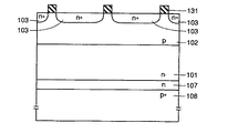
図1は、本願発明の実施の形態1における半導体装置の構成を示す概略断面図である。図1を参照して、本実施の形態の半導体装置は、たとえば50〜250μmの厚みt1を有する半導体基板に形成されたトレンチ型IGBTである。n-シリコン基板1は、たとえば約1×1014cm-3の濃度を有している。このn-シリコン基板1の第1主面側に、たとえば濃度が約1×10¹⁵〜1×1018cm-3で第1主面からの拡散深さが約1.0〜4.0μmのp型半導体よりなるp型ボディ領域2が形成されている。p型ボディ領域2内の第1主面には、たとえば濃度が1×10¹⁸〜1×1020cm-3で、第1主面からの拡散深さが約0.3〜2.0μmのn型半導体よりなるn型エミッタ領域3が形成されている。このn型エミッタ領域3と隣り合うように第1主面には、p型ボディ領域2への低抵抗コンタクトをとるためのp+不純物拡散領域6が、たとえば1×10¹⁸〜1×1020cm-3程度の濃度で、第1主面からの拡散深さがn型エミッタ領域3の深さ以下で形成されている。
Hereinafter, embodiments of the present invention will be described with reference to the drawings.
(Embodiment 1)
FIG. 1 is a schematic cross-sectional view showing the configuration of the semiconductor device according to the first embodiment of the present invention. Referring to FIG. 1, the semiconductor device of the present embodiment is a trench IGBT formed in a semiconductor substrate having a thickness t 1 of, for example, 50 to 250 μm. The n − silicon substrate 1 has a concentration of about 1 × 10 14 cm −3 , for example. On the first main surface side of the n − silicon substrate 1, for example, the concentration is about 1 × 10 15 to 1 × 10 18 cm −3 and the diffusion depth from the first main surface is about 1.0 to 4.0 μm. A p-
第1主面には、n型エミッタ領域3とp型ボディ領域2とを突抜けてn-シリコン基板1に達するゲート用溝1aが形成されている。このゲート用溝1aは、第1主面からたとえば3〜10μmの深さを有しており、ゲート用溝1aのピッチは、たとえば2.0μm〜6.0μmである。このゲート用溝1aの内表面には、ゲート絶縁膜4aが形成されている。このゲート絶縁膜4aは、たとえばゲート絶縁膜の特性、信頼性およびデバイス歩留りを向上させる目的で、CVD法により形成されたシリコン酸化膜と熱酸化法により形成されたシリコン酸化膜もしくは窒素がSi/SiO2界面に偏析しているシリコン窒化酸化膜との積層構造を有している。
Formed on the first main surface is a
ゲート用溝1a内を埋め込むように、たとえばリンが高濃度に導入された多結晶シリコンや、W/TiSi2などのメタル材料よりなるゲート電極5aが形成されている。なお、ゲート電極5aの低抵抗化のためにゲート電極5aの表面にシリサイド層(たとえばTiSi2、CoSiなど)が形成されていてもよい。このゲート電極5aの上面には、たとえばシリコン酸化膜よりなる絶縁膜22Aが形成されている。またゲート電極5aは、ゲート電位Gを与える制御電極に電気的に接続されている。
A
このようにゲート用溝1aとゲート絶縁膜4aとゲート電極5aとからゲートトレンチが構成されている。またn-シリコン基板1とn型エミッタ領域3とゲート電極5aとから、n-シリコン基板1をドレインとし、n型エミッタ領域3をソースとする絶縁ゲート型電界効果トランジスタ部(ここでは、MOSトランジスタ)が構成されている。このMOSトランジスタ部が第1主面には複数個配置されている。
As described above, the
第1主面上には、たとえばシリケートガラスよりなる絶縁膜9と、CVD法により形成されたシリコン酸化膜よりなる絶縁膜22Bとが形成されており、これらの絶縁膜9,22Bには第1主面に達するコンタクトホール9aが設けられている。コンタクトホール9aの内表面および絶縁膜9、22Bの上面に沿うようにバリアメタル層10が形成されている。このバリアメタル層10と半導体基板との接する部分にはシリサイド層21aが形成されている。このバリアメタル層10およびシリサイド層21aを介して、n型エミッタ領域3およびp+不純物拡散領域6には、エミッタ電位Eを与えるエミッタ電極11が電気的に接続されている。
On the first main surface, for example, an insulating
また、n-シリコン基板1の第2主面側にはp型コレクタ領域8が形成されており、このp型コレクタ領域8にはコレクタ電位Cを与えるコレクタ電極12が電気的に接続されている。このコレクタ電極12の材質は、たとえばアルミニウム化合物である。
A p-
本実施の形態では、半導体基板の厚みt1は50μm以上250μm以下である。
本実施の形態の半導体装置においては、たとえばインバータ接続時には、エミッタ電位を基準に、制御電極のゲート電位Gはオフ状態では−15Vに、オン状態では+15Vに設定されたパルス状の制御信号であり、コレクタ電極12のコレクタ電位Cはゲート電位Gに従って概ね電源電圧を飽和電圧との間の電圧とされる。
In the present embodiment, the thickness t 1 of the semiconductor substrate is not less than 50 μm and not more than 250 μm.
In the semiconductor device of the present embodiment, for example, when the inverter is connected, the gate potential G of the control electrode is a pulsed control signal set to −15V in the off state and + 15V in the on state with the emitter potential as a reference. The collector potential C of the
次に、本実施の形態の製造方法について説明する。
図2〜図11は、本発明の実施の形態1における半導体装置の製造方法を工程順に示す概略断面図である。まず図2を参照して、厚いn-シリコン基板1よりなる基板表面に、たとえばピーク濃度が1×10¹⁵〜1×1018cm-3、第1主面からの拡散深さが1.0〜4.0μmのp型ボディ領域2が形成される。次に、第1主面上に、マスク層31が形成される。
Next, the manufacturing method of this embodiment will be described.
2 to 11 are schematic cross-sectional views showing the method of manufacturing the semiconductor device according to the first embodiment of the present invention in the order of steps. First, referring to FIG. 2, a peak concentration of, for example, 1 × 10 15 to 1 × 10 18 cm −3 and a diffusion depth from the first main surface of 1.0 on the surface of a thick n − silicon substrate 1 are 1.0. A p-
図3を参照して、マスク層31がパターニングされる。このパターニングされたマスク層31をマスクとして、たとえばイオン注入などが施されることにより、p型ボディ領域2内の第1主面に表面濃度が1.0×10¹⁸〜1.0×1020cm-3、第1主面からの拡散深さが0.3〜2.0μmのn型エミッタ領域3が形成される。この後、マスク層31が除去される。
Referring to FIG. 3,
図4を参照して、第1主面上に、たとえば熱酸化により形成されたシリコン酸化膜32と、CVD法により形成されたシリコン酸化膜33とが順に形成される。このシリコン酸化膜32、33が、通常の写真製版技術およびエッチング技術によりパターニングされる。このパターニングされたシリコン酸化膜32、33をマスクとして半導体基板に異方性エッチングが施される。これにより、n型エミッタ領域3とp型ボディ領域2とを突抜けてn-シリコン基板1に達するゲート用溝1aが形成される。
Referring to FIG. 4, a
図5を参照して、等方性プラズマエッチングおよび犠牲酸化などの処理を行なうことにより、ゲート用溝1aの開口部と底部とが丸くなり、かつゲート用溝1aの側壁の凹凸が平坦化される。また上記の犠牲酸化により、ゲート用溝1aの内表面に犠牲酸化膜32aが熱酸化膜32と一体化するように形成される。このように等方性プラズマエッチングおよび犠牲酸化を施すことにより、ゲート用溝1aの内表面に形成されるゲート絶縁膜の特性を向上させることが可能となる。この後、酸化膜32、32a、33が除去される。
Referring to FIG. 5, by performing processing such as isotropic plasma etching and sacrificial oxidation, the opening and bottom of
図6を参照して、上記酸化膜の除去により、半導体基板の第1主面およびゲート用溝1aの内表面が露出する。
Referring to FIG. 6, by removing the oxide film, the first main surface of the semiconductor substrate and the inner surface of
図7を参照して、ゲート用溝1aの内表面および第1主面に沿うように、たとえばシリコン酸化膜よりなるゲート絶縁膜4aが形成される。ゲート用溝1a内を埋め込むように、たとえばリンが高濃度に導入された多結晶シリコンもしくは不純物の導入されていない多結晶シリコンにリンがイオン注入により導入された材料や、W(タングステン)/TiSi2(チタンシリサイド)などのメタル材料からなる導電層5が表面全面に形成される。
Referring to FIG. 7,
なおゲート絶縁膜4aとしては、ゲート絶縁膜としての特性、信頼性およびデバイス歩留まりを向上させる目的で、CVD法により形成したシリコン酸化膜と熱酸化により形成したシリコン酸化膜もしくは窒素がシリコンと酸化シリコンとの界面に偏析した窒化酸化膜とからなる積層構造が用いられることが好ましい。
As the
この後、通常の写真製版技術およびエッチング技術により、導電層5がパターニングされる。
Thereafter, the
図8を参照して、このパターニングにより、導電層がゲート用溝1a内に残存されてゲート電極5aが形成される。ここで、ゲート電極5aの低抵抗化のためにゲート電極5aの表面にシリサイド層(たとえばTiSi2、CoSiなど)が形成されてもよい。この後、ゲート電極5aの上面が酸化されることにより、たとえばシリコン酸化膜よりなる絶縁膜22Aが形成される。この後、たとえば第1主面における表面濃度が1.0×10¹⁸〜1.0×1020cm-3、第1主面からの拡散深さがn型エミッタ領域3よりも浅いp+不純物拡散領域6が形成される。
Referring to FIG. 8, by this patterning, the conductive layer remains in
図9を参照して、第1主面上にたとえばシリケートガラスよりなる絶縁膜9と、CVD法により形成したシリコン酸化膜よりなる絶縁膜22Bとが順に形成される。この絶縁膜9、22Bに、通常の写真製版技術およびエッチング技術によりコンタクトホール9aが形成される。
Referring to FIG. 9, an insulating
図10を参照して、たとえば金属層よりなるバリアメタル層10がスパッタリング法により形成される。この後、ランプアニールが施されてバリアメタル層10と半導体基板との接触部にシリサイド層21aが形成される。この後、エミッタ電極11が形成される。
Referring to FIG. 10,
図11を参照して、半導体基板の第2主面側のn-ドリフト層1が研磨される。この研磨により、半導体基板の厚みt1は50μm以上250μm以下に調整される。 Referring to FIG. 11, n − drift layer 1 on the second main surface side of the semiconductor substrate is polished. By this polishing, the thickness t 1 of the semiconductor substrate is adjusted to 50 μm or more and 250 μm or less.
研磨後の第2主面にたとえばイオン注入法によりp型不純物を注入した後に拡散などさせることにより、p型コレクタ領域8が形成され、さらにたとえばアルミニウム化合物よりなるコレクタ電極12が形成されて図1に示す半導体装置が完成する。
A p-
なお、本実施の形態においては、図11に示すようにエミッタ電極11を形成した後にドリフト層(n-層1)の第2主面を研磨する工程となっている。しかし、図9に示すようにコンタクトホール9aの開口後もしくは開口前にドリフト層(n-層1)の第2主面が研磨されて半導体基板の厚みが50μm以上250μm以下とされてもよい。
In the present embodiment, the second main surface of the drift layer (n − layer 1) is polished after the
また本実施の形態における半導体基板の厚みt1は、図75に示す従来例のn-シリコン層101の厚みt3よりも厚い。 Further, the thickness t 1 of the semiconductor substrate in the present embodiment is thicker than the thickness t 3 of the n − silicon layer 101 of the conventional example shown in FIG.
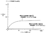
次に、本実施の形態において半導体基板の厚みを50μm以上250μm以下にした理由について説明する。 Next, the reason why the thickness of the semiconductor substrate is set to 50 μm or more and 250 μm or less in this embodiment will be described.
図12は、VCESあるいはVONと半導体基板の厚みとの関係を示す図である。図12を参照して、基板の濃度が高い場合には、VCESは50μmより小さい場合に急激に低下する。これにより、デバイス動作時の主耐圧を確保し難くなるため、半導体基板の厚みt1の下限値は50μmとした。 FIG. 12 is a diagram showing the relationship between V CES or V ON and the thickness of the semiconductor substrate. Referring to FIG. 12, when the concentration of the substrate is high, V CES rapidly decreases when it is smaller than 50 μm. This makes it difficult to ensure the main breakdown voltage during device operation, so the lower limit of the thickness t 1 of the semiconductor substrate is set to 50 μm.
また半導体基板の厚みt1が250μmより厚くなっても、基板の濃度が低い場合、VCESはほぼ一定値を示し、主耐圧の向上にあまり効果がないことがわかる。また、半導体基板の厚みt1が250μmを超えた場合、IGBTが動作する際の定常ロス(EDC)が急激に増加してしまう。以下、そのことについて説明する。 In addition, even when the thickness t 1 of the semiconductor substrate is greater than 250 μm, V CES shows a substantially constant value when the substrate concentration is low, and it can be seen that there is not much effect on the improvement of the main breakdown voltage. In addition, when the thickness t 1 of the semiconductor substrate exceeds 250 μm, the steady loss (E DC ) when the IGBT operates increases rapidly. This will be described below.
図13は、VCEあるいはICと時間との関係を示す図である。図13を参照して、一般的にパワーデバイスが誘導負荷で動作した(スイッチングした)際のロス(Etotal)は図中ハッチングで示された領域で表わされ、かつ以下の式で表わされる。 FIG. 13 is a diagram showing the relationship between V CE or I C and time. Referring to FIG. 13, in general, a loss (E total ) when a power device operates (switches) with an inductive load is represented by a hatched area in the figure and represented by the following equation. .
Etotal=ESW+EDC
ここで、EDCはデバイスがON状態でのロス(定常ロス)である。またESWはデバイスがON、OFFしたときのロスであり、以下の式で表わされる。
E total = E SW + E DC
Here, E DC is a loss (steady loss) when the device is in the ON state. E SW is a loss when the device is turned on and off, and is expressed by the following equation.
ESW=EON+EOFF
EONとはデバイスがONしたときのスイッチングロスであり、EOFFはデバイスがOFFしたときのスイッチングロスである。
E SW = E ON + E OFF
E ON is a switching loss when the device is turned on, and E OFF is a switching loss when the device is turned off.
上記式中の定常ロスEDCは、VONにより影響され、VONが高くなるに伴い上昇する。この定常ロスEDCは、通常、全体のロスEtotalの約20〜30%を占めている。しかし、半導体基板の厚みが厚くなり、VONが上昇すると、Etotalに占めるEDCの割合が上昇する。特に、VON=2.6V付近でEtotalに占めるEDCの割合が急激に上昇し、デバイスへ悪影響を及ぼす。ここで、VONが2.6Vにおける半導体基板の厚みt1は図12より、約250μmであることがわかる。このことは、図14において、半導体基板の厚みが250μmを越えると、全体のロスEtotalに対する定常ロスEDCが急激に増加していることからも分かる。 Steady loss E DC in the above formula is affected by V ON, increases with the V ON is increased. This steady loss E DC normally occupies about 20 to 30% of the total loss E total . However, as the thickness of the semiconductor substrate increases and V ON increases, the ratio of E DC to E total increases. In particular, the ratio of E DC to E total is rapidly increased around V ON = 2.6 V, which adversely affects the device. Here, it can be seen from FIG. 12 that the thickness t 1 of the semiconductor substrate when V ON is 2.6 V is about 250 μm. This can also be seen from FIG. 14 that when the thickness of the semiconductor substrate exceeds 250 μm, the steady loss E DC increases rapidly with respect to the total loss E total .
このようにVONを低くし、それによりロスEtotalを低減するために、半導体基板の厚みの上限を250μmとした。 Thus, in order to reduce V ON and thereby reduce loss E total , the upper limit of the thickness of the semiconductor substrate was set to 250 μm.
以上より、本実施の形態のように半導体基板の厚みt1を50μm以上250μm以下とすることにより、ON電圧(VON)、主耐圧(VCES)、ロス(Etotal)というデバイス特性への悪影響を及ぼさずに従来よりも半導体基板厚みの自由度が増加する効果が得られる。 From the above, by setting the thickness t 1 of the semiconductor substrate to 50 μm or more and 250 μm or less as in the present embodiment, the device characteristics such as ON voltage (V ON ), main withstand voltage (V CES ), and loss (E total ) are reduced. The effect of increasing the degree of freedom of the thickness of the semiconductor substrate can be obtained without adversely affecting the semiconductor substrate.
(実施の形態2)
図1を参照して、本実施の形態では、p型コレクタ領域8の不純物活性化率は50%以下である。
(Embodiment 2)
Referring to FIG. 1, in the present embodiment, the impurity activation rate of p-
なお、これ以外の構成については、上述した実施の形態1の構成とほぼ同じであるため、その説明を省略する。 Other configurations are substantially the same as the configuration of the first embodiment described above, and thus the description thereof is omitted.
また本実施の形態の製造方法は、上述した実施の形態1の製造方法とほぼ同じであるため、その説明も省略する。 Further, the manufacturing method of the present embodiment is substantially the same as the manufacturing method of the first embodiment described above, and therefore the description thereof is also omitted.
本実施の形態では、図1に示す各領域1、2、3、6が形成された後にp型コレクタ領域8がたとえばイオン注入などにより形成される。このため、p型コレクタ領域8は、各領域1、2、3、6中の不純物を拡散などさせるための高温の熱処理を受けることはない。このため、本実施の形態のp型コレクタ領域8の不純物活性化率を50%以下と低く留めることができる。
In the present embodiment, after each
これに対して、図76〜図85に示す従来の製造方法では、図76に示すように最初のプロセスから既にp型コレクタ領域108が存在している。このため、p型コレクタ領域108は製造プロセスにおけるすべての熱処理を受けることになる。よって、従来のp型コレクタ領域108はほぼ100%の不純物活性化率を有しており、これ以下の活性化率にすることは困難であった。
On the other hand, in the conventional manufacturing method shown in FIGS. 76 to 85, the p-
以上より、図15に示すように本実施の形態のp型コレクタ領域8の不純物活性化率は、従来例のp型コレクタ領域108の不純物活性化率(100%)と異なり、50%以下とすることができる。
From the above, as shown in FIG. 15, the impurity activation rate of the p-
なお図15は、図1の構成におけるp型コレクタ層の実際のイオン注入量(横軸)と有効ドーズ量(縦軸)との関係を示す図である。また、図15中における黒丸印は、図2〜図11の工程により形成された図1の構成におけるp型コレクタ領域8の不純物活性化率の測定データである。
FIG. 15 is a diagram showing the relationship between the actual ion implantation amount (horizontal axis) and the effective dose amount (vertical axis) of the p-type collector layer in the configuration of FIG. Further, black circles in FIG. 15 are measurement data of the impurity activation rate of the p-
次に、本実施の形態においてp型コレクタ領域8の不純物活性化率を50%以下とした理由について説明する。
Next, the reason why the impurity activation rate of the p-
図16はp型コレクタ層のイオン注入量(イオン注入時の注入量)とVONとの関係を示す図である。 FIG. 16 is a diagram showing the relationship between the ion implantation amount of the p-type collector layer (implantation amount during ion implantation) and V ON .
本実施の形態では、p型コレクタ領域8の不純物活性化率が50%以下と低くされているため、実際に設定したイオン注入量に対して形成されるp型コレクタ領域8の濃度変化を小さくすることができる。これにより、実際に設定したイオン注入量に対して熱処理後の実効的なp型コレクタ領域8の濃度の変動が小さくなる。つまり、設定値が変動した場合のマージンが大きくなる。このため、イオン注入時に注入量が変動しても、半導体基板中に形成されるp型コレクタ領域8が設計時の濃度を実現することが可能になる。
In this embodiment, since the impurity activation rate of the p-
図16を参照して、IGBTのp型コレクタ領域8の濃度はVON値に影響する。このVONは、p型コレクタ領域のイオン注入量が1×1014cm-2付近からイオン注入量が低くなるに伴い急激に上昇する。従来の100%の不純物活性化率を持つp型コレクタ領域108であれば、VONのコレクタ領域注入量に対する変動が大きく、かつ図15に示すイオン注入時にイオン注入量が変動した際の実効的なコレクタ領域の濃度変動が大きいため、イオン注入時にイオン注入量が変動した際のVONの変動が大きくなり、デバイス設計が困難となる。
Referring to FIG. 16, the concentration of IGBT p-
一方、本実施の形態の低い不純物活性化率を持つp型コレクタ領域8であれば、従来のコレクタ領域108が抱える上記問題を抑制する作用があり、デバイス設計に対して十分な自由度を持たせかつプロセス中の変動に対してもマージンが大きく、プロセス中の変動によるデバイス特性への悪影響を防止する作用がある。
On the other hand, the p-
(実施の形態3)
図17は、図1に示すXVII−XVII線に沿う部分に対応した不純物濃度プロファイルを示す図である。図17を参照して、実線は図1におけるコレクタ側の構造A、点線は後述する実施の形態4(図21)のコレクタ構造B、および一点鎖線は図75におけるコレクタ構造の各不純物プロファイルを示している。
(Embodiment 3)
FIG. 17 is a diagram showing an impurity concentration profile corresponding to a portion along line XVII-XVII shown in FIG. Referring to FIG. 17, the solid line indicates the collector-side structure A in FIG. 1, the dotted line indicates the collector structure B of the embodiment 4 (FIG. 21) described later, and the alternate long and short dash line indicates each impurity profile of the collector structure in FIG. ing.
図1におけるコレクタ側の構造Aにおいては、p型コレクタ領域8の第2主面における表面濃度は5×1015cm-3以上であり、p型コレクタ領域8の第2主面からの深さは1μm以下である。p型コレクタ領域8の拡散深さが浅いのは、他の不純物領域が形成された後にp型コレクタ領域8が形成されるためである。つまり、このp型コレクタ領域8が、他の不純物領域の形成のための高温の熱処理を受けないためである。
In the structure A on the collector side in FIG. 1, the surface concentration of the second main surface of the p-
またp型コレクタ領域8の第2主面における表面濃度を5×1015cm-3以上にすることにより、p型コレクタ領域8とコレクタ電極12との低抵抗なコンタクトを実現することができ、デバイス特性が不安定になることが防止できる。
Further, by setting the surface concentration of the second main surface of the p-
本実施の形態におけるp型コレクタ領域8の表面濃度を変化させた場合におけるVONとVCESに関するストレス印加後の経時変化を図18および図19に示す。図18および図19より、p型コレクタ領域8の表面濃度が5×1015cm-3未満の場合には、VON、VCESの経時変化が大きくなっている。このことより、p型コレクタ領域8の表面濃度が5×1015cm-3未満と低すぎるとデバイス特性の経時変化が大きくデバイス特性への悪影響を及ぼすことがわかる。よって、本実施の形態のコレクタ側の構造Aのように表面濃度を5×1015cm-3以上にすることで、デバイスの信頼性が低下することを抑制する効果があることがわかる。
FIG. 18 and FIG. 19 show the change over time after stress application regarding V ON and V CES when the surface concentration of the p-
また398Kの温度での主接合リーク特性(主接合はp型ボディ領域2とn-シリコン基板1との接合部)を図20に示す。図20より、図75に示す従来のコレクタ構造では、VCEが上昇するに伴いEOFFが急激に上昇することがわかる。一方、本実施の形態のコレクタ構造Aでは、VCEの変化によるEOFFの変化が小さく、デバイス動作時の電源電圧が変化した際のスイッチングロスの増加および変化を抑制する効果があることがわかる。
FIG. 20 shows main junction leakage characteristics at a temperature of 398 K (the main junction is the junction between the p-
これは、本実施の形態のコレクタ構造Aでは、従来のコレクタ構造に比べ、p型コレクタ領域8の第2主面における表面濃度が低く(または不純物活性化率が50%以下と低く)、かつ拡散深さが1μm以下と浅いため、VCEが上昇しても、デバイスがON時のコレクタ領域からのキャリア注入効率が従来のコレクタ構造より小さくなり、デバイスがOFF時にn-シリコン基板1に蓄積されたホールの量が少なくなるからである。 This is because the collector structure A of the present embodiment has a lower surface concentration at the second main surface of the p-type collector region 8 (or an impurity activation rate as low as 50% or less) compared to the conventional collector structure, and Since the diffusion depth is as shallow as 1 μm or less, even if V CE rises, the carrier injection efficiency from the collector region when the device is ON is smaller than the conventional collector structure, and it accumulates in the n − silicon substrate 1 when the device is OFF. This is because the amount of holes made is reduced.
(実施の形態4)
図21は、本発明の実施の形態4における半導体装置のコレクタ側の構成を示す概略断面図である。図21を参照して、本実施の形態の構成は、n-シリコン基板1がp型コレクタ領域8とpn接合を構成する領域付近に高濃度のn型不純物拡散領域7を有する点において図1に示す構成と異なる。本実施の形態のコレクタ側の構造Bにおけるn型不純物拡散領域7は、図17に示すようにp型コレクタ領域8の不純物濃度ピーク以下の濃度の不純物濃度ピークを有している。またn型不純物拡散領域7は第2主面からの深さが2μm以下となるように形成されている。
(Embodiment 4)
FIG. 21 is a schematic cross-sectional view showing the configuration on the collector side of the semiconductor device in the fourth embodiment of the present invention. Referring to FIG. 21, the configuration of the present embodiment is different from that shown in FIG. 1 in that n − silicon substrate 1 has a high-concentration n-type
なお、これ以外のp型コレクタ領域8およびMOSトランジスタ側の構造は実施の形態1〜3と同等の構成を有しているため、その説明を省略する。
Since the other structures on the p-
本実施の形態の製造方法においては、図11に示すようにドリフト層(n-層1)の第2主面が研磨された後に、第2主面にn型不純物拡散領域7が形成され、その後にp型コレクタ領域8が形成される。なお、これ以外の製造方法については、上述した実施の形態1の方法とほぼ同じであるため、その説明は省略する。
In the manufacturing method of the present embodiment, the n-type
本実施の形態において、n型不純物拡散領域7の拡散深さが浅くなるのは、MOSトランジスタ側の不純物領域が形成された後にn型不純物拡散領域7が形成されるため、MOSトランジスタ側の不純物領域の形成のための高温の熱処理をn型不純物拡散領域7が受けないからである。
In this embodiment, the n-type
本実施の形態のコレクタ構造Bは、図1に示すコレクタ構造Aより、p型コレクタ領域8からのホールの注入効率が抑制された構造である。
The collector structure B of the present embodiment is a structure in which the hole injection efficiency from the p-
本実施の形態では、n型不純物拡散領域7を設けたことにより、図1に示すコレクタ構造Aに比べて以下の効果が得られる。
In the present embodiment, by providing the n-type
(1) 図22に示すように主接合リーク特性が減少し、耐圧が上昇する。
(2) 図23に示すようにターンオフ時のICの波形でテール電流が少なくなり、その結果、スイッチングロス(EOFF)が低減する。
(1) As shown in FIG. 22, the main junction leakage characteristic decreases and the breakdown voltage increases.
(2) As shown in FIG. 23, the tail current is reduced in the waveform of I C at the time of turn-off, and as a result, the switching loss (E OFF ) is reduced.
また構造Bにおいても、p型コレクタ領域8が構造Aと同様の構成を有するため、図20に示すように、VCEの変化によるEOFFの変化を抑制する効果がある。
Also in the structure B, since the p-
(実施の形態5)
図24は、本発明の実施の形態5における半導体装置の構成を概略的に示す平面図である。また図25および図26は、図24のXXV−XXV線およびXXVI−XXVI線の各々に沿う概略断面図である。
(Embodiment 5)
FIG. 24 is a plan view schematically showing a configuration of the semiconductor device in the fifth embodiment of the present invention. 25 and 26 are schematic sectional views taken along lines XXV-XXV and XXVI-XXVI in FIG.
主に図25を参照して、本実施の形態においては、n-シリコン基板1がp型ボディ領域2とpn接合を構成する領域付近に比較的高濃度のn型不純物拡散領域14が設けられている。
Referring mainly to FIG. 25, in the present embodiment, a relatively high concentration n-type
主に図24を参照して、2本のゲート用溝1aに挟まれる第1主面には、p+不純物拡散領域6が図中上下方向に複数個(たとえば3個)に分けられている。この図中上下方向に分けられた各p+不純物拡散領域6は単一のコンタクトホール9aによりエミッタ電極11と電気的に接続されている。
Referring mainly to FIG. 24, a plurality of (for example, three) p +
主に図24および図26を参照して、ゲート用溝1a内を埋め込むゲート電極5aは、ゲート用溝1a外部の第1主面上にも延びており、その延びた部分においてパッドとなる導電層11と電気的に接続されている。このパッドとなる導電層11の下層にはバリアメタル層10が位置し、バリアメタル層10とゲート電極5aとが接する領域にシリサイド層21aが形成されている。
Referring mainly to FIGS. 24 and 26,
なお、このパッドなる導電層11およびエミッタ電極11上にパッシベーション膜15が形成されている。
A
なお、これ以外の構成については、上述した実施の形態1の構成とほぼ同じであるため、同一の部材については同一の符号を付し、その説明を省略する。 Since the configuration other than this is almost the same as the configuration of the first embodiment described above, the same members are denoted by the same reference numerals, and the description thereof is omitted.
n型不純物拡散領域14を設けた構成は、図24〜図26の構成に限定されず、たとえば図27および図28に示す構成であってもよい。つまり、エミッタトレンチが設けられた構成にn型不純物拡散領域14が設けられてもよい。
The structure provided with n-type
図27は、本発明の実施の形態5における半導体装置の変形例の構成を示す概略平面図であり、図28は図27のXXVIII−XXVIII線に沿う概略断面図である。 27 is a schematic plan view showing a configuration of a modification of the semiconductor device according to the fifth embodiment of the present invention, and FIG. 28 is a schematic cross-sectional view taken along line XXVIII-XXVIII in FIG.
図27および図28を参照して、2つのMOSトランジスタに挟まれる領域にエミッタトレンチが設けられている。エミッタトレンチは、エミッタ用溝1bと、エミッタ用絶縁膜4bと、エミッタ用導電層5bとから構成されている。エミッタ用溝1bは、p型ボディ領域2およびn型不純物拡散領域14を突き抜けてn-シリコン基板1に達している。エミッタ用絶縁膜4bは、このエミッタ用溝1bの内表面に沿うように形成されている。エミッタ用導電層5bは、エミッタ用溝1b内を埋め込むように形成されており、その上層のエミッタ電極11と電気的に接続されている。
27 and 28, an emitter trench is provided in a region sandwiched between two MOS transistors. The emitter trench includes an
エミッタ電極11の下層にはバリアメタル層10が形成されており、このバリアメタル層10とエミッタ用導電層5bとの間にはシリサイド層21bが形成されている。
A
2つのエミッタトレンチに挟まれる第1主面にはp型ボディ領域2への低抵抗コンタクトを取るためのp+不純物拡散領域6が形成されており、その上にはシリサイド層21aが形成されている。
A p +
このような構成において、n-シリコン基板1がp型ボディ領域2とpn接合を構成する領域付近に比較的高濃度のn型不純物拡散領域14が設けられている。
In such a configuration, a relatively high concentration n-type
なお、これ以外の構成については、上述した図24〜図26の構成とほぼ同じであるため、同一の部材については同一の符号を付し、その説明を省略する。 In addition, since it is as substantially the same as the structure of FIGS. 24-26 mentioned above about the structure other than this, the same code | symbol is attached | subjected about the same member and the description is abbreviate | omitted.
また図29および図30は、図27および図28の構成と比較して、エミッタトレンチの側壁であって、第1主面にn型不純物拡散領域3を追加した点において異なる。
29 and 30 differ from the configuration of FIGS. 27 and 28 in that an n-type
なおこれ以外の構成については図27および図28に示す構成とほぼ同じであるため、同一の部材については同一の符号を付しその説明を省略する。 Since the configuration other than this is almost the same as the configuration shown in FIGS. 27 and 28, the same members are denoted by the same reference numerals and the description thereof is omitted.
図27〜図30においては、エミッタ用溝1b内を埋め込む導電層5bがエミッタ電位となる場合について説明したが、この導電層5bはフローティング電位を有していてもよい。その構成を以下に説明する。
27 to 30, the case where the
図31および図32を参照して、溝1b内を埋め込む導電層5bがエミッタ電極11と電気的に分離されており、フローティングな電位を有している。この場合、溝1b内を埋め込む導電層5b上にはたとえばシリコン酸化膜よりなる絶縁膜22Aと、たとえばシリコンケートガラスよりなる絶縁膜9と、たとえばシリコン酸化膜よりなる絶縁膜22Bとが形成されている。
Referring to FIGS. 31 and 32,
なおこれ以外の構成については、図27および図28に示す構成とほぼ同じであるため、同一の部材については同一の符号を付し、その説明を省略する。 Since the configuration other than the above is substantially the same as the configuration shown in FIGS. 27 and 28, the same members are denoted by the same reference numerals, and the description thereof is omitted.
本実施の形態で設けられるn型不純物拡散領域14は、p型ボディ領域2が形成される前に図33に示すようにイオン注入および拡散により形成される。この後、p型ボディ領域2が形成され、さらに実施の形態1と同様の後工程を経ることにより本実施の形態の各種の半導体装置(図24〜図32)が製造される。
The n-type
また、MOSトランジスタ構造E(図28)、F(図30)、G(図32)の各々は、エミッタ電位もしくはフローティング電位のトレンチを有することにより、MOSトランジスタ構造C(図1)、D(図25)よりも実効的なゲート幅が少なくなっている。その結果、図34に示すように構造E、F、Gは、構造C、Dよりも流れる電流が少なく飽和電流を抑制する効果を有する。 Also, each of the MOS transistor structures E (FIG. 28), F (FIG. 30), and G (FIG. 32) has a trench having an emitter potential or a floating potential, so that the MOS transistor structures C (FIG. 1) and D (FIG. The effective gate width is smaller than that of 25). As a result, as shown in FIG. 34, the structures E, F, and G have an effect of suppressing the saturation current with less current flowing than the structures C and D.
さらに図35を参照して、構造E、F、Gは、構造C、Dよりも低電圧/低電流密度(図34の領域S2)のところでON電圧が大きくなる。MOSトランジスタ構造Cは、従来構造よりn-シリコン基板1が厚くp型コレクタ領域8からのホール注入効率が低いためON電圧が上昇する。またMOSトランジスタ構造DにおいてON電圧が低下するのは、コレクタ構造Aでn-シリコン基板1が厚くても、USP6,040,599に記載されたn型不純物拡散領域14によるホール蓄積効果があるからである。MOSトランジスタ構造Dでは、従来構造よりn-シリコン基板1が厚くても、ON電圧を低下させる効果がある。
Further, referring to FIG. 35, in the structures E, F, and G, the ON voltage becomes larger at the lower voltage / lower current density (region S2 in FIG. 34) than in the structures C and D. In the MOS transistor structure C, since the n − silicon substrate 1 is thicker than the conventional structure and the hole injection efficiency from the p-
図34に示すようにMOSトランジスタ構造E、F、Gでは、飽和電流が低くなる効果により、図36に示すようにデバイスが無負荷状態でスイッチングしたときに、従来構造やMOSトランジスタ構造C、Dよりも長い時間任意の電流を保持することができる。つまり、MOSトランジスタ構造E、F、Gでは、デバイスの飽和電流を抑え、かつ破壊耐量を向上させる効果がある。 As shown in FIG. 34, in the MOS transistor structures E, F and G, due to the effect of lowering the saturation current, when the device is switched in a no-load state as shown in FIG. An arbitrary current can be held for a longer time. That is, the MOS transistor structures E, F, and G are effective in suppressing the saturation current of the device and improving the breakdown tolerance.
さらに、ON電圧を下げる効果があるMOSトランジスタ構造Dでは図37および図38に示すように無負荷状態でのスイッチング時に発振現象が発生する。しかし、MOSトランジスタ構造E、F、Gでは、n型不純物拡散領域14が存在してもエミッタ電位もしくはフローティング電位になる導電層5bが存在することにより発振現象を防止する効果がある。
Further, in the MOS transistor structure D having an effect of reducing the ON voltage, an oscillation phenomenon occurs at the time of switching in a no-load state as shown in FIGS. However, the MOS transistor structures E, F, and G have an effect of preventing the oscillation phenomenon due to the presence of the
また、MOSトランジスタ構造E、F、Gの上述した有効な効果は、第2主面側のコレクタ構造が図1に示す構造Aの場合でも、かつ図21に示す構造Bの場合でも同等に得ることができる。 The above-described effective effects of the MOS transistor structures E, F, and G can be obtained equally when the collector structure on the second main surface side is the structure A shown in FIG. 1 and the structure B shown in FIG. be able to.
逆に、実施の形態1〜4に示したMOSトランジスタ構造Cを他のMOSトランジスタD〜Gのいずれに変更しても実施の形態1〜4と同様の効果が得られる。 On the contrary, even if the MOS transistor structure C shown in the first to fourth embodiments is changed to any of the other MOS transistors D to G, the same effect as the first to fourth embodiments can be obtained.
(実施の形態6)
図39〜図74は、実施の形態5と同じ効果が得られるMOSトランジスタ構造の各種の派生構造を示す概略断面図である。図39〜図74に示すどの構造でも、またそれらのMOSトランジスタ構造がコレクタ構造AまたはBのいずれと組合せられても、実施の形態5に示すMOSトランジスタ構造による効果を得ることができる。
(Embodiment 6)
39 to 74 are schematic cross-sectional views showing various derivative structures of the MOS transistor structure that can obtain the same effects as those of the fifth embodiment. 39-74, and any MOS transistor structure in combination with collector structure A or B can provide the effects of the MOS transistor structure shown in the fifth embodiment.
また、コレクタ構造AまたはBから得られる実施の形態1〜4の効果は、図39〜図73に示すどのMOSトランジスタ構造と組合せられても同様に得ることができる。 Further, the effects of the first to fourth embodiments obtained from the collector structure A or B can be obtained in the same manner even when combined with any MOS transistor structure shown in FIGS.
以下に、図39〜図74に示す各MOSトランジスタ構造について説明する。
図39に示す構成は、2つのMOSトランジスタ部に挟まれる領域にエミッタ電位となる1つのエミッタトレンチが設けられている点およびゲート用溝1aの一方側面にのみn型エミッタ領域3が形成されている点において図28に示す構成と異なる。
The MOS transistor structures shown in FIGS. 39 to 74 will be described below.
In the configuration shown in FIG. 39, an n-
図40に示す構成は、複数のエミッタ用溝1b内が、一体化された単一の層よりなるエミッタ用導電層5bによって埋め込まれている。またエミッタ用導電層5bは、シリサイド層21bを介して、バリアメタル層10とエミッタ電極11とに電気的に接続されている。このシリサイド層21bは各エミッタ用溝1b間を繋ぐブリッジ上に形成されている。またシリサイド層21bが形成された領域以外のエミッタ用導電層5b上には、絶縁膜22A、9、22Bが形成されている。
In the configuration shown in FIG. 40, the plurality of
これ以外の構成については、上述した図28に示す構成とほぼ同じであるため、同一の部材については同一の符号を付し、その説明を省略する。 Since the configuration other than this is substantially the same as the configuration shown in FIG. 28 described above, the same members are denoted by the same reference numerals, and the description thereof is omitted.
図41に示す構成は、エミッタ用溝1bの両側壁であって第1主面にn型不純物拡散領域3が追加されている点において図40に示す構成と異なる。
The configuration shown in FIG. 41 is different from the configuration shown in FIG. 40 in that the n-type
図42に示す構成は、エミッタ用溝1b内を埋め込む導電層5bがフローティング電位となっている点において図40の構成と異なる。この場合、導電層5bの全面上に絶縁膜22A、9、22Bが形成されており、導電層5bはエミッタ電極11と電気的に絶縁されている。
The configuration shown in FIG. 42 is different from the configuration shown in FIG. 40 in that the
図43に示す構成は、エミッタ用溝1bの両側壁であって第1主面にn型不純物拡散領域3が追加されている点において図39に示す構成と異なる。
The configuration shown in FIG. 43 is different from the configuration shown in FIG. 39 in that n-type
図44に示す構成は、エミッタ用導電層5bの上面がエミッタ用溝1bよりも上方に突出している点において図39に示す構成と異なる。この場合、エミッタ用導電層5bは、その一部表面上に形成されたシリサイド層21bを介して、バリアメタル層10およびエミッタ電極11と電気的に接続されている。またシリサイド層21bが形成された領域以外のエミッタ用導電層5b上には、絶縁膜22A、9、22Bが形成されている。
The configuration shown in FIG. 44 is different from the configuration shown in FIG. 39 in that the upper surface of the emitter
図45に示す構成は、エミッタ用溝1bの両側面であって第1主面にn型不純物拡散領域3が追加されている点において図44に示す構成と異なる。
The configuration shown in FIG. 45 is different from the configuration shown in FIG. 44 in that n-type
図46に示す構成は、p型ボディ領域2がゲート用溝1aの側壁付近にのみ形成されている点において図28に示す構成と異なる。
The configuration shown in FIG. 46 is different from the configuration shown in FIG. 28 in that p-
図47に示す構成は、p型ボディ領域2がゲート用溝1aの側壁付近にのみ形成されている点において図30に示す構成と異なる。
The configuration shown in FIG. 47 is different from the configuration shown in FIG. 30 in that p-
図48に示す構成は、エミッタ用溝1b内を埋め込む導電層5bがフローティング電位となっている点において図46に示す構成と異なる。この場合、導電層5b上には、絶縁膜22A、9、22Bが形成されている。
The configuration shown in FIG. 48 is different from the configuration shown in FIG. 46 in that the
図49に示す構成は、2つのゲートトレンチに挟まれる領域にのみp型ボディ領域2が形成されている点において図39に示す構成と異なる。
The configuration shown in FIG. 49 is different from the configuration shown in FIG. 39 in that p-
図50に示す構成は、p型ボディ領域2がゲート用溝1aの側壁付近にのみ形成されている点において図40に示す構成と異なる。
The configuration shown in FIG. 50 differs from the configuration shown in FIG. 40 in that p-
図51に示す構成は、p型ボディ領域2がゲート用溝1aの側壁付近にのみ形成されている点において図41に示す構成と異なる。
The configuration shown in FIG. 51 is different from the configuration shown in FIG. 41 in that p-
図52に示す構成は、p型ボディ領域2がゲート用溝1aの側壁付近にのみ形成されている点において図42に示す構成と異なる。
The configuration shown in FIG. 52 is different from the configuration shown in FIG. 42 in that p-
図53に示す構成は、エミッタ用溝1bの両側壁であって第1主面にn型不純物拡散領域3が追加されている点において図49に示す構成と異なる。
The configuration shown in FIG. 53 is different from the configuration shown in FIG. 49 in that the n-type
図54に示す構成は、2つのゲートトレンチに挟まれる領域にのみp型ボディ領域2が形成されている点において図44に示す構成と異なる。
The configuration shown in FIG. 54 is different from the configuration shown in FIG. 44 in that p-
図55に示す構成は、2つのゲートトレンチに挟まれる領域にのみp型ボディ領域2が形成されている点において図45に示す構成と異なる。
The configuration shown in FIG. 55 is different from the configuration shown in FIG. 45 in that p-
図56に示す構成は、図28においてエミッタトレンチが存在した領域にトレンチを形成せずに、上記のMOSトランジスタ構造E〜Gとゲート幅(W)が同じになるようにゲートトレンチを形成した構成、つまりゲートトレンチの間をエミッタ電位となるように任意の寸法まで広げた構成である。 The configuration shown in FIG. 56 is a configuration in which a gate trench is formed so as to have the same gate width (W) as the above MOS transistor structures E to G without forming a trench in the region where the emitter trench exists in FIG. In other words, this is a configuration in which the gap between the gate trenches is expanded to an arbitrary size so as to be the emitter potential.
この場合、2つのゲートトレンチに挟まれる第1主面にはp型ボディ領域との低抵抗コンタクトを取るためのp+不純物拡散領域6が延在している。このp+不純物拡散領域6およびn型エミッタ領域3と接するようにシリサイド層21aが形成されている。p+不純物拡散領域6およびn型エミッタ領域3は、このシリサイド層21aとバリアメタル層10とを介してエミッタ電極11に電気的に接続されている。
In this case, a p +
なお、これ以外の構成については、上述した図28の構成とほぼ同じであるため、同一の部材については同一の符号を付し、その説明を省略する。 Since the configuration other than this is substantially the same as the configuration of FIG. 28 described above, the same members are denoted by the same reference numerals and the description thereof is omitted.
図57に示す構成は、図39においてエミッタトレンチが存在した領域にトレンチを形成せずに、上記のMOSトランジスタ構造E〜Gとゲート幅が同じになるようにゲートトレンチを形成した構成、つまりゲートトレンチの間をエミッタ電位となるように任意の寸法まで広げた構成である。 The configuration shown in FIG. 57 is a configuration in which a gate trench is formed so as to have the same gate width as the above MOS transistor structures E to G without forming a trench in the region where the emitter trench exists in FIG. This is a configuration in which the space between the trenches is expanded to an arbitrary size so as to be an emitter potential.
この構成においてもゲートトレンチに挟まれる第1主面にp型ボディ領域への低抵抗コンタクトを取るためにp+不純物拡散領域6が延在している。このp+不純物拡散領域6およびn型エミッタ領域3と接するようにシリサイド層21aが形成されている。p+不純物拡散領域6およびn型エミッタ領域3は、このシリサイド層21aとバリアメタル層10とを介してエミッタ電極11に電気的に接続されている。
Also in this configuration, the p +
なお、これ以外の構成については、上述した図39の構成とほぼ同じであるため、同一の部材については同一の符号を付し、その説明を省略する。 Since the configuration other than this is almost the same as the configuration of FIG. 39 described above, the same members are denoted by the same reference numerals, and the description thereof is omitted.
図58は、p型ボディ領域2がゲート用溝1aの側壁付近にのみ形成されている点において図56に示す構成と異なる。
58 differs from the structure shown in FIG. 56 in that p-
図59に示す構成は、2つのゲートトレンチに挟まれる領域にのみp型ボディ領域2が形成されている点において図57に示す構成と異なる。
The configuration shown in FIG. 59 is different from the configuration shown in FIG. 57 in that p-
上記においては、ゲート電極5aの上面がゲート用溝1a内に位置する場合について説明したが、ゲート用溝1a上に突出していてもよい。ゲート電極5aの上面がゲート用溝1aの上面に突出した構成を図60〜図70に示す。
In the above description, the case where the upper surface of the
図60は図28に示す構成、図61は図30に示す構成、図62は図32に示す構成、図63は図39に示す構成、図64は図40に示す構成、図65は図51に示す構成、図66は図42に示す構成、図67は図53に示す構成、図68は図54に示す構成、図69は図55に示す構成、図70は図41に示す構成において、ゲート電極5aの上面がゲート用溝1a上に突出した構成に対応している。なお、図62に示す構成は、溝1b内を埋め込む導電層5bの上面も溝1b上に突出している。
FIG. 60 shows the configuration shown in FIG. 28, FIG. 61 shows the configuration shown in FIG. 30, FIG. 62 shows the configuration shown in FIG. 32, FIG. 63 shows the configuration shown in FIG. 66, the configuration shown in FIG. 42, the configuration shown in FIG. 53, the configuration shown in FIG. 68, the configuration shown in FIG. 54, the configuration shown in FIG. 69, the configuration shown in FIG. This corresponds to a configuration in which the upper surface of the
なお、上記においてはトレンチ型ゲート構造について説明したが、平面ゲート型のIGBTにおいても実施の形態1〜5の構成を適用することができる。図71〜図74は平面ゲート型IGBTの構成を示す概略断面図である。 Although the trench gate structure has been described above, the configurations of the first to fifth embodiments can be applied to a planar gate IGBT. 71 to 74 are schematic cross-sectional views showing the configuration of the planar gate type IGBT.
図71を参照して、平面ゲート型IGBTは、たとえば厚さが約50μm以上250μmの半導体基板に形成されている。たとえば濃度が1×1014cm-3のn-シリコン基板1の第1主面側には、p型半導体よりなるp型ボディ領域2が選択的に形成されている。p型ボディ領域2は、たとえば1×10¹⁵〜1×1018cm-3の濃度を有し、第1主面から約1.0〜4.0μmの拡散深さを有している。p型ボディ領域2内の第1主面には、たとえば濃度が1×10¹⁸〜1×1020cm-3以上で、第1主面からの拡散深さが約0.3〜2.0μmのn型半導体よりなるn型エミッタ領域3が形成されている。このn型エミッタ領域3の隣には、p型ボディ領域2への低抵抗コンタクトを取るためのp+不純物拡散領域6がたとえば1×10¹⁸〜1×1020cm-3程度で、第1主面からの拡散深さがn型エミッタ領域3の深さ以下で形成されている。
Referring to FIG. 71, the planar gate type IGBT is formed on a semiconductor substrate having a thickness of about 50 μm to 250 μm, for example. For example, a p-
n-シリコン基板1とn型エミッタ領域3とに挟まれるp型ボディ領域2と対向するように第1主面上にゲート絶縁膜4aを介してゲート電極5aが形成されている。
A
このn-シリコン基板1とn型エミッタ領域3とゲート電極5aにより、n-シリコン基板1をドレインとし、n型エミッタ領域3をソースとする絶縁ゲート型電界効果トランジスタ部(ここではMOSトランジスタ部)が構成されている。
By this n − silicon substrate 1, n
2つのMOSトランジスタ部に挟まれる第1主面上には、エミッタ電位となる導電層5bが形成されている。この導電層5bとゲート電極5aとの材質には、たとえばリンを高濃度に導入した多結晶シリコン、高融点金属材料、高融点金属シリサイドまたはそれらの複合膜が用いられる。
A
第1主面上には絶縁膜9が形成されており、この絶縁膜9には第1主面の一部表面に達するコンタクトホール9aが形成されている。このコンタクトホール9aの底部にはバリアメタル層10が形成されている。このバリアメタル層10を介して導電層5b、p+不純物拡散領域6およびn型エミッタ領域3とに、エミッタ電位Eを与えるエミッタ電極11が電気的に接続されている。
An insulating
またn-シリコン基板1の第2主面側には、n型不純物拡散領域7とp型コレクタ領域8とが順に形成されている。p型コレクタ領域8には、コレクタ電位Cを与えるコレクタ電極12が電気的に接続されている。このコレクタ電極12の材質は、たとえばアルミニウム化合物である。
An n-type
本実施の形態において、半導体基板の厚みt1は50μm以上250μm以下である。またp型コレクタ領域8の不純物活性化率は50%以下である。またp型コレクタ領域8の第2主面からの深さは1μm以下であることが好ましい。またn型不純物拡散領域7はp型コレクタ領域8の不純物濃度ピークよりも低い不純物濃度ピークを有していることが好ましい。またこのn型不純物拡散領域7は第2主面から2μm以下の深さで形成されていることが好ましい。
In the present embodiment, the thickness t 1 of the semiconductor substrate is not less than 50 μm and not more than 250 μm. The impurity activation rate of the p-
なお、図71の構成に対して、図72に示すようにn型不純物拡散領域14が追加されてもよく、また図73に示すようにn型不純物拡散領域7が省略されてもよく、また図74に示すようにn型不純物拡散領域14が追加されかつn型不純物拡散領域7が省略されてもよい。
71, the n-type
なお、本実施の形態においては、IGBTを例に挙げて説明したが、IGBTに限られず絶縁ゲート型電界効果トランジスタを有する素子であれば本発明を適用することができる。 In this embodiment, the IGBT is described as an example. However, the present invention is not limited to the IGBT and can be applied to any element having an insulated gate field effect transistor.
本発明は、高耐圧素子、とりわけIGBTの構造に関するものであり、特にトレンチゲートIGBTにおいては効果を最大に発揮するものである。また、本発明は、低ON電圧化を実現し、破壊耐量を確保するとともに、高電圧側でのスイッチングロスを低減できる半導体装置およびその製造方法に有利に適用され得る。またプロセス条件の変動によるデバイス特性への悪影響を防止できる半導体装置およびその製造方法にも有利に適用され得る。また基板厚みの自由度の制限が少なく、かつ低価格化に適した半導体装置の製造方法にも有利に適用され得る。 The present invention relates to a structure of a high breakdown voltage element, particularly an IGBT, and exhibits the maximum effect particularly in a trench gate IGBT. In addition, the present invention can be advantageously applied to a semiconductor device and a method for manufacturing the same that can achieve a low ON voltage, ensure breakdown resistance, and reduce switching loss on the high voltage side. Further, the present invention can be advantageously applied to a semiconductor device and a manufacturing method thereof that can prevent adverse effects on device characteristics due to variations in process conditions. Further, the present invention can be advantageously applied to a method for manufacturing a semiconductor device that is less restricted in the degree of freedom of substrate thickness and is suitable for lowering the price.
今回開示された実施の形態はすべての点で例示であって制限的なものではないと考えられるべきである。本発明の範囲は上記した説明ではなくて特許請求の範囲によって示され、特許請求の範囲と均等の意味および範囲内でのすべての変更が含まれることが意図される。 The embodiment disclosed this time should be considered as illustrative in all points and not restrictive. The scope of the present invention is defined by the terms of the claims, rather than the description above, and is intended to include any modifications within the scope and meaning equivalent to the terms of the claims.
1 シリコン基板(ドリフト層)、1a ゲート用溝、1b エミッタ用溝、2 p型ボディ領域、3 n型エミッタ領域、4a ゲート絶縁膜、4b エミッタ用絶縁膜、5 導電層、5a ゲート電極、5b エミッタ用導電層、6 不純物拡散領域、7 n型不純物拡散領域、8 p型コレクタ領域、9,22A,22B 絶縁膜、9a コンタクトホール、10 バリアメタル層、11 エミッタ電極、12 コレクタ電極、14 n型不純物拡散領域、15 パッシベーション膜、21a,21b シリサイド層、31 マスク層、32 酸化膜、32a 犠牲酸化膜、33 シリコン酸化膜。 1 silicon substrate (drift layer), 1a gate groove, 1b emitter groove, 2 p-type body region, 3 n-type emitter region, 4a gate insulating film, 4b emitter insulating film, 5 conductive layer, 5a gate electrode, 5b Conductive layer for emitter, 6 impurity diffusion region, 7 n-type impurity diffusion region, 8 p-type collector region, 9, 22A, 22B insulating film, 9a contact hole, 10 barrier metal layer, 11 emitter electrode, 12 collector electrode, 14 n Type impurity diffusion region, 15 passivation film, 21a, 21b silicide layer, 31 mask layer, 32 oxide film, 32a sacrificial oxide film, 33 silicon oxide film.
Claims (36)
前記第1主面側に絶縁ゲート構造を有し、かつ前記第1主面と前記第2主面との間で主電流が流れる絶縁ゲート型電界効果トランジスタ部を含む素子とを備え、
前記絶縁ゲート型電界効果トランジスタ部のゲート電極(5a)は、前記半導体基板の前記第1主面に設けられたゲート用溝(1a)内に形成されており、
前記半導体基板の厚みが50μm以上250μm以下である、半導体装置。 A semiconductor substrate having a first main surface and a second main surface facing each other;
An element having an insulated gate structure on the first main surface side and including an insulated gate field effect transistor portion in which a main current flows between the first main surface and the second main surface;
The gate electrode (5a) of the insulated gate field effect transistor portion is formed in a gate groove (1a) provided on the first main surface of the semiconductor substrate,
A semiconductor device, wherein the semiconductor substrate has a thickness of 50 μm or more and 250 μm or less.
前記第1導電型のソース拡散層(3)は前記第1主面に形成され、かつ第2導電型のボディ領域(2)を挟んで前記ドレイン拡散層(1)と対向していることを特徴とする、請求項1記載の半導体装置。 The insulated gate field effect transistor section has a source diffusion layer (3) and a drain diffusion layer (1) of the first conductivity type,
The first conductivity type source diffusion layer (3) is formed on the first main surface and faces the drain diffusion layer (1) with the second conductivity type body region (2) interposed therebetween. The semiconductor device according to claim 1, wherein the semiconductor device is characterized.
前記不純物拡散層(8)の前記第2主面における不純物表面濃度は、5×1015cm-3以上であることを特徴とする、請求項2記載の半導体装置。 A second conductivity type impurity diffusion layer (8) formed on the second main surface;
3. The semiconductor device according to claim 2, wherein an impurity surface concentration of the second main surface of the impurity diffusion layer is not less than 5 × 10 15 cm −3 .
前記ドレイン拡散層(1)は前記不純物拡散層(8)と接する領域に第1導電型の第1の高濃度領域(7)を有しており、
前記第1の高濃度領域(7)は、前記不純物拡散層(8)の不純物濃度ピーク以下の濃度の不純物濃度ピークを有していることを特徴とする、請求項3記載の半導体装置。 The impurity diffusion layer (8) and the drain diffusion layer (1) constitute a pn junction,
The drain diffusion layer (1) has a first conductivity type first high concentration region (7) in a region in contact with the impurity diffusion layer (8),
The semiconductor device according to claim 3, wherein the first high concentration region (7) has an impurity concentration peak having a concentration equal to or lower than an impurity concentration peak of the impurity diffusion layer (8).
複数個の前記ソース側電極用溝(1b)内を埋め込む前記導電層(5b)の各々は単一の層により一体的に形成されていることを特徴とする、請求項11記載の半導体装置。 A plurality of source-side electrode grooves (1b) are provided;
12. The semiconductor device according to claim 11, wherein each of the conductive layers (5b) filling the plurality of source-side electrode trenches (1b) is integrally formed by a single layer.
前記第1主面側に絶縁ゲート構造を有し、かつ前記第1主面と前記第2主面との間で主電流が流れる絶縁ゲート型電界効果トランジスタ部を含む素子とを備え、
前記絶縁ゲート型電界効果トランジスタ部は前記半導体基板に形成された第1導電型のドレイン拡散層(1)を有し、
前記素子は、前記ドレイン拡散層(1)と前記第2主面との間において前記ドレイン拡散層(1)とpn接合を構成するように前記第2主面に形成され、かつ不純物活性化率が50%以下の第2導電型の不純物拡散層(8)を有する、半導体装置。 A semiconductor substrate having a first main surface and a second main surface facing each other;
An element having an insulated gate structure on the first main surface side and including an insulated gate field effect transistor portion in which a main current flows between the first main surface and the second main surface;
The insulated gate field effect transistor unit has a drain diffusion layer (1) of a first conductivity type formed on the semiconductor substrate,
The element is formed on the second main surface so as to form a pn junction with the drain diffusion layer (1) between the drain diffusion layer (1) and the second main surface, and an impurity activation rate. A semiconductor device having a second conductivity type impurity diffusion layer (8) of 50% or less.
前記ドレイン拡散層(1)は前記不純物拡散層(8)と接する領域に第1導電型の第1の高濃度領域(7)を有しており、
前記第1の高濃度領域(7)は、前記不純物拡散層(8)の不純物濃度ピーク以下の濃度の不純物濃度ピークを有していることを特徴とする、請求項14記載の半導体装置。 The impurity diffusion layer (8) and the drain diffusion layer (1) of the insulated gate field effect transistor portion constitute a pn junction,
The drain diffusion layer (1) has a first conductivity type first high concentration region (7) in a region in contact with the impurity diffusion layer (8),
15. The semiconductor device according to claim 14, wherein the first high-concentration region (7) has an impurity concentration peak having a concentration equal to or lower than the impurity concentration peak of the impurity diffusion layer (8).
複数個の前記ソース側電極用溝(1b)内を埋め込む前記導電層(5b)の各々は単一の層により一体的に形成されていることを特徴とする、請求項22記載の半導体装置。 A plurality of source-side electrode grooves (1b) are provided;
23. The semiconductor device according to claim 22, wherein each of the conductive layers (5b) filling the plurality of source-side electrode trenches (1b) is integrally formed of a single layer.
前記半導体基板の前記第1主面に第2導電型のボディ領域(2)を形成する工程と、
前記ボディ領域(2)内の前記第1主面に第1導電型のソース拡散層(3)を形成する工程と、
前記半導体基板の前記第1主面にゲート用溝(1a)を形成する工程と、
ドレイン拡散層(1)となる前記半導体基板の第1導電型領域と前記ソース拡散層(3)とに挟まれる前記ボディ領域(2)にゲート絶縁膜(4a)を介して対向するように前記ゲート用溝(1a)内にゲート電極(5a)を形成する工程と、
前記ドレイン拡散層(1)と前記ソース拡散層(3)と前記ゲート電極(5a)とを有する絶縁ゲート型電界効果トランジスタ部を形成した後に、前記ドレイン拡散層(1)の前記第2主面を除去して前記半導体基板の厚みを50μm以上250μm以下にする工程とを有する、半導体装置の製造方法。 Preparing a first conductivity type semiconductor substrate having a first main surface and a second main surface facing each other;
Forming a second conductivity type body region (2) on the first main surface of the semiconductor substrate;
Forming a first conductivity type source diffusion layer (3) on the first main surface in the body region (2);
Forming a gate groove (1a) in the first main surface of the semiconductor substrate;
The body region (2) sandwiched between the first conductivity type region of the semiconductor substrate to be the drain diffusion layer (1) and the source diffusion layer (3) is opposed to the body region (2) via the gate insulating film (4a). Forming a gate electrode (5a) in the gate groove (1a);
After forming an insulated gate field effect transistor portion having the drain diffusion layer (1), the source diffusion layer (3), and the gate electrode (5a), the second main surface of the drain diffusion layer (1) And a step of removing the substrate to make the thickness of the semiconductor substrate 50 μm or more and 250 μm or less.
前記不純物拡散層(8)は、前記高濃度領域(7)とpn接合を構成するように前記第2主面に形成され、
前記高濃度領域(7)は、前記不純物拡散層(8)の不純物濃度ピーク以下の濃度の不純物濃度ピークを有していることを特徴とする、請求項26記載の半導体装置の製造方法。 The method further includes forming a first conductivity type high concentration region (7) having a higher impurity concentration than the drain diffusion layer (1) on the polished second main surface of the drain diffusion layer (1). ,
The impurity diffusion layer (8) is formed on the second main surface so as to form a pn junction with the high concentration region (7),
27. The method of manufacturing a semiconductor device according to claim 26, wherein the high concentration region (7) has an impurity concentration peak having a concentration equal to or lower than an impurity concentration peak of the impurity diffusion layer (8).
前記ソース側電極(11)に電気的に接続された導電層(5b)が前記ソース側電極用溝(1b)内を埋め込むように形成されることを特徴とする、請求項34記載の半導体装置の製造方法。 Forming a source-side electrode groove (1b) in the first main surface of the semiconductor substrate;
35. The semiconductor device according to claim 34, wherein a conductive layer (5b) electrically connected to the source side electrode (11) is formed so as to be embedded in the source side electrode trench (1b). Manufacturing method.
複数個の前記ソース側電極用溝(1b)内を埋め込むように前記ソース側電極用導電層が前記第1主面上に形成された後にパターニングされることにより、複数個の前記ソース側電極用溝(1b)内を埋め込む前記導電層(5b)の各々が単一の層により一体的に形成されることを特徴とする、請求項35記載の半導体装置の製造方法。 A plurality of the source side electrode grooves (1b) are formed,
The source-side electrode conductive layer is formed on the first main surface so as to be embedded in the plurality of source-side electrode trenches (1b), and then patterned, whereby the plurality of source-side electrode conductive layers are patterned. 36. The method of manufacturing a semiconductor device according to claim 35, wherein each of the conductive layers (5b) filling the groove (1b) is integrally formed by a single layer.
Priority Applications (1)
| Application Number | Priority Date | Filing Date | Title |
|---|---|---|---|
| JP2012102877A JP6026767B2 (en) | 2012-04-27 | 2012-04-27 | Semiconductor device and manufacturing method thereof |
Applications Claiming Priority (1)
| Application Number | Priority Date | Filing Date | Title |
|---|---|---|---|
| JP2012102877A JP6026767B2 (en) | 2012-04-27 | 2012-04-27 | Semiconductor device and manufacturing method thereof |
Related Parent Applications (1)
| Application Number | Title | Priority Date | Filing Date |
|---|---|---|---|
| JP2002555085A Division JP5025071B2 (en) | 2001-02-01 | 2001-02-01 | Semiconductor device and manufacturing method thereof |
Publications (2)
| Publication Number | Publication Date |
|---|---|
| JP2012165018A true JP2012165018A (en) | 2012-08-30 |
| JP6026767B2 JP6026767B2 (en) | 2016-11-16 |
Family
ID=46844035
Family Applications (1)
| Application Number | Title | Priority Date | Filing Date |
|---|---|---|---|
| JP2012102877A Expired - Lifetime JP6026767B2 (en) | 2012-04-27 | 2012-04-27 | Semiconductor device and manufacturing method thereof |
Country Status (1)
| Country | Link |
|---|---|
| JP (1) | JP6026767B2 (en) |
Cited By (3)
| Publication number | Priority date | Publication date | Assignee | Title |
|---|---|---|---|---|
| WO2017033315A1 (en) * | 2015-08-26 | 2017-03-02 | 三菱電機株式会社 | Semiconductor element |
| JP2021077911A (en) * | 2021-02-08 | 2021-05-20 | 三菱電機株式会社 | Semiconductor device, semiconductor device manufacturing method, and power conversion device |
| WO2024034277A1 (en) * | 2022-08-09 | 2024-02-15 | 富士電機株式会社 | Silicon carbide semiconductor device |
Citations (4)
| Publication number | Priority date | Publication date | Assignee | Title |
|---|---|---|---|---|
| JPH07321304A (en) * | 1994-05-20 | 1995-12-08 | Fuji Electric Co Ltd | Insulated gate bipolar transistor and its manufacture |
| JPH08316479A (en) * | 1995-03-14 | 1996-11-29 | Mitsubishi Electric Corp | Insulated-gate type semiconductor device and manufacture thereof |
| JPH11274484A (en) * | 1998-03-23 | 1999-10-08 | Toshiba Corp | Semiconductor device and its manufacturing method |
| WO2000035022A1 (en) * | 1998-12-04 | 2000-06-15 | General Electric Company | Insulated gate bipolar transistor for zero-voltage switching |
-
2012
- 2012-04-27 JP JP2012102877A patent/JP6026767B2/en not_active Expired - Lifetime
Patent Citations (5)
| Publication number | Priority date | Publication date | Assignee | Title |
|---|---|---|---|---|
| JPH07321304A (en) * | 1994-05-20 | 1995-12-08 | Fuji Electric Co Ltd | Insulated gate bipolar transistor and its manufacture |
| JPH08316479A (en) * | 1995-03-14 | 1996-11-29 | Mitsubishi Electric Corp | Insulated-gate type semiconductor device and manufacture thereof |
| JPH11274484A (en) * | 1998-03-23 | 1999-10-08 | Toshiba Corp | Semiconductor device and its manufacturing method |
| WO2000035022A1 (en) * | 1998-12-04 | 2000-06-15 | General Electric Company | Insulated gate bipolar transistor for zero-voltage switching |
| JP2002532886A (en) * | 1998-12-04 | 2002-10-02 | ゼネラル・エレクトリック・カンパニイ | Insulated gate bipolar transistor |
Cited By (5)
| Publication number | Priority date | Publication date | Assignee | Title |
|---|---|---|---|---|
| WO2017033315A1 (en) * | 2015-08-26 | 2017-03-02 | 三菱電機株式会社 | Semiconductor element |
| JPWO2017033315A1 (en) * | 2015-08-26 | 2018-04-19 | 三菱電機株式会社 | Semiconductor element |
| JP2021077911A (en) * | 2021-02-08 | 2021-05-20 | 三菱電機株式会社 | Semiconductor device, semiconductor device manufacturing method, and power conversion device |
| JP7090760B2 (en) | 2021-02-08 | 2022-06-24 | 三菱電機株式会社 | Semiconductor devices, semiconductor device manufacturing methods, and power conversion devices |
| WO2024034277A1 (en) * | 2022-08-09 | 2024-02-15 | 富士電機株式会社 | Silicon carbide semiconductor device |
Also Published As
| Publication number | Publication date |
|---|---|
| JP6026767B2 (en) | 2016-11-16 |
Similar Documents
| Publication | Publication Date | Title |
|---|---|---|
| JP5025071B2 (en) | Semiconductor device and manufacturing method thereof | |
| KR101191281B1 (en) | Semiconductor device | |
| JP4785334B2 (en) | Semiconductor device | |
| JP5452195B2 (en) | Semiconductor device and power conversion device using the same | |
| US7417296B2 (en) | Dielectric isolation type semiconductor device | |
| JP5908524B2 (en) | Semiconductor device | |
| US20130020634A1 (en) | Semiconductor Device and Electric Power Conversion System Using The Same | |
| TW200832700A (en) | Semiconductor device | |
| JP6026767B2 (en) | Semiconductor device and manufacturing method thereof | |
| US10134887B2 (en) | Semiconductor device and manufacturing method thereof | |
| JP6280148B2 (en) | Semiconductor device | |
| JP2016039320A (en) | Semiconductor device and method of manufacturing the same | |
| KR20110125585A (en) | Method for manufacturing dielectric isolation type semiconductor device | |
| JP2004006555A (en) | Semiconductor device | |
| JP5597963B2 (en) | Semiconductor device | |
| WO2016114043A1 (en) | Semiconductor device and method for manufacturing same | |
| JP6513168B2 (en) | Semiconductor device | |
| JP2010056212A (en) | Semiconductor integrated circuit device and method of manufacturing the same | |
| CN111295765B (en) | Semiconductor device with a plurality of semiconductor chips | |
| JP2020004864A (en) | Semiconductor device |
Legal Events
| Date | Code | Title | Description |
|---|---|---|---|
| A131 | Notification of reasons for refusal |
Free format text: JAPANESE INTERMEDIATE CODE: A131 Effective date: 20130820 |
|
| A521 | Written amendment |
Free format text: JAPANESE INTERMEDIATE CODE: A523 Effective date: 20131016 |
|
| A131 | Notification of reasons for refusal |
Free format text: JAPANESE INTERMEDIATE CODE: A131 Effective date: 20131112 |
|
| A521 | Written amendment |
Free format text: JAPANESE INTERMEDIATE CODE: A523 Effective date: 20140106 |
|
| A02 | Decision of refusal |
Free format text: JAPANESE INTERMEDIATE CODE: A02 Effective date: 20140819 |
|
| A521 | Written amendment |
Free format text: JAPANESE INTERMEDIATE CODE: A523 Effective date: 20141112 |
|
| A911 | Transfer to examiner for re-examination before appeal (zenchi) |
Free format text: JAPANESE INTERMEDIATE CODE: A911 Effective date: 20141119 |
|
| A912 | Re-examination (zenchi) completed and case transferred to appeal board |
Free format text: JAPANESE INTERMEDIATE CODE: A912 Effective date: 20150116 |
|
| A521 | Written amendment |
Free format text: JAPANESE INTERMEDIATE CODE: A523 Effective date: 20160426 |
|
| A61 | First payment of annual fees (during grant procedure) |
Free format text: JAPANESE INTERMEDIATE CODE: A61 Effective date: 20161013 |
|
| R150 | Certificate of patent or registration of utility model |
Ref document number: 6026767 Country of ref document: JP Free format text: JAPANESE INTERMEDIATE CODE: R150 |
|
| R250 | Receipt of annual fees |
Free format text: JAPANESE INTERMEDIATE CODE: R250 |
|
| R250 | Receipt of annual fees |
Free format text: JAPANESE INTERMEDIATE CODE: R250 |
|
| EXPY | Cancellation because of completion of term |