JP2012139655A - Printing apparatus - Google Patents
Printing apparatus Download PDFInfo
- Publication number
- JP2012139655A JP2012139655A JP2011000391A JP2011000391A JP2012139655A JP 2012139655 A JP2012139655 A JP 2012139655A JP 2011000391 A JP2011000391 A JP 2011000391A JP 2011000391 A JP2011000391 A JP 2011000391A JP 2012139655 A JP2012139655 A JP 2012139655A
- Authority
- JP
- Japan
- Prior art keywords
- semiconductor substrate
- printing apparatus
- unit
- relative movement
- head
- Prior art date
- Legal status (The legal status is an assumption and is not a legal conclusion. Google has not performed a legal analysis and makes no representation as to the accuracy of the status listed.)
- Withdrawn
Links
Images


Abstract
Description
本発明は、印刷装置に関するものである。 The present invention relates to a printing apparatus.
近年、紫外線照射によって硬化する紫外線硬化型インクを用いて記録媒体に画像またはパターンを形成する液滴吐出装置が注目されている。紫外線硬化型インクは、紫外線を照射するまでは硬化が非常に遅く、紫外線を照射すると急速に硬化するという、印刷インクとして好ましい特性を有する。また、硬化にあたって溶剤を揮発させることがないので、環境負荷が小さいという利点もある。 In recent years, attention has been focused on a droplet discharge device that forms an image or a pattern on a recording medium using ultraviolet curable ink that is cured by ultraviolet irradiation. The ultraviolet curable ink has a preferable characteristic as a printing ink, in which the curing is very slow until it is irradiated with ultraviolet rays, and it is rapidly cured when irradiated with ultraviolet rays. Moreover, since the solvent is not volatilized during curing, there is an advantage that the environmental load is small.
さらに、紫外線硬化型インクは、ビヒクルの組成により種々の記録媒体に高い付着性を発揮する。また、硬化した後は化学的に安定で、接着性、耐薬剤性、耐候性、耐摩擦性等が高く、屋外環境にも耐える等、優れた特性を有する。このため、紙、樹脂フィルム、金属箔等の薄いシート状の記録媒体の他、記録媒体のレーベル面、テキスタイル製品等、ある程度立体的な表面形状を有するものに対しても画像を形成できる。 Further, the ultraviolet curable ink exhibits high adhesion to various recording media depending on the composition of the vehicle. Further, after curing, it is chemically stable, has high adhesiveness, chemical resistance, weather resistance, friction resistance, etc., and has excellent characteristics such as withstand outdoor environments. For this reason, an image can be formed not only on a thin sheet-like recording medium such as paper, a resin film, or a metal foil, but also on a recording medium having a three-dimensional surface shape such as a label surface or a textile product.
ところで、例えば特許文献1に示すように、UVランプなどのUV照射手段がインクジェットヘッドの横に設けられているインクジェットプリンターを適用する場合、インクジェットヘッドによる描画位置近傍で描画直後にUVインクを硬化させることができる。
また、特許文献2には、走査方向に吐出ヘッドを複数配置することで、生産効率を向上させる技術が開示されている。
By the way, as shown in
しかしながら、上述したような従来技術には、以下のような問題が存在する。
吐出ヘッドから吐出されて記録媒体に塗布された紫外線硬化型インクがUV光を照射されて硬化(ピニング)するまでの時間(以下、ピニング時間と称する)が吐出ヘッド毎に異なるため、形成された膜の密着性、滲み方、着弾径等に差が生じて印刷品質が低下する虞がある。
However, the following problems exist in the conventional technology as described above.
The time until the ultraviolet curable ink discharged from the discharge head and applied to the recording medium is cured by being irradiated with UV light (hereinafter referred to as “pinning”) differs depending on the discharge head. There may be a difference in film adhesion, bleeding, landing diameter, and the like, resulting in a decrease in print quality.
本発明は、以上のような点を考慮してなされたもので、印刷品質の低下を招くことなく生産効率の向上に寄与できる印刷装置を提供することを目的とする。 The present invention has been made in consideration of the above points, and an object of the present invention is to provide a printing apparatus that can contribute to an improvement in production efficiency without causing a decrease in print quality.
上記の目的を達成するために本発明は、以下の構成を採用している。
本発明の印刷装置は、基材に対して相対移動して、活性光線で硬化する液体の液滴を吐出する吐出ヘッドと、該吐出ヘッドに対して前記相対移動方向後方側に設けられ前記基材上の前記液滴に前記活性光線を照射する照射部とを備え、前記吐出ヘッドは、前記相対移動方向と直交する方向に沿って複数設けられることを特徴とするものである。
In order to achieve the above object, the present invention employs the following configuration.
The printing apparatus of the present invention includes a discharge head that discharges liquid droplets that are relatively moved with respect to a substrate and are cured with actinic rays, and the base provided on the rear side in the relative movement direction with respect to the discharge head. An irradiating section that irradiates the droplets on the material with the actinic rays, and a plurality of the ejection heads are provided along a direction orthogonal to the relative movement direction.
従って、本発明の印刷装置は、複数の吐出ヘッドから液滴を吐出することで、生産効率を向上させつつ、相対移動方向で各吐出ヘッドと照射部との距離を同一とすることが可能になるため、吐出ヘッド毎のピニング時間が一定になり、吐出した液滴により形成される膜を一定状態とすることで印刷品質を確保できる。 Therefore, the printing apparatus of the present invention can discharge droplets from a plurality of discharge heads, thereby improving the production efficiency and making the distance between each discharge head and the irradiation unit the same in the relative movement direction. Therefore, the pinning time for each ejection head is constant, and the print quality can be ensured by keeping the film formed by the ejected droplets in a constant state.
上記の構成においては、前記吐出ヘッドが、前記液滴を吐出する複数のノズルが前記相対移動方向と交差する方向に沿って配置されたノズル列を有し、前記ノズル列のうち、前記基材に対して前記液滴を吐出するノズルで構成される実ノズル列の前記直交する方向の長さをLNとし、隣り合う前記吐出ヘッド同士の前記実ノズル列間の前記直交する方向の距離をLHとすると、隣り合う前記吐出ヘッドは、LH=n×LN(nは正の整数)を満足する位置関係で配置される構成を好適に採用できる。 In the above configuration, the ejection head includes a nozzle row in which a plurality of nozzles that eject the liquid droplets are arranged along a direction intersecting the relative movement direction, and the base material is included in the nozzle row. LN is the length in the orthogonal direction of an actual nozzle row composed of nozzles that discharge the droplets, and LH is the distance in the orthogonal direction between the actual nozzle rows of the adjacent ejection heads. Then, the structure which arrange | positions the said adjacent ejection head by the positional relationship which satisfies LH = n * LN (n is a positive integer) can be employ | adopted suitably.
これにより、本発明では、相対移動方向の液滴吐出動作と、複数の吐出ヘッドを相対移動方向と交差する方向に沿って距離LNフィードする動作とをn回繰り返すことにより、効率的に基材上に液滴を塗布することが可能になる。 Accordingly, in the present invention, the droplet discharge operation in the relative movement direction and the operation of feeding the plurality of discharge heads by the distance LN along the direction intersecting the relative movement direction are repeated n times, thereby efficiently performing the base material. It is possible to apply droplets on top.
上記の構成において、前記ノズル列が、前記相対移動方向に間隔をあけて複数設けられる場合には、前記吐出ヘッドにおける前記ノズル列と前記照射部との間の前記相対移動方向の距離に応じて、前記相対移動速度を制御する制御部を有する構成を好適に採用できる。
これにより、本発明では、照射部との相対移動方向の距離がノズル列で異なる場合には、相対移動速度を制御することで、液滴が着弾してから活性光線を照射して硬化するまでのピニング時間を一定時間とすることが可能なり、印刷品質を確保できる。
In the above configuration, when a plurality of the nozzle rows are provided at intervals in the relative movement direction, according to the distance in the relative movement direction between the nozzle row and the irradiation unit in the ejection head. A configuration having a control unit for controlling the relative movement speed can be suitably employed.
As a result, in the present invention, when the distance in the relative movement direction with the irradiation unit is different in the nozzle row, the relative movement speed is controlled until the liquid droplets are landed and irradiated with actinic rays to be cured. The pinning time can be set to a certain time, and the print quality can be secured.
また、上記構成において、前記ノズル列が、前記相対移動方向に間隔をあけて複数設けられる場合には、前記相対移動方向に応じて、前記複数のノズル列から使用するノズル列を選択する選択部を有する構成を好適に採用できる。
これにより、本発明では、選択部がノズル列と照射部との相対移動方向の距離が複数の吐出ヘッド間で一定となるノズル列を選択部が選択することにより、複数の吐出ヘッド間でピニング時間を一定とすることができる。
In the above configuration, when a plurality of the nozzle rows are provided at intervals in the relative movement direction, a selection unit that selects a nozzle row to be used from the plurality of nozzle rows according to the relative movement direction. A configuration having the above can be suitably employed.
Thus, in the present invention, the selection unit selects the nozzle row in which the distance in the relative movement direction between the nozzle row and the irradiation unit is constant between the plurality of ejection heads, thereby pinning between the plurality of ejection heads. Time can be constant.
一方、本発明の印刷装置は、活性光線を照射し、且つ、所定方向に沿って並んで設けられた一対の照射部と、前記活性光線で硬化する液体の液滴を吐出する第1の吐出ヘッド及び第2の吐出ヘッドと、前記第1の吐出ヘッド、前記第2の吐出ヘッド及び前記照射部を前記所定方向に基材に対して相対的に移動させる移動手段と、を備え、前記前記第1の吐出ヘッド及び前記第2の吐出ヘッドは、前記所定方向と直交する方向に沿って並んで配置されることを特徴とする。
従って、本発明では、移動手段による基材に対する相対移動時に第1、第2の吐出ヘッドから液滴を吐出することで、生産効率を向上させつつ、相対移動方向で各吐出ヘッドと照射部との距離を同一とすることが可能になるため、吐出ヘッド毎のピニング時間が一定になり、吐出した液滴により形成される膜を一定状態とすることで印刷品質を確保できる。
On the other hand, the printing apparatus of the present invention irradiates actinic rays and a pair of irradiating portions provided side by side along a predetermined direction, and a first ejection that ejects liquid droplets that are cured by the actinic rays. A head and a second ejection head; and a moving unit that moves the first ejection head, the second ejection head, and the irradiation unit relative to the substrate in the predetermined direction, and The first ejection head and the second ejection head are arranged side by side along a direction orthogonal to the predetermined direction.
Therefore, in the present invention, each of the ejection heads and the irradiation unit in the relative movement direction is improved while ejecting liquid droplets from the first and second ejection heads at the time of relative movement with respect to the substrate by the moving means. Therefore, the pinning time for each ejection head is constant, and the film formed by the ejected droplets is kept in a constant state, so that the printing quality can be ensured.
上記構成においては、前記一対の照射部のうち一方に対する前記第1の吐出ヘッドの距離が、前記一対の照射部のうち一方に対する前記第2の吐出ヘッドの距離と等しく、前記一対の照射部のうち他方に対する前記第1の吐出ヘッドの距離は、前記一対の照射部のうち他方に対する前記第2の吐出ヘッドの距離と等しい構成を採用できる。
これにより、一対の照射部のうち一方、あるいは他方を用いて、基材上の液体を硬化させる際にも、第1、第2の吐出ヘッドから吐出された液体のピニング時間を一定とすることができる。
In the above configuration, a distance of the first ejection head to one of the pair of irradiation units is equal to a distance of the second ejection head to one of the pair of irradiation units, and the distance of the pair of irradiation units The distance of the 1st discharge head with respect to the other can employ | adopt the structure equal to the distance of the 2nd discharge head with respect to the other among a pair of said irradiation parts.
Accordingly, even when one or the other of the pair of irradiation units is used to cure the liquid on the substrate, the pinning time of the liquid ejected from the first and second ejection heads is made constant. Can do.
上記構成においては、前記所定方向と直交する方向における、前記一対の照射部から照射される照射範囲の長さが、前記第1の吐出ヘッドの長さ、前記第2の吐出ヘッドの長さ、及び前記第1の吐出ヘッドと前記第2の吐出ヘッドとの間の距離の和以上である構成を好適に採用できる。
これにより、本発明では、第1、第2の吐出ヘッドから基材に吐出された液体に対して、一対の照射部の一方、あるいは他方のいずれの場合でも、一括的に活性光線を照射することが可能となる。
In the above configuration, the length of the irradiation range irradiated from the pair of irradiation units in the direction orthogonal to the predetermined direction is the length of the first discharge head, the length of the second discharge head, And the structure which is more than the sum of the distance between the said 1st discharge head and the said 2nd discharge head can be employ | adopted suitably.
Accordingly, in the present invention, actinic rays are collectively irradiated to the liquid discharged from the first and second discharge heads onto the base material in either one of the pair of irradiation units or the other. It becomes possible.
また、本発明における前記吐出ヘッドとしては、前記基材に設けられた半導体装置に前記液滴を吐出する構成を好適に採用できる。
これにより、本発明では、半導体装置の属性情報等を示す印刷パターンを所定の印刷品質をもって成膜・印刷することができる。
なお、本明細書における、直交する方向や鉛直方向については、製造・組立による誤差等によってずれる範囲も含むものである。
Further, as the ejection head in the present invention, a configuration for ejecting the droplets to a semiconductor device provided on the base material can be suitably employed.
Accordingly, in the present invention, a print pattern indicating the attribute information of the semiconductor device can be formed and printed with a predetermined print quality.
In addition, in the present specification, the orthogonal direction and the vertical direction include a range deviated by an error due to manufacturing and assembly.
以下、本発明の印刷装置の実施の形態を、図1ないし図9を参照して説明する。
なお、以下の実施の実施形態は、本発明の一態様を示すものであり、この発明を限定するものではなく、本発明の技術的思想の範囲内で任意に変更可能である。また、以下の図面においては、各構成をわかりやすくするために、実際の構造と各構造における縮尺や数等を異ならせている。
Hereinafter, an embodiment of a printing apparatus according to the present invention will be described with reference to FIGS.
The following embodiment shows one aspect of the present invention and does not limit the present invention, and can be arbitrarily changed within the scope of the technical idea of the present invention. Moreover, in the following drawings, in order to make each configuration easy to understand, the actual structure is different from the scale and number of each structure.
(第1実施形態)
本実施形態では、本発明の特徴的な印刷装置と、この印刷装置を用いて液滴を吐出して印刷する印刷方法の例について、図1〜図8に従って説明する。
(First embodiment)
In this embodiment, a characteristic printing apparatus of the present invention and an example of a printing method for printing by discharging droplets using this printing apparatus will be described with reference to FIGS.
(半導体基板)
まず、印刷装置を用いて描画(印刷)する対象の一例である半導体基板について説明する。
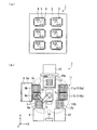
図1(a)は半導体基板を示す模式平面図である。図1(a)に示すように、基材としての半導体基板1は基板2を備えている。基板2は耐熱性があり半導体装置3を実装可能であれば良く、基板2にはガラスエポキシ基板、紙フェノール基板、紙エポキシ基板等を用いることができる。
(Semiconductor substrate)
First, a semiconductor substrate which is an example of an object to be drawn (printed) using a printing apparatus will be described.
FIG. 1A is a schematic plan view showing a semiconductor substrate. As shown in FIG. 1A, a
基板2上には半導体装置3が実装されている。そして、半導体装置3上には会社名マーク4、機種コード5、製造番号6等のマーク(印刷パターン、所定パターン)が描画されている。これらのマークが印刷装置によって描画される。
A semiconductor device 3 is mounted on the
(印刷装置)
図1(b)は印刷装置を示す模式平面図である。
図1(b)に示すように、印刷装置7は主に供給部8、前処理部9、塗布部(印刷部)10、冷却部11、収納部12、搬送部13及び制御部14から構成されている。印刷装置7は搬送部13を中心にして時計回りに供給部8、前処理部9、塗布部10、冷却部11、収納部12、制御部14の順に配置されている。そして、制御部14の隣には供給部8が配置されている。供給部8、制御部14、収納部12が並ぶ方向をX方向とする。X方向と直交する方向をY方向とし、Y方向には塗布部10、搬送部13、制御部14が並んで配置されている。そして、鉛直方向をZ方向とする。
(Printer)
FIG. 1B is a schematic plan view showing the printing apparatus.
As shown in FIG. 1B, the
供給部8は、複数の半導体基板1が収納された収納容器を備えている。そして、供給部8は中継場所8aを備え、収納容器から中継場所8aへ半導体基板1を供給する。
The
前処理部9は、半導体装置3の表面を加熱しながら改質する機能を有する。前処理部9により半導体装置3は吐出された液滴の広がり具合及び印刷するマークの密着性が調整される。前処理部9は第1中継場所9a及び第2中継場所9bを備え、処理前の半導体基板1を第1中継場所9aまたは第2中継場所9bから取り込んで表面の改質を行う。その後、前処理部9は処理後の半導体基板1を第1中継場所9aまたは第2中継場所9bに移動して、半導体基板1を待機させる。第1中継場所9a及び第2中継場所9bを合わせて中継場所9cとする。そして、前処理部9の内部で前処理が行われる場所を処理場所9dとする。
The
冷却部11は、前処理部9で加熱及び表面改質が行われた半導体基板1を冷却する機能を有している。冷却部11は、それぞれが半導体基板1を保持して冷却する処理場所11a、11bを有している。処理場所11a、11bは、適宜、処理場所11cと総称するものとする。
The cooling
塗布部10は、半導体装置3に液滴を吐出してマークを描画(印刷)するとともに、描画されたマークを固化または硬化する機能を有する。塗布部10は中継場所10aを備え、描画前の半導体基板1を中継場所10aから移動して描画処理及び硬化処理を行う。その後、塗布部10は描画後の半導体基板1を中継場所10aに移動して、半導体基板1を待機させる。
The
収納部12は、半導体基板1を複数収納可能な収納容器を備えている。そして、収納部12は中継場所12aを備え、中継場所12aから収納容器へ半導体基板1を収納する。操作者は半導体基板1が収納された収納容器を印刷装置7から搬出する。
The
印刷装置7の中央の場所には、搬送部13が配置されている。搬送部13は2つの腕部を備えたスカラー型ロボットが用いられている。そして、腕部の先端には半導体基板1を把持する把持部13aが設置されている。中継場所8a,9c,10a,11c,12aは把持部13aの移動範囲13b内に位置している。従って、把持部13aは中継場所8a,9c,10a,11c,12a間で半導体基板1を移動することができる。制御部14は印刷装置7の全体の動作を制御する装置であり、印刷装置7の各部の動作状況を管理する。そして、搬送部13に半導体基板1を移動する指示信号を出力する。これにより、半導体基板1は各部を順次通過して描画されるようになっている。
A
以下、各部の詳細について説明する。
(供給部)
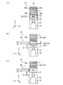
図2(a)は供給部を示す模式正面図であり、図2(b)及び図2(c)は供給部を示す模式側面図である。図2(a)及び図2(b)に示すように、供給部8は基台15を備えている。基台15の内部には昇降装置16が設置されている。昇降装置16はZ方向に動作する直動機構を備えている。この直動機構はボールネジと回転モーターとの組合せや油圧シリンダーとオイルポンプの組合せ等の機構を用いることができる。本実施形態では、例えば、ボールネジとステップモーターとによる機構を採用している。基台15の上側には昇降板17が昇降装置16と接続して設置されている。そして、昇降板17は昇降装置16により所定の移動量だけ昇降可能になっている。
Details of each part will be described below.
(Supply section)
FIG. 2A is a schematic front view showing the supply unit, and FIGS. 2B and 2C are schematic side views showing the supply unit. As shown in FIGS. 2A and 2B, the
昇降板17の上には直方体状の収納容器18が設置され、収納容器18の中には複数の半導体基板1が収納されている。収納容器18はY方向の両面に開口部18aが形成され、開口部18aから半導体基板1が出し入れ可能となっている。収納容器18のX方向の両側に位置する側面18bの内側には凸状のレール18cが形成され、レール18cはY方向に延在して配置されている。レール18cはZ方向に複数等間隔に配列されている。このレール18cに沿って半導体基板1をY方向からまたは−Y方向から挿入することにより、半導体基板1がZ方向に配列して収納される。
A rectangular
基台15のY方向側には支持部材21を介して、基板引出部22と中継台23とが設置されている。収納容器18のY方向側の場所において基板引出部22の上に中継台23が重ねて配置されている。基板引出部22はY方向に伸縮する腕部22aと腕部22aを駆動する直動機構とを備えている。この直動機構は直線状に移動する機構であれば特に限定されない、本実施形態では、例えば、圧縮空気にて作動するエアーシリンダーを採用している。腕部22aの一端には略矩形に折り曲げられた爪部22bが設置され、この爪部22bの先端は腕部22aと平行に形成されている。
On the Y direction side of the
基板引出部22が腕部22aを伸ばすことにより、腕部22aが収納容器18内を貫通する。そして、爪部22bが収納容器18の−Y方向側に移動する。次に昇降装置16が半導体基板1を下降した後、基板引出部22が腕部22aを収縮させる。このとき、爪部22bが半導体基板1の一端を押しながら移動する。
The substrate pull-out
その結果、図2(c)に示すように、半導体基板1が収納容器18から中継台23上に移動させられる。中継台23は半導体基板1のX方向の幅と略同じ幅の凹部が形成され、半導体基板1はこの凹部に沿って移動する。そして、この凹部により半導体基板1のX方向の位置が決められる。爪部22bによって押されて半導体基板1が停止する場所により、半導体基板1のY方向の位置が決められる。中継台23上は中継場所8aであり、半導体基板1は中継場所8aの所定の場所にて待機する。供給部8の中継場所8aに半導体基板1が待機しているとき、搬送部13は把持部13aを半導体基板1と対向する場所に移動して半導体基板1を把持して移動する。
As a result, as shown in FIG. 2C, the
この半導体基板1が搬送部13により中継台23上から移動した後、基板引出部22が腕部22aを伸長させる。次に、昇降装置16が収納容器18を降下させて、基板引出部22が半導体基板1を収納容器18内から中継台23上に移動させる。このようにして供給部8は順次半導体基板1を収納容器18から中継台23上に移動する。収納容器18内の半導体基板1を総て中継台23上に移動した後、操作者は空になった収納容器18と半導体基板1が収納されている収納容器18とを置き換える。これにより、供給部8に半導体基板1を供給することができる。
After the
(前処理部)
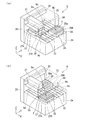
図3は前処理部の構成を示す概略斜視図である。図3(a)に示すように、前処理部9は基台24を備え、基台24上にはX方向に延在するそれぞれ一対の第1案内レール25及び第2案内レール26が並んで設置されている。第1案内レール25上には第1案内レール25に沿ってX方向に往復移動する載置台としての第1ステージ27が設置され、第2案内レール26上には第2案内レール26に沿ってX方向に往復移動する載置台としての第2ステージ28が設置されている。第1ステージ27及び第2ステージ28は直動機構を備え、往復移動することができる。この直動機構は、例えば、昇降装置16が備える直動機構と同様の機構を用いることができる。
(Pre-processing section)
FIG. 3 is a schematic perspective view showing the configuration of the preprocessing unit. As shown in FIG. 3A, the
第1ステージ27の上面には載置面27aが設置され、載置面27aには吸引式のチャック機構が形成されている。搬送部13が半導体基板1を載置面27aに載置した後、チャック機構を作動させることにより前処理部9は半導体基板1を載置面27aに固定することができる。同様に、第2ステージ28の上面にも載置面28aが設置され、載置面28aには吸引式のチャック機構が形成されている。搬送部13が半導体基板1を載置面28aに載置した後、チャック機構を作動させることにより前処理部9は半導体基板1を載置面28aに固定することができる。
A
第1ステージ27には、加熱装置27Hが内蔵されており、載置面27aに載置された半導体基板1を、制御部14の制御下で所定温度に加熱する。同様に、第2ステージ28には、加熱装置28Hが内蔵されており、載置面28aに載置された半導体基板1を、制御部14の制御下で所定温度に加熱する。
The
第1ステージ27がX方向側に位置するときの載置面27aの場所が第1中継場所9aとなっており、第2ステージ28がX方向に位置するときの載置面28aの場所が第2中継場所9bとなっている。第1中継場所9a及び第2中継場所9bである中継場所9cは把持部13aの動作範囲内に位置しており、中継場所9cにおいて載置面27a及び載置面28aは露出する。従って、搬送部13は容易に半導体基板1を載置面27a及び載置面28aに載置することができる。半導体基板1に前処理が行われた後、半導体基板1は第1中継場所9aに位置する載置面27aまたは第2中継場所9bに位置する載置面28a上にて待機する。従って、搬送部13の把持部13aは容易に半導体基板1を把持して移動することができる。
The place of the
基台24の−X方向には平板状の支持部29が立設されている。支持部29のX方向側の面において上側にはY方向に延在する案内レール30が設置されている。そして、案内レール30と対向する場所には案内レール30に沿って移動するキャリッジ31が設置されている。キャリッジ31は直動機構を備え、往復移動することができる。この直動機構は、例えば、昇降装置16が備える直動機構と同様の機構を用いることができる。
A flat plate-
キャリッジ31の基台24側には処理部32が設置されている。処理部32としては、例えば、活性光線を発光する低圧水銀ランプ、水素バーナー、エキシマレーザー、プラズマ放電部、コロナ放電部等を例示できる。水銀ランプを用いる場合、半導体基板1に紫外線を照射することにより、半導体基板1の表面の撥液性を改質することができる。水素バーナーを用いる場合、半導体基板1の酸化した表面を一部還元することで表面を粗面化することができ、エキシマレーザーを用いる場合、半導体基板1の表面を一部溶融固化することで粗面化することができ、プラズマ放電或いはコロナ放電を用いる場合、半導体基板1の表面を機械的に削ることで粗面化することができる。本実施形態では、例えば、水銀ランプを採用している。前処理部9は、加熱装置27H、28Hにより半導体基板1を加熱した状態で、処理部32から紫外線を照射しながらキャリッジ31を往復運動させる。これにより、前処理部9は、処理場所9dの広い範囲に紫外線を照射することが可能になっている。
A
前処理部9は、外装部33により全体が覆われている。外装部33の内部には上下に移動可能な戸部34が設置されている。そして、図3(b)に示すように、第1ステージ27または第2ステージ28がキャリッジ31と対向する場所に移動したあと、戸部34が下降する。これにより、処理部32が照射する紫外線が前処理部9の外に漏れないようになっている。
The
載置面27aもしくは載置面28aが中継場所9cに位置するとき、搬送部13は載置面27a及び載置面28aに半導体基板1を給材する。そして、前処理部9は半導体基板1が載置された第1ステージ27もしくは第2ステージ28を処理場所9dに移動して前処理を行う。前処理が終了した後、前処理部9は第1ステージ27もしくは第2ステージ28を中継場所9cに移動する。続いて、搬送部13は載置面27aもしくは載置面28aから半導体基板1を除材する。
When the mounting
(冷却部)
冷却部11は、各処理場所11a、11bにそれぞれ設けられ、上面が半導体装置1の吸着保持面とされたヒートシンク等の冷却板110a、110bを有している。
処理場所11a、11b(冷却板110a、110b)は、把持部13aの動作範囲内に位置しており、処理場所11a、11bにおいて冷却板110a、110bは露出する。従って、搬送部13は容易に半導体基板1を冷却板110a、110bに載置することができる。半導体基板1に冷却処理が行われた後、半導体基板1は、処理場所11aに位置する冷却板110a上または処理場所11bに位置する冷却板110a上にて待機する。従って、搬送部13の把持部13aは容易に半導体基板1を把持して移動させることができる。
(Cooling section)
The cooling
The
(塗布部)
次に、半導体基板1に液滴を吐出してマークを形成する塗布部10について図4及び図5に従って説明する。液滴を吐出する装置に関しては様々な種類の装置があるが、インクジェット法を用いた装置が好ましい。インクジェット法は微小な液滴の吐出が可能であるため、微細加工に適している。
(Applying part)
Next, the
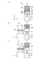
図4(a)は、塗布部の構成を示す概略斜視図である。塗布部10により半導体基板1に液滴が吐出される。図4(a)に示すように、塗布部10には、直方体形状に形成された基台37を備えている。液滴を吐出するときに液滴吐出ヘッドと被吐出物とが相対移動する方向を主走査方向とする。そして、主走査方向と直交する方向を副走査方向とする。副走査方向は改行するときに液滴吐出ヘッドと被吐出物とを相対移動する方向である。本実施形態ではX方向を主走査方向とし、Y方向を副走査方向とする。
FIG. 4A is a schematic perspective view showing the configuration of the application unit. Liquid droplets are ejected onto the
基台37の上面37aには、Y方向に延在する一対の案内レール38がY方向全幅にわたり凸設されている。その基台37の上側には、一対の案内レール38に対応する図示しない直動機構を備えたステージ39が取付けられている。そのステージ39の直動機構は、リニアモーターやネジ式直動機構等を用いることができる。本実施形態では、例えば、リニアモーターを採用している。そして、Y方向に沿って所定の速度で往動または復動するようになっている。往動と復動を繰り返すことを走査移動と称す。さらに、基台37の上面37aには、案内レール38と平行に副走査位置検出装置40が配置され、副走査位置検出装置40によりステージ39の位置が検出される。
On the
そのステージ39の上面には載置面41が形成され、その載置面41には図示しない吸引式の基板チャック機構が設けられている。載置面41上に半導体基板1が載置された後、半導体基板1は基板チャック機構により載置面41に固定される。
A
ステージ39が−Y方向に位置するときの載置面41の場所が中継場所10aとなっている。この載置面41は把持部13aの動作範囲内に露出するように設置されている。従って、搬送部13は容易に半導体基板1を載置面41に載置することができる。半導体基板1に塗布が行われた後、半導体基板1は中継場所10aである載置面41上にて待機する。従って、搬送部13の把持部13aは容易に半導体基板1を把持して移動することができる。
The place of the
基台37のX方向両側には一対の支持台42が立設され、その一対の支持台42にはX方向に延びる案内部材43が架設されている。案内部材43の下側にはX方向に延びる案内レール44がX方向全幅にわたり凸設されている。案内レール44に沿って移動可能に取り付けられるキャリッジ(移動手段)45は略直方体形状に形成されている。そのキャリッジ45は直動機構を備え、その直動機構は、例えば、ステージ39が備える直動機構と同様の機構を用いることができる。そして、キャリッジ45がX方向に沿って走査移動する。案内部材43とキャリッジ45との間には主走査位置検出装置46が配置され、キャリッジ45の位置が計測される。キャリッジ45の下側にはヘッドユニット47が設置され、ヘッドユニット47のステージ39側の面には図示しない液滴吐出ヘッドが凸設されている。
A pair of
図4(b)は、キャリッジを示す模式側面図である。図4(b)に示すようにキャリッジ45の半導体基板1側にはヘッドユニット47と一対の照射部としての硬化ユニット48が配置されている。ヘッドユニット47の半導体基板1側には液滴を吐出する液滴吐出ヘッド(吐出ヘッド)49が凸設されている。
FIG. 4B is a schematic side view showing the carriage. As shown in FIG. 4B, a
硬化ユニット48の内部には吐出された液滴を硬化させる紫外線を照射する照射装置が配置されている。硬化ユニット48は主走査方向(相対移動方向)においてヘッドユニット47を挟んだ両側の位置に配置されている。照射装置は発光ユニットと放熱板等から構成されている。発光ユニットには多数のLED(Light Emitting Diode)素子が配列して設置されている。このLED素子は、電力の供給を受けて紫外線の光である紫外光を発光する素子である。
An irradiating device for irradiating ultraviolet rays that cure the discharged droplets is disposed inside the curing
キャリッジ45の図中上側には収容タンク50が配置され、収容タンク50には機能液が収容されている。液滴吐出ヘッド49と収容タンク50とは図示しないチューブにより接続され、収容タンク50内の機能液がチューブを介して液滴吐出ヘッド49に供給される。
A
機能液は樹脂材料、硬化剤としての光重合開始剤、溶媒または分散媒を主材料とする。この主材料に顔料または染料等の色素や、親液性または撥液性等の表面改質材料等の機能性材料を添加することにより固有の機能を有する機能液を形成することができる。本実施形態では、例えば、白色の顔料を添加している。機能液の樹脂材料は樹脂膜を形成する材料である。樹脂材料としては、常温で液状であり、重合させることによりポリマーとなる材料であれば特に限定されない。さらに、粘性の小さい樹脂材料が好ましく、オリゴマーの形態であるのが好ましい。モノマーの形態であればさらに好ましい。光重合開始剤はポリマーの架橋性基に作用して架橋反応を進行させる添加剤であり、例えば、光重合開始剤としてベンジルジメチルケタール等を用いることができる。溶媒または分散媒は樹脂材料の粘度を調整するものである。機能液を液滴吐出ヘッドから吐出し易い粘度にすることにより、液滴吐出ヘッドは安定して機能液を吐出することができるようになる。 The functional liquid is mainly composed of a resin material, a photopolymerization initiator as a curing agent, a solvent or a dispersion medium. A functional liquid having an inherent function can be formed by adding a coloring material such as a pigment or a dye or a functional material such as a lyophilic or liquid repellent surface modifying material to the main material. In this embodiment, for example, a white pigment is added. The functional liquid resin material is a material for forming a resin film. The resin material is not particularly limited as long as the material is liquid at normal temperature and becomes a polymer by polymerization. Furthermore, a resin material having a low viscosity is preferable, and it is preferably in the form of an oligomer. A monomer form is more preferable. The photopolymerization initiator is an additive that acts on a crosslinkable group of the polymer to advance the crosslinking reaction. For example, benzyldimethyl ketal or the like can be used as the photopolymerization initiator. The solvent or the dispersion medium adjusts the viscosity of the resin material. By setting the viscosity at which the functional liquid can be easily discharged from the droplet discharge head, the droplet discharge head can stably discharge the functional liquid.
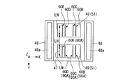
図5(a)は、ヘッドユニットを示す模式平面図である。図5(a)に示すように、ヘッドユニット47には第1、第2の吐出ヘッドを構成する2つの液滴吐出ヘッド49が副走査方向に間隔をあけて配置され、各液滴吐出ヘッド49の表面にはノズルプレート51がそれぞれ配置されている。各ノズルプレート51には複数のノズル52が配列して形成されている。本実施形態においては、各ノズルプレート51に、15個のノズル52が副走査方向に沿って配置されたノズル列60が一列設けられている。また、2つのノズル列60は、Y方向に沿った直線状に、且つX方向については両側の硬化ユニット48と等間隔となる位置に配置されている。
FIG. 5A is a schematic plan view showing the head unit. As shown in FIG. 5A, in the
各液滴吐出ヘッド49においては、ノズル列60の両端に位置するノズル52については液滴の吐出特性が不安定になる傾向があるため、液滴吐出処理には用いない。すなわち、本実施形態では、両端のノズル52を除く13個のノズル52によって、実際に半導体基板1に対して液滴を吐出する実ノズル列60Aが形成される。
In each
ここで、各実ノズル列60Aの副走査方向の長さをLNとし、隣り合う液滴吐出ヘッド49同士の実ノズル列60A間の副走査方向の距離をLHとすると、隣り合う液滴吐出ヘッド49は、以下の式を満足する位置関係で配置される。
LH=n×LN(nは正の整数) …(1)
本実施形態では、n=1、すなわち、LH=LNとなる位置関係で二つの液滴吐出ヘッド49がY方向に沿って配置されている。
Here, when the length of each
LH = n × LN (n is a positive integer) (1)
In the present embodiment, two droplet discharge heads 49 are arranged along the Y direction with a positional relationship of n = 1, that is, LH = LN.
硬化ユニット48の下面には、照射口48aが形成されている。照射口48aは、Y方向における吐出ヘッド49、49の長さ、これら吐出ヘッド49、49間の距離の和以上の長さの照射範囲を有して設けられている。そして、照射装置が発光する紫外光が照射口48aから半導体基板1に向けて照射される。
An
図5(b)は、液滴吐出ヘッドの構造を説明するための要部模式断面図である。図5(b)に示すように、液滴吐出ヘッド49はノズルプレート51を備え、ノズルプレート51にはノズル52が形成されている。ノズルプレート51の上側であってノズル52と相対する位置にはノズル52と連通するキャビティ53が形成されている。そして、液滴吐出ヘッド49のキャビティ53には機能液(液体)54が供給される。
FIG. 5B is a schematic cross-sectional view of a main part for explaining the structure of the droplet discharge head. As shown in FIG. 5B, the
キャビティ53の上側には上下方向に振動してキャビティ53内の容積を拡大縮小する振動板55が設置されている。振動板55の上側でキャビティ53と対向する場所には上下方向に伸縮して振動板55を振動させる圧電素子56が配設されている。圧電素子56が上下方向に伸縮して振動板55を加圧して振動し、振動板55がキャビティ53内の容積を拡大縮小してキャビティ53を加圧する。それにより、キャビティ53内の圧力が変動し、キャビティ53内に供給された機能液54はノズル52を通って吐出される。
A
液滴吐出ヘッド49が圧電素子56を制御駆動するためのノズル駆動信号を受けると、圧電素子56が伸張して、振動板55がキャビティ53内の容積を縮小する。その結果、液滴吐出ヘッド49のノズル52から縮小した容積分の機能液54が液滴57となって吐出される。機能液54が塗布された半導体基板1に対しては、照射口48aから紫外光が照射され、硬化剤を含んだ機能液54を固化または硬化させるようになっている。
When the
(収納部)
図6(a)は収納部を示す模式正面図であり、図6(b)及び図6(c)は収納部を示す模式側面図である。図6(a)及び図6(b)に示すように、収納部12は基台74を備えている。基台74の内部には昇降装置75が設置されている。昇降装置75は供給部8に設置された昇降装置16と同様の装置を用いることができる。基台74の上側には昇降板76が昇降装置75と接続して設置されている。そして、昇降板76は昇降装置75により昇降させられる。昇降板76の上には直方体状の収納容器18が設置され、収納容器18の中には半導体基板1が収納されている。収納容器18は供給部8に設置された収納容器18と同じ容器が用いられている。
(Storage section)
FIG. 6A is a schematic front view showing the storage portion, and FIGS. 6B and 6C are schematic side views showing the storage portion. As shown in FIGS. 6A and 6B, the
基台74のY方向側には支持部材77を介して、基板押出部78と中継台79とが設置されている。収納容器18のY方向側の場所において基板押出部78の上に中継台79が重ねて配置されている。基板押出部78はY方向に移動する腕部78aと腕部78aを駆動する直動機構とを備えている。この直動機構は直線状に移動する機構であれば特に限定されない、本実施形態では、例えば、圧縮空気にて作動するエアーシリンダーを採用している。中継台79上には半導体基板1が載置され、この半導体基板1のY方向側の一端の中央に腕部78aが接触可能となっている。
A
基板押出部78が腕部78aを−Y方向に移動させることにより、腕部78aが半導体基板1を−Y方向に移動させる。中継台79は半導体基板1のX方向の幅と略同じ幅の凹部が形成され、半導体基板1はこの凹部に沿って移動する。そして、この凹部により半導体基板1のX方向の位置が決められる。その結果、図6(c)に示すように、半導体基板1が収納容器18の中に移動させられる。収納容器18にはレール18cが形成されており、レール18cは中継台79に形成された凹部の延長線上に位置するようになっている。そして、基板押出部78によって半導体基板1はレール18cに沿って移動させられる。これにより、半導体基板1は収納容器18に品質良く収納される。
The
搬送部13が中継台79上に半導体基板1を移動した後、昇降装置75が収納容器18を上昇させる。そして、基板押出部78が腕部78aを駆動して半導体基板1を収納容器18内に移動させる。このようにして収納部12は半導体基板1を収納容器18内に収納する。収納容器18内に所定の枚数の半導体基板1が収納された後、操作者は半導体基板1が収納された収納容器18と空の収納容器18とを置き換える。これにより、操作者は複数の半導体基板1をまとめて次の工程に持ち運ぶことができる。
After the
収納部12は収納する半導体基板1を載置する中継場所12aを有している。搬送部13は半導体基板1を中継場所12aに載置するだけで、収納部12と連携して半導体基板1を収納容器18に収納することができる。
The
(搬送部)
次に、半導体基板1を搬送する搬送部13について図7に従って説明する。図7は、搬送部の構成を示す概略斜視図である。図7に示すように、搬送部13は平板状に形成された基台82を備えている。基台82上には支持台83が配置されている。支持台83の内部には空洞が形成され、この空洞にはモーター、角度検出器、減速機等から構成される回転機構83aが設置されている。そして、モーターの出力軸は減速機と接続され、減速機の出力軸は支持台83の上側に配置された第1腕部84と接続されている。また、モーターの出力軸と連結して角度検出器が設置され、角度検出器がモーターの出力軸の回転角度を検出する。これにより、回転機構83aは第1腕部84の回転角度を検出して、所望の角度まで回転させることができる。
(Transport section)
Next, the
第1腕部84上において支持台83と反対側の端には回転機構85が設置されている。回転機構85はモーター、角度検出器、減速機等により構成され、支持台83の内部に設置された回転機構と同様の機能を備えている。そして、回転機構85の出力軸は第2腕部86と接続されている。これにより、回転機構85は第2腕部86の回転角度を検出して、所望の角度まで回転させることができる。
A
第2腕部86上において回転機構85と反対側の端には昇降装置87が配置されている。昇降装置87は直動機構を備え、直動機構を駆動することにより伸縮することができる。この直動機構は、例えば、供給部8の昇降装置16と同様の機構を用いることができる。昇降装置87の下側には回転装置88が配置されている。
On the
回転装置88は回転角度を制御可能であれば良く、各種モーターと回転角度センサーとを組み合わせて構成することができる。他にも、回転角度を所定の角度にて回転できるステップモーターを用いることができる。本実施形態では、例えば、ステップモーターを採用している。さらに減速装置を配置しても良い。さらに細かな角度で回転させることができる。
The
回転装置88の図中下側には把持部13aが配置されている。そして、把持部13aは回転装置88の回転軸と接続されている。従って、搬送部13は回転装置88を駆動することにより把持部13aを回転させることができる。さらに、搬送部13は昇降装置87を駆動することにより把持部13aを昇降させることができる。
A gripping
把持部13aは4本の直線状の指部13cを有し、指部13cの先端には半導体基板1を吸引して吸着させる吸着機構が形成されている。そして、把持部13aはこの吸着機構を作動させて、半導体基板1を把持することができる。
The gripping
基台82の−Y方向側には制御装置89が設置されている。制御装置89には中央演算装置、記憶部、インターフェース、アクチュエーター駆動回路、入力装置、表示装置等を備えている。アクチュエーター駆動回路は回転機構83a、回転機構85、昇降装置87、回転装置88、把持部13aの吸着機構を駆動する回路である。そして、これらの装置及び回路はインターフェースを介して中央演算装置と接続されている。他にも角度検出器がインターフェースを介して中央演算装置と接続されている。記憶部には搬送部13を制御する動作手順を示したプログラムソフトや制御に用いるデータが記憶されている。中央演算装置はプログラムソフトに従って搬送部13を制御する装置である。制御装置89は搬送部13に配置された検出器の出力を入力して把持部13aの位置と姿勢とを検出する。そして、制御装置89は回転機構83a及び回転機構85を駆動して把持部13aを所定の位置に移動させる制御を行う。
A
(印刷方法)
次に上述した印刷装置7を用いた印刷方法について図8にて説明する。図8は、印刷方法を示すためのフローチャートである。
図8のフローチャートに示されるように、印刷方法は、半導体基板1を収納容器18から搬入する搬入工程S1、搬入された半導体基板1の表面に対して前処理を施す前処理工程(第1工程)S2、前処理工程S2で温度上昇した半導体基板1を冷却する冷却工程(第2工程)S3、冷却された半導体基板1に対して各種マークを描画印刷する印刷工程(第3工程)S4、各種マークが印刷された半導体基板1を収納容器18に収納する収納工程S5を主体に構成される。
(Printing method)
Next, a printing method using the above-described
As shown in the flowchart of FIG. 8, the printing method includes a carry-in step S <b> 1 for carrying in the
上記の工程の中、前処理工程S2から印刷工程S4に至る工程が本発明の特徴部分であるため、以下の説明においては、この特徴部分について説明する。
前処理工程S2においては、前処理部9では第1ステージ27と第2ステージ28とのうち一方のステージが中継場所9cに位置している。搬送部13は中継場所9cに位置するステージと対向する場所に把持部13aを移動させる。続いて、搬送部13は把持部13aを下降させた後、半導体基板1の吸着を解除することにより、半導体基板1を中継場所9cに位置する第1ステージ27もしくは第2ステージ28上に載置する。その結果、図9(b)に示すように、中継場所9cに位置する第1ステージ27上に半導体基板1が載置される。もしくは、図9(c)に示すように、中継場所9cに位置する第2ステージ28上に半導体基板1が載置される。
Among the steps described above, the steps from the pretreatment step S2 to the printing step S4 are the characteristic portions of the present invention. Therefore, the characteristic portions will be described in the following description.
In the preprocessing step S2, in the
第1ステージ27及び第2ステージ28は、加熱装置27H、28Hにより予め加熱されており、第1ステージ27または第2ステージ28に載置された半導体基板1は直ちに所定温度に加熱される。半導体基板1を加熱する温度としては、後述するように、半導体基板1の表面を効果的に改質あるいは表面の有機物除去を効率的に行え、且つ半導体基板1の耐熱温度以下であることが好ましく、本実施形態では、半導体基板1を150℃〜200℃の範囲の温度となるように、例えば180℃の温度に加熱している。
The
また、搬送部13が第1ステージ27上に半導体基板1を移動するとき、前処理部9の内部にある処理場所9dでは第2ステージ28上の半導体基板1の前処理が行われている。そして、第2ステージ28上の半導体基板1の前処理が終了した後、第2ステージ28が第2中継場所9bに半導体基板1を移動させる。次に、前処理部9は第1ステージ27を駆動することにより、第1中継場所9aに載置された半導体基板1をキャリッジ31と対向する処理場所9dに移動させる。これにより、第2ステージ28上の半導体基板1の前処理が終了した後、すぐに、第1ステージ27上の半導体基板1の前処理を開始することができる。
Further, when the
続いて、前処理部9では、半導体基板1に実装された半導体装置3に紫外線を照射する。これにより、半導体装置3の表面層における有機系被照射物の化学結合を切断するとともに、紫外線で発生したオゾンから分離した活性酸素がその切断された表面層の分子に結合し、親水性の高い官能基(例えば-OH、-CHO、-COOH)に変換され、基板1の表面を改質するとともに、表面の有機物除去が行われる。ここで、半導体装置3(半導体基板1)は、上述したように、予め180℃に加熱された状態で紫外線が照射されるため、半導体基板1に損傷が及ぶことなく、表面層の分子の衝突速度を大きくして、効果的に表面を改質できるとともに、表面の有機物を効率的に除去できる。前処理を行った後に前処理部9は第1ステージ27を駆動することにより、半導体基板1を第1中継場所9aに移動させる。
Subsequently, in the
同様に、搬送部13が第2ステージ28上に半導体基板1を移動するときには、前処理部9の内部にある処理場所9dでは第1ステージ27上の半導体基板1の前処理が行われている。そして、第1ステージ27上の半導体基板1の前処理が終了した後、第1ステージ27が第1中継場所9aに半導体基板1を移動させる。次に、前処理部9は第2ステージ28を駆動することにより、第2中継場所9bに載置された半導体基板1をキャリッジ31と対向する処理場所9dに移動させる。これにより、第1ステージ27上の半導体基板1の前処理が終了した後、直に、第2ステージ28上の半導体基板1の前処理を開始することができる。続いて、前処理部9は半導体基板1に実装された半導体装置3に紫外線を照射することにより、上記第1ステージ27上の半導体基板1と同様に、半導体基板1に損傷が及ぶことなく、効果的に表面を改質できるとともに、表面の有機物を効率的に除去できる。前処理を行った後に前処理部9は第2ステージ28を駆動することにより、半導体基板1を第2中継場所9bに移動させる。
Similarly, when the
前処理工程S2で半導体基板1の前処理が完了し、冷却工程S3に移行すると、搬送部13は中継場所9cにある半導体基板1を処理場所11a、11bに設けられた冷却板110aまたは110bに載置する。これにより、前処理工程S2で加熱された半導体基板1は、印刷工程S4が行われる際の適切な温度(例えば室温)に所定時間冷却(温度調整)される。
When the pretreatment of the
冷却工程S3で冷却された半導体基板1は、搬送部13により塗布部10の中継場所10aに位置するステージ39上に搬送される。印刷工程S5において、塗布部10はチャック機構を作動させてステージ39上に載置された半導体基板1をステージ39に保持する。そして、塗布部10は、ステージ39に対してキャリッジ45を、例えば+X方向に走査移動(相対移動)しながら、各液滴吐出ヘッド49に形成されたノズル52から液滴57を吐出する。
The
これにより、半導体装置3の表面には会社名マーク4、機種コード5、製造番号6等のマークが描画される。そして、走査移動方向における後方側であるキャリッジ45の−X側に設置された硬化ユニット48からマークに紫外線が照射される。これにより、マークを形成する機能液54には紫外線により重合が開始する光重合開始剤が含まれているため、マークの表面が直ちに固化または硬化される。
Thereby, marks such as the company name mark 4, the
このとき、二つの液滴吐出ヘッド49は、副走査方向であるY方向に沿って配置され、ノズル列60についてもY方向に直線状に配置されているため、液滴57が半導体装置3に吐出されてから紫外線に照射されて硬化するまでのピニング時間は、二つの液滴吐出ヘッド49間で差が生じずに同一となる。
At this time, the two droplet discharge heads 49 are arranged along the Y direction which is the sub-scanning direction, and the
キャリッジ45の+X方向への走査移動が完了すると、ステージ39を例えば+Y方向に距離LN(=LH)フィードする。そして、ステージ39に対してキャリッジ45を、−X方向に走査移動(相対移動)しながら、各液滴吐出ヘッド49に形成されたノズル52から液滴57を吐出しつつ、走査移動方向における後方側であるキャリッジ45の+X側に設置された硬化ユニット48からマークに紫外線が照射される。
When the scanning movement of the
これにより、一回目の走査移動で液滴が吐出されなかった二つの液滴吐出ヘッド49間のエリアに対しても液滴が吐出される。また、二回目の走査移動による液滴吐出においても、液滴57が半導体装置3に吐出されてから紫外線に照射されて硬化するまでのピニング時間は、二つの液滴吐出ヘッド49間で差が生じずに同一となる。さらに、ノズル列60(実ノズル列60A)と両側の硬化ユニット48とのX方向の距離が同一であるため、一回目の走査移動による液滴吐出と二回目の走査移動による液滴吐出とでピニング時間が同一となる。
As a result, droplets are also ejected to the area between the two droplet ejection heads 49 where the droplets were not ejected by the first scanning movement. Also, in the droplet discharge by the second scanning movement, the pinning time from when the
半導体基板1に対する印刷を行った後に塗布部10は半導体基板1が載置されたステージ39を中継場所10aに移動させる。これにより、搬送部13が半導体基板1を把持し易くすることができる。そして、塗布部10はチャック機構の動作を停止して半導体基板1の保持を解除する。
After printing on the
この後、半導体基板1は、収納工程S5において、搬送部13により収納部12に搬送され、収納容器18に収納される。
Thereafter, the
以上説明したように、本実施形態では、二つの液滴吐出ヘッド49を副走査方向であるY方向に沿って配置しているため、各液滴吐出ヘッド49から吐出した液滴57のピニング時間を同一とすることができる。そのため、本実施形態では、形成されたマークの描画品質を一定とすることができ印刷品質を確保することが可能になる。
As described above, in the present embodiment, since the two droplet discharge heads 49 are arranged along the Y direction which is the sub-scanning direction, the pinning time of the
また、本実施形態では、隣り合う液滴吐出ヘッド49同士の実ノズル列60A間のY方向の距離LHが、実ノズル列60AのY方向の長さLNの正の整数倍となるように、二つの液滴吐出ヘッド49を配置しているため、複数回の走査移動で半導体基板1に液滴を吐出する場合でも、最小回数の走査移動で液滴吐出処理を完了させることができ、生産性の向上に寄与できる。
Further, in the present embodiment, the distance LH in the Y direction between the
(第2実施形態)
続いて、印刷装置7の第2実施形態について、図9を参照して説明する。
この図において、図1乃至図8に示す第1実施形態の構成要素と同一の要素については同一符号を付し、その説明を省略する。
(Second Embodiment)
Next, a second embodiment of the
In this figure, the same components as those of the first embodiment shown in FIGS. 1 to 8 are denoted by the same reference numerals, and the description thereof is omitted.
図9に示すように、本実施形態における各液滴吐出ヘッド49には、Y方向に延びる複数のノズル列60B〜60EがX方向に間隔をあけて設けられている。両液滴吐出ヘッド49同士の各ノズル列60B〜60Eは、同一直線状に位置している。また、本実施形態でも、隣り合う液滴吐出ヘッド49同士の実ノズル列60A間のY方向の距離LHが、実ノズル列60AのY方向の長さLNの正の整数倍(ここでは1倍;LH=LN)となるように、二つの液滴吐出ヘッド49が配置されている。
他の構成は、上記第1実施形態と同様である。
As shown in FIG. 9, each
Other configurations are the same as those of the first embodiment.
上記構成の印刷装置7では、半導体基板1に対して液滴57を吐出する際に用いるノズル列は、制御部14によって同列のノズル列が選択される。例えば、いずれの液滴吐出ヘッド49についても、ノズル列60Bのみを用いて液滴吐出処理を行う。これにより、上記第1実施形態と同様の作用・効果を得ることができる。
In the
また、何らかの理由で、第1走査移動終了後に、第2走査移動時に第1走査移動時とは異なるノズル列を用いる場合、例えば第1走査移動でノズル列60Bのみを用いて液滴吐出処理を行い、第2走査移動でノズル列60Cを用いて液滴吐出処理を行う場合、+X方向の移動に関しては、走査移動方向の後方側に位置する硬化ユニット48までの距離が異なるため、ピニング時間が一定ではなくなる可能性がある。そのため、制御部14は、ノズル列と硬化ユニット48とのX方向の距離に応じて、走査移動速度を調整することによりピニング時間を一定とする。
For some reason, when a nozzle row different from the first scan movement is used during the second scan movement after the first scan movement, for example, the droplet discharge process is performed using only the
例えば、ノズル列60B、60Cと硬化ユニット48とのX方向の距離をそれぞれLB、LCとし、ノズル列60B、60Cを用いた場合の走査移動速度をそれぞれVB、VCとすると、制御部14は第1走査移動では速度VBの走査移動速度でノズル列60Bを用いて液滴吐出処理を行った後に、第2走査移動では速度VC=VB×(LC/LB)の走査移動速度でノズル列60Cを用いて液滴吐出処理を行わせる。
このように、走査移動速度を調整することにより、ピニング時間を一定とすることが可能になる。
For example, assuming that the distances in the X direction between the
Thus, the pinning time can be made constant by adjusting the scanning movement speed.
また、+X側への走査移動と−X側への走査移動との双方を行う場合には、走査移動方向に応じて、使用するノズル列を選択したり、同じノズル列を用いる場合には上述したように、走査移動速度を調整する構成とすることができる。
例えば、+X方向への走査移動時にノズル列60Bを用いて液滴吐出処理及び紫外線照射処理を行った場合には、−X方向への走査移動時にはノズル列60Dを用いて液滴吐出処理及び紫外線照射処理を行うことにより、各走査移動での移動速度が同一の場合には、両走査移動でのピニング時間を一定とすることが可能になる。
Further, when both the scanning movement to the + X side and the scanning movement to the −X side are performed, the nozzle row to be used is selected according to the scanning movement direction, or the same nozzle row is used as described above. As described above, the scanning movement speed can be adjusted.
For example, when the droplet ejection process and the ultraviolet irradiation process are performed using the
また、例えば、両走査移動時にノズル列60Bを用いる場合、+X側への走査移動時のノズル列60Bと走査移動方向後方側(−X側)の硬化ユニット48とのX方向の距離をLX1、−X側への走査移動時のノズル列60Bと走査移動方向後方側(+X側)の硬化ユニット48とのX方向の距離をLX2、+X側への走査速度をVX1、−X側への走査速度をVX2とすると、制御部14は+X側への走査移動では速度VX1の走査移動速度でノズル列60Bを用いて液滴吐出処理を行った後に、−X側への走査移動では、速度VX2=VX1×(LX2/LX1)の走査移動速度でノズル列60Bを用いて液滴吐出処理を行わせる。
このように、走査移動速度を調整することにより、ピニング時間を一定とすることが可能になる。
For example, when the
Thus, the pinning time can be made constant by adjusting the scanning movement speed.
以上、添付図面を参照しながら本発明に係る好適な実施形態について説明したが、本発明は係る例に限定されないことは言うまでもない。上述した例において示した各構成部材の諸形状や組み合わせ等は一例であって、本発明の主旨から逸脱しない範囲において設計要求等に基づき種々変更可能である。 As described above, the preferred embodiments according to the present invention have been described with reference to the accompanying drawings, but the present invention is not limited to the examples. Various shapes, combinations, and the like of the constituent members shown in the above-described examples are examples, and various modifications can be made based on design requirements and the like without departing from the gist of the present invention.
例えば、上記実施形態では、UVインクとして紫外線硬化型インクを用いたが、本発明はこれに限定されず、可視光線、赤外線を硬化光として使用することができる種々の活性光線硬化型インクを用いることができる。
また、光源も同様に、可視光等の活性光を射出する種々の活性光光源を用いること、つまり活性光線照射部を用いることができる。
For example, in the above embodiment, an ultraviolet curable ink is used as the UV ink, but the present invention is not limited to this, and various actinic ray curable inks that can use visible light and infrared light as curable light are used. be able to.
Similarly, various active light sources that emit active light such as visible light can be used as the light source, that is, an active light irradiation unit can be used.
ここで、本発明において「活性光線」とは、その照射によりインク中において開始種を発生させうるエネルギーを付与することができるものであれば、特に制限はなく、広く、α線、γ線、X線、紫外線、可視光線、電子線などを包含するものである。中でも、硬化感度及び装置の入手容易性の観点からは、紫外線及び電子線が好ましく、特に紫外線が好ましい。従って、活性光線硬化型インクとしては、本実施形態のように、紫外線を照射することにより硬化可能な紫外線硬化型インクを用いることが好ましい。 Here, in the present invention, the “actinic ray” is not particularly limited as long as it can impart energy capable of generating a starting species in the ink by the irradiation, and is broadly divided into α rays, γ rays, X-rays, ultraviolet rays, visible rays, electron beams and the like are included. Among these, from the viewpoints of curing sensitivity and device availability, ultraviolet rays and electron beams are preferable, and ultraviolet rays are particularly preferable. Therefore, as the actinic ray curable ink, it is preferable to use an ultraviolet curable ink that can be cured by irradiating ultraviolet rays as in the present embodiment.
上記実施形態では、ノズル列が副走査方向(Y方向)に延在する構成を例示したが、これに限られるものではなく、副走査方向と交差する方向(Y方向に対して所定角度傾く方向)に延在する構成であってもよい。
この場合、ノズル列を構成するノズルと硬化ユニット48との距離が一定ではなくなるため、例えばノズルと硬化ユニット48との距離の平均値を用いて、上記の調整すべき走査移動速度を求める構成としてもよい。
In the above embodiment, the configuration in which the nozzle row extends in the sub-scanning direction (Y direction) is exemplified, but the present invention is not limited to this, and the direction intersecting the sub-scanning direction (the direction inclined at a predetermined angle with respect to the Y direction). ) May be extended.
In this case, since the distance between the nozzles constituting the nozzle row and the curing
また、図9に示した第2実施形態のように、一つのノズルプレートが複数のノズル列を有する構成を採ることが好ましい。
これによれば、隣り合うノズル列を高密度で配置できるため、キャリッジ自体を小さくできる。また、ノズル列間距離と光源・複数のノズル列間距離との比を小さくできる。これにより、全ノズル列における平均的な、着弾から硬化までの時間をより短くできる。よって、着弾から硬化までの時間を一定に制御することが容易である。
Further, it is preferable to adopt a configuration in which one nozzle plate has a plurality of nozzle rows as in the second embodiment shown in FIG.
According to this, since the adjacent nozzle rows can be arranged with high density, the carriage itself can be made small. Further, the ratio between the distance between the nozzle rows and the distance between the light source and the plurality of nozzle rows can be reduced. Thereby, the average time from landing to curing in all nozzle rows can be further shortened. Therefore, it is easy to control the time from landing to curing to be constant.
1…半導体基板(基材)、 3…半導体装置、 7…印刷装置、 9…前処理部、 10…塗布部(印刷部)、 14…制御部、 45…キャリッジ(移動手段)、 48…硬化ユニット(照射部)、 49…液滴吐出ヘッド(吐出ヘッド)、 52…ノズル、 54…機能液(液体)、 57…液滴
DESCRIPTION OF
Claims (9)
前記吐出ヘッドは、前記相対移動方向と直交する方向に沿って複数設けられることを特徴とする印刷装置。 A discharge head that discharges a liquid droplet that moves relative to the substrate and is cured by actinic rays; and is disposed on the rear side in the relative movement direction with respect to the discharge head. An irradiation unit for irradiating the actinic ray,
A plurality of the ejection heads are provided along a direction orthogonal to the relative movement direction.
前記吐出ヘッドは、前記液滴を吐出する複数のノズルが前記相対移動方向と交差する方向に沿って配置されたノズル列を有し、
前記ノズル列のうち、前記基材に対して前記液滴を吐出するノズルで構成される実ノズル列の前記直交する方向の長さをLNとし、隣り合う前記吐出ヘッド同士の前記実ノズル列間の前記直交する方向の距離をLHとすると、
隣り合う前記吐出ヘッドは、LH=n×LN(nは正の整数)を満足する位置関係で配置されることを特徴とする印刷装置。 The printing apparatus according to claim 1.
The ejection head has a nozzle row in which a plurality of nozzles that eject the droplets are arranged along a direction intersecting the relative movement direction,
Among the nozzle rows, LN is the length in the orthogonal direction of the actual nozzle row composed of nozzles that discharge the droplets to the substrate, and the interval between the actual nozzle rows of the adjacent ejection heads is LN. If the distance in the orthogonal direction is LH,
The adjacent ejection heads are arranged in a positional relationship satisfying LH = n × LN (n is a positive integer).
前記ノズル列は、前記相対移動方向に間隔をあけて複数設けられ、
前記吐出ヘッドにおける前記ノズル列と前記照射部との間の前記相対移動方向の距離に応じて、前記相対移動速度を制御する制御部を有することを特徴とする印刷装置。 The printing apparatus according to claim 1 or 2,
A plurality of the nozzle rows are provided at intervals in the relative movement direction,
A printing apparatus comprising: a control unit configured to control the relative movement speed according to a distance in the relative movement direction between the nozzle row and the irradiation unit in the ejection head.
前記ノズル列は、前記相対移動方向に間隔をあけて複数設けられ、
前記相対移動方向に応じて、前記複数のノズル列から使用するノズル列を選択する選択部を有することを特徴とする印刷装置。 The printing apparatus according to claim 1 or 2,
A plurality of the nozzle rows are provided at intervals in the relative movement direction,
A printing apparatus comprising: a selection unit that selects a nozzle row to be used from the plurality of nozzle rows according to the relative movement direction.
前記照射部は、前記吐出ヘッドの前記相対移動方向の両側に設けられることを特徴とする印刷装置。 The printing apparatus according to any one of claims 1 to 4,
The printing apparatus according to claim 1, wherein the irradiation unit is provided on both sides of the ejection head in the relative movement direction.
前記前記第1の吐出ヘッド及び前記第2の吐出ヘッドは、前記所定方向と直交する方向に沿って並んで配置されることを特徴とする印刷装置。 A pair of irradiation units that irradiate actinic rays and are arranged side by side in a predetermined direction; a first ejection head and a second ejection head that eject liquid droplets that are cured by the actinic rays; Moving means for moving the first discharge head, the second discharge head, and the irradiation unit relative to the base material in the predetermined direction,
The printing apparatus, wherein the first discharge head and the second discharge head are arranged side by side along a direction orthogonal to the predetermined direction.
前記一対の照射部のうち一方に対する前記第1の吐出ヘッドの距離は、前記一対の照射部のうち一方に対する前記第2の吐出ヘッドの距離と等しく、
前記一対の照射部のうち他方に対する前記第1の吐出ヘッドの距離は、前記一対の照射部のうち他方に対する前記第2の吐出ヘッドの距離と等しいことを特徴とする印刷装置。 The printing apparatus according to claim 6.
The distance of the first ejection head to one of the pair of irradiation units is equal to the distance of the second ejection head to one of the pair of irradiation units,
The distance between the first ejection head with respect to the other of the pair of irradiation units is equal to the distance of the second ejection head with respect to the other of the pair of irradiation units.
前記所定方向と直交する方向における、前記一対の照射部から照射される照射範囲の長さは、前記第1の吐出ヘッドの長さ、前記第2の吐出ヘッドの長さ、及び前記第1の吐出ヘッドと前記第2の吐出ヘッドとの間の距離の和以上であることを特徴とする印刷装置。 The printing apparatus according to claim 6 or 7,
The length of the irradiation range irradiated from the pair of irradiation units in the direction orthogonal to the predetermined direction is the length of the first discharge head, the length of the second discharge head, and the first A printing apparatus, wherein the printing apparatus is equal to or greater than a sum of distances between the ejection head and the second ejection head.
前記吐出ヘッドは、前記基材に設けられた半導体装置に前記液滴を吐出することを特徴とする印刷装置。 The printing apparatus according to any one of claims 1 to 8,
The printing apparatus, wherein the discharge head discharges the droplets to a semiconductor device provided on the base material.
Priority Applications (1)
| Application Number | Priority Date | Filing Date | Title |
|---|---|---|---|
| JP2011000391A JP2012139655A (en) | 2011-01-05 | 2011-01-05 | Printing apparatus |
Applications Claiming Priority (1)
| Application Number | Priority Date | Filing Date | Title |
|---|---|---|---|
| JP2011000391A JP2012139655A (en) | 2011-01-05 | 2011-01-05 | Printing apparatus |
Publications (1)
| Publication Number | Publication Date |
|---|---|
| JP2012139655A true JP2012139655A (en) | 2012-07-26 |
Family
ID=46676504
Family Applications (1)
| Application Number | Title | Priority Date | Filing Date |
|---|---|---|---|
| JP2011000391A Withdrawn JP2012139655A (en) | 2011-01-05 | 2011-01-05 | Printing apparatus |
Country Status (1)
| Country | Link |
|---|---|
| JP (1) | JP2012139655A (en) |
Cited By (5)
| Publication number | Priority date | Publication date | Assignee | Title |
|---|---|---|---|---|
| WO2017104745A1 (en) * | 2015-12-15 | 2017-06-22 | 千住金属工業株式会社 | Fluid discharging device and fluid discharging method |
| JP2018120874A (en) * | 2013-04-26 | 2018-08-02 | カティーバ, インコーポレイテッド | Technique for print ink droplet measurement and control to deposit fluid within precise tolerance |
| JP2021169082A (en) * | 2012-12-27 | 2021-10-28 | カティーバ, インコーポレイテッド | Technique for printing ink quantity control for depositing fluid within precise tolerance |
| US11551982B2 (en) | 2013-12-12 | 2023-01-10 | Kateeva, Inc. | Fabrication of thin-film encapsulation layer for light-emitting device |
| US11673155B2 (en) | 2012-12-27 | 2023-06-13 | Kateeva, Inc. | Techniques for arrayed printing of a permanent layer with improved speed and accuracy |
-
2011
- 2011-01-05 JP JP2011000391A patent/JP2012139655A/en not_active Withdrawn
Cited By (8)
| Publication number | Priority date | Publication date | Assignee | Title |
|---|---|---|---|---|
| JP2021169082A (en) * | 2012-12-27 | 2021-10-28 | カティーバ, インコーポレイテッド | Technique for printing ink quantity control for depositing fluid within precise tolerance |
| US11673155B2 (en) | 2012-12-27 | 2023-06-13 | Kateeva, Inc. | Techniques for arrayed printing of a permanent layer with improved speed and accuracy |
| US11678561B2 (en) | 2012-12-27 | 2023-06-13 | Kateeva, Inc. | Nozzle-droplet combination techniques to deposit fluids in substrate locations within precise tolerances |
| JP2018120874A (en) * | 2013-04-26 | 2018-08-02 | カティーバ, インコーポレイテッド | Technique for print ink droplet measurement and control to deposit fluid within precise tolerance |
| US11551982B2 (en) | 2013-12-12 | 2023-01-10 | Kateeva, Inc. | Fabrication of thin-film encapsulation layer for light-emitting device |
| WO2017104745A1 (en) * | 2015-12-15 | 2017-06-22 | 千住金属工業株式会社 | Fluid discharging device and fluid discharging method |
| US10932372B2 (en) | 2015-12-15 | 2021-02-23 | Senju Metal Industry Co., Ltd. | Fluid discharge device |
| US11259415B2 (en) | 2015-12-15 | 2022-02-22 | Senju Metal Industry Co., Ltd. | Method for discharging fluid |
Similar Documents
| Publication | Publication Date | Title |
|---|---|---|
| JP5741078B2 (en) | Printing device | |
| JP2012139655A (en) | Printing apparatus | |
| US8783848B2 (en) | Marking device, manufacturing device, and marking method | |
| JP2012115761A (en) | Printing method and printer | |
| JP2012171179A (en) | Printing device | |
| JP5776235B2 (en) | Printing device | |
| JP2011125797A (en) | Liquid-drop discharge device | |
| JP5682400B2 (en) | Printing device | |
| JP5742295B2 (en) | Printing device | |
| JP2012206088A (en) | Droplet ejecting device and printing device | |
| JP2012206476A (en) | Printing apparatus | |
| JP2012166150A (en) | Printing method and printing apparatus | |
| JP2012187462A (en) | Printing method and printing apparatus | |
| JP5891579B2 (en) | Printing apparatus and printing method | |
| JP5891592B2 (en) | Printing device | |
| JP5754181B2 (en) | Printing device | |
| JP5923863B2 (en) | Conveying apparatus and printing apparatus | |
| JP2012213952A (en) | Printer | |
| JP5682421B2 (en) | Printing device | |
| JP2012206089A (en) | Liquid droplet discharging device, and printing apparatus | |
| JP2012204728A (en) | Printing method and printing device | |
| JP2012200704A (en) | Printer | |
| JP2012213742A (en) | Printer | |
| JP2012170940A (en) | Printer | |
| JP2015128902A (en) | Printing apparatus |
Legal Events
| Date | Code | Title | Description |
|---|---|---|---|
| A300 | Withdrawal of application because of no request for examination |
Free format text: JAPANESE INTERMEDIATE CODE: A300 Effective date: 20140401 |