JP2012124460A - Insulating substrate, metal-clad laminate, printed wiring board, and semiconductor device - Google Patents
Insulating substrate, metal-clad laminate, printed wiring board, and semiconductor device Download PDFInfo
- Publication number
- JP2012124460A JP2012124460A JP2011209540A JP2011209540A JP2012124460A JP 2012124460 A JP2012124460 A JP 2012124460A JP 2011209540 A JP2011209540 A JP 2011209540A JP 2011209540 A JP2011209540 A JP 2011209540A JP 2012124460 A JP2012124460 A JP 2012124460A
- Authority
- JP
- Japan
- Prior art keywords
- layer
- fiber base
- resin
- insulating substrate
- layers
- Prior art date
- Legal status (The legal status is an assumption and is not a legal conclusion. Google has not performed a legal analysis and makes no representation as to the accuracy of the status listed.)
- Granted
Links
- 239000000758 substrate Substances 0.000 title claims abstract description 233
- 239000004065 semiconductor Substances 0.000 title claims abstract description 173
- 229920005989 resin Polymers 0.000 claims abstract description 307
- 239000011347 resin Substances 0.000 claims abstract description 307
- 239000000463 material Substances 0.000 claims abstract description 91
- 239000000835 fiber Substances 0.000 claims description 308
- 239000004020 conductor Substances 0.000 claims description 39
- 229910052751 metal Inorganic materials 0.000 claims description 20
- 239000002184 metal Substances 0.000 claims description 20
- 239000011888 foil Substances 0.000 claims description 19
- 238000004519 manufacturing process Methods 0.000 abstract description 28
- 239000004744 fabric Substances 0.000 abstract description 4
- 239000000126 substance Substances 0.000 abstract description 2
- 239000010410 layer Substances 0.000 description 580
- 238000000034 method Methods 0.000 description 63
- 239000010408 film Substances 0.000 description 61
- 239000011342 resin composition Substances 0.000 description 59
- 239000003822 epoxy resin Substances 0.000 description 56
- 229920000647 polyepoxide Polymers 0.000 description 56
- 239000012792 core layer Substances 0.000 description 43
- XLJMAIOERFSOGZ-UHFFFAOYSA-M cyanate Chemical compound [O-]C#N XLJMAIOERFSOGZ-UHFFFAOYSA-M 0.000 description 27
- 229910000679 solder Inorganic materials 0.000 description 27
- 239000002966 varnish Substances 0.000 description 26
- 229920001187 thermosetting polymer Polymers 0.000 description 25
- 238000010030 laminating Methods 0.000 description 22
- 230000000052 comparative effect Effects 0.000 description 21
- RYGMFSIKBFXOCR-UHFFFAOYSA-N Copper Chemical compound [Cu] RYGMFSIKBFXOCR-UHFFFAOYSA-N 0.000 description 19
- -1 glycidyl amines Chemical class 0.000 description 19
- 238000010586 diagram Methods 0.000 description 18
- LNEPOXFFQSENCJ-UHFFFAOYSA-N haloperidol Chemical compound C1CC(O)(C=2C=CC(Cl)=CC=2)CCN1CCCC(=O)C1=CC=C(F)C=C1 LNEPOXFFQSENCJ-UHFFFAOYSA-N 0.000 description 18
- 238000010438 heat treatment Methods 0.000 description 18
- 239000011521 glass Substances 0.000 description 17
- 239000011229 interlayer Substances 0.000 description 17
- 238000000465 moulding Methods 0.000 description 17
- 238000001723 curing Methods 0.000 description 16
- ZUOUZKKEUPVFJK-UHFFFAOYSA-N diphenyl Chemical compound C1=CC=CC=C1C1=CC=CC=C1 ZUOUZKKEUPVFJK-UHFFFAOYSA-N 0.000 description 14
- 229920003986 novolac Polymers 0.000 description 14
- 238000007747 plating Methods 0.000 description 14
- 229920002799 BoPET Polymers 0.000 description 13
- 239000004305 biphenyl Substances 0.000 description 13
- 235000010290 biphenyl Nutrition 0.000 description 13
- 239000012876 carrier material Substances 0.000 description 12
- 229910052802 copper Inorganic materials 0.000 description 12
- 239000010949 copper Substances 0.000 description 12
- IISBACLAFKSPIT-UHFFFAOYSA-N bisphenol A Chemical compound C=1C=C(O)C=CC=1C(C)(C)C1=CC=C(O)C=C1 IISBACLAFKSPIT-UHFFFAOYSA-N 0.000 description 11
- 238000007789 sealing Methods 0.000 description 10
- 239000003795 chemical substances by application Substances 0.000 description 9
- 238000003825 pressing Methods 0.000 description 9
- PXHVJJICTQNCMI-UHFFFAOYSA-N Nickel Chemical compound [Ni] PXHVJJICTQNCMI-UHFFFAOYSA-N 0.000 description 8
- VYPSYNLAJGMNEJ-UHFFFAOYSA-N Silicium dioxide Chemical compound O=[Si]=O VYPSYNLAJGMNEJ-UHFFFAOYSA-N 0.000 description 7
- 239000011889 copper foil Substances 0.000 description 7
- 239000007788 liquid Substances 0.000 description 7
- 239000000203 mixture Substances 0.000 description 7
- ZWEHNKRNPOVVGH-UHFFFAOYSA-N 2-Butanone Chemical compound CCC(C)=O ZWEHNKRNPOVVGH-UHFFFAOYSA-N 0.000 description 6
- ISWSIDIOOBJBQZ-UHFFFAOYSA-N Phenol Chemical compound OC1=CC=CC=C1 ISWSIDIOOBJBQZ-UHFFFAOYSA-N 0.000 description 6
- 238000011049 filling Methods 0.000 description 6
- 239000003365 glass fiber Substances 0.000 description 6
- 238000009413 insulation Methods 0.000 description 6
- 239000002245 particle Substances 0.000 description 6
- 239000007787 solid Substances 0.000 description 6
- 229930185605 Bisphenol Natural products 0.000 description 5
- 238000013461 design Methods 0.000 description 5
- 238000009826 distribution Methods 0.000 description 5
- 239000011256 inorganic filler Substances 0.000 description 5
- 229910003475 inorganic filler Inorganic materials 0.000 description 5
- 238000012360 testing method Methods 0.000 description 5
- QTBSBXVTEAMEQO-UHFFFAOYSA-N Acetic acid Chemical compound CC(O)=O QTBSBXVTEAMEQO-UHFFFAOYSA-N 0.000 description 4
- 239000000654 additive Substances 0.000 description 4
- 238000006243 chemical reaction Methods 0.000 description 4
- 230000008602 contraction Effects 0.000 description 4
- 238000001035 drying Methods 0.000 description 4
- 230000000694 effects Effects 0.000 description 4
- 238000011156 evaluation Methods 0.000 description 4
- 229910052759 nickel Inorganic materials 0.000 description 4
- 239000000123 paper Substances 0.000 description 4
- 229920001225 polyester resin Polymers 0.000 description 4
- 239000004645 polyester resin Substances 0.000 description 4
- 229920000139 polyethylene terephthalate Polymers 0.000 description 4
- 239000005020 polyethylene terephthalate Substances 0.000 description 4
- 229920001721 polyimide Polymers 0.000 description 4
- 239000000243 solution Substances 0.000 description 4
- 239000002904 solvent Substances 0.000 description 4
- 230000008961 swelling Effects 0.000 description 4
- 239000002759 woven fabric Substances 0.000 description 4
- HECLRDQVFMWTQS-RGOKHQFPSA-N 1755-01-7 Chemical compound C1[C@H]2[C@@H]3CC=C[C@@H]3[C@@H]1C=C2 HECLRDQVFMWTQS-RGOKHQFPSA-N 0.000 description 3
- CSCPPACGZOOCGX-UHFFFAOYSA-N Acetone Chemical compound CC(C)=O CSCPPACGZOOCGX-UHFFFAOYSA-N 0.000 description 3
- RTZKZFJDLAIYFH-UHFFFAOYSA-N Diethyl ether Chemical compound CCOCC RTZKZFJDLAIYFH-UHFFFAOYSA-N 0.000 description 3
- ZMXDDKWLCZADIW-UHFFFAOYSA-N N,N-Dimethylformamide Chemical compound CN(C)C=O ZMXDDKWLCZADIW-UHFFFAOYSA-N 0.000 description 3
- ZMANZCXQSJIPKH-UHFFFAOYSA-N Triethylamine Chemical compound CCN(CC)CC ZMANZCXQSJIPKH-UHFFFAOYSA-N 0.000 description 3
- 230000008859 change Effects 0.000 description 3
- 239000004643 cyanate ester Substances 0.000 description 3
- 238000005530 etching Methods 0.000 description 3
- 239000000945 filler Substances 0.000 description 3
- PCHJSUWPFVWCPO-UHFFFAOYSA-N gold Chemical compound [Au] PCHJSUWPFVWCPO-UHFFFAOYSA-N 0.000 description 3
- 229910052737 gold Inorganic materials 0.000 description 3
- 239000010931 gold Substances 0.000 description 3
- 238000007602 hot air drying Methods 0.000 description 3
- RAXXELZNTBOGNW-UHFFFAOYSA-N imidazole Natural products C1=CNC=N1 RAXXELZNTBOGNW-UHFFFAOYSA-N 0.000 description 3
- 238000005259 measurement Methods 0.000 description 3
- 238000002844 melting Methods 0.000 description 3
- 230000008018 melting Effects 0.000 description 3
- 238000005065 mining Methods 0.000 description 3
- 150000002989 phenols Chemical class 0.000 description 3
- 229920006122 polyamide resin Polymers 0.000 description 3
- 239000009719 polyimide resin Substances 0.000 description 3
- 238000012545 processing Methods 0.000 description 3
- 229920005992 thermoplastic resin Polymers 0.000 description 3
- 239000011135 tin Substances 0.000 description 3
- HCNHNBLSNVSJTJ-UHFFFAOYSA-N 1,1-Bis(4-hydroxyphenyl)ethane Chemical compound C=1C=C(O)C=CC=1C(C)C1=CC=C(O)C=C1 HCNHNBLSNVSJTJ-UHFFFAOYSA-N 0.000 description 2
- QTWJRLJHJPIABL-UHFFFAOYSA-N 2-methylphenol;3-methylphenol;4-methylphenol Chemical compound CC1=CC=C(O)C=C1.CC1=CC=CC(O)=C1.CC1=CC=CC=C1O QTWJRLJHJPIABL-UHFFFAOYSA-N 0.000 description 2
- 229920001342 Bakelite® Polymers 0.000 description 2
- VTYYLEPIZMXCLO-UHFFFAOYSA-L Calcium carbonate Chemical compound [Ca+2].[O-]C([O-])=O VTYYLEPIZMXCLO-UHFFFAOYSA-L 0.000 description 2
- XEEYBQQBJWHFJM-UHFFFAOYSA-N Iron Chemical compound [Fe] XEEYBQQBJWHFJM-UHFFFAOYSA-N 0.000 description 2
- ATUOYWHBWRKTHZ-UHFFFAOYSA-N Propane Chemical compound CCC ATUOYWHBWRKTHZ-UHFFFAOYSA-N 0.000 description 2
- BQCADISMDOOEFD-UHFFFAOYSA-N Silver Chemical compound [Ag] BQCADISMDOOEFD-UHFFFAOYSA-N 0.000 description 2
- 229910001128 Sn alloy Inorganic materials 0.000 description 2
- FAPWRFPIFSIZLT-UHFFFAOYSA-M Sodium chloride Chemical compound [Na+].[Cl-] FAPWRFPIFSIZLT-UHFFFAOYSA-M 0.000 description 2
- ATJFFYVFTNAWJD-UHFFFAOYSA-N Tin Chemical compound [Sn] ATJFFYVFTNAWJD-UHFFFAOYSA-N 0.000 description 2
- 230000003213 activating effect Effects 0.000 description 2
- ORILYTVJVMAKLC-UHFFFAOYSA-N adamantane Chemical compound C1C(C2)CC3CC1CC2C3 ORILYTVJVMAKLC-UHFFFAOYSA-N 0.000 description 2
- 150000001298 alcohols Chemical class 0.000 description 2
- 229910052782 aluminium Inorganic materials 0.000 description 2
- XAGFODPZIPBFFR-UHFFFAOYSA-N aluminium Chemical compound [Al] XAGFODPZIPBFFR-UHFFFAOYSA-N 0.000 description 2
- 238000000137 annealing Methods 0.000 description 2
- MWPLVEDNUUSJAV-UHFFFAOYSA-N anthracene Chemical compound C1=CC=CC2=CC3=CC=CC=C3C=C21 MWPLVEDNUUSJAV-UHFFFAOYSA-N 0.000 description 2
- 239000004760 aramid Substances 0.000 description 2
- 229920003235 aromatic polyamide Polymers 0.000 description 2
- 125000003118 aryl group Chemical group 0.000 description 2
- TZCXTZWJZNENPQ-UHFFFAOYSA-L barium sulfate Chemical compound [Ba+2].[O-]S([O-])(=O)=O TZCXTZWJZNENPQ-UHFFFAOYSA-L 0.000 description 2
- WPYMKLBDIGXBTP-UHFFFAOYSA-N benzoic acid Chemical compound OC(=O)C1=CC=CC=C1 WPYMKLBDIGXBTP-UHFFFAOYSA-N 0.000 description 2
- PXKLMJQFEQBVLD-UHFFFAOYSA-N bisphenol F Chemical compound C1=CC(O)=CC=C1CC1=CC=C(O)C=C1 PXKLMJQFEQBVLD-UHFFFAOYSA-N 0.000 description 2
- OSGAYBCDTDRGGQ-UHFFFAOYSA-L calcium sulfate Chemical compound [Ca+2].[O-]S([O-])(=O)=O OSGAYBCDTDRGGQ-UHFFFAOYSA-L 0.000 description 2
- BVKZGUZCCUSVTD-UHFFFAOYSA-N carbonic acid Chemical compound OC(O)=O BVKZGUZCCUSVTD-UHFFFAOYSA-N 0.000 description 2
- 239000003054 catalyst Substances 0.000 description 2
- 239000004927 clay Substances 0.000 description 2
- 239000011248 coating agent Substances 0.000 description 2
- 238000000576 coating method Methods 0.000 description 2
- 239000003086 colorant Substances 0.000 description 2
- 239000012141 concentrate Substances 0.000 description 2
- 239000013256 coordination polymer Substances 0.000 description 2
- 239000007822 coupling agent Substances 0.000 description 2
- 229930003836 cresol Natural products 0.000 description 2
- BGTOWKSIORTVQH-UHFFFAOYSA-N cyclopentanone Chemical compound O=C1CCCC1 BGTOWKSIORTVQH-UHFFFAOYSA-N 0.000 description 2
- 230000007547 defect Effects 0.000 description 2
- 238000005238 degreasing Methods 0.000 description 2
- 125000003700 epoxy group Chemical group 0.000 description 2
- NIHNNTQXNPWCJQ-UHFFFAOYSA-N fluorene Chemical compound C1=CC=C2CC3=CC=CC=C3C2=C1 NIHNNTQXNPWCJQ-UHFFFAOYSA-N 0.000 description 2
- 239000005350 fused silica glass Substances 0.000 description 2
- 238000005227 gel permeation chromatography Methods 0.000 description 2
- JMANVNJQNLATNU-UHFFFAOYSA-N glycolonitrile Natural products N#CC#N JMANVNJQNLATNU-UHFFFAOYSA-N 0.000 description 2
- 239000002655 kraft paper Substances 0.000 description 2
- 239000011133 lead Substances 0.000 description 2
- VNWKTOKETHGBQD-UHFFFAOYSA-N methane Chemical compound C VNWKTOKETHGBQD-UHFFFAOYSA-N 0.000 description 2
- 239000004745 nonwoven fabric Substances 0.000 description 2
- 239000004843 novolac epoxy resin Substances 0.000 description 2
- 150000007524 organic acids Chemical class 0.000 description 2
- 239000005011 phenolic resin Substances 0.000 description 2
- 229920000728 polyester Polymers 0.000 description 2
- 239000012286 potassium permanganate Substances 0.000 description 2
- YGSDEFSMJLZEOE-UHFFFAOYSA-N salicylic acid Chemical compound OC(=O)C1=CC=CC=C1O YGSDEFSMJLZEOE-UHFFFAOYSA-N 0.000 description 2
- 150000003839 salts Chemical class 0.000 description 2
- 239000003566 sealing material Substances 0.000 description 2
- 239000000377 silicon dioxide Substances 0.000 description 2
- 229910052709 silver Inorganic materials 0.000 description 2
- 239000004332 silver Substances 0.000 description 2
- 229910052718 tin Inorganic materials 0.000 description 2
- 125000006839 xylylene group Chemical group 0.000 description 2
- HMHLDAMOJGEOMQ-UHFFFAOYSA-N (1-cyanato-4-phenylcyclohexa-2,4-dien-1-yl) cyanate Chemical group C1=CC(OC#N)(OC#N)CC=C1C1=CC=CC=C1 HMHLDAMOJGEOMQ-UHFFFAOYSA-N 0.000 description 1
- DEABFUINOSGCMK-UHFFFAOYSA-N (4-ethylphenyl) cyanate Chemical compound CCC1=CC=C(OC#N)C=C1 DEABFUINOSGCMK-UHFFFAOYSA-N 0.000 description 1
- OFIWROJVVHYHLQ-UHFFFAOYSA-N (7-cyanatonaphthalen-2-yl) cyanate Chemical compound C1=CC(OC#N)=CC2=CC(OC#N)=CC=C21 OFIWROJVVHYHLQ-UHFFFAOYSA-N 0.000 description 1
- 229920003067 (meth)acrylic acid ester copolymer Polymers 0.000 description 1
- WBODDOZXDKQEFS-UHFFFAOYSA-N 1,2,3,4-tetramethyl-5-phenylbenzene Chemical group CC1=C(C)C(C)=CC(C=2C=CC=CC=2)=C1C WBODDOZXDKQEFS-UHFFFAOYSA-N 0.000 description 1
- QVCUKHQDEZNNOC-UHFFFAOYSA-N 1,2-diazabicyclo[2.2.2]octane Chemical compound C1CC2CCN1NC2 QVCUKHQDEZNNOC-UHFFFAOYSA-N 0.000 description 1
- NQMUGNMMFTYOHK-UHFFFAOYSA-N 1-Methoxynaphthalene Natural products C1=CC=C2C(OC)=CC=CC2=C1 NQMUGNMMFTYOHK-UHFFFAOYSA-N 0.000 description 1
- XQUPVDVFXZDTLT-UHFFFAOYSA-N 1-[4-[[4-(2,5-dioxopyrrol-1-yl)phenyl]methyl]phenyl]pyrrole-2,5-dione Chemical compound O=C1C=CC(=O)N1C(C=C1)=CC=C1CC1=CC=C(N2C(C=CC2=O)=O)C=C1 XQUPVDVFXZDTLT-UHFFFAOYSA-N 0.000 description 1
- FBHPRUXJQNWTEW-UHFFFAOYSA-N 1-benzyl-2-methylimidazole Chemical compound CC1=NC=CN1CC1=CC=CC=C1 FBHPRUXJQNWTEW-UHFFFAOYSA-N 0.000 description 1
- XZKLXPPYISZJCV-UHFFFAOYSA-N 1-benzyl-2-phenylimidazole Chemical compound C1=CN=C(C=2C=CC=CC=2)N1CC1=CC=CC=C1 XZKLXPPYISZJCV-UHFFFAOYSA-N 0.000 description 1
- KJCVRFUGPWSIIH-UHFFFAOYSA-N 1-naphthol Chemical compound C1=CC=C2C(O)=CC=CC2=C1 KJCVRFUGPWSIIH-UHFFFAOYSA-N 0.000 description 1
- RNFJDJUURJAICM-UHFFFAOYSA-N 2,2,4,4,6,6-hexaphenoxy-1,3,5-triaza-2$l^{5},4$l^{5},6$l^{5}-triphosphacyclohexa-1,3,5-triene Chemical compound N=1P(OC=2C=CC=CC=2)(OC=2C=CC=CC=2)=NP(OC=2C=CC=CC=2)(OC=2C=CC=CC=2)=NP=1(OC=1C=CC=CC=1)OC1=CC=CC=C1 RNFJDJUURJAICM-UHFFFAOYSA-N 0.000 description 1
- RUFZNDNBXKOZQV-UHFFFAOYSA-N 2,3-dihydro-1h-pyrrolo[1,2-a]benzimidazole Chemical compound C1=CC=C2N(CCC3)C3=NC2=C1 RUFZNDNBXKOZQV-UHFFFAOYSA-N 0.000 description 1
- ZOQVDXYAPXAFRW-UHFFFAOYSA-N 2,5-diethyl-1h-imidazole Chemical compound CCC1=CNC(CC)=N1 ZOQVDXYAPXAFRW-UHFFFAOYSA-N 0.000 description 1
- VZSRBBMJRBPUNF-UHFFFAOYSA-N 2-(2,3-dihydro-1H-inden-2-ylamino)-N-[3-oxo-3-(2,4,6,7-tetrahydrotriazolo[4,5-c]pyridin-5-yl)propyl]pyrimidine-5-carboxamide Chemical compound C1C(CC2=CC=CC=C12)NC1=NC=C(C=N1)C(=O)NCCC(N1CC2=C(CC1)NN=N2)=O VZSRBBMJRBPUNF-UHFFFAOYSA-N 0.000 description 1
- XNWFRZJHXBZDAG-UHFFFAOYSA-N 2-METHOXYETHANOL Chemical compound COCCO XNWFRZJHXBZDAG-UHFFFAOYSA-N 0.000 description 1
- POAOYUHQDCAZBD-UHFFFAOYSA-N 2-butoxyethanol Chemical compound CCCCOCCO POAOYUHQDCAZBD-UHFFFAOYSA-N 0.000 description 1
- LXBGSDVWAMZHDD-UHFFFAOYSA-N 2-methyl-1h-imidazole Chemical compound CC1=NC=CN1 LXBGSDVWAMZHDD-UHFFFAOYSA-N 0.000 description 1
- ZCUJYXPAKHMBAZ-UHFFFAOYSA-N 2-phenyl-1h-imidazole Chemical compound C1=CNC(C=2C=CC=CC=2)=N1 ZCUJYXPAKHMBAZ-UHFFFAOYSA-N 0.000 description 1
- BJDUIGDNWNRBMW-UHFFFAOYSA-N 2-phenyl-1h-imidazole-4,5-diol Chemical compound N1C(O)=C(O)N=C1C1=CC=CC=C1 BJDUIGDNWNRBMW-UHFFFAOYSA-N 0.000 description 1
- LLEASVZEQBICSN-UHFFFAOYSA-N 2-undecyl-1h-imidazole Chemical compound CCCCCCCCCCCC1=NC=CN1 LLEASVZEQBICSN-UHFFFAOYSA-N 0.000 description 1
- CMLFRMDBDNHMRA-UHFFFAOYSA-N 2h-1,2-benzoxazine Chemical compound C1=CC=C2C=CNOC2=C1 CMLFRMDBDNHMRA-UHFFFAOYSA-N 0.000 description 1
- UIDDPPKZYZTEGS-UHFFFAOYSA-N 3-(2-ethyl-4-methylimidazol-1-yl)propanenitrile Chemical compound CCC1=NC(C)=CN1CCC#N UIDDPPKZYZTEGS-UHFFFAOYSA-N 0.000 description 1
- SZUPZARBRLCVCB-UHFFFAOYSA-N 3-(2-undecylimidazol-1-yl)propanenitrile Chemical compound CCCCCCCCCCCC1=NC=CN1CCC#N SZUPZARBRLCVCB-UHFFFAOYSA-N 0.000 description 1
- VPWNQTHUCYMVMZ-UHFFFAOYSA-N 4,4'-sulfonyldiphenol Chemical compound C1=CC(O)=CC=C1S(=O)(=O)C1=CC=C(O)C=C1 VPWNQTHUCYMVMZ-UHFFFAOYSA-N 0.000 description 1
- PVFQHGDIOXNKIC-UHFFFAOYSA-N 4-[2-[3-[2-(4-hydroxyphenyl)propan-2-yl]phenyl]propan-2-yl]phenol Chemical compound C=1C=CC(C(C)(C)C=2C=CC(O)=CC=2)=CC=1C(C)(C)C1=CC=C(O)C=C1 PVFQHGDIOXNKIC-UHFFFAOYSA-N 0.000 description 1
- ZRSCAJHLPIPKBU-UHFFFAOYSA-N 5-methyl-2-phenyl-1h-imidazol-4-ol Chemical compound N1C(O)=C(C)N=C1C1=CC=CC=C1 ZRSCAJHLPIPKBU-UHFFFAOYSA-N 0.000 description 1
- TYOXIFXYEIILLY-UHFFFAOYSA-N 5-methyl-2-phenyl-1h-imidazole Chemical compound N1C(C)=CN=C1C1=CC=CC=C1 TYOXIFXYEIILLY-UHFFFAOYSA-N 0.000 description 1
- 229910001316 Ag alloy Inorganic materials 0.000 description 1
- 229910000838 Al alloy Inorganic materials 0.000 description 1
- 229910001020 Au alloy Inorganic materials 0.000 description 1
- 238000012935 Averaging Methods 0.000 description 1
- 229910052582 BN Inorganic materials 0.000 description 1
- 239000005711 Benzoic acid Substances 0.000 description 1
- GIXXQTYGFOHYPT-UHFFFAOYSA-N Bisphenol P Chemical compound C=1C=C(C(C)(C)C=2C=CC(O)=CC=2)C=CC=1C(C)(C)C1=CC=C(O)C=C1 GIXXQTYGFOHYPT-UHFFFAOYSA-N 0.000 description 1
- SDDLEVPIDBLVHC-UHFFFAOYSA-N Bisphenol Z Chemical compound C1=CC(O)=CC=C1C1(C=2C=CC(O)=CC=2)CCCCC1 SDDLEVPIDBLVHC-UHFFFAOYSA-N 0.000 description 1
- BTBUEUYNUDRHOZ-UHFFFAOYSA-N Borate Chemical compound [O-]B([O-])[O-] BTBUEUYNUDRHOZ-UHFFFAOYSA-N 0.000 description 1
- PZNSFCLAULLKQX-UHFFFAOYSA-N Boron nitride Chemical compound N#B PZNSFCLAULLKQX-UHFFFAOYSA-N 0.000 description 1
- 229920000742 Cotton Polymers 0.000 description 1
- 229910000881 Cu alloy Inorganic materials 0.000 description 1
- 229910000640 Fe alloy Inorganic materials 0.000 description 1
- YCKRFDGAMUMZLT-UHFFFAOYSA-N Fluorine atom Chemical compound [F] YCKRFDGAMUMZLT-UHFFFAOYSA-N 0.000 description 1
- NTIZESTWPVYFNL-UHFFFAOYSA-N Methyl isobutyl ketone Chemical compound CC(C)CC(C)=O NTIZESTWPVYFNL-UHFFFAOYSA-N 0.000 description 1
- UIHCLUNTQKBZGK-UHFFFAOYSA-N Methyl isobutyl ketone Natural products CCC(C)C(C)=O UIHCLUNTQKBZGK-UHFFFAOYSA-N 0.000 description 1
- FXHOOIRPVKKKFG-UHFFFAOYSA-N N,N-Dimethylacetamide Chemical compound CN(C)C(C)=O FXHOOIRPVKKKFG-UHFFFAOYSA-N 0.000 description 1
- SECXISVLQFMRJM-UHFFFAOYSA-N N-Methylpyrrolidone Chemical compound CN1CCCC1=O SECXISVLQFMRJM-UHFFFAOYSA-N 0.000 description 1
- IGFHQQFPSIBGKE-UHFFFAOYSA-N Nonylphenol Natural products CCCCCCCCCC1=CC=C(O)C=C1 IGFHQQFPSIBGKE-UHFFFAOYSA-N 0.000 description 1
- 239000004962 Polyamide-imide Substances 0.000 description 1
- 239000004698 Polyethylene Substances 0.000 description 1
- 239000004642 Polyimide Substances 0.000 description 1
- 239000004743 Polypropylene Substances 0.000 description 1
- 239000004793 Polystyrene Substances 0.000 description 1
- 229910052581 Si3N4 Inorganic materials 0.000 description 1
- GWEVSGVZZGPLCZ-UHFFFAOYSA-N Titan oxide Chemical compound O=[Ti]=O GWEVSGVZZGPLCZ-UHFFFAOYSA-N 0.000 description 1
- RTAQQCXQSZGOHL-UHFFFAOYSA-N Titanium Chemical compound [Ti] RTAQQCXQSZGOHL-UHFFFAOYSA-N 0.000 description 1
- HCHKCACWOHOZIP-UHFFFAOYSA-N Zinc Chemical compound [Zn] HCHKCACWOHOZIP-UHFFFAOYSA-N 0.000 description 1
- 229910001297 Zn alloy Inorganic materials 0.000 description 1
- CNUHQZDDTLOZRY-UHFFFAOYSA-N [4-(4-cyanatophenyl)sulfanylphenyl] cyanate Chemical compound C1=CC(OC#N)=CC=C1SC1=CC=C(OC#N)C=C1 CNUHQZDDTLOZRY-UHFFFAOYSA-N 0.000 description 1
- BUPOATPDNYBPMR-UHFFFAOYSA-N [4-(4-cyanatophenyl)sulfonylphenyl] cyanate Chemical compound C=1C=C(OC#N)C=CC=1S(=O)(=O)C1=CC=C(OC#N)C=C1 BUPOATPDNYBPMR-UHFFFAOYSA-N 0.000 description 1
- YYKCHLPXFWGIMU-UHFFFAOYSA-N [4-(6-propan-2-ylidenecyclohexa-2,4-dien-1-yl)phenyl] cyanate Chemical compound CC(C)=C1C=CC=CC1C1=CC=C(OC#N)C=C1 YYKCHLPXFWGIMU-UHFFFAOYSA-N 0.000 description 1
- JNCRKOQSRHDNIO-UHFFFAOYSA-N [4-[(4-cyanato-3,5-dimethylphenyl)methyl]-2,6-dimethylphenyl] cyanate Chemical compound CC1=C(OC#N)C(C)=CC(CC=2C=C(C)C(OC#N)=C(C)C=2)=C1 JNCRKOQSRHDNIO-UHFFFAOYSA-N 0.000 description 1
- AWWJTNMLTCVUBS-UHFFFAOYSA-N [4-[1,1-bis(4-cyanatophenyl)ethyl]phenyl] cyanate Chemical compound C=1C=C(OC#N)C=CC=1C(C=1C=CC(OC#N)=CC=1)(C)C1=CC=C(OC#N)C=C1 AWWJTNMLTCVUBS-UHFFFAOYSA-N 0.000 description 1
- PPZSVSGWDQKBIW-UHFFFAOYSA-N [4-bis(4-cyanatophenoxy)phosphanyloxyphenyl] cyanate Chemical compound C1=CC(OC#N)=CC=C1OP(OC=1C=CC(OC#N)=CC=1)OC1=CC=C(OC#N)C=C1 PPZSVSGWDQKBIW-UHFFFAOYSA-N 0.000 description 1
- 150000001241 acetals Chemical class 0.000 description 1
- 230000009471 action Effects 0.000 description 1
- 230000000996 additive effect Effects 0.000 description 1
- 229910045601 alloy Inorganic materials 0.000 description 1
- 239000000956 alloy Substances 0.000 description 1
- WNROFYMDJYEPJX-UHFFFAOYSA-K aluminium hydroxide Chemical compound [OH-].[OH-].[OH-].[Al+3] WNROFYMDJYEPJX-UHFFFAOYSA-K 0.000 description 1
- PNEYBMLMFCGWSK-UHFFFAOYSA-N aluminium oxide Inorganic materials [O-2].[O-2].[O-2].[Al+3].[Al+3] PNEYBMLMFCGWSK-UHFFFAOYSA-N 0.000 description 1
- OJMOMXZKOWKUTA-UHFFFAOYSA-N aluminum;borate Chemical compound [Al+3].[O-]B([O-])[O-] OJMOMXZKOWKUTA-UHFFFAOYSA-N 0.000 description 1
- 239000002518 antifoaming agent Substances 0.000 description 1
- 239000003963 antioxidant agent Substances 0.000 description 1
- 230000003078 antioxidant effect Effects 0.000 description 1
- QBLDFAIABQKINO-UHFFFAOYSA-N barium borate Chemical compound [Ba+2].[O-]B=O.[O-]B=O QBLDFAIABQKINO-UHFFFAOYSA-N 0.000 description 1
- JRPBQTZRNDNNOP-UHFFFAOYSA-N barium titanate Chemical compound [Ba+2].[Ba+2].[O-][Ti]([O-])([O-])[O-] JRPBQTZRNDNNOP-UHFFFAOYSA-N 0.000 description 1
- 229910002113 barium titanate Inorganic materials 0.000 description 1
- 235000010233 benzoic acid Nutrition 0.000 description 1
- 230000015572 biosynthetic process Effects 0.000 description 1
- 229910052797 bismuth Inorganic materials 0.000 description 1
- JCXGWMGPZLAOME-UHFFFAOYSA-N bismuth atom Chemical compound [Bi] JCXGWMGPZLAOME-UHFFFAOYSA-N 0.000 description 1
- 229910001593 boehmite Inorganic materials 0.000 description 1
- 229910021538 borax Inorganic materials 0.000 description 1
- 229910000019 calcium carbonate Inorganic materials 0.000 description 1
- AXCZMVOFGPJBDE-UHFFFAOYSA-L calcium dihydroxide Chemical compound [OH-].[OH-].[Ca+2] AXCZMVOFGPJBDE-UHFFFAOYSA-L 0.000 description 1
- 239000000920 calcium hydroxide Substances 0.000 description 1
- 229910001861 calcium hydroxide Inorganic materials 0.000 description 1
- GBAOBIBJACZTNA-UHFFFAOYSA-L calcium sulfite Chemical compound [Ca+2].[O-]S([O-])=O GBAOBIBJACZTNA-UHFFFAOYSA-L 0.000 description 1
- 235000010261 calcium sulphite Nutrition 0.000 description 1
- 150000004649 carbonic acid derivatives Chemical class 0.000 description 1
- 239000011247 coating layer Substances 0.000 description 1
- 238000004040 coloring Methods 0.000 description 1
- 150000001875 compounds Chemical class 0.000 description 1
- PMHQVHHXPFUNSP-UHFFFAOYSA-M copper(1+);methylsulfanylmethane;bromide Chemical compound Br[Cu].CSC PMHQVHHXPFUNSP-UHFFFAOYSA-M 0.000 description 1
- 150000001896 cresols Chemical class 0.000 description 1
- 238000004132 cross linking Methods 0.000 description 1
- 238000005520 cutting process Methods 0.000 description 1
- 230000006378 damage Effects 0.000 description 1
- GDVKFRBCXAPAQJ-UHFFFAOYSA-A dialuminum;hexamagnesium;carbonate;hexadecahydroxide Chemical compound [OH-].[OH-].[OH-].[OH-].[OH-].[OH-].[OH-].[OH-].[OH-].[OH-].[OH-].[OH-].[OH-].[OH-].[OH-].[OH-].[Mg+2].[Mg+2].[Mg+2].[Mg+2].[Mg+2].[Mg+2].[Al+3].[Al+3].[O-]C([O-])=O GDVKFRBCXAPAQJ-UHFFFAOYSA-A 0.000 description 1
- 238000005553 drilling Methods 0.000 description 1
- 238000005538 encapsulation Methods 0.000 description 1
- 150000002148 esters Chemical class 0.000 description 1
- 150000002170 ethers Chemical class 0.000 description 1
- 230000005496 eutectics Effects 0.000 description 1
- 230000001747 exhibiting effect Effects 0.000 description 1
- 239000003063 flame retardant Substances 0.000 description 1
- 229910052731 fluorine Inorganic materials 0.000 description 1
- 239000011737 fluorine Substances 0.000 description 1
- 230000004907 flux Effects 0.000 description 1
- 230000004927 fusion Effects 0.000 description 1
- 239000003353 gold alloy Substances 0.000 description 1
- 239000008187 granular material Substances 0.000 description 1
- 125000005843 halogen group Chemical group 0.000 description 1
- 238000013007 heat curing Methods 0.000 description 1
- 229910001701 hydrotalcite Inorganic materials 0.000 description 1
- 229960001545 hydrotalcite Drugs 0.000 description 1
- 150000004679 hydroxides Chemical class 0.000 description 1
- FAHBNUUHRFUEAI-UHFFFAOYSA-M hydroxidooxidoaluminium Chemical compound O[Al]=O FAHBNUUHRFUEAI-UHFFFAOYSA-M 0.000 description 1
- 150000002460 imidazoles Chemical class 0.000 description 1
- 229910052742 iron Inorganic materials 0.000 description 1
- 230000001788 irregular Effects 0.000 description 1
- 238000005304 joining Methods 0.000 description 1
- 150000002576 ketones Chemical class 0.000 description 1
- ZLNQQNXFFQJAID-UHFFFAOYSA-L magnesium carbonate Chemical compound [Mg+2].[O-]C([O-])=O ZLNQQNXFFQJAID-UHFFFAOYSA-L 0.000 description 1
- 239000001095 magnesium carbonate Substances 0.000 description 1
- 229910000021 magnesium carbonate Inorganic materials 0.000 description 1
- VTHJTEIRLNZDEV-UHFFFAOYSA-L magnesium dihydroxide Chemical compound [OH-].[OH-].[Mg+2] VTHJTEIRLNZDEV-UHFFFAOYSA-L 0.000 description 1
- 239000000347 magnesium hydroxide Substances 0.000 description 1
- 229910001862 magnesium hydroxide Inorganic materials 0.000 description 1
- 125000000956 methoxy group Chemical group [H]C([H])([H])O* 0.000 description 1
- 239000010445 mica Substances 0.000 description 1
- 229910052618 mica group Inorganic materials 0.000 description 1
- 238000002156 mixing Methods 0.000 description 1
- 150000004780 naphthols Chemical class 0.000 description 1
- 150000004767 nitrides Chemical class 0.000 description 1
- 150000002825 nitriles Chemical class 0.000 description 1
- SNQQPOLDUKLAAF-UHFFFAOYSA-N nonylphenol Chemical compound CCCCCCCCCC1=CC=CC=C1O SNQQPOLDUKLAAF-UHFFFAOYSA-N 0.000 description 1
- JFNLZVQOOSMTJK-KNVOCYPGSA-N norbornene Chemical compound C1[C@@H]2CC[C@H]1C=C2 JFNLZVQOOSMTJK-KNVOCYPGSA-N 0.000 description 1
- 230000003287 optical effect Effects 0.000 description 1
- 235000005985 organic acids Nutrition 0.000 description 1
- 239000003960 organic solvent Substances 0.000 description 1
- 125000002524 organometallic group Chemical group 0.000 description 1
- FJKROLUGYXJWQN-UHFFFAOYSA-N papa-hydroxy-benzoic acid Natural products OC(=O)C1=CC=C(O)C=C1 FJKROLUGYXJWQN-UHFFFAOYSA-N 0.000 description 1
- 125000000951 phenoxy group Chemical group [H]C1=C([H])C([H])=C(O*)C([H])=C1[H] 0.000 description 1
- 230000000704 physical effect Effects 0.000 description 1
- 229920003192 poly(bis maleimide) Polymers 0.000 description 1
- 229920003055 poly(ester-imide) Polymers 0.000 description 1
- 229920002312 polyamide-imide Polymers 0.000 description 1
- 229920002577 polybenzoxazole Polymers 0.000 description 1
- 229920001707 polybutylene terephthalate Polymers 0.000 description 1
- 229920000515 polycarbonate Polymers 0.000 description 1
- 239000004417 polycarbonate Substances 0.000 description 1
- 229920000573 polyethylene Polymers 0.000 description 1
- 229920000098 polyolefin Polymers 0.000 description 1
- 229920001155 polypropylene Polymers 0.000 description 1
- 229920001296 polysiloxane Polymers 0.000 description 1
- 229920002223 polystyrene Polymers 0.000 description 1
- 238000002360 preparation method Methods 0.000 description 1
- 230000008569 process Effects 0.000 description 1
- 239000001294 propane Substances 0.000 description 1
- 230000009467 reduction Effects 0.000 description 1
- 230000004044 response Effects 0.000 description 1
- 229960004889 salicylic acid Drugs 0.000 description 1
- 230000035939 shock Effects 0.000 description 1
- 150000004760 silicates Chemical class 0.000 description 1
- HQVNEWCFYHHQES-UHFFFAOYSA-N silicon nitride Chemical compound N12[Si]34N5[Si]62N3[Si]51N64 HQVNEWCFYHHQES-UHFFFAOYSA-N 0.000 description 1
- 235000010339 sodium tetraborate Nutrition 0.000 description 1
- VEALVRVVWBQVSL-UHFFFAOYSA-N strontium titanate Chemical compound [Sr+2].[O-][Ti]([O-])=O VEALVRVVWBQVSL-UHFFFAOYSA-N 0.000 description 1
- 150000003467 sulfuric acid derivatives Chemical class 0.000 description 1
- 239000002344 surface layer Substances 0.000 description 1
- 239000012209 synthetic fiber Substances 0.000 description 1
- 229920002994 synthetic fiber Polymers 0.000 description 1
- 239000000454 talc Substances 0.000 description 1
- 229910052623 talc Inorganic materials 0.000 description 1
- 150000003512 tertiary amines Chemical class 0.000 description 1
- 239000010409 thin film Substances 0.000 description 1
- OGIDPMRJRNCKJF-UHFFFAOYSA-N titanium oxide Inorganic materials [Ti]=O OGIDPMRJRNCKJF-UHFFFAOYSA-N 0.000 description 1
- JOXIMZWYDAKGHI-UHFFFAOYSA-N toluene-4-sulfonic acid Chemical compound CC1=CC=C(S(O)(=O)=O)C=C1 JOXIMZWYDAKGHI-UHFFFAOYSA-N 0.000 description 1
- IMFACGCPASFAPR-UHFFFAOYSA-N tributylamine Chemical compound CCCCN(CCCC)CCCC IMFACGCPASFAPR-UHFFFAOYSA-N 0.000 description 1
- VLCLHFYFMCKBRP-UHFFFAOYSA-N tricalcium;diborate Chemical compound [Ca+2].[Ca+2].[Ca+2].[O-]B([O-])[O-].[O-]B([O-])[O-] VLCLHFYFMCKBRP-UHFFFAOYSA-N 0.000 description 1
- 238000005829 trimerization reaction Methods 0.000 description 1
- BSVBQGMMJUBVOD-UHFFFAOYSA-N trisodium borate Chemical compound [Na+].[Na+].[Na+].[O-]B([O-])[O-] BSVBQGMMJUBVOD-UHFFFAOYSA-N 0.000 description 1
- BIKXLKXABVUSMH-UHFFFAOYSA-N trizinc;diborate Chemical compound [Zn+2].[Zn+2].[Zn+2].[O-]B([O-])[O-].[O-]B([O-])[O-] BIKXLKXABVUSMH-UHFFFAOYSA-N 0.000 description 1
- 229910052725 zinc Inorganic materials 0.000 description 1
- 239000011701 zinc Substances 0.000 description 1
Images


Classifications
-
- B—PERFORMING OPERATIONS; TRANSPORTING
- B32—LAYERED PRODUCTS
- B32B—LAYERED PRODUCTS, i.e. PRODUCTS BUILT-UP OF STRATA OF FLAT OR NON-FLAT, e.g. CELLULAR OR HONEYCOMB, FORM
- B32B5/00—Layered products characterised by the non- homogeneity or physical structure, i.e. comprising a fibrous, filamentary, particulate or foam layer; Layered products characterised by having a layer differing constitutionally or physically in different parts
- B32B5/02—Layered products characterised by the non- homogeneity or physical structure, i.e. comprising a fibrous, filamentary, particulate or foam layer; Layered products characterised by having a layer differing constitutionally or physically in different parts characterised by structural features of a fibrous or filamentary layer
-
- H—ELECTRICITY
- H05—ELECTRIC TECHNIQUES NOT OTHERWISE PROVIDED FOR
- H05K—PRINTED CIRCUITS; CASINGS OR CONSTRUCTIONAL DETAILS OF ELECTRIC APPARATUS; MANUFACTURE OF ASSEMBLAGES OF ELECTRICAL COMPONENTS
- H05K1/00—Printed circuits
- H05K1/02—Details
- H05K1/03—Use of materials for the substrate
- H05K1/038—Textiles
-
- B—PERFORMING OPERATIONS; TRANSPORTING
- B32—LAYERED PRODUCTS
- B32B—LAYERED PRODUCTS, i.e. PRODUCTS BUILT-UP OF STRATA OF FLAT OR NON-FLAT, e.g. CELLULAR OR HONEYCOMB, FORM
- B32B27/00—Layered products comprising a layer of synthetic resin
- B32B27/12—Layered products comprising a layer of synthetic resin next to a fibrous or filamentary layer
-
- B—PERFORMING OPERATIONS; TRANSPORTING
- B32—LAYERED PRODUCTS
- B32B—LAYERED PRODUCTS, i.e. PRODUCTS BUILT-UP OF STRATA OF FLAT OR NON-FLAT, e.g. CELLULAR OR HONEYCOMB, FORM
- B32B15/00—Layered products comprising a layer of metal
- B32B15/04—Layered products comprising a layer of metal comprising metal as the main or only constituent of a layer, which is next to another layer of the same or of a different material
- B32B15/08—Layered products comprising a layer of metal comprising metal as the main or only constituent of a layer, which is next to another layer of the same or of a different material of synthetic resin
-
- H—ELECTRICITY
- H01—ELECTRIC ELEMENTS
- H01L—SEMICONDUCTOR DEVICES NOT COVERED BY CLASS H10
- H01L23/00—Details of semiconductor or other solid state devices
- H01L23/12—Mountings, e.g. non-detachable insulating substrates
-
- H—ELECTRICITY
- H01—ELECTRIC ELEMENTS
- H01L—SEMICONDUCTOR DEVICES NOT COVERED BY CLASS H10
- H01L23/00—Details of semiconductor or other solid state devices
- H01L23/48—Arrangements for conducting electric current to or from the solid state body in operation, e.g. leads, terminal arrangements ; Selection of materials therefor
- H01L23/488—Arrangements for conducting electric current to or from the solid state body in operation, e.g. leads, terminal arrangements ; Selection of materials therefor consisting of soldered or bonded constructions
- H01L23/498—Leads, i.e. metallisations or lead-frames on insulating substrates, e.g. chip carriers
- H01L23/49822—Multilayer substrates
-
- H—ELECTRICITY
- H01—ELECTRIC ELEMENTS
- H01L—SEMICONDUCTOR DEVICES NOT COVERED BY CLASS H10
- H01L23/00—Details of semiconductor or other solid state devices
- H01L23/48—Arrangements for conducting electric current to or from the solid state body in operation, e.g. leads, terminal arrangements ; Selection of materials therefor
- H01L23/488—Arrangements for conducting electric current to or from the solid state body in operation, e.g. leads, terminal arrangements ; Selection of materials therefor consisting of soldered or bonded constructions
- H01L23/498—Leads, i.e. metallisations or lead-frames on insulating substrates, e.g. chip carriers
- H01L23/49827—Via connections through the substrates, e.g. pins going through the substrate, coaxial cables
-
- H—ELECTRICITY
- H05—ELECTRIC TECHNIQUES NOT OTHERWISE PROVIDED FOR
- H05K—PRINTED CIRCUITS; CASINGS OR CONSTRUCTIONAL DETAILS OF ELECTRIC APPARATUS; MANUFACTURE OF ASSEMBLAGES OF ELECTRICAL COMPONENTS
- H05K1/00—Printed circuits
- H05K1/02—Details
- H05K1/03—Use of materials for the substrate
- H05K1/0313—Organic insulating material
- H05K1/0353—Organic insulating material consisting of two or more materials, e.g. two or more polymers, polymer + filler, + reinforcement
- H05K1/036—Multilayers with layers of different types
-
- H—ELECTRICITY
- H05—ELECTRIC TECHNIQUES NOT OTHERWISE PROVIDED FOR
- H05K—PRINTED CIRCUITS; CASINGS OR CONSTRUCTIONAL DETAILS OF ELECTRIC APPARATUS; MANUFACTURE OF ASSEMBLAGES OF ELECTRICAL COMPONENTS
- H05K1/00—Printed circuits
- H05K1/02—Details
- H05K1/03—Use of materials for the substrate
- H05K1/0313—Organic insulating material
- H05K1/0353—Organic insulating material consisting of two or more materials, e.g. two or more polymers, polymer + filler, + reinforcement
- H05K1/0366—Organic insulating material consisting of two or more materials, e.g. two or more polymers, polymer + filler, + reinforcement reinforced, e.g. by fibres, fabrics
-
- H—ELECTRICITY
- H05—ELECTRIC TECHNIQUES NOT OTHERWISE PROVIDED FOR
- H05K—PRINTED CIRCUITS; CASINGS OR CONSTRUCTIONAL DETAILS OF ELECTRIC APPARATUS; MANUFACTURE OF ASSEMBLAGES OF ELECTRICAL COMPONENTS
- H05K3/00—Apparatus or processes for manufacturing printed circuits
- H05K3/46—Manufacturing multilayer circuits
-
- B—PERFORMING OPERATIONS; TRANSPORTING
- B32—LAYERED PRODUCTS
- B32B—LAYERED PRODUCTS, i.e. PRODUCTS BUILT-UP OF STRATA OF FLAT OR NON-FLAT, e.g. CELLULAR OR HONEYCOMB, FORM
- B32B2307/00—Properties of the layers or laminate
- B32B2307/70—Other properties
- B32B2307/732—Dimensional properties
- B32B2307/734—Dimensional stability
-
- B—PERFORMING OPERATIONS; TRANSPORTING
- B32—LAYERED PRODUCTS
- B32B—LAYERED PRODUCTS, i.e. PRODUCTS BUILT-UP OF STRATA OF FLAT OR NON-FLAT, e.g. CELLULAR OR HONEYCOMB, FORM
- B32B2457/00—Electrical equipment
- B32B2457/08—PCBs, i.e. printed circuit boards
-
- H—ELECTRICITY
- H01—ELECTRIC ELEMENTS
- H01L—SEMICONDUCTOR DEVICES NOT COVERED BY CLASS H10
- H01L2224/00—Indexing scheme for arrangements for connecting or disconnecting semiconductor or solid-state bodies and methods related thereto as covered by H01L24/00
- H01L2224/01—Means for bonding being attached to, or being formed on, the surface to be connected, e.g. chip-to-package, die-attach, "first-level" interconnects; Manufacturing methods related thereto
- H01L2224/10—Bump connectors; Manufacturing methods related thereto
- H01L2224/15—Structure, shape, material or disposition of the bump connectors after the connecting process
- H01L2224/16—Structure, shape, material or disposition of the bump connectors after the connecting process of an individual bump connector
- H01L2224/161—Disposition
- H01L2224/16151—Disposition the bump connector connecting between a semiconductor or solid-state body and an item not being a semiconductor or solid-state body, e.g. chip-to-substrate, chip-to-passive
- H01L2224/16221—Disposition the bump connector connecting between a semiconductor or solid-state body and an item not being a semiconductor or solid-state body, e.g. chip-to-substrate, chip-to-passive the body and the item being stacked
- H01L2224/16225—Disposition the bump connector connecting between a semiconductor or solid-state body and an item not being a semiconductor or solid-state body, e.g. chip-to-substrate, chip-to-passive the body and the item being stacked the item being non-metallic, e.g. insulating substrate with or without metallisation
- H01L2224/16227—Disposition the bump connector connecting between a semiconductor or solid-state body and an item not being a semiconductor or solid-state body, e.g. chip-to-substrate, chip-to-passive the body and the item being stacked the item being non-metallic, e.g. insulating substrate with or without metallisation the bump connector connecting to a bond pad of the item
-
- H—ELECTRICITY
- H01—ELECTRIC ELEMENTS
- H01L—SEMICONDUCTOR DEVICES NOT COVERED BY CLASS H10
- H01L2224/00—Indexing scheme for arrangements for connecting or disconnecting semiconductor or solid-state bodies and methods related thereto as covered by H01L24/00
- H01L2224/73—Means for bonding being of different types provided for in two or more of groups H01L2224/10, H01L2224/18, H01L2224/26, H01L2224/34, H01L2224/42, H01L2224/50, H01L2224/63, H01L2224/71
- H01L2224/732—Location after the connecting process
- H01L2224/73201—Location after the connecting process on the same surface
- H01L2224/73203—Bump and layer connectors
- H01L2224/73204—Bump and layer connectors the bump connector being embedded into the layer connector
-
- H—ELECTRICITY
- H01—ELECTRIC ELEMENTS
- H01L—SEMICONDUCTOR DEVICES NOT COVERED BY CLASS H10
- H01L2924/00—Indexing scheme for arrangements or methods for connecting or disconnecting semiconductor or solid-state bodies as covered by H01L24/00
- H01L2924/0001—Technical content checked by a classifier
- H01L2924/00014—Technical content checked by a classifier the subject-matter covered by the group, the symbol of which is combined with the symbol of this group, being disclosed without further technical details
-
- H—ELECTRICITY
- H01—ELECTRIC ELEMENTS
- H01L—SEMICONDUCTOR DEVICES NOT COVERED BY CLASS H10
- H01L2924/00—Indexing scheme for arrangements or methods for connecting or disconnecting semiconductor or solid-state bodies as covered by H01L24/00
- H01L2924/013—Alloys
- H01L2924/0132—Binary Alloys
- H01L2924/01322—Eutectic Alloys, i.e. obtained by a liquid transforming into two solid phases
-
- H—ELECTRICITY
- H01—ELECTRIC ELEMENTS
- H01L—SEMICONDUCTOR DEVICES NOT COVERED BY CLASS H10
- H01L2924/00—Indexing scheme for arrangements or methods for connecting or disconnecting semiconductor or solid-state bodies as covered by H01L24/00
- H01L2924/15—Details of package parts other than the semiconductor or other solid state devices to be connected
- H01L2924/151—Die mounting substrate
- H01L2924/153—Connection portion
- H01L2924/1531—Connection portion the connection portion being formed only on the surface of the substrate opposite to the die mounting surface
- H01L2924/15311—Connection portion the connection portion being formed only on the surface of the substrate opposite to the die mounting surface being a ball array, e.g. BGA
-
- H—ELECTRICITY
- H05—ELECTRIC TECHNIQUES NOT OTHERWISE PROVIDED FOR
- H05K—PRINTED CIRCUITS; CASINGS OR CONSTRUCTIONAL DETAILS OF ELECTRIC APPARATUS; MANUFACTURE OF ASSEMBLAGES OF ELECTRICAL COMPONENTS
- H05K2201/00—Indexing scheme relating to printed circuits covered by H05K1/00
- H05K2201/02—Fillers; Particles; Fibers; Reinforcement materials
- H05K2201/0275—Fibers and reinforcement materials
- H05K2201/029—Woven fibrous reinforcement or textile
-
- H—ELECTRICITY
- H05—ELECTRIC TECHNIQUES NOT OTHERWISE PROVIDED FOR
- H05K—PRINTED CIRCUITS; CASINGS OR CONSTRUCTIONAL DETAILS OF ELECTRIC APPARATUS; MANUFACTURE OF ASSEMBLAGES OF ELECTRICAL COMPONENTS
- H05K3/00—Apparatus or processes for manufacturing printed circuits
- H05K3/46—Manufacturing multilayer circuits
- H05K3/4602—Manufacturing multilayer circuits characterized by a special circuit board as base or central core whereon additional circuit layers are built or additional circuit boards are laminated
-
- Y—GENERAL TAGGING OF NEW TECHNOLOGICAL DEVELOPMENTS; GENERAL TAGGING OF CROSS-SECTIONAL TECHNOLOGIES SPANNING OVER SEVERAL SECTIONS OF THE IPC; TECHNICAL SUBJECTS COVERED BY FORMER USPC CROSS-REFERENCE ART COLLECTIONS [XRACs] AND DIGESTS
- Y10—TECHNICAL SUBJECTS COVERED BY FORMER USPC
- Y10T—TECHNICAL SUBJECTS COVERED BY FORMER US CLASSIFICATION
- Y10T428/00—Stock material or miscellaneous articles
- Y10T428/24—Structurally defined web or sheet [e.g., overall dimension, etc.]
- Y10T428/24942—Structurally defined web or sheet [e.g., overall dimension, etc.] including components having same physical characteristic in differing degree
- Y10T428/2495—Thickness [relative or absolute]
- Y10T428/24967—Absolute thicknesses specified
Abstract
Description
本発明は、プリント配線板を製造するためのコア基板となる絶縁性基板及び金属張積層板に関し、さらに当該絶縁性基板又は金属張積層板を用いたプリント配線板及び半導体装置にも関するものである。 The present invention relates to an insulating substrate and a metal-clad laminate that serve as a core substrate for manufacturing a printed wiring board, and further relates to a printed wiring board and a semiconductor device using the insulating substrate or the metal-clad laminate. is there.
電子機器に用いられる半導体装置(半導体パッケージ)は、小型化、高密度化、高機能化し続けており、例えば、PoP(Package on Package)やSiP(System in Package)、FCBGA(Flip Chip Ball Grid Array)等のパッケージ形式が知られている。このような半導体装置の小型化、高密度化の進展に伴い、半導体装置を構成する半導体素子やプリント配線板に対しても高レベルの小型化、薄型化が要求されるようになってきた。
一般的に、コア基板上に導体回路層、特に近年においてはビルドアップにより多層化された導体回路層を設けてプリント配線板が構成され、当該プリント配線板の導体回路層上に半導体素子を搭載、接続して半導体装置が構成される。
プリント配線板を薄くするための方法として、その支持体であるコア基板を薄くすることが有効である。しかし、半導体素子の線膨張係数(通常3〜4ppm程度)よりもコア基板の線膨張係数(通常8〜15ppm程度)が大きく、コア基板の熱膨張率よりも導体回路層の線膨張係数(通常18ppm程度)のほうが更に大きいため、これら各部分の線膨張係数差によってプリント配線板や半導体装置の内部に応力が発生する。このため、コア基板を薄くすると、各部分の線膨張係数差によって生じる応力がコア基板の剛性よりも優るようになって、反りが起こり易くなるという問題がある。
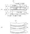
まだ半導体素子が搭載されていない状態のプリント配線板は、コア基板の一面側に設けられた導体回路層により生じる応力と、他面側に設けられた導体回路層により生じる応力のバランスによって、半導体素子が搭載される側の面を内側にして反るプラス反り(図15A参照)と、半導体素子が搭載される側の面を外側にして反るマイナス反り(図15B参照)の何れかが生じる。
これに対し、プリント配線板上に半導体素子を搭載した状態の半導体装置が反る方向は、半導体素子の線膨張係数と剛性が支配的に作用するため、通常は、半導体素子が搭載された側の面を外側にして反るマイナス反りになる。半導体装置のマイナス反りが大きすぎると、半導体装置の素子搭載面とは反対側の面をマザーボードに二次接続する際に接続位置がずれて接続不良が生じるという問題や、冷熱衝撃試験において半導体素子中の配線層の破壊やプリント配線板と半導体素子を接続する半田バンプにクラックが生じ信頼性が低下する等の問題が生じやすい。
半導体装置(半導体パッケージ)の反りを解決する提案としては、特許文献1には、コア基板の表面Aと表面Bに、層間絶縁樹脂層と配線層とが少なくとも一層ずつ積層されたビルドアップ配線層が形成されたビルドアップ配線板において、半導体素子が実装される表面A側の層間絶縁樹脂層の平面方向の熱膨張係数が、実装基板に実装される表面B側の層間絶縁樹脂層の平面方向の熱膨張係数より大きいことを特徴とする半導体装置用ビルドアップ配線板が記載されている。
Semiconductor devices (semiconductor packages) used in electronic devices are continuously miniaturized, densified and highly functionalized. For example, PoP (Package on Package), SiP (System in Package), FCBGA (Flip Chip Ball Grid Array). ) Etc. are known. With the progress of miniaturization and high density of such semiconductor devices, high-level miniaturization and thinning have been required for semiconductor elements and printed wiring boards constituting the semiconductor devices.
Generally, a printed circuit board is configured by providing a conductor circuit layer on a core substrate, particularly a conductor circuit layer that has been multilayered by build-up in recent years, and a semiconductor element is mounted on the conductor circuit layer of the printed circuit board. Are connected to form a semiconductor device.
As a method for thinning the printed wiring board, it is effective to thin the core substrate as the support. However, the linear expansion coefficient of the core substrate (usually about 8 to 15 ppm) is larger than the linear expansion coefficient of the semiconductor element (usually about 3 to 4 ppm), and the linear expansion coefficient of the conductor circuit layer (usually about the thermal expansion coefficient of the core substrate) Therefore, a stress is generated inside the printed wiring board or the semiconductor device due to the difference in coefficient of linear expansion between these portions. For this reason, when the core substrate is thinned, there is a problem that the stress caused by the difference in the linear expansion coefficient of each part becomes superior to the rigidity of the core substrate, and warpage is likely to occur.
A printed wiring board in which a semiconductor element is not yet mounted is based on the balance between the stress generated by the conductor circuit layer provided on one side of the core substrate and the stress generated by the conductor circuit layer provided on the other side. Either a positive warp (see FIG. 15A) that warps with the surface on which the element is mounted inward (see FIG. 15A) or a negative warp (see FIG. 15B) that warps with the surface on which the semiconductor element is mounted on the outside occurs. .
On the other hand, the direction in which the semiconductor device in which the semiconductor element is mounted on the printed wiring board is warped mainly depends on the linear expansion coefficient and rigidity of the semiconductor element. It becomes a negative warp that warps with the side of the outer side facing out. If the negative warpage of the semiconductor device is too large, the connection position may be shifted when the surface opposite to the element mounting surface of the semiconductor device is secondarily connected to the mother board, resulting in poor connection, or the semiconductor element in the thermal shock test. Problems such as destruction of the internal wiring layer, cracks in the solder bumps connecting the printed wiring board and the semiconductor element, and reduced reliability are likely to occur.
As a proposal for solving the warp of a semiconductor device (semiconductor package),
しかし、特許文献1の発明によって得られる半導体装置の反りを軽減する効果は必ずしも充分ではない。
また、特許文献1の発明のようにプリント配線板(ビルドアップ配線板)のビルドアップ層に含まれる層間絶縁樹脂層の線膨張係数を調節して反りを防止しようとする方法においては、コア基板の一面側とその反対面側に積層される層間絶縁樹脂層の数の違いによっても反り軽減の程度が変動し、また層間絶縁樹脂層を用いない両面板の場合は利用できないなど、配線層の数が制約される。また、層間絶縁樹脂層にガラスクロスを含むプリプレグを用いるため、レーザーによるビア加工の不具合が生じ、ビア間の信頼性に影響を及ぼすおそれがある。
さらに、プリント配線板のビルドアップ層には層間絶縁樹脂層だけでなく配線層(所定の回路パターンを形成する金属層)も含まれており、当該配線層の線膨張係数も反りに影響する。配線層は均一な連続膜ではなく、各層ごとに回路パターンの形状や面積が異なるため、応力に与える影響を予測することが困難である。
また、プリント配線板の配線層の数や回路パターンの形状が設計上の制約を受けるためにコア基板の一面側とその反対面側の応力が拮抗する場合があり、その場合には、同じ仕様のプリント配線板であっても個々の製品ごとに反りの方向が不規則となり、プラス反りとマイナス反りの両方が発生する場合がある。
従って、特許文献1の発明では半導体装置の反りを軽減するための制御が難しい。
However, the effect of reducing the warp of the semiconductor device obtained by the invention of
Further, in the method of preventing warpage by adjusting the linear expansion coefficient of the interlayer insulating resin layer included in the buildup layer of the printed wiring board (buildup wiring board) as in the invention of
Further, the build-up layer of the printed wiring board includes not only an interlayer insulating resin layer but also a wiring layer (a metal layer forming a predetermined circuit pattern), and the linear expansion coefficient of the wiring layer also affects the warpage. Since the wiring layer is not a uniform continuous film, and the shape and area of the circuit pattern differs from layer to layer, it is difficult to predict the effect on the stress.
Also, because the number of printed wiring board layers and circuit pattern shapes are subject to design constraints, the stress on one side of the core board and the opposite side may antagonize. Even in the case of printed wiring boards, the direction of warpage is irregular for each product, and both positive warpage and negative warpage may occur.
Therefore, in the invention of
上記実情に鑑み、本発明は層間絶縁樹脂層の物性や層数にとらわれずに下記いずれかの目的の少なくとも一つを達成することを目的とする。
本発明の第一の目的は、半導体装置のマイナス反りを充分に軽減又は防止することができる絶縁性基板又は金属張積層板を提供することにある。
また本発明の第二の目的は、半導体装置のマイナス反りを軽減又は防止するための制御が容易な絶縁性基板又は金属張積層板を提供することにある。
また本発明の第三の目的は、上記本発明の絶縁性基板又は金属張積層板を用いて作成された、反りが制御されたプリント配線板を提供することにある。
また本発明の第四の目的は、上記本発明の絶縁性基板又は金属張積層板を用いて作成された、反りが軽減又は防止された半導体装置を提供することにある。
In view of the above circumstances, an object of the present invention is to achieve at least one of the following objects regardless of the physical properties and the number of layers of the interlayer insulating resin layer.
A first object of the present invention is to provide an insulating substrate or a metal-clad laminate that can sufficiently reduce or prevent minus warpage of a semiconductor device.
A second object of the present invention is to provide an insulating substrate or a metal-clad laminate that can be easily controlled to reduce or prevent minus warpage of a semiconductor device.
A third object of the present invention is to provide a printed wiring board with controlled warpage, which is produced using the insulating substrate or metal-clad laminate of the present invention.
A fourth object of the present invention is to provide a semiconductor device which is produced by using the insulating substrate or metal-clad laminate of the present invention and in which warpage is reduced or prevented.
本発明の絶縁性基板は、1層以上の繊維基材層及び2層以上の樹脂層を含み、両面の最外層が樹脂層である積層体の硬化物からなる絶縁性基板であって、
前記絶縁性基板に含まれる前記繊維基材層を一面側から順にCx(xは1〜nで表される整数であり、nは繊維基材層の数である。)とし、
前記絶縁性基板の全体厚み(B3)を前記繊維基材層の数(n)で均等に分割し、分割した各領域の厚み(B4)をさらに均等に2分割する位置を繊維基材層の基準位置とし、当該各々の基準位置を一面側から順にAx(xは1〜nで表される整数であり、nは繊維基材層の数である。)としたときに、
前記繊維基材層のうち少なくとも1つが、対応する順位の基準位置よりも一面側又は他面側に偏在し、異なる方向に偏在しているものがないことを特徴とするものである。
The insulating substrate of the present invention is an insulating substrate comprising a cured product of a laminate including one or more fiber base layers and two or more resin layers, the outermost layers on both sides being resin layers,
The fiber base material layer contained in the insulating substrate is Cx (x is an integer represented by 1 to n, and n is the number of fiber base material layers) in order from one surface side.
The overall thickness (B3) of the insulating substrate is equally divided by the number (n) of the fiber base layers, and the thickness (B4) of each divided region is further divided into two equal parts by the fiber base layer. When the reference position is set to Ax (x is an integer represented by 1 to n and n is the number of fiber base layers) in order from one surface side to the reference position,
At least one of the fiber base layers is unevenly distributed on one surface side or the other surface side with respect to the reference position of the corresponding order, and there is no one unevenly distributed in a different direction.
また本発明の金属張積層板は、前記本発明の絶縁性基板の少なくとも一面側に金属箔層が設けられていることを特徴とするものである。 The metal-clad laminate of the present invention is characterized in that a metal foil layer is provided on at least one side of the insulating substrate of the present invention.
また本発明のプリント配線板は、前記本発明の絶縁性基板の少なくとも一面に、1層又は2層以上の導体回路層が設けられていることを特徴とするものである。 The printed wiring board of the present invention is characterized in that one or more conductor circuit layers are provided on at least one surface of the insulating substrate of the present invention.
また本発明の半導体装置は、前記本発明のプリント配線板の導体回路層上に、半導体素子を搭載してなることを特徴とするものである。 The semiconductor device of the present invention is characterized in that a semiconductor element is mounted on the conductor circuit layer of the printed wiring board of the present invention.
本発明によれば、絶縁性基板が含む少なくとも1つの繊維基材層が、当該繊維基材層に対応する順位の基準位置よりも一面側又は他面側に偏在し、異なる方向に偏在している繊維基材層がないことによって、当該絶縁性基板及びこの絶縁性基板を用いたプリント配線板が、前記繊維基材層が偏在する方向を外側にして反るか又は平坦に成形され、反りの方向や程度を制御することができる。従って、当該絶縁性基板又は当該プリント配線板に含まれる前記繊維基材層が偏在する方向を、半導体素子が搭載される面とは反対側を向くように合わせることによって、半導体素子が搭載される前のプリント配線板が意図的にプラス反り又は平坦の状態に制御され、その結果、当該プリント配線板に半導体素子を搭載した半導体装置のマイナス反りが軽減され又は完全に防止される。
また、本発明によれば、半導体装置の反りを制御するために導体回路層の数や回路パターンなどの回路設計を制約しないため、設計の自由度が高い。
According to the present invention, at least one fiber base layer included in the insulating substrate is unevenly distributed on one side or the other side of the reference position of the order corresponding to the fiber base layer, and is unevenly distributed in different directions. When there is no fiber base material layer, the insulating substrate and the printed wiring board using the insulating substrate are warped with the fiber base material layer being unevenly distributed or flatly formed, and warped. Can control the direction and degree. Therefore, the semiconductor element is mounted by matching the direction in which the fiber base layer included in the insulating substrate or the printed wiring board is unevenly distributed so as to face the side opposite to the surface on which the semiconductor element is mounted. The previous printed wiring board is intentionally controlled to be in a plus warp or flat state, and as a result, the minus warp of the semiconductor device in which the semiconductor element is mounted on the printed wiring board is reduced or completely prevented.
Further, according to the present invention, since the circuit design such as the number of conductor circuit layers and the circuit pattern is not restricted in order to control the warp of the semiconductor device, the degree of freedom in design is high.
1.絶縁性基板
本発明の絶縁性基板は、1層以上の繊維基材層及び2層以上の樹脂層を含み、両面の最外層が樹脂層である積層体の硬化物からなる絶縁性基板であって、
前記絶縁性基板に含まれる前記繊維基材層を一面側から順にCx(xは1〜nで表される整数であり、nは繊維基材層の数である。)とし、
前記絶縁性基板の全体厚み(B3)を前記繊維基材層の数(n)で均等に分割し、分割した各領域の厚み(B4)をさらに均等に2分割する位置を繊維基材層の基準位置とし、当該各々の基準位置を一面側から順にAx(xは1〜nで表される整数であり、nは繊維基材層の数である。)としたときに、
前記繊維基材層のうち少なくとも1つが、対応する順位の基準位置よりも一面側又は他面側に偏在し、異なる方向に偏在しているものがないことを特徴とする。
1. Insulating substrate The insulating substrate of the present invention is an insulating substrate comprising a cured product of a laminate including one or more fiber base layers and two or more resin layers, and the outermost layers on both sides are resin layers. And
The fiber base material layer contained in the insulating substrate is Cx (x is an integer represented by 1 to n, and n is the number of fiber base material layers) in order from one surface side.
The overall thickness (B3) of the insulating substrate is equally divided by the number (n) of the fiber base layers, and the thickness (B4) of each divided region is further divided into two equal parts by the fiber base layer. When the reference position is set to Ax (x is an integer represented by 1 to n and n is the number of fiber base layers) in order from one surface side to the reference position,
It is characterized in that at least one of the fiber base layers is unevenly distributed on one surface side or the other surface side with respect to the reference position of the corresponding order, and none is unevenly distributed in different directions.
前記基準位置は、換言すると、本発明の絶縁性基板の一面側から下記式:
基準位置=(全体厚み(B3)÷繊維基材層の数(n))×(繊維基材層の順位を表す整数(Cx)−0.5)
で算出される高さの位置である。
なお、本発明の絶縁性基板が複数の繊維基材層を有する場合は、少なくとも1つの繊維基材層が対応する順位の基準位置よりも一面側又は他面側に偏在していれば、その他の繊維基材層は対応する順位の基準位置上に設けられていても良い。
In other words, the reference position is expressed by the following formula from one side of the insulating substrate of the present invention:
Reference position = (total thickness (B3) ÷ number of fiber base layers (n)) × (integer (Cx) −0.5 representing the rank of fiber base layers)
This is the height position calculated by.
In addition, when the insulating substrate of the present invention has a plurality of fiber base layers, if at least one fiber base layer is unevenly distributed on one side or the other side of the reference position of the corresponding order, other The fiber base layer may be provided on the reference position of the corresponding order.
本発明の絶縁性基板は、その製造過程において加熱加圧成形後冷却される時に、繊維基材層の偏在する方向を外側にして反る性質がある。繊維基材層の線膨張係数よりも樹脂層の線膨張係数の方が大きいため、加熱加圧成形時の応力フリーから常温まで冷却された際に、樹脂層は繊維基材層より縮む。このため、絶縁性基板全体として、繊維基材層が偏在する方向を外側にして反る。
本発明の絶縁性基板は、この性質を利用して、繊維基材層の位置を調整することにより、絶縁性基板の反りを制御することができる。
The insulating substrate of the present invention has the property of warping with the direction of uneven distribution of the fiber base layer being outside when cooled after heating and pressing in the production process. Since the linear expansion coefficient of the resin layer is larger than the linear expansion coefficient of the fiber base material layer, the resin layer shrinks from the fiber base material layer when cooled from the stress-free state at the time of heat and pressure molding to room temperature. For this reason, the insulating substrate as a whole warps with the direction in which the fiber base layer is unevenly distributed outward.
The insulating substrate of this invention can control the curvature of an insulating substrate by adjusting the position of a fiber base material layer using this property.
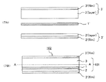
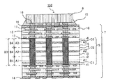
以下、本発明の絶縁性基板について図をもとに詳細に説明する。
図1は、本発明の絶縁性基板の一例として、1層の繊維基材層と2層の樹脂層からなるものの断面を模式的に示した図である。図1Aに示す絶縁性基板111は、一面側から樹脂層r1、繊維基材層C1、樹脂層r2の順に積層した層構成を有する。繊維基材層C1は、対応する順位の基準位置A1−A1線よりも一面側(樹脂層r1側)の方向に偏在する。絶縁性基板111は、繊維基材層を1層しか有しないので、全体厚みB3を繊維基材層の数で均等に分割した各領域の厚みB4は、全体厚みB3と同じ厚みである。
図1Aに示す絶縁性基板111は、製造過程において加熱加圧成形後冷却される時に、樹脂層が繊維基材層よりも大きく収縮するため、常温では、図1Bに示すように、繊維基材層C1が偏在する方向を外側にして反る性質がある。
Hereinafter, the insulating substrate of the present invention will be described in detail with reference to the drawings.
FIG. 1 is a diagram schematically showing a cross section of an example of an insulating substrate of the present invention, which is composed of one fiber base layer and two resin layers. The insulating
In the insulating
図2は、1層の繊維基材層を含む本発明の絶縁性基板の他の一例として、1層の繊維基材層と3層の樹脂層からなる絶縁性基板の断面を模式的に示した図である。図2Aに示す絶縁性基板112は、一面側から樹脂層r1、繊維基材層C1、樹脂層r2、r3の順に積層した層構成を有する。繊維基材層C1は、対応する順位の基準位置A1−A1線よりも一面側(樹脂層r1側)に偏在する。絶縁性基板112は繊維基材層を1層しか有しないので、全体厚みB3を繊維基材層の数で均等に分割した各領域の厚みB4は、全体厚みB3と同じ厚みである。
図2Aに示す絶縁性基板112は、製造過程において加熱加圧成形後冷却される時に、樹脂層が繊維基材層よりも大きく収縮するため、常温では、図2Bに示すように、繊維基材層C1が偏在する方向を外側にして反る性質がある。
本発明の絶縁性基板は、図2Aに示す樹脂層r2、r3や、後述する図3Aに示す樹脂層r2、r3のように、複数の樹脂層が積層してなる部分を含んでいても良い。本発明において複数の樹脂層が積層するとは、絶縁性基板を硬化させる前の製造段階において複数の樹脂層を積層することを意味し、硬化後の絶縁性基板断面においては、複数の樹脂層の境界面を確認できなくても良い。
FIG. 2 schematically shows a cross section of an insulating substrate composed of one fiber substrate layer and three resin layers as another example of the insulating substrate of the present invention including one fiber substrate layer. It is a figure. The insulating
In the insulating
The insulating substrate of the present invention may include a portion formed by laminating a plurality of resin layers, such as resin layers r2 and r3 shown in FIG. 2A and resin layers r2 and r3 shown in FIG. 3A described later. . In the present invention, to laminate a plurality of resin layers means to laminate a plurality of resin layers in the manufacturing stage before curing the insulating substrate, and in the cross section of the insulating substrate after curing, The boundary surface may not be confirmed.
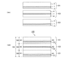
図3は、本発明の絶縁性基板の他の一例として、2層の繊維基材層と4層の樹脂層からなる絶縁性基板の断面を模式的に示した図である。図3Aに示す絶縁性基板113は、一面側から樹脂層r1、繊維基材層C1、樹脂層r2、r3、繊維基材層C2、樹脂層r4の順に積層した層構成を有する。繊維基材層C1は、対応する順位の基準位置A1−A1線よりも一面側(樹脂層r1側)に偏在し、繊維基材層C2も、対応する順位の基準位置A2−A2線よりも一面側(樹脂層r3側)に偏在し、即ち繊維基材層C1及びC2は同じ方向に偏在している。絶縁性基板113の全体厚みB3を繊維基材層の数で均等に分割した各領域、即ち全体厚みB3を2等分した各領域の厚みをB4として示す。繊維基材層C1及びC2は、両方とも一面側の厚みB4の領域内に存在し、他面側の厚みB4の領域内には繊維基材層は存在しない。
図3Aに示す絶縁性基板113は、製造過程において加熱加圧成形後冷却される時に、樹脂層が繊維基材層よりも大きく収縮するため、常温では、図3Bに示すように繊維基材層C1及びC2が偏在する方向を外側にして反る性質がある。
FIG. 3 is a diagram schematically showing a cross-section of an insulating substrate composed of two fiber base layers and four resin layers as another example of the insulating substrate of the present invention. The insulating
When the insulating
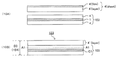
図4は、2層の繊維基材層と4層の樹脂層を含む本発明の絶縁性基板の他の一例の断面を模式的に示した図である。図4Aに示す絶縁性基板114は、一面側から樹脂層r1、繊維基材層C1、樹脂層r2、r3、繊維基材層C2、樹脂層r4の順に積層した層構成を有する。繊維基材層C1は、対応する順位の基準位置A1−A1線上に存在し、繊維基材層C2は、対応する順位の基準位置A2−A2線よりも一面側(樹脂層r3側)に偏在する。絶縁性基板114の全体厚みB3を繊維基材層の数で均等に分割した各領域、即ち全体厚みB3を2等分した各領域の厚みをB4として示す。繊維基材層C1及びC2は、それぞれ厚みB4の各領域内に1つずつ存在する。
図4Aに示す絶縁性基板114は、製造過程において加熱加圧成形後冷却される時に、樹脂層が繊維基材層よりも大きく収縮するため、常温では、図4Bに示すように繊維基材層C2が偏在する方向を外側にして反る性質がある。
FIG. 4 is a view schematically showing a cross section of another example of the insulating substrate of the present invention including two fiber base layers and four resin layers. The insulating
When the insulating
図5は、本発明の絶縁性基板の他の一例として、3層の繊維基材層と6層の樹脂層からなる絶縁性基板の断面を模式的に示した図である。図5Aに示す絶縁性基板115は、一面側から樹脂層r1、繊維基材層C1、樹脂層r2、r3、繊維基材層C2、樹脂層r4、r5、繊維基材層C3、樹脂層r6の順に積層した層構成を有する。繊維基材層C1、C2、C3のうち、最も一面側に位置する繊維基材層C1は、対応する順位の基準位置A1−A1線よりも一面側(樹脂層r1側)に偏在し、繊維基材層C2及びC3は、それぞれ対応する順位の基準位置A2−A2線及びA3−A3線の上に存在する。絶縁性基板115の全体厚みB3を繊維基材層の数で均等に分割した各領域、即ち全体厚みB3を3等分した各領域の厚みをB4として示す。繊維基材層C1、C2、C3は、それぞれ厚みB4の各領域内に1つずつ存在する。
図5Aに示す絶縁性基板115は、製造過程において加熱加圧成形後冷却される時に、樹脂層が繊維基材層よりも大きく収縮するため、常温では、図5Bに示すように繊維基材層C1が偏在する方向を外側にして反る性質がある。
FIG. 5 is a view schematically showing a cross-section of an insulating substrate composed of three fiber base layers and six resin layers as another example of the insulating substrate of the present invention. The insulating
When the insulating
図6は、3層の繊維基材層と6層の樹脂層を含む本発明の絶縁性基板の他の一例の断面を模式的に示した図である。図6Aに示す絶縁性基板116は、一面側から樹脂層r1、繊維基材層C1、樹脂層r2、r3、繊維基材層C2、樹脂層r4、r5、繊維基材層C3、樹脂層r6の順に積層した層構成を有する。繊維基材層C1、C2、C3のうち、最も一面側に位置する繊維基材層C1は、対応する順位の基準位置A1−A1線よりも一面側(樹脂層r1側)に偏在し、最も他面側に位置する繊維基材層C3は、対応する順位の基準位置A3−A3線よりも一面側(樹脂層r5側)に偏在し、即ち繊維基材層C1及びC3は同じ方向に偏在している。繊維基材層C2は対応する順位の基準位置A2−A2線上に存在する。絶縁性基板116の全体厚みB3を繊維基材層の数で均等に分割した各領域、即ち全体厚みB3を3等分した各領域の厚みをB4として示す。繊維基材層C1、C2、C3は、それぞれ厚みB4の各領域内に1つずつ存在する。
図6Aに示す絶縁性基板116は、製造過程において加熱加圧成形後冷却される時に、樹脂層が繊維基材層よりも大きく収縮するため、常温では、図6Bに示すように繊維基材層C1及びC3が偏在する方向を外側にして反る性質がある。
FIG. 6 is a view schematically showing a cross section of another example of the insulating substrate of the present invention including three fiber base layers and six resin layers. The insulating
When the insulating
本発明の絶縁性基板は、特に限定はされないが、前記繊維基材層のうち少なくとも1つが、対応する順位の基準位置よりも一面側に偏在し、前記偏在する繊維基材層は、当該繊維基材層の一面側の樹脂充填領域の厚み(B5)と、当該繊維基材層の他面側の樹脂充填領域の厚み(B6)との比(B5/B6)が、0.1<B5/B6<1.2であることが好ましい。
なお、本発明において「樹脂充填領域」とは、繊維基材層の界面から隣の繊維基材層又は空気層までの界面までの距離を意味する。前記樹脂充填領域は、1層の樹脂層からなるものでも良いし、複数の樹脂層が積層してなるものであっても良い。また、本発明において「界面」とは、樹脂層と繊維基材層又は空気層との境界となる面の凹凸を平均化した平坦な面を意味する。
図1A、図2A、図3A、図4A、図5A及び図6Aに示す各絶縁性基板に、それぞれ偏在する繊維基材層を基準としたときのB5及びB6を示す。なお、図3Aに示す絶縁性基板113と図6Aに示す絶縁性基板116は、2つの繊維基材層が偏在するため、偏在する繊維基材層各々を基準としたB5及びB6を示す。
なお、本発明の絶縁性基板は、B5/B6が1以上となる場合があるが、これは、例えば図4Aに示す絶縁性基板114の場合や、図6Aに示す絶縁性基板116において繊維基材層C3を基準とした場合等が挙げられる。
本発明の絶縁性基板は、B5/B6が前記下限値未満の場合は、繊維基材層が極端に偏在することになるため、絶縁性基板の反りが大きくなりすぎることがある。一方、B5/B6が前記上限値を超える場合は、繊維基材層間の距離が大きすぎて、反りの制御が困難となることがある。よって、B5/B6が前記範囲内であると、繊維基材層がバランス良く配置されるため、絶縁性基板の反りの制御が容易になる。
The insulating substrate of the present invention is not particularly limited, but at least one of the fiber base layers is unevenly distributed on one surface side with respect to the reference position of the corresponding order, and the unevenly distributed fiber base layer includes the fibers The ratio (B5 / B6) of the thickness (B5) of the resin-filled region on the one surface side of the base material layer to the thickness (B6) of the resin-filled region on the other surface side of the fiber base material layer is 0.1 <B5 It is preferable that /B6<1.2.
In the present invention, the “resin-filled region” means the distance from the interface of the fiber base layer to the interface of the adjacent fiber base layer or air layer. The resin-filled region may be composed of a single resin layer or may be a laminate of a plurality of resin layers. In the present invention, the “interface” means a flat surface obtained by averaging the unevenness of the surface serving as the boundary between the resin layer and the fiber base layer or the air layer.
B5 and B6 are shown when the fiber substrate layer that is unevenly distributed on the respective insulating substrates shown in FIGS. 1A, 2A, 3A, 4A, 5A, and 6A is used as a reference. Note that the insulating
Note that the insulating substrate of the present invention may have B5 / B6 of 1 or more. For example, in the case of the insulating
In the insulating substrate of the present invention, when B5 / B6 is less than the lower limit value, since the fiber base layer is extremely unevenly distributed, the warping of the insulating substrate may be excessively large. On the other hand, when B5 / B6 exceeds the upper limit, the distance between the fiber base layers may be too large, and it may be difficult to control warpage. Therefore, when B5 / B6 is within the above range, the fiber base material layer is arranged in a well-balanced manner, so that the warpage of the insulating substrate can be easily controlled.
本発明の絶縁性基板は、特に限定はされないが、全体厚み(B3)を繊維基材層の数で均等に分割した厚みB4の各領域(以下、単に「厚みB4の領域」又は「B4領域」と称することがある。)内に、それぞれ1つの繊維基材層が存在することが、絶縁性基板の反りが大きくなり過ぎずに反りの制御を容易にする観点から好ましい。 The insulating substrate of the present invention is not particularly limited, but each region of thickness B4 (hereinafter simply referred to as “region of thickness B4” or “B4 region”) obtained by equally dividing the total thickness (B3) by the number of fiber base layers. In other words, it is preferable that one fiber base material layer be present in each of them from the viewpoint of facilitating the control of the warp without the warp of the insulating substrate becoming too large.
本発明の絶縁性基板は、特に限定はされないが、厚みB4の各領域のうち少なくとも1つが、1つの繊維基材層を、対応する順位の基準位置よりも一面側に偏在して有し、前記偏在する繊維基材層は、当該繊維基材層の一面側の界面から当該繊維基材層が属する厚みB4の領域の当該一面側の境界までの距離(B7)と、当該繊維基材層の他面側の界面から当該繊維基材層が属する厚みB4の領域の当該他面側の境界までの距離(B8)との比(B7/B8)が、0.1<B7/B8<0.9であることが、絶縁性基板の反りが大きくなり過ぎずに反りの制御を容易にする観点から好ましい。
図1A、図2A、図4A、図5A及び図6Aに示す各絶縁性基板に、それぞれ偏在する繊維基材層を基準としたときのB7及びB8を示す。なお、図3Aに示す絶縁性基板113のように、厚みB4の領域内に1つも繊維基材層が存在しない場合や複数の繊維基材層が存在する場合は、B7及びB8を特定することができない。図1Aに示す絶縁性基板111や図2Aに示す絶縁性基板112のように、繊維基材層を1層しか有しない絶縁性基板の場合は、B7及びB8は、それぞれ上述したB5及びB6と同じ値になる。
The insulating substrate of the present invention is not particularly limited, but at least one of the regions of thickness B4 has one fiber base layer that is unevenly distributed on the one surface side from the reference position of the corresponding order, The unevenly distributed fiber base layer includes a distance (B7) from an interface on one side of the fiber base layer to a boundary on the one side of a region of thickness B4 to which the fiber base layer belongs, and the fiber base layer. The ratio (B7 / B8) to the distance (B8) from the interface on the other surface side to the boundary on the other surface side of the region of thickness B4 to which the fiber base material layer belongs is 0.1 <B7 / B8 <0. .9 is preferable from the viewpoint of facilitating the control of the warp without the warp of the insulating substrate becoming too large.
B7 and B8 when the fiber base material layer unevenly distributed on the respective insulating substrates shown in FIG. 1A, FIG. 2A, FIG. 4A, FIG. 5A and FIG. In addition, like the insulating
また、本発明の絶縁性基板が複数の繊維基材層を有するものである場合は、前記複数の繊維基材層のうち最も一面側に位置するものが、対応する順位の基準位置よりも前記一面側に偏在して配置されていることが、絶縁性基板の反る方向を確実に制御する観点から好ましい。
同様の観点から、前記複数の繊維基材層のうち最も一面側に位置するものが、対応する順位の基準位置よりも前記一面側に偏在して配置され、且つ、最も他面側に位置するものが、対応する順位の基準位置よりも前記一面側に配置されていることが特に好ましい。
Moreover, when the insulating substrate of the present invention has a plurality of fiber base layers, the one located on the most surface side of the plurality of fiber base layers is more than the reference position of the corresponding order. It is preferable that it is unevenly distributed on one surface side from the viewpoint of surely controlling the warping direction of the insulating substrate.
From the same viewpoint, among the plurality of fiber base layers, the one located on the most one side is arranged unevenly on the one side with respect to the reference position of the corresponding order, and located on the other side most. It is particularly preferable that the object is arranged on the one surface side with respect to the reference position of the corresponding order.
本発明の絶縁性基板の全体厚み(B3)は、特に限定されないが、通常0.03〜0.5mm、好ましくは0.04〜0.4mmである。 The total thickness (B3) of the insulating substrate of the present invention is not particularly limited, but is usually 0.03 to 0.5 mm, preferably 0.04 to 0.4 mm.
本発明の絶縁性基板の全体厚み(B3)を繊維基材層の数で均等に分割した各領域の厚み(B4)は、特に限定されないが、通常5〜200μmである。 Although the thickness (B4) of each area | region which divided | segmented the whole thickness (B3) of the insulating board | substrate of this invention equally by the number of fiber base material layers is not specifically limited, Usually, it is 5-200 micrometers.
本発明の絶縁性基板が有する樹脂層は、熱硬化性、感光性等の硬化性樹脂組成物が硬化してなる層である。一方、本発明の絶縁性基板が有する繊維基材層は、繊維基材に前記硬化性樹脂組成物が含浸、硬化してなる層である。
また、本発明に用いられる絶縁性基板は、繊維基材層の一面側にある樹脂層と、他面側にある樹脂層とが異なる硬化性樹脂組成物で形成されていても良い。複数の樹脂層が隣接して積層する場合は、樹脂層同士の接着性に影響がない範囲で、隣り合う樹脂層は互いに異なる硬化性樹脂組成物で形成されていても良い。また、繊維基材層は、一面側の樹脂層又は他面側の樹脂層のいずれかを形成する硬化性樹脂組成物が含浸しているか、或いは、一面側の樹脂層を形成する樹脂が含浸し、他面側の樹脂層を形成する樹脂が含浸し、繊維基材の内部で2種類の樹脂が接触または混合していてもよい。
The resin layer of the insulating substrate of the present invention is a layer formed by curing a curable resin composition such as thermosetting and photosensitive properties. On the other hand, the fiber base material layer which the insulating substrate of the present invention has is a layer formed by impregnating and curing a fiber base material with the curable resin composition.
Moreover, the insulating board | substrate used for this invention may be formed with the curable resin composition from which the resin layer in the one surface side of a fiber base material layer differs from the resin layer in the other surface side. When a plurality of resin layers are laminated adjacent to each other, the adjacent resin layers may be formed of different curable resin compositions as long as the adhesiveness between the resin layers is not affected. Further, the fiber base layer is impregnated with a curable resin composition that forms either the resin layer on one side or the resin layer on the other side, or impregnated with a resin that forms the resin layer on the one side. And the resin which forms the resin layer of the other surface side may impregnate, and two types of resin may be contacting or mixing inside the fiber base material.
前記繊維基材としては、特に限定されないが、半導体装置の製造プロセス及び使用条件に耐えられる耐熱性を有する材料が選ばれる。そのような繊維基材としては、例えば、ガラス織布、ガラス不織布等のガラス繊維基材、ポリアミド樹脂繊維、芳香族ポリアミド樹脂繊維、全芳香族ポリアミド樹脂繊維等のポリアミド系樹脂繊維、ポリエステル樹脂繊維、芳香族ポリエステル樹脂繊維、全芳香族ポリエステル樹脂繊維等のポリエステル系樹脂繊維、ポリイミド樹脂繊維、フッ素樹脂繊維、ポリベンゾオキサゾール樹脂等を主成分とする織布または不織布で構成される合成繊維基材、クラフト紙、コットンリンター紙、リンターとクラフトパルプの混抄紙等を主成分とする紙基材等の有機繊維基材等の繊維基材、ポリエステル、ポリイミド等の樹脂フィルム等が挙げられる。これらの中でもガラス繊維基材が好ましい。これにより、絶縁性基板の強度を向上することができ、また、絶縁性基板の熱膨張係数を小さくすることができる。 The fiber substrate is not particularly limited, but a material having heat resistance that can withstand the manufacturing process and use conditions of the semiconductor device is selected. Examples of such fiber base materials include glass fiber base materials such as glass woven fabric and glass nonwoven fabric, polyamide resin fibers, aromatic polyamide resin fibers, polyamide resin fibers such as wholly aromatic polyamide resin fibers, and polyester resin fibers. Synthetic fiber base materials composed of woven or non-woven fabrics mainly composed of polyester resin fibers such as aromatic polyester resin fibers and wholly aromatic polyester resin fibers, polyimide resin fibers, fluororesin fibers, polybenzoxazole resins, etc. And fiber base materials such as organic fiber base materials such as paper base materials mainly composed of kraft paper, cotton linter paper, mixed paper of linter and kraft pulp, and resin films such as polyester and polyimide. Among these, a glass fiber base material is preferable. Thereby, the strength of the insulating substrate can be improved, and the thermal expansion coefficient of the insulating substrate can be reduced.
ガラス繊維基材を構成するガラスとしては、例えばEガラス、Cガラス、Aガラス、Sガラス、Dガラス、NEガラス、Tガラス、Hガラス、石英ガラス等が挙げられる。これらの中でも、特にEガラス、Tガラスを用いる場合に、ガラス繊維基材の高弾性化を達成することができ、熱膨張係数も小さくすることができる。 Examples of the glass constituting the glass fiber substrate include E glass, C glass, A glass, S glass, D glass, NE glass, T glass, H glass, and quartz glass. Among these, particularly when E glass or T glass is used, high elasticity of the glass fiber substrate can be achieved, and the thermal expansion coefficient can also be reduced.
前記繊維基材の厚さは特に限定されないが、通常5〜200μm程度の厚さのものが用いられ、特にプリント配線板のコア層(絶縁性基板の部分)を薄くしたい場合には5〜100μm程度とすることが好ましい。 Although the thickness of the fiber base material is not particularly limited, a thickness of about 5 to 200 μm is usually used. In particular, when it is desired to reduce the core layer (part of the insulating substrate) of the printed wiring board, the thickness is 5 to 100 μm. It is preferable to set the degree.
前記硬化性樹脂組成物としては、熱硬化性、感光性等の硬化性樹脂組成物が用いられるが、通常は熱硬化性樹脂組成物が用いられる。熱硬化性樹脂組成物は、通常、熱硬化性樹脂、硬化剤、充填材等を含有する。 As the curable resin composition, a curable resin composition such as a thermosetting resin or a photosensitive resin is used, but a thermosetting resin composition is usually used. The thermosetting resin composition usually contains a thermosetting resin, a curing agent, a filler, and the like.
熱硬化性樹脂としては、エポキシ樹脂、シアネート樹脂、ビスマレイミド樹脂、フェノール樹脂、ベンゾオキサジン樹脂、ポリアミド樹脂、ポリイミド樹脂、ポリアミドイミド樹脂等が用いられ、通常は、エポキシ樹脂に他の熱硬化性樹脂を適宜組み合わせて用いられる。
前記エポキシ樹脂としては、特に限定されないが、実質的にハロゲン原子を含まないエポキシ樹脂であり、例えば、ビスフェノールA型エポキシ樹脂、ビスフェノールF型エポキシ樹脂、ビスフェノールE型エポキシ樹脂、ビスフェノールS型エポキシ樹脂、ビスフェノールZ型エポキシ樹脂(4,4’−シクロヘキシジエンビスフェノール型エポキシ樹脂)、ビスフェノールP型エポキシ樹脂(4,4’−(1,4−フェニレンジイソプリジエン)ビスフェノール型エポキシ樹脂)、ビスフェノールM型エポキシ樹脂(4,4’−(1,3−フェニレンジイソプリジエン)ビスフェノール型エポキシ樹脂)等のビスフェノール型エポキシ樹脂、フェノールノボラック型エポキシ樹脂、クレゾールノボラック型エポキシ樹脂等のノボラック型エポキシ樹脂、ビフェニル型エポキシ樹脂、キシリレン型エポキシ樹脂、フェノールアラルキル型エポキシ樹脂、ビフェニルアラルキル型エポキシ樹脂、ビフェニルジメチレン型エポキシ樹脂、ビフェニルアラルキル型ノボラックエポキシ樹脂、トリスフェノールメタンノボラック型エポキシ樹脂、1,1,2,2−(テトラフェノール)エタンのグリシジルエーテル類、3官能、又は4官能のグリシジルアミン類、テトラメチルビフェニル型エポキシ樹脂等のアリールアルキレン型エポキシ樹脂、ナフタレン骨格変性クレゾールノボラック型エポキシ樹脂、メトキシナフタレン変性クレゾールノボラック型エポキシ樹脂、メトキシナフタレンジメチレン型エポキシ樹脂、ナフトールアルキレン型エポキシ樹脂等のナフタレン型エポキシ樹脂、アントラセン型エポキシ樹脂、フェノキシ型エポキシ樹脂、ジシクロペンタジエン型エポキシ樹脂、ノルボルネン型エポキシ樹脂、アダマンタン型エポキシ樹脂、フルオレン型エポキシ樹脂、上記エポキシ樹脂をハロゲン化した難燃化エポキシ樹脂等が挙げられる。これらの中の1種類を単独で用いることもできるし、異なる重量平均分子量を有する2種類以上を併用することもでき、1種類又は2種類以上と、それらのプレポリマーを併用することもできる。
As the thermosetting resin, epoxy resin, cyanate resin, bismaleimide resin, phenol resin, benzoxazine resin, polyamide resin, polyimide resin, polyamideimide resin, etc. are used. Are used in appropriate combination.
The epoxy resin is not particularly limited, but is an epoxy resin that does not substantially contain a halogen atom. For example, bisphenol A type epoxy resin, bisphenol F type epoxy resin, bisphenol E type epoxy resin, bisphenol S type epoxy resin, Bisphenol Z type epoxy resin (4,4′-cyclohexyldiene bisphenol type epoxy resin), bisphenol P type epoxy resin (4,4 ′-(1,4-phenylenediisopridiene) bisphenol type epoxy resin), bisphenol M Type epoxy resins (4,4 '-(1,3-phenylenediisopridiene) bisphenol type epoxy resins) and other bisphenol type epoxy resins, phenol novolac type epoxy resins, and cresol novolak type epoxy resins. Si resin, biphenyl type epoxy resin, xylylene type epoxy resin, phenol aralkyl type epoxy resin, biphenyl aralkyl type epoxy resin, biphenyl dimethylene type epoxy resin, biphenyl aralkyl type novolac epoxy resin, trisphenol methane novolak type epoxy resin, 1,1 , 2,2- (tetraphenol) ethane glycidyl ethers, trifunctional or tetrafunctional glycidyl amines, arylalkylene type epoxy resins such as tetramethylbiphenyl type epoxy resins, naphthalene skeleton modified cresol novolac type epoxy resins, methoxy Naphthalene-modified epoxy resin such as naphthalene-modified cresol novolac type epoxy resin, methoxynaphthalene dimethylene type epoxy resin, naphthol alkylene type epoxy resin, Anthracene type epoxy resins, phenoxy type epoxy resins, dicyclopentadiene type epoxy resins, norbornene type epoxy resins, adamantane type epoxy resins, fluorene type epoxy resins, flame-retarded epoxy resin or the like halogenated epoxy resins. One of these can be used alone, two or more having different weight average molecular weights can be used in combination, and one or two or more of these prepolymers can be used in combination.
これらのエポキシ樹脂の中でもノボラック型エポキシ樹脂が好ましく、その中でもビフェニルアラルキル型ノボラックエポキシ樹脂がより好ましく、その中でもビフェニルジメチレン型エポキシ樹脂が特に好ましい。
ビフェニルアラルキル型ノボラックエポキシ樹脂とは、繰返し単位中に一つ以上のビフェニルアルキレン基を有するエポキシ樹脂をいう。例えばキシリレン型エポキシ樹脂、ビフェニルジメチレン型エポキシ樹脂等が挙げられる。ビフェニルジメチレン型エポキシ樹脂は、例えば、下記式(I)で示すことができる。
Among these epoxy resins, novolac type epoxy resins are preferable, and among them, biphenyl aralkyl type novolac epoxy resins are more preferable, and among them, biphenyl dimethylene type epoxy resins are particularly preferable.
The biphenyl aralkyl type novolak epoxy resin refers to an epoxy resin having one or more biphenyl alkylene groups in a repeating unit. For example, a xylylene type epoxy resin, a biphenyl dimethylene type epoxy resin, etc. are mentioned. The biphenyl dimethylene type epoxy resin can be represented by, for example, the following formula (I).

前記式(I)で示されるビフェニルジメチレン型エポキシ樹脂の平均繰返し単位数nは、特に限定されないが、1〜10が好ましく、特に2〜5が好ましい。平均繰返し単位数nが前記下限値未満であるとビフェニルジメチレン型エポキシ樹脂が結晶化しやすくなり、汎用溶媒に対する溶解性が低下するため取り扱いが困難になる場合がある。また、平均繰返し単位数nが前記上限値を超えると樹脂の流動性が低下し、成形不良等の原因になる場合がある。 The average repeating unit number n of the biphenyl dimethylene type epoxy resin represented by the formula (I) is not particularly limited, but is preferably 1 to 10, and particularly preferably 2 to 5. If the average repeating unit number n is less than the lower limit, the biphenyldimethylene type epoxy resin is likely to be crystallized, and the solubility in general-purpose solvents may be reduced, which may make handling difficult. On the other hand, if the average number of repeating units n exceeds the upper limit, the fluidity of the resin is lowered, which may cause molding defects.
エポキシ樹脂の分子量は特に限定されないが、ノボラック型エポキシ樹脂を用いる場合には、その重量平均分子量が5.0×10²〜2.0×10⁴の範囲であることが好ましい。ノボラック型エポキシ樹脂の重量平均分子量は、例えばGPC(ゲルパーミエーションクロマトグラフィー、標準物質:ポリスチレン換算)で測定することができる。
また、エポキシ樹脂の含有量は特に限定されないが、熱硬化性樹脂組成物の固形分基準で1〜65重量%が好ましい。
Although the molecular weight of an epoxy resin is not specifically limited, When using a novolak-type epoxy resin, it is preferable that the weight average molecular weight is the range of 5.0 * 10 < 2 > -2.0 * 10 < 4 >. The weight average molecular weight of the novolak type epoxy resin can be measured, for example, by GPC (gel permeation chromatography, standard substance: converted to polystyrene).
Moreover, although content of an epoxy resin is not specifically limited, 1 to 65 weight% is preferable on the solid content basis of a thermosetting resin composition.
本発明の熱硬化性樹脂組成物にシアネート樹脂を含ませることにより、難燃性を向上させ、熱膨張係数を小さくし、さらに、樹脂層の電気特性(低誘電率、低誘電正接)等を向上させることができ、前記シアネート樹脂は、特に限定されないが、例えば、ハロゲン化シアン化合物とフェノール類やナフトール類とを反応させ、必要に応じて加熱等の方法でプレポリマー化することにより得ることができる。また、このようにして調製された市販品を用いることもできる。 By including a cyanate resin in the thermosetting resin composition of the present invention, the flame retardancy is improved, the thermal expansion coefficient is reduced, and the electrical properties (low dielectric constant, low dielectric loss tangent) of the resin layer are improved. The cyanate resin is not particularly limited. For example, the cyanate resin can be obtained by reacting a halogenated cyanide compound with phenols or naphthols and, if necessary, prepolymerizing by a method such as heating. Can do. Moreover, the commercial item prepared in this way can also be used.
前記シアネート樹脂の種類としては、特に限定されないが、例えば、ノボラック型シアネート樹脂、ビスフェノールA型シアネート樹脂、ビスフェノールE型シアネート樹脂、テトラメチルビスフェノールF型シアネート樹脂等のビスフェノール型シアネート樹脂、ジシクロペンタジエン型シアネート樹脂、ビフェニルアラルキル型シアネート樹脂、及びナフトールアラルキル型シアネート樹脂等を挙げることができる。ノボラック型シアネート樹脂は、樹脂層の熱膨張係数を小さくすることができ、樹脂層の機械的強度、電気特性(低誘電率、低誘電正接)にも優れる。 The type of cyanate resin is not particularly limited. For example, bisphenol cyanate resin such as novolac type cyanate resin, bisphenol A type cyanate resin, bisphenol E type cyanate resin, tetramethylbisphenol F type cyanate resin, dicyclopentadiene type Cyanate resin, biphenyl aralkyl type cyanate resin, naphthol aralkyl type cyanate resin and the like can be mentioned. The novolac-type cyanate resin can reduce the thermal expansion coefficient of the resin layer, and is excellent in the mechanical strength and electrical characteristics (low dielectric constant, low dielectric loss tangent) of the resin layer.
前記シアネート樹脂は、分子内に2個以上のシアネート基(−O−CN)を有することが好ましい。例えば、2,2’−ビス(4−シアナトフェニル)イソプロピリデン、1,1’−ビス(4−シアナトフェニル)エタン、ビス(4−シアナト−3,5−ジメチルフェニル)メタン、1,3−ビス(4−シアナトフェニル−1−(1−メチルエチリデン))ベンゼン、ジシクロペンタジエン型シアネートエステル、フェノールノボラック型シアネートエステル、ビス(4−シアナトフェニル)チオエーテル、ビス(4−シアナトフェニル)エーテル、1,1,1−トリス(4−シアナトフェニル)エタン、トリス(4−シアナトフェニル)ホスファイト、ビス(4−シアナトフェニル)スルホン、2,2−ビス(4−シアナトフェニル)プロパン、1,3−、1,4−、1,6−、1,8−、2,6−又は2,7−ジシアナトナフタレン、1,3,6−トリシアナトナフタレン、4,4−ジシアナトビフェニル、及びフェノールノボラック型、クレゾールノボラック型の多価フェノール類と、ハロゲン化シアンとの反応で得られるシアネート樹脂、ナフトールアラルキル型の多価ナフトール類と、ハロゲン化シアンとの反応で得られるシアネート樹脂等が挙げられる。これらの中で、フェノールノボラック型シアネート樹脂が難燃性、及び低熱膨張性に優れ、2,2−ビス(4−シアナトフェニル)イソプロピリデン、及びジシクロペンタジエン型シアネートエステルが架橋密度の制御、及び耐湿信頼性に優れている。特に、フェノールノボラック型シアネート樹脂が低熱膨張性の点から好ましい。また、更に他のシアネート樹脂を1種類あるいは2種類以上併用したりすることもでき、特に限定されない。 The cyanate resin preferably has two or more cyanate groups (—O—CN) in the molecule. For example, 2,2′-bis (4-cyanatophenyl) isopropylidene, 1,1′-bis (4-cyanatophenyl) ethane, bis (4-cyanato-3,5-dimethylphenyl) methane, 3-bis (4-cyanatophenyl-1- (1-methylethylidene)) benzene, dicyclopentadiene type cyanate ester, phenol novolac type cyanate ester, bis (4-cyanatophenyl) thioether, bis (4-cyanato) Phenyl) ether, 1,1,1-tris (4-cyanatophenyl) ethane, tris (4-cyanatophenyl) phosphite, bis (4-cyanatophenyl) sulfone, 2,2-bis (4-si Anatophenyl) propane, 1,3-, 1,4-, 1,6-, 1,8-, 2,6- or 2,7-dicyanatonaphthalene, 1 Cyanate resin obtained by reaction of 3,6-tricyanatonaphthalene, 4,4-dicyanatobiphenyl, phenol novolac type, cresol novolac type polyhydric phenols with cyanogen halide, naphthol aralkyl type polyvalent naphthol And cyanate resin obtained by the reaction of a halogenated cyanide. Among these, phenol novolac-type cyanate resin is excellent in flame retardancy and low thermal expansion, and 2,2-bis (4-cyanatophenyl) isopropylidene and dicyclopentadiene-type cyanate ester are used to control the crosslinking density, Excellent moisture resistance reliability. In particular, a phenol novolac type cyanate resin is preferred from the viewpoint of low thermal expansion. Furthermore, other cyanate resins may be used alone or in combination of two or more, and are not particularly limited.
前記シアネート樹脂は、単独で用いてもよいし、種類の異なるシアネート樹脂を併用したり、シアネート樹脂とそのプレポリマーとを併用したりすることもできる。
前記プレポリマーは、通常、前記シアネート樹脂を加熱反応等により、例えば3量化することで得られるものであり、ワニスの成形性、流動性を調整するために好ましく使用されるものである。
前記プレポリマーは、特に限定されないが、例えば、3量化率が20〜50重量%のプレポリマーを用いた場合、良好な成形性、流動性を発現できる。
前記シアネート樹脂の含有量は、特に限定されないが、熱硬化性樹脂組成物全体の固形
分基準で5〜42重量%が好ましい。
The said cyanate resin may be used independently, can also use together cyanate resin from which a kind differs, or can also use cyanate resin and its prepolymer together.
The prepolymer is usually obtained by, for example, trimerizing the cyanate resin by a heating reaction or the like, and is preferably used for adjusting the moldability and fluidity of the varnish.
The prepolymer is not particularly limited. For example, when a prepolymer having a trimerization rate of 20 to 50% by weight is used, good moldability and fluidity can be expressed.
Although content of the said cyanate resin is not specifically limited, 5-42 weight% is preferable on the solid content basis of the whole thermosetting resin composition.
熱硬化性樹脂組成物に含ませる硬化剤とは、熱硬化性樹脂の硬化剤であり、例えば、エポキシ基と反応して樹脂組成物を硬化させる化合物のほか、エポキシ基同士の反応を促進する硬化促進剤も使用される。
熱硬化性樹脂組成物に含ませる硬化剤としては、特に限定されないが、例えば、ナフテン酸亜鉛、ナフテン酸コバルト、オクチル酸スズ、オクチル酸コバルト、ビスアセチルアセトナートコバルト(II)トリスアセチルアセトナートコバルト(III)等の有機金属塩、トリエチルアミン、トリブチルアミン、ジアザビシクロ[2,2,2]オクタン等の3級アミン類、2−メチルイミダゾール、2−フェニルイミダゾール、2−フェニル−4−メチルイミダゾール、2−エチル−4−エチルイミダゾール、1−ベンジル−2−メチルイミダゾール、1−ベンジル−2−フェニルイミダゾール、2−ウンデシルイミダゾール、1−シアノエチル−2−エチル−4−メチルイミダゾール、1−シアノエチル−2−ウンデシルイミダゾール、2−フェニル−4−メチル−5−ヒドロキシイミダゾール、2−フェニル−4,5−ジヒドロキシイミダゾール、2,3−ジヒドロ−1H−ピロロ(1,2−a)ベンズイミダゾール等のイミダゾール類、フェノール、ビスフェノールA、ノニルフェノール等のフェノール化合物、酢酸、安息香酸、サリチル酸、パラトルエンスルホン酸等の有機酸等、またはそれらの混合物が挙げられる。
硬化剤の量は、特に限定されないが、有機金属塩、イミダゾール類を用いる場合は、熱硬化性樹脂組成物全体の固形分基準で0.05〜4重量%であることが好ましい。また、フェノール化合物、有機酸を用いる場合は、熱硬化性樹脂組成物全体の固形分基準で3〜40重量%であることが好ましい。
The curing agent to be included in the thermosetting resin composition is a curing agent for a thermosetting resin. For example, in addition to a compound that reacts with an epoxy group to cure the resin composition, the reaction between epoxy groups is accelerated. Curing accelerators are also used.
The curing agent to be included in the thermosetting resin composition is not particularly limited. Organometallic salts such as (III), tertiary amines such as triethylamine, tributylamine, diazabicyclo [2,2,2] octane, 2-methylimidazole, 2-phenylimidazole, 2-phenyl-4-methylimidazole, 2 -Ethyl-4-ethylimidazole, 1-benzyl-2-methylimidazole, 1-benzyl-2-phenylimidazole, 2-undecylimidazole, 1-cyanoethyl-2-ethyl-4-methylimidazole, 1-cyanoethyl-2 -Undecylimidazole, 2 Imidazoles such as phenyl-4-methyl-5-hydroxyimidazole, 2-phenyl-4,5-dihydroxyimidazole, 2,3-dihydro-1H-pyrrolo (1,2-a) benzimidazole, phenol, bisphenol A, Examples thereof include phenol compounds such as nonylphenol, organic acids such as acetic acid, benzoic acid, salicylic acid and paratoluenesulfonic acid, and mixtures thereof.
Although the quantity of a hardening | curing agent is not specifically limited, When using an organic metal salt and imidazole, it is preferable that it is 0.05 to 4 weight% on the solid content basis of the whole thermosetting resin composition. Moreover, when using a phenol compound and an organic acid, it is preferable that it is 3 to 40 weight% on the solid content basis of the whole thermosetting resin composition.
熱硬化性樹脂組成物に含ませる充填材としては、特に限定されないが、例えば、タルク、焼成クレー、未焼成クレー、マイカ、ガラス等のケイ酸塩;酸化チタン、アルミナ、ベーマイト、シリカ、溶融シリカ等の酸化物;炭酸カルシウム、炭酸マグネシウム、ハイドロタルサイト等の炭酸塩;水酸化アルミニウム、水酸化マグネシウム、水酸化カルシウム等の水酸化物、硫酸バリウム、硫酸カルシウム、亜硫酸カルシウム等の硫酸塩または亜硫酸塩;ホウ酸亜鉛、メタホウ酸バリウム、ホウ酸アルミニウム、ホウ酸カルシウム、ホウ酸ナトリウム等のホウ酸塩、窒化アルミニウム、窒化ホウ素、窒化ケイ素、窒化炭素等の窒化物;チタン酸ストロンチウム、チタン酸バリウム等のチタン酸塩等の無機充填材を用いることができる。 Although it does not specifically limit as a filler contained in a thermosetting resin composition, For example, silicates, such as a talc, a baking clay, an unbaking clay, mica, glass; Titanium oxide, an alumina, a boehmite, a silica, a fused silica Oxides such as: carbonates such as calcium carbonate, magnesium carbonate and hydrotalcite; hydroxides such as aluminum hydroxide, magnesium hydroxide and calcium hydroxide; sulfates such as barium sulfate, calcium sulfate and calcium sulfite; Salt: borate such as zinc borate, barium metaborate, aluminum borate, calcium borate, sodium borate, nitride such as aluminum nitride, boron nitride, silicon nitride, carbon nitride; strontium titanate, barium titanate An inorganic filler such as titanate can be used.
前記無機充填材の粒径は、特に限定されないが、平均粒径0.005〜10μmであることが好ましく、特に平均粒径5.0μm以下の球状シリカであることが好ましい。なお、平均粒子径は、例えば粒度分布計(HORIBA製、LA−500)により測定することができる。
充填材の含有量は、特に限定されないが、前記熱硬化性樹脂組成物全体の固形分基準で20〜80重量%が好ましい。
Although the particle size of the inorganic filler is not particularly limited, it is preferably an average particle size of 0.005 to 10 μm, and particularly preferably spherical silica having an average particle size of 5.0 μm or less. In addition, an average particle diameter can be measured, for example with a particle size distribution analyzer (the product made by HORIBA, LA-500).
Although content of a filler is not specifically limited, 20 to 80 weight% is preferable on the solid content basis of the said whole thermosetting resin composition.
熱硬化性樹脂組成物は、必要に応じ他の成分を含んでいても良く、例えば、無機充填材との濡れ性を改善するためのカップリング剤、樹脂組成物を着色するための着色剤、消泡剤、レベリング剤、難燃剤等を含ませる。 The thermosetting resin composition may contain other components as necessary, for example, a coupling agent for improving wettability with an inorganic filler, a colorant for coloring the resin composition, Add antifoaming agent, leveling agent, flame retardant and so on.
(絶縁性基板の製造方法)
本発明の絶縁性基板は、前記繊維基材及び前記硬化性樹脂組成物を用いて、1層以上の繊維基材層及び2層以上の樹脂層を含み、両面の最外層が樹脂層であり、少なくとも1つの繊維基材層が、対応する順位の基準位置よりも一面側又は他面側に偏在し、異なる方向に偏在しているものがないような層構成の積層体を形成し、当該積層体を加熱加圧成形して硬化させることにより得ることができる。なお、加熱加圧成形前の前記積層体が有する硬化性樹脂組成物は、Bステージ状態である。この加熱加圧成形前の積層体を、以下、単に「積層体」と称することがある。
(Insulating substrate manufacturing method)
The insulating substrate of the present invention includes one or more fiber base layers and two or more resin layers using the fiber base and the curable resin composition, and the outermost layers on both sides are resin layers. , At least one fiber base layer is unevenly distributed on one side or the other side of the reference position of the corresponding order, and a laminated body having a layer configuration that does not have uneven distribution in different directions is formed, It can be obtained by heat-pressing and curing the laminate. In addition, the curable resin composition which the said laminated body before heat-press molding has is a B-stage state. Hereinafter, the laminate before heating and pressing may be simply referred to as “laminate”.
前記積層体を得る方法としては、例えば、プリプレグを用いる方法がある。
プリプレグとは一般に、繊維基材等の含浸性基材に熱硬化性樹脂等を含む樹脂組成物を含浸させ、さらに必要に応じて当該基材の片面または両面に含浸できなかった過剰分の樹脂組成物が担持されてなる樹脂層を形成し、Bステージ状態に硬化又は乾燥させたものである。
前記積層体を得るために用いるプリプレグとしては、非対称プリプレグ及び対称プリプレグがある。本発明において、非対称プリプレグとは、基材層の一面側に設けられた樹脂層と、他面側に設けられた樹脂層の厚みが異なるプリプレグのことを意味する。即ち、非対称プリプレグとは、プリプレグの厚さ方向に対して基材層が偏在しているプリプレグのことである。
一方、対称プリプレグとは、基材層の両面に設けられた樹脂層の厚さが互いに等しいプリプレグのことを意味する。また、本発明において、基材層から厚さ方向にはみ出した樹脂層がほとんど無いプリプレグも対称プリプレグとする。
As a method for obtaining the laminate, for example, there is a method using a prepreg.
A prepreg is generally an impregnated base material such as a fiber base material impregnated with a resin composition containing a thermosetting resin or the like, and if necessary, an excess resin that could not be impregnated on one or both sides of the base material. A resin layer on which the composition is supported is formed and cured or dried in a B-stage state.
Examples of the prepreg used for obtaining the laminate include an asymmetric prepreg and a symmetric prepreg. In the present invention, the asymmetric prepreg means a prepreg in which the resin layer provided on one surface side of the base material layer and the resin layer provided on the other surface side have different thicknesses. That is, the asymmetric prepreg is a prepreg in which a base material layer is unevenly distributed in the thickness direction of the prepreg.
On the other hand, the symmetric prepreg means prepregs in which the resin layers provided on both surfaces of the base material layer have the same thickness. In the present invention, a prepreg having almost no resin layer protruding from the base material layer in the thickness direction is also a symmetric prepreg.
本発明では、前記繊維基材及び前記硬化性樹脂組成物を用いて作製したプリプレグを用いることができる。前記硬化性樹脂組成物を前記繊維基材に含浸させる際には、前記硬化性樹脂組成物を溶剤に溶解してワニスにし、当該ワニスを前記繊維基材に含浸させる。
前記硬化性樹脂組成物のワニスを得るための溶剤としては、少なくとも前記熱硬化性樹脂組成物に対して良好な溶解性、分散性を示すことが望ましいが、悪影響を及ぼさない範囲で貧溶媒を使用してもよい。具体的には、アルコール類、エーテル類、アセタール類、ケトン類、エステル類、アルコールエステル類、ケトンアルコール類、エーテルアルコール類、ケトンエーテル類、ケトンエステル類、及びエステルエーテル類等の有機溶剤を用いることができる。良好な溶解性を示す溶剤としては、例えば、アセトン、メチルエチルケトン、メチルイソブチルケトン、シクロペンタノン、ジメチルホルムアミド、ジメチルアセトアミド、N−メチルピロリドン、エチレングリコールモノメチルエーテル、エチレングリコールモノブチルエーテル等が挙げられる。
前記ワニスの固形分(不揮発分)濃度は、特に限定されないが、通常は30〜80重量%程度とする。
In this invention, the prepreg produced using the said fiber base material and the said curable resin composition can be used. When the fiber base material is impregnated with the curable resin composition, the curable resin composition is dissolved in a solvent to form a varnish, and the fiber base material is impregnated with the varnish.
As a solvent for obtaining the varnish of the curable resin composition, it is desirable to exhibit at least good solubility and dispersibility with respect to the thermosetting resin composition. May be used. Specifically, organic solvents such as alcohols, ethers, acetals, ketones, esters, alcohol esters, ketone alcohols, ether alcohols, ketone ethers, ketone esters, and ester ethers are used. be able to. Examples of the solvent exhibiting good solubility include acetone, methyl ethyl ketone, methyl isobutyl ketone, cyclopentanone, dimethylformamide, dimethylacetamide, N-methylpyrrolidone, ethylene glycol monomethyl ether, ethylene glycol monobutyl ether and the like.
The solid content (nonvolatile content) concentration of the varnish is not particularly limited, but is usually about 30 to 80% by weight.
本発明で用いる非対称プリプレグ及び対称プリプレグは、以下の方法によって作製することができる。 The asymmetric prepreg and the symmetric prepreg used in the present invention can be produced by the following method.
(非対称プリプレグ)
非対称プリプレグにおいて、比較的薄い樹脂層を第1樹脂層と称し、比較的厚い樹脂層を第2樹脂層と称する。また、前記第1樹脂層を形成するために用いる硬化性樹脂組成物を第1樹脂組成物と称し、前記第2樹脂層を形成するために用いる硬化性樹脂組成物を第2樹脂組成物と称する。
非対称プリプレグは、両面の樹脂層の厚みが異なるため、繊維基材をワニス中に浸漬させる単純な方法で作製することは難しい。
図7に非対称プリプレグを得る方法の一例を示す。この方法では、先ず、図7Aに示すように、第1樹脂組成物のワニスをキャリアフィルム2’(film)に塗工した第1キャリア材料2’、および第2樹脂組成物のワニスをキャリアフィルム3’(film)に塗工した第2キャリア材料3’を製造する。また、繊維基材1’を準備する。次に、図7Bに示すように、これら第1及び第2キャリア材料を、それらのワニス塗工層2’(layer)、3’(layer)が繊維基材1’と向き合うように、当該繊維基材1’に重ねてラミネートすることにより、非対称プリプレグ101の第1樹脂層2側表面および第2樹脂層3側表面にキャリアフィルム2’(film)、3’(film)がそれぞれ積層されたキャリアフィルム付き非対称プリプレグ102が得られる。非対称プリプレグ101の繊維基材層1は、非対称プリプレグの厚みを2分割したA−A線よりも第1樹脂層2側に偏在している。
キャリアフィルムは、非対称プリプレグが得られた後、必要に応じて剥離等の方法で除去してもよい。例えば、非対称プリプレグを含む2枚以上のプリプレグをラミネート成形する段階で、プリプレグ積層体の最表面に位置するキャリアフィルム以外のキャリアフィルムを全てのプリプレグから予め除去した後で、それらプリプレグを重ね合わせる。
(Asymmetric prepreg)
In the asymmetric prepreg, a relatively thin resin layer is referred to as a first resin layer, and a relatively thick resin layer is referred to as a second resin layer. The curable resin composition used for forming the first resin layer is referred to as a first resin composition, and the curable resin composition used for forming the second resin layer is referred to as a second resin composition. Called.
Since the thickness of the resin layer on both sides is different, it is difficult to produce the asymmetric prepreg by a simple method in which the fiber base material is immersed in the varnish.
FIG. 7 shows an example of a method for obtaining an asymmetric prepreg. In this method, first, as shown in FIG. 7A, a
After the asymmetric prepreg is obtained, the carrier film may be removed by a method such as peeling as necessary. For example, in the step of laminating two or more prepregs including an asymmetric prepreg, carrier films other than the carrier film located on the outermost surface of the prepreg laminate are removed in advance from all the prepregs, and then the prepregs are overlapped.
なお、前記キャリアフィルムは、金属箔および樹脂フィルムよりなる群から選ばれる。
前記金属箔としては、例えば、銅箔、アルミ箔等の金属箔、支持体上に銅メッキ処理を行って形成した銅薄膜等が挙げられる。
前記樹脂フィルムとしては、例えば、ポリエチレン、ポリプロピレン等のポリオレフィン、ポリエチレンテレフタレート、ポリブチレンテレフタレートなどのポリエステル、ポリカーボネート、シリコーンシート等の離型紙、フッ素系樹脂、ポリイミド樹脂等の耐熱性を有した熱可塑性樹脂フィルム等が挙げられる。これらの中でも、ポリエステルで構成されるフィルムが最も好ましい。これにより、樹脂層から適度な強度で剥離することが容易となる。
The carrier film is selected from the group consisting of a metal foil and a resin film.
Examples of the metal foil include a metal foil such as a copper foil and an aluminum foil, a copper thin film formed by performing copper plating on a support, and the like.
Examples of the resin film include thermoplastic resins having heat resistance such as polyolefins such as polyethylene and polypropylene, polyesters such as polyethylene terephthalate and polybutylene terephthalate, release papers such as polycarbonate and silicone sheets, fluorine resins, and polyimide resins. A film etc. are mentioned. Among these, a film composed of polyester is most preferable. This facilitates peeling from the resin layer with an appropriate strength.
第1及び第2キャリア材料2’、3’を繊維基材1’にラミネートする方法としては、例えば、真空ラミネート装置を用いて、繊維基材1’の一面側から第1キャリア材料を重ね合わせ、他面側から第2キャリア材料を重ね合わせて、減圧下ラミネートロールで接合かつ密封した後、熱風乾燥装置で第1及び第2キャリア材料を構成する樹脂組成物の溶融温度以上の温度で加熱処理する方法がある。このとき、繊維基材中は前記減圧下を保持しているため、毛細管現象によりに溶融含浸させることができる。
前記加熱処理する他の方法は、例えば赤外線加熱装置、加熱ロール装置、平板状の熱盤プレス装置等を用いて実施することができる。
As a method of laminating the first and
The other heat treatment method can be carried out using, for example, an infrared heating device, a heating roll device, a flat platen hot platen press device, or the like.
非対称プリプレグを得る他の方法として次のような方法もある。
(1)繊維基材1’の片面に、第1樹脂層2となる第1樹脂組成物のワニスを含浸、乾燥させ、その上にキャリアフィルム2’(film)を重ね合わせ、さらに、繊維基材1’のもう一方の片面に、第2樹脂層3となる第2樹脂組成物のワニスを含浸、乾燥させ、その上にキャリアフィルム3’(film)を重ね合わせて、加熱、加圧する方法。
(2)繊維基材1’の一面側に、第1樹脂組成物のワニスを塗布、含浸、乾燥して第1樹脂層2を形成し、当該繊維基材1’の他面に第2樹脂組成物のワニスをロールコーター、コンマコーター等にて塗布、乾燥して第2樹脂層3を形成し、第1及び第2樹脂層をBステージ化し、このBステージ化した第1及び第2樹脂層2、3の表面にそれぞれキャリアフィルム2’(film)、3’(film)を重ね合わせて、加熱、加圧下にラミネートする方法。
(3)繊維基材1’に、第1樹脂組成物のワニスを塗布、含浸、乾燥して第1樹脂層2を形成し、次いで当該第1樹脂層の表面にキャリアフィルム2’(film)を重ね合わせる。更に、第2樹脂組成物のワニスをキャリアフィルム3’(film)に塗工した第2キャリア材料3’を別途製造し、当該第2キャリア材料3’を、その第2樹脂層3’(layer)が繊維基材1’の第1樹脂層2を設けたのとは反対側の面に向き合うように重ね合わせて加熱、加圧下にラミネートする方法。
(4)繊維基材1’の一方の面に第1樹脂組成物のワニス、他方の面に第2樹脂組成物のワニスをそれぞれダイコーターで塗布、含浸、乾燥して、それぞれ第1樹脂層2、第2樹脂層3を形成する方法。この時、予め繊維基材1’に第1樹脂組成物または第2樹脂組成物を含浸させ、その後一方の面に第1樹脂組成物のワニス、他方の面に第2樹脂組成物をそれぞれダイコーターで塗布、乾燥しても構わない。
Other methods for obtaining an asymmetric prepreg include the following methods.
(1) A varnish of the first resin composition to be the
(2) A varnish of the first resin composition is applied, impregnated and dried on one surface side of the
(3) The first resin composition varnish is applied to the
(4) A varnish of the first resin composition is applied to one surface of the
(対称プリプレグ)
一方、対称プリプレグは、非対称プリプレグとは異なり両面の樹脂層の厚みが等しいので、一般的な含浸の手法、例えばガラスクロスをワニスに浸漬する方法、各種コーターによる塗布する方法、スプレーによる吹き付ける方法等を採用することができ、適当な手法により樹脂組成物を含浸させた基材を、例えば90〜220℃の温度で1〜10分乾燥させることにより、Bステージ状態の対称プリプレグが得られる。
また、対称プリプレグは、上述した非対称プリプレグの製造方法と同様の方法で、繊維基材層の両面に設ける樹脂層の厚みが互いに等しくなるように調整することにより得ることもできる。
(Symmetric prepreg)
On the other hand, the symmetric prepreg differs from the asymmetric prepreg in that the thickness of the resin layers on both sides is the same. The base material impregnated with the resin composition by an appropriate technique is dried, for example, at a temperature of 90 to 220 ° C. for 1 to 10 minutes, whereby a B-stage symmetric prepreg is obtained.
Moreover, a symmetrical prepreg can also be obtained by adjusting the thickness of the resin layers provided on both sides of the fiber base layer to be equal to each other by the same method as the above-described method for producing an asymmetric prepreg.
プリプレグを用いて前記積層体を得る方法としては、例えば、(a)非対称プリプレグを用いる方法、(b)対称プリプレグの片面にさらに樹脂層を積層する方法、及び(c)厚みの異なるプリプレグを組み合わせて積層する方法等が挙げられる。
以下、上記(a)〜(c)の各方法について詳細に説明する。なお、通常は、加熱加圧成形前の積層体が有する各繊維基材層及び各樹脂層の厚みは、加熱加圧成形後もあまり変わらないため、前記積層体においても、繊維基材層を一面側から順にCx(xは1〜nで表される整数であり、nは繊維基材層の数である。)とし、積層体の全体厚み(B3)を繊維基材層の数(n)で均等に分割し、分割した各領域の厚み(B4)をさらに均等に2分割する位置を繊維基材層の基準位置とし、当該各々の基準位置を一面側から順にAx(xは1〜nで表される整数であり、nは繊維基材層の数である。)とする。
As a method for obtaining the laminate using a prepreg, for example, (a) a method using an asymmetric prepreg, (b) a method in which a resin layer is further laminated on one side of a symmetric prepreg, and (c) a combination of prepregs having different thicknesses And laminating methods.
Hereinafter, each of the methods (a) to (c) will be described in detail. Normally, the thickness of each fiber base layer and each resin layer included in the laminate before heat-press molding does not change much after heat-press molding. Cx (x is an integer represented by 1 to n, where n is the number of fiber base layers) in order from one surface side, and the total thickness (B3) of the laminate is the number of fiber base layers (n ), And a position where the thickness (B4) of each divided region is further equally divided into two is set as a reference position of the fiber base layer, and each reference position is sequentially set to Ax (x is 1 to n is an integer represented by n, and n is the number of fiber base layers).
(a)非対称プリプレグを用いる方法
非対称プリプレグは上述した通り、繊維基材層の両面に樹脂層を有し、プリプレグの厚さ方向に対して繊維基材層が偏在している。従って、1枚の非対称プリプレグを、絶縁性基板を得るための積層体として用いることができる。1枚の非対称プリプレグを加熱加圧成形して硬化させることにより、図1に示すような絶縁性基板を得ることができる。
また、非対称プリプレグと対称プリプレグを組み合わせて積層することによっても前記積層体を得ることができる。
例えば、まず、図8Aに示すように、1枚の非対称プリプレグ101と2枚の対称プリプレグ103を準備する。非対称プリプレグ101は、繊維基材層1の一面側に第1樹脂層2(薄い樹脂層)、他面側に第2樹脂層3(厚い樹脂層)を有し、対称プリプレグ103は、繊維基材層1の両面に同じ厚さの樹脂層4を有する。これらのプリプレグを、一面側から非対称プリプレグ101、対称プリプレグ103、103の順に配し、薄い第一樹脂層2が一面側の最外層になるように非対称プリプレグ101は配向される。次に、図8Bに示すように、これらのプリプレグを重ね合わせてラミネートすることで、積層体121を得ることができる。積層体121が有する繊維基材層C1は、対応する順位の基準位置A1−A1線よりも一面側の方向に偏在する。得られた積層体121を加熱加圧成形して硬化させると、図5Aに示すような絶縁性基板を得ることができる。
その他の例としては、まず、図9Aに示すように、一面側から非対称プリプレグ101、対称プリプレグ103、非対称プリプレグ101を順に配する。次に、図9Bに示すように、これらのプリプレグを重ね合わせてラミネートすると、積層体122が得られる。積層体122が有する繊維基材層C1、C3が、それぞれ対応する順位の基準位置A1−A1線、A3−A3線よりも一面側の方向に偏在するように、前記2つの非対称プリプレグ101、101は配向される。得られた積層体122を加熱加圧成形して硬化させると、図6Aに示すような絶縁性基板を得ることができる。
また、図示はしないが、複数の非対称プリプレグを積層することによって本発明で用いられる積層体を得ることもできる。
複数の非対称プリプレグを用いるときは、非対称プリプレグの繊維基材層が同じ方向に偏在するように積層する。
(a)の方法で用いられるプリプレグの厚みは、特に限定されず、得られる積層体の少なくとも1つの繊維基材層が対応する順位の基準位置よりも一面側又は他面側に偏在し、異なる方向に偏在するものがないように、適宜調整することができる。
(A) Method using asymmetric prepreg As described above, the asymmetric prepreg has resin layers on both sides of the fiber base layer, and the fiber base layer is unevenly distributed in the thickness direction of the prepreg. Accordingly, one asymmetric prepreg can be used as a laminate for obtaining an insulating substrate. An insulating substrate as shown in FIG. 1 can be obtained by heating and press-molding a sheet of asymmetric prepreg and curing it.
Moreover, the said laminated body can be obtained also by laminating | stacking combining an asymmetrical prepreg and a symmetrical prepreg.
For example, first, as shown in FIG. 8A, one
As another example, first, as shown in FIG. 9A, an
Although not shown, a laminate used in the present invention can be obtained by laminating a plurality of asymmetric prepregs.
When a plurality of asymmetric prepregs are used, they are laminated so that the fiber base layers of the asymmetric prepreg are unevenly distributed in the same direction.
The thickness of the prepreg used in the method (a) is not particularly limited, and at least one fiber base layer of the obtained laminate is unevenly distributed on one surface side or the other surface side with respect to the reference position of the corresponding order and is different. Adjustment can be made as appropriate so that there is no uneven distribution in the direction.
(b)対称プリプレグの片面にさらに樹脂層を積層する方法
本発明に用いる積層体を得る他の方法として、対称プリプレグの片面にさらに樹脂層を積層する方法がある。対称プリプレグの片面に樹脂層を積層させる方法としては、特に限定されないが、例えば、上述した硬化性樹脂組成物のワニスを塗布、乾燥させる方法や、樹脂シートを重ね合わせて、加熱、加圧する方法等が挙げられる。前記樹脂シートとは、上述した硬化性樹脂組成物をBステージ状態とした樹脂層を含むシートである。前記樹脂シートとしては、Bステージ状態の樹脂層の片面又は両面にキャリアフィルムが積層されてなるものを用いることもでき、このようなキャリアフィルムを有する樹脂シートを用いる場合は、対称プリプレグ上に積層する際に、当該対称プリプレグの樹脂層と接する面側のキャリアフィルムは除去してから積層する。
樹脂シートが有するキャリアフィルムとしては、前記非対称プリプレグの作製に用いられるキャリアフィルムと同様のものを用いることができる。また、樹脂シートが有する樹脂層は、前記硬化性樹脂組成物をBステージ状態にしたものからなる。
なお、JIS−K6900での定義では、シートとは薄く一般にその厚さが長さと幅のわりには小さい平らな製品をいい、フィルムとは長さ及び幅に比べて厚さが極めて小さく、最大厚さが任意に限定されている薄い平らな製品で、通例、ロールの形で供給されるものをいう。したがって、シートの中でも厚さの特に薄いものがフィルムであるといえるが、シートとフィルムの境界は定かではなく、明確に区別しにくいので、本発明では、厚みの厚いもの及び薄いものの両方の意味を含めて、「シート」と定義する。
(B) Method of Laminating a Resin Layer on One Side of Symmetric Prepreg Another method for obtaining a laminate used in the present invention is a method of further laminating a resin layer on one side of a symmetrical prepreg. The method for laminating the resin layer on one side of the symmetric prepreg is not particularly limited. Etc. The said resin sheet is a sheet | seat containing the resin layer which made the curable resin composition mentioned above into the B-stage state. As the resin sheet, one in which a carrier film is laminated on one side or both sides of a resin layer in a B-stage state can be used. When a resin sheet having such a carrier film is used, it is laminated on a symmetric prepreg. In this case, the carrier film on the surface side in contact with the resin layer of the symmetrical prepreg is removed and then laminated.
As the carrier film possessed by the resin sheet, the same carrier film used for the production of the asymmetric prepreg can be used. Moreover, the resin layer which a resin sheet has consists of what made the said curable resin composition the B-stage state.
In addition, as defined in JIS-K6900, a sheet is a thin and generally flat product whose thickness is small for the length and width, and a film is extremely small compared to the length and width and has a maximum thickness. A thin, flat product of arbitrarily limited length, typically supplied in the form of a roll. Therefore, it can be said that a film with a particularly thin thickness among the sheets is a film, but the boundary between the sheet and the film is not clear and is difficult to distinguish clearly. Is defined as “sheet”.
図10に、対称プリプレグと樹脂シートを用いて本発明に用いる積層体を得る方法を示す。まず、図10Aに示すように、対称プリプレグ103と、キャリアフィルム4’(film)及びBステージ状態の樹脂層4’(layer)からなる樹脂シート4’(sheet)を準備し、対称プリプレグ103の片面の樹脂層4上に、樹脂シート4’(sheet)の樹脂層4’(layer)が対称プリプレグ103の樹脂層4側に向くように配する。次に、対称プリプレグ103と樹脂シート4’(sheet)を重ね合わせてラミネートし、キャリアフィルム4’(film)を除去することにより、図10Bに示す積層体123が得られる。積層体123が有する繊維基材層C1が、基準位置A1−A1線よりも一面側に偏在するように、樹脂シート4’(sheet)と対称プリプレグ103は配向される。得られた積層体123を硬化させると、図2Aに示すような絶縁性基板を得ることができる。
また、対称プリプレグの片面にさらに樹脂層を積層した積層体を複数枚作製し、作製した複数枚の積層体を重ね合わせてラミネートすることによっても本発明に用いる積層体を得ることができる。このとき、異なる方向に偏在する繊維基材層がないように、前記複数の積層体を積層する。
(b)の方法で用いられるプリプレグ及び樹脂シートの厚みは、特に限定されず、得られる積層体の少なくとも1つの繊維基材層が対応する順位の基準位置よりも一面側又は他面側に偏在し、異なる方向に偏在するものがないように、適宜調整することができる。
In FIG. 10, the method of obtaining the laminated body used for this invention using a symmetrical prepreg and a resin sheet is shown. First, as shown in FIG. 10A, a
Moreover, the laminated body used for this invention can be obtained also by producing several laminated bodies which laminated | stacked the resin layer further on the single side | surface of the symmetrical prepreg, and laminating | stacking the produced several laminated bodies on each other. At this time, the plurality of laminated bodies are laminated so that there is no fiber base layer unevenly distributed in different directions.
The thicknesses of the prepreg and the resin sheet used in the method (b) are not particularly limited, and at least one fiber base layer of the obtained laminate is unevenly distributed on the one surface side or the other surface side from the reference position of the corresponding order. And it can adjust suitably so that there may not be uneven distribution in a different direction.
(c)厚みの異なるプリプレグを組み合わせて積層する方法
本発明に用いる積層体は、厚みの異なるプリプレグを組み合わせて積層することによっても得ることができる。例えば、厚みの異なる対称プリプレグを組み合わせて積層する方法を図11に示す。まず図11Aに示すように、比較的薄い対称プリプレグ103’と比較的厚い対称プリプレグ103’’を準備し、一面側から薄い対称プリプレグ103’と厚い対称プリプレグ103’’を順に配する。これらの対称プリプレグ103’、103’’を重ね合わせてラミネートすることによって、図11Bに示す積層体124を得ることができる。得られた積層体124が有する繊維基材層C1及びC2がそれぞれ対応する順位の基準位置A1−A1線及びA2−A2線よりも一面側に偏在するように、薄い対称プリプレグ103’及び厚い対称プリプレグ103’’は配向される。なお、積層体124には、厚みB4の各領域内にそれぞれ1つの繊維基材層が存在する。
(c)の方法で用いられるプリプレグとしては、得られる積層体の少なくとも1つの繊維基材層が対応する順位の基準位置よりも一面側又は他面側に偏在し、異なる方向に偏在するものがなければ、図11に示すように対称プリプレグに限らず、非対称プリプレグを用いることができ、その厚みも特に限定されず、適宜調整することができる。
(C) Method of laminating prepregs having different thicknesses The laminate used in the present invention can also be obtained by laminating prepregs having different thicknesses. For example, FIG. 11 shows a method of stacking a combination of symmetrical prepregs having different thicknesses. First, as shown in FIG. 11A, a relatively thin
As the prepreg used in the method (c), at least one fiber base layer of the obtained laminate is unevenly distributed on one surface side or the other surface side with respect to the corresponding reference position, and is unevenly distributed in different directions. If not, as shown in FIG. 11, not only a symmetric prepreg but also an asymmetric prepreg can be used, and its thickness is not particularly limited and can be adjusted as appropriate.
また、前記(a)〜(c)よりなる群から選択される2つ以上の方法を組み合わせた方法によって、本発明で用いる積層体を得ることもできる。例えば、前記(a)〜(c)よりなる群から選択される2つ以上の方法によって、それぞれ積層体を作製し、得られた積層体をさらに重ね合わせてラミネートする方法等が挙げられる。 Moreover, the laminated body used by this invention can also be obtained by the method of combining 2 or more methods selected from the group which consists of said (a)-(c). For example, a method of preparing a laminated body by two or more methods selected from the group consisting of the above (a) to (c), and further laminating the obtained laminated body, may be mentioned.
また、本発明で用いられる積層体としては、上述した方法によって得られた積層体に、さらに繊維基材層及び樹脂層を積層したものであっても良い。繊維基材層及び樹脂層をさらに積層する方法としては、例えば、繊維基材の片面に樹脂組成物のワニスを含浸、乾燥させ、その上にキャリアフィルムを積層したものを、繊維基材が積層体の樹脂層側に向くように配して、積層体の一面又は両面に重ね合わせ、加熱、加圧下にラミネートする方法等が挙げられる。さらに最外層にあるキャリアフィルムを除去し、これを繰り返していくこともできる。
なお、この方法によって本発明で用いる積層体を作製する場合、さらに積層する樹脂層の厚みは、当該積層体が有する少なくとも1つの繊維基材層が対応する順位の基準位置よりも一面側又は他面側に偏在に偏在し、且つ、異なる方向に偏在している繊維基材層がないように適宜調整する。
Moreover, as a laminated body used by this invention, what laminated | stacked the fiber base material layer and the resin layer further on the laminated body obtained by the method mentioned above may be used. Examples of a method of further laminating the fiber base layer and the resin layer include, for example, impregnating and drying a varnish of the resin composition on one side of the fiber base, and laminating the carrier film on the fiber base. Examples thereof include a method of arranging so as to face the resin layer side of the body, overlaying on one or both surfaces of the laminate, and laminating under heating and pressure. Furthermore, the carrier film in the outermost layer can be removed and this can be repeated.
In addition, when producing the laminated body used by this invention by this method, the thickness of the resin layer to laminate | stack is one side or other than the reference position of the order | rank to which the at least 1 fiber base material layer which the said laminated body has corresponded It adjusts suitably so that the fiber base material layer which is unevenly distributed in the surface side, and is unevenly distributed in a different direction does not exist.
前記積層体を作製する際に、複数枚のプリプレグを用いる場合は、当該プリプレグとしては、異なる硬化性樹脂組成物及び/又は繊維基材を用いて得られたものを組み合わせて用いることができる。また、さらに樹脂層や繊維基材層を積層する場合においても、それぞれ異なるものを組み合わせて用いても良い。
前記積層体において、複数の樹脂層が隣接して配される場合は、樹脂層同士の接着性に影響がない範囲で、隣り合う樹脂層は互いに異なる硬化性樹脂組成物からなるものであっても良い。
When producing the said laminated body, when using several prepreg, what was obtained using a different curable resin composition and / or a fiber base material can be combined and used as the said prepreg. Further, when laminating a resin layer and a fiber base layer, different ones may be used in combination.
In the laminate, when a plurality of resin layers are arranged adjacent to each other, the adjacent resin layers are made of different curable resin compositions within a range that does not affect the adhesion between the resin layers. Also good.
なお、前記積層体の作製方法は、上述したものに限定されず、本発明の絶縁性基板に用いることができる積層体を作製できる方法であれば、他の方法を採用することもできる。 Note that the method for manufacturing the stacked body is not limited to the above-described method, and any other method can be adopted as long as the stacked body can be manufactured for the insulating substrate of the present invention.
本発明の絶縁性基板は、前記積層体を、通常は120〜230℃、1〜5MPaで加熱加圧成形することによって得られる。 The insulating substrate of the present invention is obtained by subjecting the laminate to heat-pressure molding usually at 120 to 230 ° C. and 1 to 5 MPa.
2.金属張積層板
本発明の金属張積層板は、上記本発明の絶縁性基板の少なくとも一面側に金属箔層が設けられていることを特徴とするものである。
本発明の金属張積層板は、例えば、本発明の絶縁性基板の製造に用いられる前記積層体の少なくとも一面側の最外層樹脂層上に、さらに金属箔を積層し、通常は120〜230℃、1〜5MPaで加熱加圧成形することによって得られる。
なお、前記積層体の最外層に金属箔以外のキャリアフィルムが積層されている場合は、当該キャリアフィルムを除去し、露出した樹脂層上に金属箔を積層することができる。一方、少なくとも一面側の最外層にキャリアフィルムとして金属箔が積層された積層体を用いる場合は、当該金属箔は除去せずに積層させたまま加熱加圧成形することにより、本発明の金属張積層板を得ることができる。
2. Metal-clad laminate The metal-clad laminate of the present invention is characterized in that a metal foil layer is provided on at least one side of the insulating substrate of the present invention.
In the metal-clad laminate of the present invention, for example, a metal foil is further laminated on the outermost resin layer on at least one side of the laminate used for the production of the insulating substrate of the present invention, and usually 120 to 230 ° C. , 1-5 MPa to obtain by heating and pressing.
In addition, when carrier films other than metal foil are laminated | stacked on the outermost layer of the said laminated body, the said carrier film can be removed and metal foil can be laminated | stacked on the exposed resin layer. On the other hand, when using a laminate in which a metal foil is laminated as a carrier film on at least the outermost layer on one side, the metal foil of the present invention is formed by heating and pressing while the metal foil is laminated without being removed. A laminate can be obtained.
本発明の金属張積層板に用いられる金属箔としては、例えば、銅、銅系合金、アルミ、アルミ系合金、銀、銀系合金、金、金系合金、亜鉛、亜鉛系合金、ニッケル、ニッケル系合金、錫、錫系合金、鉄、鉄系合金等の金属箔が挙げられる。 Examples of the metal foil used in the metal-clad laminate of the present invention include copper, copper alloy, aluminum, aluminum alloy, silver, silver alloy, gold, gold alloy, zinc, zinc alloy, nickel, nickel And metal foils such as tin alloys, tin, tin alloys, iron, and iron alloys.
3.プリント配線板
本発明のプリント配線板は、上記本発明の絶縁性基板の少なくとも一面に、1層又は2層以上の導体回路層を設けたものである。
上記絶縁性基板又は金属張積層板をコア基板として用い、その片面又は両面に、サブトラクティブ法、アディティブ法、セミアディティブ法等の公知の方法により導体回路を形成し、両面の導通を取ることにより、プリント配線板が得られる。通常は、コア基板に形成した内層回路上に層間絶縁層と導体回路層をビルドアップして、導体回路層間の導通を取り、最外層回路をその端子部のみ露出させてソルダーレジストで被覆することにより、多層プリント配線板とする。
ビルドアップの層間絶縁層としては、熱硬化性樹脂組成物のシート又はプリプレグを用いることができる。層間絶縁層上に導体回路層を形成する方法としては、セミアディティブ法が好適である。コア基板の両面あるいは各導体回路層の間の導通は、ドリル又はレーザーにより孔あけ加工を行い、孔の内部をメッキするか又は導電性材料で充填することにより形成できる。
3. Printed wiring board The printed wiring board of the present invention is obtained by providing one or more conductive circuit layers on at least one surface of the insulating substrate of the present invention.
By using the insulating substrate or the metal-clad laminate as a core substrate, forming a conductor circuit on one side or both sides by a known method such as a subtractive method, additive method, semi-additive method, etc. A printed wiring board is obtained. Normally, build up an interlayer insulation layer and a conductor circuit layer on the inner layer circuit formed on the core substrate, take conduction between the conductor circuit layers, and expose only the outermost layer circuit with the solder resist. Thus, a multilayer printed wiring board is obtained.
As the build-up interlayer insulating layer, a sheet or prepreg of a thermosetting resin composition can be used. A semi-additive method is suitable as a method of forming the conductor circuit layer on the interlayer insulating layer. Conduction between both surfaces of the core substrate or between each conductor circuit layer can be formed by drilling with a drill or laser and plating the inside of the hole or filling with a conductive material.
一般的に、半導体素子が搭載されていない状態のプリント配線板は、半導体素子搭載面に設けた導体回路層に含まれる金属残存率(残存面積)や回路パターン形状と、その反対側である非搭載面に設けた導体回路層に含まれる金属残存率や回路パターン形状の影響を受けて、プラス反りとマイナス反りのどちらも発生する可能性があり、しかも同じ仕様のプリント配線板であっても個々の製品ごとにプラス反りまたはマイナス反りが不規則に発生する可能性がある。
これに対し本発明においては、コア基板の絶縁性部分である絶縁性基板が、上述したように、1層以上の繊維基材層及び2層以上の樹脂層を含み、両面の最外層が樹脂層である積層体の硬化物からなり、少なくとも1つの繊維基材層が、対応する順位の基準位置よりも一面側又は他面側に偏在し、異なる方向に偏在しているものがないことによって、当該絶縁性基板及びこの絶縁性基板を用いたプリント配線板が、繊維基材層が偏在している方向を外側にして反るか又は平坦に成形され、反りの方向や程度を制御できる。
In general, a printed wiring board in a state where no semiconductor element is mounted is a metal remaining rate (residual area) or circuit pattern shape included in a conductor circuit layer provided on the semiconductor element mounting surface, and the non-side that is the opposite side. Depending on the metal residual rate and circuit pattern shape included in the conductor circuit layer provided on the mounting surface, both positive and negative warpage may occur, and even printed wiring boards with the same specifications There is a possibility that positive warpage or negative warpage occurs irregularly for each product.
On the other hand, in the present invention, as described above, the insulating substrate that is the insulating portion of the core substrate includes one or more fiber base layers and two or more resin layers, and the outermost layers on both sides are resin. The laminate is a cured product of a layer, and at least one fiber base layer is unevenly distributed on one side or the other side of the reference position of the corresponding rank, and there is no one unevenly distributed in a different direction. The insulating substrate and a printed wiring board using the insulating substrate are warped or formed flat with the direction in which the fiber base layer is unevenly distributed outward, and the direction and degree of warping can be controlled.
4.半導体装置
本発明の半導体装置は、上記本発明のプリント配線板の導体回路層上に半導体素子を搭載してなるものである。
一般的に、プリント配線板の熱収縮率は半導体素子の熱収縮率よりも大きいため、プリント配線板の一面に半導体素子を搭載すると、半導体素子搭載面側を外側にして反る、いわゆるマイナス反りが発生しやすい。
また、本発明のプリント配線板は、コア層に含まれる繊維基材層が偏在する方向を外側にして反る性質を有する。
従って、半導体装置のマイナス反りを軽減又は防止できる観点から、本発明の半導体装置は、前記プリント配線板に含まれる絶縁性基板において繊維基材層が偏在する方向の面とは反対側の面に設けられた導体回路層上に半導体素子が搭載されていることが好ましい。
同様の観点から、前記プリント配線板に含まれる絶縁性基板が有する繊維基材層のうち、最も一面側に位置する繊維基材層が対応する順位の基準位置よりも前記一面側に偏在して配置され、前記半導体素子が、繊維基材層が偏在する方向の面とは反対側の面に設けられた導体回路層上に半導体素子が搭載されていることが特に好ましい。
4). Semiconductor Device The semiconductor device of the present invention is obtained by mounting a semiconductor element on the conductor circuit layer of the printed wiring board of the present invention.
Generally, the thermal contraction rate of a printed wiring board is larger than the thermal contraction rate of a semiconductor element. Therefore, when a semiconductor element is mounted on one surface of a printed wiring board, the semiconductor element mounting surface side warps outward, so-called negative warping. Is likely to occur.
Further, the printed wiring board of the present invention has a property of warping with the direction in which the fiber base layer included in the core layer is unevenly distributed outward.
Therefore, from the viewpoint of reducing or preventing the negative warpage of the semiconductor device, the semiconductor device of the present invention is on the surface opposite to the surface in the direction in which the fiber base material layer is unevenly distributed in the insulating substrate included in the printed wiring board. It is preferable that a semiconductor element is mounted on the provided conductor circuit layer.
From the same viewpoint, among the fiber base layers of the insulating substrate included in the printed wiring board, the fiber base layer located on the most one side is unevenly distributed on the one side from the reference position of the corresponding order. It is particularly preferable that the semiconductor element is mounted on a conductor circuit layer provided on the surface opposite to the surface in the direction in which the fiber base material layer is unevenly arranged.
プリント配線板の導体回路層上に半導体素子を搭載する方法としては、プリント配線板の搭載面側の導体回路層上に、ダイアタッチ層を形成し、当該ダイアタッチ層を介して半導体素子を仮接着し、必要に応じて軽度に押圧しながらダイアタッチ層を加熱軟化又は加熱硬化させることにより、半導体素子を固定することができる。
ダイアタッチ材としては、例えば(メタ)アクリル酸エステル共重合体等の熱可塑性樹脂を含有する熱可塑性樹脂組成物からなるダイアタッチ材フィルムや、エポキシ樹脂等の熱硬化性樹脂を含有する熱硬化性樹脂組成物からなるダイアタッチ材ペーストが用いられる。
通常、半導体素子を固定と同時に、又は固定した後、半導体素子とプリント配線板を半田ボール、ワイヤボンディング等の公知の方法で電気的接続する。
電気的接続の後、素子搭載面は必要に応じて公知の方法で封止してもよい。封止材は、特に限定されないが、従来から知られている半導体封止用エポキシ樹脂組成物が好適に用いられる。半導体封止用エポキシ樹脂組成物は、エポキシ樹脂、硬化剤、無機充填材、硬化促進剤、その他必要に応じて着色剤、離型剤、低応力成分、酸化防止剤等の添加剤を含有し、これらの材料を混練し、顆粒状又はシート乃至フィルム状に成形したものを封止材として用いることができ、例えば、特開2008−303367号公報の記載を参考にして調製できる。
また、別の方法としては、プリント配線板に半田バンプを有する半導体素子を実装し、半田バンプを介して、前記プリント配線板と半導体素子とを接続する。そして、プリント配線板と半導体素子との間には液状封止樹脂(アンダーフィル)を充填し、半導体装置を製造する。
半田バンプは、錫、鉛、銀、銅、ビスマスなどからなる合金で構成されることが好ましい。半導体素子とプリント配線板との接続方法は、フリップチップボンダーなどを用いてプリント配線板上の接続用電極部と半導体素子の半田バンプとの位置合わせを行ったあと、IRリフロー装置、熱板、その他加熱装置を用いて半田バンプを融点以上に加熱し、プリント配線板と半田バンプとを溶融接合することにより接続する。なお、接続信頼性を良くするため、予めプリント配線板上の接続用電極部に半田ペースト等の比較的融点の低い金属の層を形成しておいても良い。この接合工程に先んじて、半田バンプ、及び/またはプリント配線板上の接続用電極部の表層にフラックスを塗布することで接続信頼性を向上させることもできる。
As a method for mounting a semiconductor element on a conductor circuit layer of a printed wiring board, a die attach layer is formed on the conductor circuit layer on the mounting surface side of the printed wiring board, and the semiconductor element is temporarily mounted via the die attach layer. The semiconductor element can be fixed by bonding and heat-softening or heat-hardening the die attach layer while lightly pressing as necessary.
As the die attach material, for example, a die attach material film made of a thermoplastic resin composition containing a thermoplastic resin such as a (meth) acrylic acid ester copolymer, or a thermosetting containing a thermosetting resin such as an epoxy resin. A die attach material paste made of a conductive resin composition is used.
Usually, after fixing the semiconductor element, or after fixing, the semiconductor element and the printed wiring board are electrically connected by a known method such as solder ball or wire bonding.
After electrical connection, the element mounting surface may be sealed by a known method if necessary. Although a sealing material is not specifically limited, The epoxy resin composition for semiconductor sealing conventionally known is used suitably. The epoxy resin composition for semiconductor encapsulation contains an epoxy resin, a curing agent, an inorganic filler, a curing accelerator, and other additives such as a colorant, a release agent, a low stress component, and an antioxidant as necessary. These materials can be kneaded and used in the form of granules or sheets or films as the sealing material, and can be prepared with reference to, for example, the description of JP-A-2008-303367.
As another method, a semiconductor element having a solder bump is mounted on a printed wiring board, and the printed wiring board and the semiconductor element are connected via the solder bump. Then, a liquid sealing resin (underfill) is filled between the printed wiring board and the semiconductor element to manufacture a semiconductor device.
The solder bump is preferably made of an alloy made of tin, lead, silver, copper, bismuth or the like. The method for connecting the semiconductor element and the printed wiring board is to align the connection electrode portion on the printed wiring board and the solder bump of the semiconductor element using a flip chip bonder, etc. In addition, the solder bumps are heated to the melting point or higher by using a heating device, and the printed wiring board and the solder bumps are connected by fusion bonding. In order to improve connection reliability, a metal layer having a relatively low melting point such as a solder paste may be formed in advance on the connection electrode portion on the printed wiring board. Prior to this joining step, the connection reliability can be improved by applying flux to the surface layer of the solder bump and / or the electrode portion for connection on the printed wiring board.
図12は、図1に示す絶縁性基板111をコア層として有するプリント配線板上に半導体素子を搭載した例について、その断面を模式的に示した図である。
図12において半導体装置131は、プリント配線板7に含まれる繊維基材層C1が偏在する方向の面とは反対側の面に半導体素子8を搭載してなる。
半導体装置131のプリント配線板7は、半導体装置131のコア層5の両面に多層化された導体回路層が設けられている。半導体装置131のコア層5は、図1に示す絶縁性基板111と同じ層構成であり、一面側から樹脂層r1、繊維基材層C1、樹脂層r2の順に積層し、繊維基材層C1が対応する順位の基準位置A1−A1線よりも樹脂層r1側に偏在するように配向してなる。
導体回路層の部分は、プリント配線板の両面ともに内層回路9、層間絶縁層10、外層回路11の順にビルドアップされてなり、導体回路層の内層回路9と外層回路10の間はビアホール12を通じて導通され、コア基板両面の回路の間はスルーホール13を通じて導通され、両面の外層回路11はいずれも端子部を除きソルダーレジスト14で被覆されている。
FIG. 12 is a diagram schematically showing a cross section of an example in which a semiconductor element is mounted on a printed wiring board having the insulating
In FIG. 12, the
The printed
The conductor circuit layer portion is built up in the order of the inner layer circuit 9, the
半導体素子8は、プリント配線板7に含まれる繊維基材層C1が偏在する方向の面とは反対側の面に、液状封止樹脂15を介して固着され、プリント配線板の外層回路の端子部と、半導体素子の下面に設けられた電極パッドとが位置合わせされ、半田バンプ16を介して接続されている。なお、この例では、素子搭載面は封止されていない。
プリント配線板の熱収縮率は半導体素子の熱収縮率よりも大きく、半導体装置はいわゆるマイナス反りが発生しやすい。これに対し、半導体装置131に用いられたプリント配線板7は、そのコア層5として図1に示す絶縁性基板111を有し、繊維基材層C1が偏在する方向の面を外側にして反る性質があるため、半導体素子搭載面との関係では、いわゆるプラス反りの力を発生させる。
従って、プリント配線板7が半導体素子搭載時のマイナス反りを軽減し、半導体装置131に優れた平坦性を付与することができる。
The
The thermal contraction rate of the printed wiring board is larger than the thermal contraction rate of the semiconductor element, and the semiconductor device is likely to generate so-called negative warpage. On the other hand, the printed
Therefore, the printed
図13は、図5に示す絶縁性基板115をコア層として有するプリント配線板上に半導体素子を搭載した例について、その断面を模式的に示した図である。
図13において半導体装置132は、プリント配線板7に含まれる繊維基材層C1が偏在する方向の面とは反対側の面に半導体素子8を搭載してなる。
半導体装置132のプリント配線板7は、コア層5の両面に多層化された導体回路層が設けられている。半導体装置132のコア層5は、図5に示す絶縁性基板115と同じ層構成であり、一面側から樹脂層r1、繊維基材層C1、樹脂層r2、r3、繊維基材層C2、樹脂層r4、r5、繊維基材層C3、樹脂層r6の順に積層し、3層の繊維基材層のうち、一面側の外側に設けられた繊維基材層C1は対応する順位の基準位置A1−A1線よりも樹脂層r1側に偏在し、繊維基材層C2及びC3はそれぞれ対応する順位の基準位置上に存在するように配向してなる。
導体回路層の部分は、プリント配線板の両面ともに導体回路層17と層間絶縁層18が交互にビルドアップされてなり、各導体回路層の間はビアホール12を通じて導通され、コア基板両面の回路の間はスルーホール13を通じて導通され、両面の外層回路はいずれも端子部を除きソルダーレジスト14で被覆されている。
FIG. 13 is a diagram schematically showing a cross section of an example in which a semiconductor element is mounted on a printed wiring board having the insulating
In FIG. 13, the
The printed
The conductor circuit layer portion is formed by alternately building up the conductor circuit layers 17 and the
半導体素子8は、プリント配線板7に含まれる繊維基材層C1が偏在する方向の面とは反対側の面に、液状封止樹脂15を介して固着され、プリント配線板の外層回路の端子部と、半導体素子の下面に設けられた電極パッドとが位置合わせされ、半田バンプ16を介して接続されている。
半導体装置132に用いられたプリント配線板7は、そのコア層5として図5に示す絶縁性基板115を有し、コア層5の繊維基材層C1が偏在する方向の面を外側にして反る性質があるため、半導体素子搭載面との関係では、いわゆるプラス反りの力を発生させる。
従って、プリント配線板7が半導体素子搭載時のマイナス反りを軽減し、半導体装置132に優れた平坦性を付与することができる。
The
The printed
Therefore, the printed
図14は、図6に示す絶縁性基板116をコア層として有するプリント配線板上に半導体素子を搭載した例について、その断面を模式的に示した図である。
図14において半導体装置133は、プリント配線板7に含まれる繊維基材層C1及びC3が偏在する方向の面とは反対側の面に半導体素子8を搭載してなる。
半導体装置133のプリント配線板7は、コア層5の両面に多層化された導体回路層が設けられている。半導体装置133のコア層5は、図6に示す絶縁性基板116と同じ層構成であり、一面側から樹脂層r1、繊維基材層C1、樹脂層r2、r3、繊維基材層C2、樹脂層r4、r5、繊維基材層C3、樹脂層r6の順に積層し、3層の繊維基材層のうち、一面側の外側に設けられた繊維基材層C1は対応する順位の基準位置A1−A1線よりも樹脂層r1側に偏在するように配向してなり、他面側の外側に設けられた繊維基材層C3は対応する順位の基準位置A3−A3線よりも樹脂層r5側に偏在するように配向してなり、即ち繊維基材層C1及びC3は同じ方向に偏在している。繊維基材層C2は対応する順位の基準位置A2−A2線上に存在する。
導体回路層の部分は上記半導体装置132と同様にビルドアップされ、半導体素子8がプリント配線板7に含まれる繊維基材層C1及びC3が偏在する方向の面とは反対側の面に搭載されている。
半導体装置133に用いられたプリント配線板7は、そのコア層5として図6に示す絶縁性基板116を有し、繊維基材層C1及びC3が偏在する方向の面を外側にして反る性質があるため、半導体素子搭載面との関係では、いわゆるプラス反りの力を発生させる。
従って、プリント配線板7が半導体素子搭載時のマイナス反りを軽減し、半導体装置133に優れた平坦性を付与することができる。
FIG. 14 is a diagram schematically showing a cross section of an example in which a semiconductor element is mounted on a printed wiring board having the insulating
In FIG. 14, the
The printed
The conductor circuit layer is built up in the same manner as the
The printed
Therefore, the printed
本発明においては、プリント配線板のコア層(絶縁性基板の部分)に含まれる繊維基材層が偏在する方向の面とは反対側の面に半導体素子を搭載することによって、半導体素子が搭載される前のプリント配線板が意図的にプラス反り又は平坦の状態に制御される。
その結果、当該プリント配線板に半導体素子を搭載した時にマイナス反りが軽減され又は完全に防止され、特に良好に制御できる場合にはプラス反りもマイナス反りも全くない平坦な半導体装置が得られる。
平坦性に優れた半導体装置は、マザーボードに二次接続する際に位置合わせ精度が高いので、接続不良の防止、接続信頼性の向上を図ることができる。
また本発明は、半導体装置の反りを制御するために導体回路層の数や回路パターンなどの回路設計を制約しないため、設計の自由度が高い。
In the present invention, the semiconductor element is mounted by mounting the semiconductor element on the surface opposite to the surface in the direction in which the fiber base layer included in the core layer (part of the insulating substrate) of the printed wiring board is unevenly distributed. Before being printed, the printed wiring board is intentionally controlled to be in a plus warp or flat state.
As a result, when a semiconductor element is mounted on the printed wiring board, negative warpage is reduced or completely prevented, and a flat semiconductor device having no positive warpage or negative warpage can be obtained particularly when it can be controlled well.
A semiconductor device having excellent flatness has high alignment accuracy when it is secondarily connected to the mother board, so that connection failure can be prevented and connection reliability can be improved.
In addition, the present invention does not restrict circuit design such as the number of conductor circuit layers and circuit patterns in order to control the warp of the semiconductor device, and thus the degree of freedom in design is high.
特に半導体装置の薄型化に対応してコア基板を薄くすると、半導体装置の反りが発生しやすいが、本発明によれば、コア基板が薄い場合でも平坦性に優れた半導体装置を得ることができる。また、層間絶縁樹脂層を用いないコア基板のみのいわゆる両面板の場合でも効果を発揮することができる。 In particular, when the core substrate is thinned in response to the thinning of the semiconductor device, the semiconductor device is likely to warp. However, according to the present invention, a semiconductor device having excellent flatness can be obtained even when the core substrate is thin. . In addition, the effect can be exhibited even in the case of a so-called double-sided board having only a core substrate without using an interlayer insulating resin layer.
本発明は、多面取りプリント配線板に複数の半導体素子を搭載する製造プロセスにも好適に適用される。
ここで、多面取りプリント配線板とは、複数のプリント配線板が面方向に連続するように一体成形されたものであり、そのような多面取りプリント配線板の上に複数の半導体素子を搭載し、素子搭載面を一括封止した後、ダイシング等の個片化を行うことによって半導体装置を大量生産することができる。
多面取りプリント配線板は大面積であり、その上に多数の半導体素子を二次元並列的に搭載すると、著しいマイナス反りが発生し、ダイシング等の個片化を正確に行うことが困難になる場合がある。
このような多面取りプリント配線板のコア基板として、本発明の絶縁性基板又は金属張積層板を用いることによって、多面取りプリント配線板のマイナス反りが軽減され又は完全に防止され、優れた平坦性を有する一括封止基板が得られる。
The present invention is also suitably applied to a manufacturing process in which a plurality of semiconductor elements are mounted on a multi-sided printed wiring board.
Here, the multi-sided printed wiring board is formed by integrally molding a plurality of printed wiring boards so as to be continuous in the surface direction, and a plurality of semiconductor elements are mounted on the multi-sided printed wiring board. The semiconductor device can be mass-produced by batch-sealing the element mounting surface and then performing individualization such as dicing.
A multi-sided printed wiring board has a large area, and if a large number of semiconductor elements are mounted on it in a two-dimensional parallel manner, significant negative warpage will occur, making it difficult to accurately divide into pieces such as dicing. There is.
By using the insulating substrate or the metal-clad laminate of the present invention as the core substrate of such a multi-sided printed wiring board, minus warpage of the multi-sided printed wiring board is reduced or completely prevented, and excellent flatness A collective sealing substrate having the following can be obtained.
以下において、実施例を示して本発明を更に詳細に説明するが、本発明はこれに限定されるものではない。
まず、プリプレグの製造について説明する。得られたプリプレグ1〜11が有する各層の厚みを表1に示す。なお、表1〜3に記載のP1〜P11とはプリプレグ1〜プリプレグ11を意味し、表1に記載のユニチカとはユニチカグラスファイバー株式会社を意味する。
Hereinafter, the present invention will be described in more detail with reference to examples, but the present invention is not limited thereto.
First, production of a prepreg will be described. Table 1 shows the thickness of each layer of the obtained prepregs 1 to 11. In addition, P1 to P11 described in Tables 1 to 3
(プリプレグ1)
1.熱硬化性樹脂組成物のワニスの調製
エポキシ樹脂としてビフェニルアラルキル型ノボラックエポキシ樹脂(日本化薬社製、NC−3000)11.0重量部、硬化剤としてビフェニルジメチレン型フェノール樹脂(日本化薬株式会社製、GPH−103)8.8重量部、ノボラック型シアネート樹脂(ロンザジャパン株式会社製、プリマセットPT−30)20.0重量部、をメチルエチルケトンに溶解、分散させた。さらに、無機充填材として球状溶融シリカ(アドマテックス社製、「SO−25R」、平均粒径0.5μm)60.0重量部とカップリング剤(日本ユニカー社製、A187)0.2重量部を添加して、高速攪拌装置を用いて30分間攪拌して、不揮発分50重量%となるように調整し、熱硬化性樹脂組成物のワニス(樹脂ワニス)を調製した。
(Prepreg 1)
1. Preparation of varnish of thermosetting resin composition 11.0 parts by weight of biphenyl aralkyl type novolak epoxy resin (manufactured by Nippon Kayaku Co., Ltd., NC-3000) as an epoxy resin, biphenyldimethylene type phenol resin (Nippon Kayaku Co., Ltd.) as a curing agent Company company, GPH-103) 8.8 parts by weight and novolac-type cyanate resin (Lonza Japan KK, Primaset PT-30) 20.0 parts by weight were dissolved and dispersed in methyl ethyl ketone. Furthermore, 60.0 parts by weight of spherical fused silica (manufactured by Admatechs, “SO-25R”, average particle size 0.5 μm) as an inorganic filler and 0.2 parts by weight of a coupling agent (manufactured by Nihon Unicar Company, A187) Was added, and the mixture was stirred for 30 minutes using a high-speed stirrer and adjusted so as to have a nonvolatile content of 50% by weight to prepare a varnish (resin varnish) of a thermosetting resin composition.
2.キャリア材料の製造
前記樹脂ワニスをPETフィルム(ポリエチレンテレフタレート、帝人デュポンフィルム株式会社製ピューレックスフィルム、厚さ36μm)上に、ダイコーター装置を用いて乾燥後の樹脂層の厚さが10.0μmとなるように塗工し、これを160℃の乾燥装置で5分間乾燥して、第1樹脂層用のPETフィルム付き樹脂シートを得た。
また、前記樹脂ワニスをPETフィルム上に同様に塗工し、乾燥後の樹脂層の厚さが16.0μmになるように、160℃の乾燥機で5分間乾燥して、第2樹脂層用のPETフィルム付き樹脂シートを得た。
2. Manufacture of carrier material The resin varnish is dried on a PET film (polyethylene terephthalate, Teijin DuPont Films PUREX film, thickness 36 μm) using a die coater and the thickness of the resin layer is 10.0 μm. This was coated and dried for 5 minutes with a dryer at 160 ° C. to obtain a resin sheet with a PET film for the first resin layer.
In addition, the resin varnish is coated on the PET film in the same manner, and dried for 5 minutes with a dryer at 160 ° C. so that the thickness of the resin layer after drying is 16.0 μm. A resin sheet with a PET film was obtained.
3.プリプレグの製造
前記第1樹脂層用のPETフィルム付き樹脂シート、および第2樹脂層用のPETフィルム付き樹脂シートをガラス繊維基材(厚さ28μm、日東紡社製Eガラス織布、WEA1035−53−X133、IPC規格1035)の両面に樹脂層が繊維基材と向き合うように配し、圧力0.5MPa、温度140℃で1分間の条件で真空プレスにより加熱加圧して、熱硬化性樹脂組成物を含浸させ、キャリアフィルムが積層されたプリプレグ1を得た。プリプレグ1は、第1樹脂層の厚みが3μm、繊維基材層厚みが28μm、第2樹脂層厚みが9μmで、総厚40μmの非対称プリプレグであった。
3. Manufacture of prepreg A resin sheet with a PET film for the first resin layer and a resin sheet with a PET film for the second resin layer were made into a glass fiber substrate (
(プリプレグ2〜6)
プリプレグ2〜6は、第一樹脂層の厚み、第二樹脂層の厚み、及び用いた繊維基材を表1のように変えたこと以外は、プリプレグ1と同様にして製造した。なお、プリプレグ2〜6も非対称プリプレグとなる。
(Prepreg 2-6)
The
(プリプレグ7)
前記で得られた樹脂ワニスをガラス繊維基材(厚さ28μm、日東紡社製Eガラス織布、WEA1035−53−X133、IPC規格1035)に含浸し、150℃の加熱炉で2分間乾燥して、プリプレグ7を得た。プリプレグ7は、繊維基材層が28μmであり、当該繊維基材層の両面には同じ厚さ(6μm)の樹脂層が設けられ、総厚みは40μmの対称プリプレグであった。
(Prepreg 7)
The resin varnish obtained above was impregnated into a glass fiber substrate (
(プリプレグ8〜11)
プリプレグ8〜11は、樹脂層の厚み及び用いた繊維基材を表1のように変えたこと以外は、プリプレグ7と同様にして製造した。なお、プリプレグ8〜11も対称プリプレグとなる。
(Prepreg 8-11)
The
以下、実施例1〜8及び比較例1〜4では、上記プリプレグ1〜11(表では、単にP1〜11と記載した。)を用いてコア基板(金属張積層板)を製造し、当該コア基板を用いて、プリント配線板及び半導体装置を製造した。なお、後述するコア層が有する各層の厚みは、金属張積層板の断面を切り出し、光学顕微鏡で断面を観察し測定した。
Hereinafter, in Examples 1 to 8 and Comparative Examples 1 to 4, a core substrate (metal-clad laminate) is manufactured using the
(実施例1)
1.金属張積層板の製造
プリプレグ1の両面に12μmの銅箔(三井金属鉱業株式会社製3EC−VLP箔)を重ね合わせ、220℃、3MPaで2時間加熱加圧成形することにより、金属張積層板を得た。得られた金属張積層板のコア層(絶縁性基板からなる部分)は、図1Aの絶縁性基板111と同様の層構成であり、一面側から樹脂層r1、繊維基材層C1、樹脂層r2の順に積層した層構成を有し、各層の厚みは、r1が3μm、C1が28μm、r2が9μmであり、前記コア層は、繊維基材層C1が基準位置よりも樹脂層r1側に偏在するものであった。また、コア層の全体厚み(B3)は、40μmであった。
前記コア層は、繊維基材層C1を基準としたときの一面側の樹脂充填領域の厚み(B5)がr1の厚みであり、他面側の樹脂充填領域の厚み(B6)がr2の厚みであるので、B5/B6は0.33であった。
また、前記コア層は繊維基材層が1層のみなので、全体厚み(B3)を繊維基材層数で均等に分割したB4の厚みは、B3と同じである。よって、繊維基材層C1が属するB4領域内においては、C1の一面側の距離(B7)は前記B5と同じであり、C1の他面側の距離(B8)は前記B6と同じである。従って、B7/B8もB5/B6と同様に0.33であった。
Example 1
1. Manufacture of metal-clad laminate A metal-clad laminate is obtained by overlaying 12 μm copper foil (3EC-VLP foil manufactured by Mitsui Mining & Smelting Co., Ltd.) on both sides of the
In the core layer, the thickness (B5) of the resin filling region on one side when the fiber base layer C1 is a reference is the thickness of r1, and the thickness (B6) of the resin filling region on the other side is the thickness of r2. Therefore, B5 / B6 was 0.33.
Moreover, since the said core layer has only one fiber base material layer, the thickness of B4 which divided | segmented the whole thickness (B3) equally by the number of fiber base material layers is the same as B3. Therefore, in the B4 region to which the fiber base layer C1 belongs, the distance (B7) on one surface side of C1 is the same as B5, and the distance (B8) on the other surface side of C1 is the same as B6. Therefore, B7 / B8 was 0.33 similarly to B5 / B6.
2.プリント配線板の製造
得られた金属張積層板をコア基板として用い、その両面に回路パターン形成(残銅率70%、L/S=50/50μm)した内層回路基板の表裏に、市販のプリプレグ(住友ベークライト株式会社製、6785GS−F、厚さ50μm)を重ね合わせ、更にその上下に12μmの銅箔を重ねて、圧力3MPa、温度220℃で2時間加熱加圧成形した。
2. Manufacture of printed wiring board Using the obtained metal-clad laminate as a core substrate, a commercially available prepreg on the front and back of the inner layer circuit board on which the circuit pattern is formed (residual copper ratio 70%, L / S = 50/50 μm) (Sumitomo Bakelite Co., Ltd., 6785GS-F, thickness: 50 μm) was superposed, and 12 μm copper foil was further superposed on the top and bottom, followed by heating and pressing at a pressure of 3 MPa and a temperature of 220 ° C. for 2 hours.
次に、エッチングにより銅箔を除去し、炭酸レーザーによりブラインドビアホール(非貫通孔)を形成した。次にビア内および、樹脂層表面を、60℃の膨潤液(アトテックジャパン株式会社製、スウェリングディップ セキュリガント P)に5分間浸漬し、さらに80℃の過マンガン酸カリウム水溶液(アトテックジャパン株式会社製、コンセントレート コンパクト CP)に10分浸漬後、中和して粗化処理を行った。
これを脱脂、触媒付与、活性化の工程を経た後、無電解銅めっき皮膜を約0.5μm、めっきレジスト形成、無電解銅めっき皮膜を給電層とし、パターン電気めっき銅10μm形成させ、L/S=50/50μmの微細回路加工を施した。次に、熱風乾燥装置にて200℃で60分間アニール処理を行った後、フラッシュエッチングで給電層を除去し、4層プリント配線板を製造した。
Next, the copper foil was removed by etching, and blind via holes (non-through holes) were formed by a carbonic acid laser. Next, the via and the resin layer surface were immersed in a swelling solution at 60 ° C. (Swelling Dip Securigant P, manufactured by Atotech Japan Co., Ltd.) for 5 minutes, and further an aqueous potassium permanganate solution (Atotech Japan Co., Ltd.) at 80 ° C. Made in Concentrate Compact CP) for 10 minutes, neutralized and roughened.
After passing through the steps of degreasing, applying a catalyst, and activating the electroless copper plating film, the electroless copper plating film is formed to have a plating resist formation, and the electroless copper plating film is used as a power feeding layer. Fine circuit processing of S = 50/50 μm was performed. Next, after annealing for 60 minutes at 200 ° C. with a hot air drying apparatus, the power feeding layer was removed by flash etching to produce a four-layer printed wiring board.
次に、ソルダーレジスト(太陽インキ製造株式会社製、PSR−4000 AUS703)を印刷し、半導体素子搭載パッド等が露出するように、所定のマスクで露光し、現像、キュアを行い、回路上のソルダーレジスト層厚さが12μmとなるように形成した。 Next, a solder resist (manufactured by Taiyo Ink Manufacturing Co., Ltd., PSR-4000 AUS703) is printed, exposed with a predetermined mask so that the semiconductor element mounting pads and the like are exposed, developed, cured, and solder on the circuit The resist layer was formed to have a thickness of 12 μm.
最後に、ソルダーレジスト層から露出した回路層上へ、無電解ニッケルめっき層3μmと、さらにその上へ無電解金めっき層0.1μmとからなるめっき層を形成し、得られた基板を14mm×14mmサイズに切断し、半導体装置用のプリント配線板を得た。 Finally, on the circuit layer exposed from the solder resist layer, a plating layer comprising an electroless nickel plating layer of 3 μm and further an electroless gold plating layer of 0.1 μm is formed, and the obtained substrate is formed by 14 mm × The printed wiring board for semiconductor devices was obtained by cutting into 14 mm size.
3.半導体装置の製造
半導体装置は、前記半導体装置用のプリント配線板上に、コア基板の繊維基材層が偏在する方向の面とは反対側の面が半導体素子側になるように、半田バンプを有する半導体素子(TEGチップ、サイズ8mm×8mm、厚み725μm)を、フリップチップボンダー装置により、加熱圧着により搭載し、次に、IRリフロー炉で半田バンプを溶融接合した後、液状封止樹脂(住友ベークライト株式会社製、CRP−4160A3)を充填し、当該液状封止樹脂を硬化させることで得た。尚、液状封止樹脂は、温度150℃、120分の条件で硬化させた。尚、前記半導体素子の半田バンプは、Sn/Pb組成の共晶で形成されたものを用いた。
3. Manufacturing of Semiconductor Device The semiconductor device has solder bumps on the printed wiring board for the semiconductor device such that the surface opposite to the surface in which the fiber base material layer of the core substrate is unevenly distributed is the semiconductor element side. A semiconductor element (TEG chip,
(実施例2〜5)
実施例2ではプリプレグ2を用い、実施例3ではプリプレグ3を用い、実施例4ではプリプレグ5を用い、実施例5ではプリプレグ6を用いて、それぞれ金属張積層板を製造し、得られた金属張積層板をコア基板としたこと以外は、実施例2〜5は、実施例1と同様にプリント配線板及び半導体装置を製造した。実施例2〜5で用いたコア基板は、繊維基材層が基準位置よりも一面側に偏在するものであった。なお、コア基板の繊維基材層が偏在する方向の面とは反対側の面が半導体素子側になるように、半導体素子を半導体装置用のプリント配線板上に搭載した。
(Examples 2 to 5)
In Example 2, a
(実施例6)
1.金属張積層板の製造
プリプレグ10、プリプレグ10、プリプレグ4の順で、プリプレグ4は第二樹脂層がプリプレグ10側になり、第一樹脂層が空気層側になるように、合計3枚のプリプレグを積層し、得られた積層体の両面に、12μmの銅箔(三井金属鉱業株式会社製3EC−VLP箔)を重ね合わせ、220℃、3MPaで2時間加熱加圧成形することにより、金属張積層板を得た。得られた金属張積層板のコア層(絶縁性基板からなる部分)は、図5Aの絶縁性基板115と同様の層構成であり、一面側から樹脂層r1、繊維基材層C1、樹脂層r2、r3、繊維基材層C2、樹脂層r4、r5、繊維基材層C3、樹脂層r6の順に積層した層構成を有し、各層の厚みは、C1〜C3がそれぞれ130μm、r1が1.0μm、r2とr3の合計厚みが4.0μm、r4とr5との合計厚みが3.4μm、r6が1.7μmであり、前記コア層は、繊維基材層C1が対応する順位の基準位置よりも樹脂層r1側に偏在し、繊維基材層C2及びC3は対応する順位の基準位置上に存在するものであった。また、コア層の全体厚み(B3)は、400μmであった。
前記コア層は、繊維基材層C1を基準としたとき、一面側の樹脂充填領域の厚み(B5)はr1の厚みであり、他面側の樹脂充填領域の厚み(B6)はr2とr3の合計厚みであるので、繊維基材層C1を基準としたときのB5/B6は0.25であった。
また、前記コア層は繊維基材層を3層有するので、当該全体厚み(B3)を繊維基材層の数で均等に分割したときの各領域の厚み(B4)は133.3μmであり、当該厚みB4の各領域内には、それぞれ1つの繊維基材層が存在していた。繊維基材層C1が属するB4領域内においては、C1の一面側の距離(B7)は樹脂層r1の厚みであり、C1の他面側の距離(B8)は、B4の厚み(133.3μm)から樹脂層r1の厚み(1.0μm)及び繊維基材層C1の厚み(130μm)を差し引いた厚み、即ち2.3μmであるので、繊維基材層C1を基準としたときのB7/B8は0.43であった。
(Example 6)
1. Manufacture of metal-clad laminate In the order of
When the core layer is based on the fiber base layer C1, the thickness (B5) of the resin-filled region on one side is the thickness of r1, and the thickness (B6) of the resin-filled region on the other side is r2 and r3. Therefore, B5 / B6 was 0.25 when the fiber base layer C1 was used as a reference.
Moreover, since the said core layer has three fiber base material layers, when the said whole thickness (B3) is equally divided | segmented by the number of fiber base material layers, the thickness (B4) of each area | region is 133.3 micrometers, One fiber base layer was present in each region of the thickness B4. In the B4 region to which the fiber base layer C1 belongs, the distance (B7) on one side of C1 is the thickness of the resin layer r1, and the distance (B8) on the other side of C1 is the thickness of B4 (133.3 μm). ) Minus the thickness of the resin layer r1 (1.0 μm) and the thickness of the fiber base layer C1 (130 μm), that is, 2.3 μm. Therefore, B7 / B8 when the fiber base layer C1 is used as a reference. Was 0.43.
2.プリント配線板の製造
得られた金属張積層板をコア基板として用い、その両面に回路パターン形成(残銅率70%、L/S=50/50μm)した内層回路基板の表裏に、市販のPETフィルム付き樹脂シート(味の素ファインテクノ株式会社製、ABF−GX−13、厚さ40μm)を重ね合わせ、これを、真空加圧式ラミネーター装置を用いて、温度150℃、圧力1MPa、時間120秒で真空加熱加圧成形し、その後、熱風乾燥装置にて220℃で60分間加熱硬化を行い、PETフィルムを剥離し、次いで炭酸レーザーによりブラインドビアホール(非貫通孔)を形成した。次にビア内および、樹脂層表面を、60℃の膨潤液(アトテックジャパン株式会社製、スウェリングディップ セキュリガント P)に5分間浸漬し、さらに80℃の過マンガン酸カリウム水溶液(アトテックジャパン株式会社製、コンセントレート コンパクト CP)に10分浸漬後、中和して粗化処理を行った。
これを脱脂、触媒付与、活性化の工程を経た後、無電解銅めっき皮膜を約0.5μm形成し、めっきレジストを形成し、無電解銅めっき皮膜を給電層としてパターン電気めっき銅10μm形成させ、L/S=50/50μmの微細回路加工を施した。次に、熱風乾燥装置にて200℃で60分間アニール処理を行った後、フラッシュエッチングで給電層を除去した。
さらに、PETフィルム付き樹脂シートを用いて同様に繰り返すことにより、最外層も回路加工した8層プリント配線板を製造した。
次にソルダーレジスト(太陽インキ製造株式会社製、PSR−4000 AUS703)を印刷し、半導体素子搭載パッド等が露出するように、所定のマスクで露光し、現像、キュアを行い、回路上のソルダーレジスト層厚さが12μmとなるように形成した。
最後に、ソルダーレジスト層から露出した回路層上へ、無電解ニッケルめっき層3μmと、さらにその上へ、無電解金めっき層0.1μmとからなるめっき層を形成し、得られた基板を50mm×50mmサイズに切断し、半導体装置用のプリント配線板を得た。
2. Manufacture of printed wiring board Using the obtained metal-clad laminate as a core substrate, commercially available PET on the front and back of the inner layer circuit board on which the circuit pattern is formed on both sides (residual copper ratio 70%, L / S = 50/50 μm) A resin sheet with a film (Ajinomoto Fine Techno Co., Ltd., ABF-GX-13, thickness 40 μm) is overlaid, and this is vacuumed at a temperature of 150 ° C., a pressure of 1 MPa, and a time of 120 seconds using a vacuum pressurizing laminator device. Heat-press molding was performed, and then heat-curing was performed at 220 ° C. for 60 minutes with a hot air drying apparatus, the PET film was peeled off, and then blind via holes (non-through holes) were formed by a carbonic acid laser. Next, the via and the resin layer surface were immersed in a swelling solution at 60 ° C. (Swelling Dip Securigant P, manufactured by Atotech Japan Co., Ltd.) for 5 minutes, and further an aqueous potassium permanganate solution (Atotech Japan Co., Ltd.) at 80 ° C. Made in Concentrate Compact CP) for 10 minutes, neutralized and roughened.
After going through the steps of degreasing, applying a catalyst, and activating this, an electroless copper plating film is formed to about 0.5 μm, a plating resist is formed, and a pattern electroplated copper is formed to 10 μm using the electroless copper plating film as a feeding layer. , L / S = 50/50 μm fine circuit processing was performed. Next, an annealing process was performed at 200 ° C. for 60 minutes with a hot air drying apparatus, and then the power feeding layer was removed by flash etching.
Furthermore, by repeating similarly using a resin sheet with a PET film, an 8-layer printed wiring board in which the outermost layer was also processed was manufactured.
Next, a solder resist (manufactured by Taiyo Ink Manufacturing Co., Ltd., PSR-4000 AUS703) is printed, exposed with a predetermined mask so that the semiconductor element mounting pads and the like are exposed, developed, cured, and solder resist on the circuit The layer thickness was 12 μm.
Finally, an electroless nickel plating layer of 3 μm is formed on the circuit layer exposed from the solder resist layer, and further, an electroless gold plating layer of 0.1 μm is formed thereon. Cut to × 50 mm size to obtain a printed wiring board for a semiconductor device.
3.半導体装置の製造
上記で得られた半導体装置用のプリント配線板を用い、半導体素子として、TEGチップ(サイズ15mm×15mm、厚み725μm)を用いたこと以外は、実施例1と同様にして半導体装置の製造を行った。なお、コア基板が含む繊維基材層C1が偏在する方向の面とは反対側の面が半導体素子側になるように、半導体素子を半導体装置用のプリント配線板上に搭載した。
3. Manufacture of Semiconductor Device A semiconductor device was obtained in the same manner as in Example 1 except that the printed wiring board for a semiconductor device obtained above was used and a TEG chip (
(実施例7)
プリプレグ4、プリプレグ10、プリプレグ4の順で、一方のプリプレグ4は第一樹脂層がプリプレグ10側になるようにし、もう一方のプリプレグ4は第二樹脂層がプリプレグ10側になるようにして、合計3枚のプリプレグを積層し、得られた積層体の両面に、12μmの銅箔(三井金属鉱業株式会社製3EC−VLP箔)を積層し、220℃、3MPaで2時間加熱加圧成形することにより、金属張積層板を製造し、得られた金属張積層板をコア基板としたこと以外は、実施例6と同様にしてプリント配線板及び半導体装置を得た。得られた金属張積層板のコア層(絶縁性基板からなる部分)は、図6Aの絶縁性基板116と同様の層構成であり、一面側から樹脂層r1、繊維基材層C1、樹脂層r2、r3、繊維基材層C2、樹脂層r4、r5、繊維基材層C3、樹脂層r6の順に積層した層構成を有し、各層の厚みは、C1〜C3がそれぞれ130μm、r1が1.0μm、r2とr3の合計厚みが4.0μm、r4とr5の合計厚みが2.7μm、r6が2.3μmであり、前記コア層は、繊維基材層C1及びC3が対応する順位の基準位置よりもそれぞれ樹脂層r1側及び樹脂層r5側に偏在し、繊維基材層C2は対応する順位の基準位置上に存在するものであった。また、コア層の全体厚み(B3)は、400μmであった。
前記コア層は、繊維基材層C1を基準としたとき、一面側の樹脂充填領域の厚み(B5)はr1の厚みであり、他面側の樹脂充填領域の厚み(B6)はr2とr3の合計厚みであるので、繊維基材層C1を基準としたときのB5/B6は0.25であった。また、繊維基材層C3を基準としたとき、一面側の樹脂充填領域の厚み(B5)はr4とr5の合計厚みであり、他面側の樹脂充填領域の厚み(B6)はr6の厚みであるので、繊維基材層C3を基準としたときのB5/B6は1.17であった。
また、前記コア層は繊維基材層を3層有するので、当該全体厚み(B3)を繊維基材層の数で均等に分割したときの各領域の厚み(B4)は133.3μmであり、当該厚みB4の各領域内には、それぞれ1つの繊維基材層が存在していた。繊維基材層C1が属するB4領域内においては、C1の一面側の距離(B7)は樹脂層r1の厚みであり、C1の他面側の距離(B8)は、B4の厚み(133.3μm)から樹脂層r1の厚み(1.0μm)及び繊維基材層C1の厚み(130μm)を差し引いた厚み、即ち2.3μmであるので、繊維基材層C1を基準としたときのB7/B8は0.43であった。また、繊維基材層C3が属するB4領域内においては、C3の一面側の距離(B7)は、B4の厚み(133.3μm)から樹脂層r6の厚み(2.3μm)及び繊維基材層C3の厚み(130μm)を差し引いた厚み、即ち1.0μmであり、C3の他面側の距離(B8)は、樹脂層r6の厚み(2.3μm)であるので、繊維基材層C3を基準としたときのB7/B8は0.43であった。
なお、コア基板が含む繊維基材層C1及びC3が偏在する方向の面とは反対側の面が半導体素子側になるように、半導体素子を半導体装置用のプリント配線板上に搭載した。
(Example 7)
In order of
When the core layer is based on the fiber base layer C1, the thickness (B5) of the resin-filled region on one side is the thickness of r1, and the thickness (B6) of the resin-filled region on the other side is r2 and r3. Therefore, B5 / B6 was 0.25 when the fiber base layer C1 was used as a reference. When the fiber base layer C3 is used as a reference, the thickness (B5) of the resin filling region on one side is the total thickness of r4 and r5, and the thickness (B6) of the resin filling region on the other side is the thickness of r6. Therefore, B5 / B6 was 1.17 based on the fiber base layer C3.
Moreover, since the said core layer has three fiber base material layers, when the said whole thickness (B3) is equally divided | segmented by the number of fiber base material layers, the thickness (B4) of each area | region is 133.3 micrometers, One fiber base layer was present in each region of the thickness B4. In the B4 region to which the fiber base layer C1 belongs, the distance (B7) on one side of C1 is the thickness of the resin layer r1, and the distance (B8) on the other side of C1 is the thickness of B4 (133.3 μm). ) Minus the thickness of the resin layer r1 (1.0 μm) and the thickness of the fiber base layer C1 (130 μm), that is, 2.3 μm. Therefore, B7 / B8 when the fiber base layer C1 is used as a reference. Was 0.43. Further, in the B4 region to which the fiber base layer C3 belongs, the distance (B7) on one side of C3 is from the thickness of B4 (133.3 μm) to the thickness of the resin layer r6 (2.3 μm) and the fiber base layer. The thickness obtained by subtracting the thickness of C3 (130 μm), that is, 1.0 μm, and the distance (B8) on the other surface side of C3 is the thickness of the resin layer r6 (2.3 μm). B7 / B8 as a standard was 0.43.
In addition, the semiconductor element was mounted on the printed wiring board for semiconductor devices so that the surface opposite to the surface in the direction in which the fiber base material layers C1 and C3 included in the core substrate are unevenly distributed becomes the semiconductor element side.
(実施例8)
プリプレグ1で用いた樹脂ワニスをPETフィルム(ポリエチレンテレフタレート、帝人デュポンフィルム株式会社製ピューレックスフィルム、厚さ36μm)上に、ダイコーター装置を用いて乾燥後の樹脂層の厚さが14.0μmとなるように塗工し、これを160℃の乾燥装置で5分間乾燥して、PETフィルム付き樹脂シート1を得た。
PETフィルム付き樹脂シート1の樹脂層面をプリプレグ11側に配し、一面側からプリプレグ11、PETフィルム付き樹脂シート1の順で、プリプレグ11とPETフィルム付き樹脂シート1を積層した。次いで、PETフィルムを剥離後、得られた積層体の両面に、12μmの銅箔(三井金属鉱業株式会社製3EC−VLP箔)を積層し、220℃、3MPaで2時間加熱加圧成形することにより、金属張積層板を製造し、得られた金属張積層板をコア基板としたこと以外は、実施例1と同様にしてプリント配線板及び半導体装置を得た。
得られた金属張積層板のコア層(絶縁性基板からなる部分)は、図2Aの絶縁性基板112と同様の層構成であり、一面側から樹脂層r1、繊維基材層C1、樹脂層r2、r3の順に積層した層構成を有し、各層の厚みは、r1が3μm、C1が80μm、r2とr3の合計厚みが17μmであり、前記コア層は、繊維基材層C1が基準位置よりも樹脂層r1側に偏在するものであった。また、コア層の全体厚み(B3)は、100μmであった。
前記コア層は、繊維基材層C1を基準としたときの一面側の樹脂充填領域の厚み(B5)がr1の厚みであり、他面側の樹脂充填領域の厚み(B6)がr2とr3の合計厚みであるので、B5/B6は0.18であった。
また、前記コア層は繊維基材層が1層のみなので、全体厚み(B3)を繊維基材層数で均等に分割したB4の厚みは、B3と同じである。よって、繊維基材層C1が属するB4領域内におけるC1の一面側の距離(B7)は前記B5と同じであり、C1の他面側の距離(B8)は前記B6と同じである。従って、B7/B8もB5/B6と同様に0.18であった。
(Example 8)
The resin varnish used in the
The resin layer surface of the
The core layer (part consisting of an insulating substrate) of the obtained metal-clad laminate has the same layer configuration as that of the insulating
In the core layer, the thickness (B5) of the resin-filled region on one side when the fiber base layer C1 is a reference is the thickness of r1, and the thickness (B6) of the resin-filled region on the other side is r2 and r3. Therefore, B5 / B6 was 0.18.
Moreover, since the said core layer has only one fiber base material layer, the thickness of B4 which divided | segmented the whole thickness (B3) equally by the number of fiber base material layers is the same as B3. Therefore, the distance (B7) on one surface side of C1 in the B4 region to which the fiber base layer C1 belongs is the same as B5, and the distance (B8) on the other surface side of C1 is the same as B6. Therefore, B7 / B8 was 0.18 similarly to B5 / B6.
(比較例1〜3)
比較例1ではプリプレグ7を用い、比較例2ではプリプレグ8を用い、比較例3ではプリプレグ9を用いて、それぞれ金属張積層板を製造し、得られた金属張積層板をコア基板としたこと以外は、比較例1〜3は、実施例1と同様にプリント配線板及び半導体装置を製造した。比較例1〜3で用いたコア基板は、繊維基材層が基準位置上に存在するものであった。
(Comparative Examples 1-3)
In Comparative Example 1, a
(比較例4)
プリプレグ10を3枚積層して得られた積層体を用いて金属張積層板を製造し、得られた金属張積層板をコア基板としたこと以外は、実施例6と同様にプリント配線板及び半導体装置を製造した。比較例4で用いたコア基板は、すべての繊維基材層が対応する順位の基準位置上に存在するものであった。
(Comparative Example 4)
A printed wiring board and a printed wiring board as in Example 6 except that a metal-clad laminate was produced using a laminate obtained by laminating three
各実施例および各比較例により得られた半導体装置について、次の各評価を行った。各評価を、評価方法と共に以下に示す。得られた評価結果を表2、3に示す。また、実施例と比較例とでのパッケージ反りの変化量((比較例でのパッケージ反り量)−(実施例でのパッケージ反り量))を表4に示す。 The semiconductor device obtained in each example and each comparative example was subjected to the following evaluations. Each evaluation is shown below together with the evaluation method. The obtained evaluation results are shown in Tables 2 and 3. Table 4 shows the amount of change in package warpage between the example and the comparative example ((package warpage amount in the comparative example) − (package warpage amount in the example)).
(1)パッケージ(PKG)反り量
前記各実施例及び各比較例で作製した半導体装置について、温度可変レーザー三次元測定機(LS200−MT100MT50:株式会社ティーテック社製)を用いて、常温(25℃)における半導体パッケージの反りの測定を行った。測定範囲は実施例6、7、及び比較例4は48mm×48mmの範囲で、それ以外は13mm×13mmの範囲で、半導体素子搭載面とは反対側のBGA面にレーザーを当てて測定を行い、レーザーヘッドからの距離が、最遠点と最近点の差を反りとした。
(1) Package (PKG) warpage amount About the semiconductor devices manufactured in the respective examples and comparative examples, using a temperature variable laser three-dimensional measuring machine (LS200-MT100MT50: manufactured by T-Tech Co., Ltd.) at room temperature (25 The measurement of the warpage of the semiconductor package at [° C.] Measurement range is 48 mm x 48 mm in Examples 6 and 7 and Comparative Example 4 and 13 mm x 13 mm in other cases. Measurement is performed by applying a laser to the BGA surface opposite to the semiconductor element mounting surface. The distance from the laser head was warped by the difference between the farthest point and the nearest point.
(2)温度サイクル(TC)試験
前記各実施例及び各比較例で得られた半導体装置を、大気中で、15分間−65℃にした後、15分間150℃にすること、又は15分間150℃にした後、15分間−65℃にすることを1サイクルとして、1000サイクル処理後、フライングチェッカー(1116X−YC ハイテスタ:HIOKI社製)を用いて、プリント配線板から半田バンプを介して半導体素子を通りプリント配線板に戻る回路端子について、100箇所導通試験を行い、断線した箇所を調べた。各符号は、以下の通りである。
◎:断線箇所が無かった。
○:断線箇所が1〜10箇所であった。
△:断線箇所が11〜50箇所であった。
×:断線箇所が51箇所以上であった。
(2) Temperature cycle (TC) test The semiconductor device obtained in each of the above Examples and Comparative Examples was brought to −65 ° C. for 15 minutes in the air and then 150 ° C. for 15 minutes, or 150 minutes for 15 minutes. After setting the temperature to 15 ° C., the cycle is set to −65 ° C. for 15 minutes. After 1000 cycles, the flying element (1116X-YC Hitester: manufactured by HIoki Corporation) is used to connect the semiconductor element from the printed wiring board through the solder bumps. With respect to the circuit terminals that passed through the circuit board and returned to the printed wiring board, a continuity test was conducted at 100 locations, and the disconnected locations were examined. Each code is as follows.
(Double-circle): There was no disconnection location.
◯: There were 1 to 10 breaks.
(Triangle | delta): The disconnection location was 11-50 locations.
X: The disconnection location was 51 or more locations.
表2、表3に示すように、実施例1〜8及び比較例1〜4で得られた半導体装置は、いずれもマイナス反りを生じた。
本発明に係る絶縁性基板、即ち少なくとも1層の繊維基材層が対応する順位の基準位置よりも一面側又は他面側に偏在し、異なる方向に偏在している繊維基材層がない絶縁性基板をコア層として用いた場合の効果を確認するために、表4に、繊維基材層の厚み(種類)と枚数、コア層、パッケージ及びチップの厚みとサイズが等しい実施例と比較例とで比べたパッケージ反り変化量を示した。繊維基材層の厚みと枚数、コア層、パッケージ及びチップの厚み、チップのサイズが異なると、パッケージ反りの曲率半径が異なり結果としてパッケージ反り量が異なり、またコア層やパッケージサイズが異なると、パッケージ反りの曲率半径が同じでもコア層やパッケージのサイズが大きい方がパッケージ全体の反り量が大きくなるため、実施例と比較例を比較する際はこれらを統一しておく必要がある。表4からわかるように、実施例1〜8は、対照した比較例よりもパッケージ反り量が減少していた。これにより、少なくとも1層の繊維基材層が、対応する順位の基準位置よりも一面側又は他面側に偏在し、異なる方向に偏在している繊維基材層がないコア基板を用いて得られた実施例1〜8の半導体装置は、すべての繊維基材層が対応する順位の基準位置上に存在するコア基板を用いて得られた比較例1〜4の半導体装置に比べて、パッケージ反りが軽減されることが明らかとなった。
また、表2、3からわかるように、比較例1〜4で得られた半導体装置は、温度サイクル試験での断線箇所が多く、接続信頼性に劣っており、一方、実施例1〜8で得られた半導体装置は、温度サイクル試験での断線箇所がない又は少なく、接続信頼性に優れていた。
As shown in Tables 2 and 3, all of the semiconductor devices obtained in Examples 1 to 8 and Comparative Examples 1 to 4 produced negative warpage.
Insulating substrate according to the present invention, that is, insulation in which at least one fiber base layer is unevenly distributed on one side or the other side of the corresponding reference position and there is no fiber base layer unevenly distributed in a different direction In order to confirm the effect when the conductive substrate is used as the core layer, Table 4 shows examples and comparative examples in which the thickness (type) and number of the fiber base layers are equal to the thickness and size of the core layer, package, and chip. It shows the amount of change in package warpage compared to When the fiber base layer thickness and number, core layer, package and chip thickness, chip size are different, the curvature radius of the package warp is different, resulting in different package warp amounts, and when the core layer and package size are different, Even if the curvature radius of the package warp is the same, the larger the core layer or package size, the larger the warp amount of the entire package. Therefore, it is necessary to unify these when comparing the example and the comparative example. As can be seen from Table 4, in Examples 1 to 8, the amount of package warpage was reduced as compared with the comparative example. Thereby, at least one fiber base material layer is obtained by using a core substrate that is unevenly distributed on one surface side or the other surface side with respect to the reference position of the corresponding order and has no fiber base material layer unevenly distributed in different directions. The obtained semiconductor devices of Examples 1 to 8 are packaged in comparison with the semiconductor devices of Comparative Examples 1 to 4 obtained by using the core substrate in which all the fiber base layers are present on the reference positions of the corresponding orders. It became clear that the warpage was reduced.
Further, as can be seen from Tables 2 and 3, the semiconductor devices obtained in Comparative Examples 1 to 4 have many disconnection points in the temperature cycle test and are inferior in connection reliability, while in Examples 1 to 8 The obtained semiconductor device had no or few disconnection points in the temperature cycle test, and was excellent in connection reliability.
101 非対称プリプレグ
102 キャリアフィルム付き非対称プリプレグ
103、103’、103’’ 対称プリプレグ
111、112、113、114、115、116 絶縁性基板
121、122、123、124 積層体
131、132、133 半導体装置
C1〜C3 繊維基材層
r1〜r6 樹脂層
1 繊維基材層
2 第1樹脂層
3 第2樹脂層
2’ 第1キャリア材料
3’ 第2キャリア材料
4 樹脂層
5 コア層
7 プリント配線板
8 半導体素子
9 導体回路層(内層回路)
10 層間絶縁層
11 導体回路層(外層回路)
12 ビアホール
13 スルーホール
14 ソルダーレジスト
15 液状封止樹脂
16 半田バンプ
17 導体回路層(内層回路)
18 層間絶縁層
101
10 Interlayer insulation layer 11 Conductor circuit layer (outer layer circuit)
12
18 Interlayer insulation layer
Claims (13)
前記絶縁性基板に含まれる前記繊維基材層を一面側から順にCx(xは1〜nで表される整数であり、nは繊維基材層の数である。)とし、
前記絶縁性基板の全体厚み(B3)を前記繊維基材層の数(n)で均等に分割し、分割した各領域の厚み(B4)をさらに均等に2分割する位置を繊維基材層の基準位置とし、当該各々の基準位置を一面側から順にAx(xは1〜nで表される整数であり、nは繊維基材層の数である。)としたときに、
前記繊維基材層のうち少なくとも1つが、対応する順位の基準位置よりも一面側又は他面側に偏在し、異なる方向に偏在しているものがないことを特徴とする、絶縁性基板。 An insulating substrate comprising a cured product of a laminate comprising one or more fiber base layers and two or more resin layers, wherein the outermost layers on both sides are resin layers,
The fiber base material layer contained in the insulating substrate is Cx (x is an integer represented by 1 to n, and n is the number of fiber base material layers) in order from one surface side.
The overall thickness (B3) of the insulating substrate is equally divided by the number (n) of the fiber base layers, and the thickness (B4) of each divided region is further divided into two equal parts by the fiber base layer. When the reference position is set to Ax (x is an integer represented by 1 to n and n is the number of fiber base layers) in order from one surface side to the reference position,
An insulating substrate characterized in that at least one of the fiber base layers is unevenly distributed on one side or the other side of the reference position of the corresponding order, and none is unevenly distributed in different directions.
前記偏在する繊維基材層は、
当該繊維基材層の一面側の樹脂充填領域の厚み(B5)と、
当該繊維基材層の他面側の樹脂充填領域の厚み(B6)との比(B5/B6)が、0.1<B5/B6<1.2である、請求項1に記載の絶縁性基板。 At least one of the fiber base layers is unevenly distributed on one side of the reference position of the corresponding order,
The unevenly distributed fiber base layer is
The thickness (B5) of the resin-filled region on one side of the fiber base layer;
The insulating property according to claim 1, wherein the ratio (B5 / B6) to the thickness (B6) of the resin-filled region on the other surface side of the fiber base layer is 0.1 <B5 / B6 <1.2. substrate.
前記偏在する繊維基材層は、
当該繊維基材層の一面側の界面から当該繊維基材層が属する厚みB4の領域の当該一面側の境界までの距離(B7)と、
当該繊維基材層の他面側の界面から当該繊維基材層が属する厚みB4の領域の当該他面側の境界までの距離(B8)との比(B7/B8)が、0.1<B7/B8<0.9である、請求項1乃至4のいずれか一項に記載の絶縁性基板。 At least one of the regions of the equally divided thickness B4 has one fiber base layer that is unevenly distributed on one side of the reference position of the corresponding order,
The unevenly distributed fiber base layer is
The distance (B7) from the interface on the one surface side of the fiber substrate layer to the boundary on the one surface side of the region of thickness B4 to which the fiber substrate layer belongs,
The ratio (B7 / B8) to the distance (B8) from the interface on the other surface side of the fiber substrate layer to the boundary on the other surface side of the region of thickness B4 to which the fiber substrate layer belongs is 0.1 < The insulating substrate according to any one of claims 1 to 4, wherein B7 / B8 <0.9.
繊維基材層の一面に第1樹脂層、他面に第2樹脂層が設けられ、前記第1樹脂層の厚みが前記第2樹脂層の厚みよりも小さい非対称プリプレグを少なくとも1枚含むことを特徴とする、請求項1乃至7のいずれか一項に記載の絶縁性基板。 In an insulating substrate composed of a cured product of only one prepreg or a laminate of two or more prepregs,
A first resin layer is provided on one side of the fiber substrate layer, a second resin layer is provided on the other side, and the thickness of the first resin layer includes at least one asymmetric prepreg smaller than the thickness of the second resin layer. The insulating substrate according to claim 1, wherein the insulating substrate is characterized.
前記半導体素子が、繊維基材層が偏在する方向の面とは反対側の面に設けられた導体回路層上に搭載されている、請求項11又は12に記載の半導体装置。 Of the fiber base layer that the insulating substrate included in the printed wiring board has, the fiber base layer located on the most surface side is arranged unevenly on the one surface side than the reference position of the corresponding order,
The semiconductor device according to claim 11 or 12, wherein the semiconductor element is mounted on a conductor circuit layer provided on a surface opposite to a surface in a direction in which the fiber base material layer is unevenly distributed.
Priority Applications (6)
| Application Number | Priority Date | Filing Date | Title |
|---|---|---|---|
| JP2011209540A JP5115645B2 (en) | 2010-11-18 | 2011-09-26 | Insulating substrate, metal-clad laminate, printed wiring board, and semiconductor device |
| TW100141393A TWI477208B (en) | 2010-11-18 | 2011-11-14 | Semiconductor device |
| KR1020137013803A KR20130133199A (en) | 2010-11-18 | 2011-11-15 | Insulating substrate, metal-clad laminate, printed wiring board, and semiconductor device |
| US13/885,321 US20130242520A1 (en) | 2010-11-18 | 2011-11-15 | Insulating substrate, metal-clad laminate, printed wiring board and semiconductor device |
| PCT/JP2011/076254 WO2012067094A1 (en) | 2010-11-18 | 2011-11-15 | Insulating substrate, metal-clad laminate, printed wiring board, and semiconductor device |
| CN201180064929.5A CN103298612B (en) | 2010-11-18 | 2011-11-15 | Insulative substrate, metal-clad laminate, printed substrate and semiconductor device |
Applications Claiming Priority (3)
| Application Number | Priority Date | Filing Date | Title |
|---|---|---|---|
| JP2010258172 | 2010-11-18 | ||
| JP2010258172 | 2010-11-18 | ||
| JP2011209540A JP5115645B2 (en) | 2010-11-18 | 2011-09-26 | Insulating substrate, metal-clad laminate, printed wiring board, and semiconductor device |
Related Child Applications (2)
| Application Number | Title | Priority Date | Filing Date |
|---|---|---|---|
| JP2012191863A Division JP5821811B2 (en) | 2010-11-18 | 2012-08-31 | Insulating substrate, metal-clad laminate, printed wiring board, and semiconductor device |
| JP2012191864A Division JP5152432B2 (en) | 2010-11-18 | 2012-08-31 | Insulating substrate, metal-clad laminate, printed wiring board, and semiconductor device |
Publications (3)
| Publication Number | Publication Date |
|---|---|
| JP2012124460A true JP2012124460A (en) | 2012-06-28 |
| JP2012124460A5 JP2012124460A5 (en) | 2012-08-09 |
| JP5115645B2 JP5115645B2 (en) | 2013-01-09 |
Family
ID=46084021
Family Applications (1)
| Application Number | Title | Priority Date | Filing Date |
|---|---|---|---|
| JP2011209540A Expired - Fee Related JP5115645B2 (en) | 2010-11-18 | 2011-09-26 | Insulating substrate, metal-clad laminate, printed wiring board, and semiconductor device |
Country Status (6)
| Country | Link |
|---|---|
| US (1) | US20130242520A1 (en) |
| JP (1) | JP5115645B2 (en) |
| KR (1) | KR20130133199A (en) |
| CN (1) | CN103298612B (en) |
| TW (1) | TWI477208B (en) |
| WO (1) | WO2012067094A1 (en) |
Cited By (3)
| Publication number | Priority date | Publication date | Assignee | Title |
|---|---|---|---|---|
| JP2014198407A (en) * | 2013-03-29 | 2014-10-23 | パナソニック株式会社 | Double-sided metal-clad laminate sheet and method for manufacturing the same |
| JP2017069534A (en) * | 2015-10-01 | 2017-04-06 | サムソン エレクトロ−メカニックス カンパニーリミテッド. | Insulation material and printed circuit board including the same |
| JP2017157666A (en) * | 2016-03-01 | 2017-09-07 | 新光電気工業株式会社 | Wiring board, semiconductor device, wiring board manufacturing method and semiconductor device manufacturing method |
Families Citing this family (15)
| Publication number | Priority date | Publication date | Assignee | Title |
|---|---|---|---|---|
| JP2013000995A (en) * | 2011-06-17 | 2013-01-07 | Panasonic Corp | Metal-clad laminated plate and printed wiring board |
| JP2013123907A (en) * | 2011-12-16 | 2013-06-24 | Panasonic Corp | Metal clad laminated plate and printed wiring board |
| US9117730B2 (en) * | 2011-12-29 | 2015-08-25 | Ibiden Co., Ltd. | Printed wiring board and method for manufacturing printed wiring board |
| US9351397B2 (en) * | 2012-01-31 | 2016-05-24 | Mitsubishi Gas Chemical Company, Inc. | Resin composition for printed wiring board material, and prepreg, resin sheet, metal foil clad laminate, and printed wiring board using same |
| CN103237418B (en) * | 2013-05-15 | 2015-10-21 | 广州兴森快捷电路科技有限公司 | The determination methods of printed circuit slab warping |
| US9893043B2 (en) * | 2014-06-06 | 2018-02-13 | Taiwan Semiconductor Manufacturing Company, Ltd. | Method of manufacturing a chip package |
| KR101650938B1 (en) | 2014-09-25 | 2016-08-24 | 코닝정밀소재 주식회사 | Substrate for ic package |
| US9818682B2 (en) * | 2014-12-03 | 2017-11-14 | International Business Machines Corporation | Laminate substrates having radial cut metallic planes |
| WO2017057138A1 (en) * | 2015-09-30 | 2017-04-06 | 住友ベークライト株式会社 | Structure, wiring substrate, and method for producing wiring substrate |
| US9640492B1 (en) * | 2015-12-17 | 2017-05-02 | International Business Machines Corporation | Laminate warpage control |
| CN109923947B (en) * | 2016-11-09 | 2022-04-05 | 昭和电工材料株式会社 | Printed wiring board and semiconductor package |
| JP7135364B2 (en) * | 2018-03-23 | 2022-09-13 | 三菱マテリアル株式会社 | INSULATED CIRCUIT BOARD AND METHOD FOR MANUFACTURING INSULATED CIRCUIT BOARD |
| TWI705536B (en) * | 2018-11-16 | 2020-09-21 | 欣興電子股份有限公司 | Carrier structure and manufacturing method thereof |
| US11833803B2 (en) * | 2019-03-29 | 2023-12-05 | Toray Industries, Inc. | Fiber reinforced plastic molded body |
| CN111712062B (en) * | 2020-06-30 | 2021-09-28 | 生益电子股份有限公司 | Chip and PCB welding method |
Citations (4)
| Publication number | Priority date | Publication date | Assignee | Title |
|---|---|---|---|---|
| JP2002134918A (en) * | 2000-10-26 | 2002-05-10 | Matsushita Electric Works Ltd | Method for manufacturing multilayer printed wiring board |
| JP2002265647A (en) * | 2001-03-13 | 2002-09-18 | Sumitomo Bakelite Co Ltd | Method for producing prepreg |
| WO2007126130A1 (en) * | 2006-04-28 | 2007-11-08 | Sumitomo Bakelite Co., Ltd. | Solder resist material, wiring board using the solder resist material, and semiconductor package |
| WO2008093579A1 (en) * | 2007-01-29 | 2008-08-07 | Sumitomo Bakelite Company Limited | Multilayer body, method for producing substrate, substrate and semiconductor device |
Family Cites Families (4)
| Publication number | Priority date | Publication date | Assignee | Title |
|---|---|---|---|---|
| WO2008018364A1 (en) * | 2006-08-07 | 2008-02-14 | Nippon Steel Chemical Co., Ltd. | Prepreg, laminate and printed wiring board |
| EP1976001A3 (en) * | 2007-03-26 | 2012-08-22 | Semiconductor Energy Laboratory Co., Ltd. | Method for manufacturing semiconductor device |
| JP5138267B2 (en) * | 2007-04-18 | 2013-02-06 | 日立化成工業株式会社 | Prepreg, multilayer substrate and electronic component using the same |
| JP2010087402A (en) * | 2008-10-02 | 2010-04-15 | Hitachi Chem Co Ltd | Method of manufacturing multilayered board for printed wiring board |
-
2011
- 2011-09-26 JP JP2011209540A patent/JP5115645B2/en not_active Expired - Fee Related
- 2011-11-14 TW TW100141393A patent/TWI477208B/en not_active IP Right Cessation
- 2011-11-15 WO PCT/JP2011/076254 patent/WO2012067094A1/en active Application Filing
- 2011-11-15 CN CN201180064929.5A patent/CN103298612B/en not_active Expired - Fee Related
- 2011-11-15 US US13/885,321 patent/US20130242520A1/en not_active Abandoned
- 2011-11-15 KR KR1020137013803A patent/KR20130133199A/en not_active Application Discontinuation
Patent Citations (4)
| Publication number | Priority date | Publication date | Assignee | Title |
|---|---|---|---|---|
| JP2002134918A (en) * | 2000-10-26 | 2002-05-10 | Matsushita Electric Works Ltd | Method for manufacturing multilayer printed wiring board |
| JP2002265647A (en) * | 2001-03-13 | 2002-09-18 | Sumitomo Bakelite Co Ltd | Method for producing prepreg |
| WO2007126130A1 (en) * | 2006-04-28 | 2007-11-08 | Sumitomo Bakelite Co., Ltd. | Solder resist material, wiring board using the solder resist material, and semiconductor package |
| WO2008093579A1 (en) * | 2007-01-29 | 2008-08-07 | Sumitomo Bakelite Company Limited | Multilayer body, method for producing substrate, substrate and semiconductor device |
Cited By (3)
| Publication number | Priority date | Publication date | Assignee | Title |
|---|---|---|---|---|
| JP2014198407A (en) * | 2013-03-29 | 2014-10-23 | パナソニック株式会社 | Double-sided metal-clad laminate sheet and method for manufacturing the same |
| JP2017069534A (en) * | 2015-10-01 | 2017-04-06 | サムソン エレクトロ−メカニックス カンパニーリミテッド. | Insulation material and printed circuit board including the same |
| JP2017157666A (en) * | 2016-03-01 | 2017-09-07 | 新光電気工業株式会社 | Wiring board, semiconductor device, wiring board manufacturing method and semiconductor device manufacturing method |
Also Published As
| Publication number | Publication date |
|---|---|
| CN103298612A (en) | 2013-09-11 |
| CN103298612B (en) | 2015-09-16 |
| JP5115645B2 (en) | 2013-01-09 |
| TW201233260A (en) | 2012-08-01 |
| KR20130133199A (en) | 2013-12-06 |
| US20130242520A1 (en) | 2013-09-19 |
| WO2012067094A1 (en) | 2012-05-24 |
| TWI477208B (en) | 2015-03-11 |
Similar Documents
| Publication | Publication Date | Title |
|---|---|---|
| JP5115645B2 (en) | Insulating substrate, metal-clad laminate, printed wiring board, and semiconductor device | |
| JP5234195B2 (en) | Prepreg, laminated board, printed wiring board, and semiconductor device | |
| JP5344022B2 (en) | Epoxy resin composition, prepreg, laminate, resin sheet, printed wiring board, and semiconductor device | |
| JP6410405B2 (en) | Resin substrate, prepreg, printed wiring board, semiconductor device | |
| JP5381869B2 (en) | Epoxy resin precursor composition, prepreg, laminate, resin sheet, printed wiring board, and semiconductor device | |
| JP5428232B2 (en) | Prepreg, laminated board, multilayer printed wiring board, and semiconductor device | |
| JP6480650B2 (en) | Metal-clad laminate, printed wiring board, semiconductor package, semiconductor device, and metal-clad laminate production method | |
| JP6083127B2 (en) | Laminate, laminate with build-up layer, circuit board, semiconductor package, and method for manufacturing laminate | |
| TWI522242B (en) | Method for manufacturing laminated board | |
| JP5849390B2 (en) | Epoxy resin precursor composition, prepreg, laminate, resin sheet, printed wiring board, and semiconductor device | |
| JP6281184B2 (en) | Metal-clad laminate, printed wiring board, semiconductor package, and semiconductor device | |
| JP5594128B2 (en) | Resin composition for printed wiring board, prepreg, laminate, resin sheet, printed wiring board, and semiconductor device | |
| JPWO2009051120A1 (en) | Semiconductor device mounting substrate | |
| JP5152432B2 (en) | Insulating substrate, metal-clad laminate, printed wiring board, and semiconductor device | |
| KR101907713B1 (en) | Prepreg for buildup | |
| JP2012131946A (en) | Resin composition for printed wiring board, prepreg, laminate, resin sheet, printed wiring board, and semiconductor device | |
| JP6695046B2 (en) | Prepreg, metal-clad laminate, wiring board, and method for measuring thermal stress of wiring board material | |
| JP2012102169A (en) | Epoxy resin composition, prepreg, metal-clad laminated plate, printed wiring board and semiconductor device | |
| JP5581640B2 (en) | Resin composition, prepreg, laminate, multilayer printed wiring, and semiconductor device | |
| JP2013006328A (en) | Laminate, circuit board, and semiconductor package | |
| JP5292847B2 (en) | Semiconductor device mounting substrate | |
| JP5935314B2 (en) | Manufacturing method of semiconductor device | |
| JP2013041987A (en) | Manufacturing method of semiconductor device and collective sealing substrate |
Legal Events
| Date | Code | Title | Description |
|---|---|---|---|
| A521 | Request for written amendment filed |
Free format text: JAPANESE INTERMEDIATE CODE: A523 Effective date: 20120611 |
|
| A621 | Written request for application examination |
Free format text: JAPANESE INTERMEDIATE CODE: A621 Effective date: 20120611 |
|
| A871 | Explanation of circumstances concerning accelerated examination |
Free format text: JAPANESE INTERMEDIATE CODE: A871 Effective date: 20120611 |
|
| A975 | Report on accelerated examination |
Free format text: JAPANESE INTERMEDIATE CODE: A971005 Effective date: 20120629 |
|
| A131 | Notification of reasons for refusal |
Free format text: JAPANESE INTERMEDIATE CODE: A131 Effective date: 20120703 |
|
| A521 | Request for written amendment filed |
Free format text: JAPANESE INTERMEDIATE CODE: A523 Effective date: 20120831 |
|
| TRDD | Decision of grant or rejection written | ||
| A01 | Written decision to grant a patent or to grant a registration (utility model) |
Free format text: JAPANESE INTERMEDIATE CODE: A01 Effective date: 20120918 |
|
| A01 | Written decision to grant a patent or to grant a registration (utility model) |
Free format text: JAPANESE INTERMEDIATE CODE: A01 |
|
| A61 | First payment of annual fees (during grant procedure) |
Free format text: JAPANESE INTERMEDIATE CODE: A61 Effective date: 20121001 |
|
| R150 | Certificate of patent or registration of utility model |
Free format text: JAPANESE INTERMEDIATE CODE: R150 Ref document number: 5115645 Country of ref document: JP Free format text: JAPANESE INTERMEDIATE CODE: R150 |
|
| FPAY | Renewal fee payment (event date is renewal date of database) |
Free format text: PAYMENT UNTIL: 20151026 Year of fee payment: 3 |
|
| LAPS | Cancellation because of no payment of annual fees |