JP2012124230A - Film sticking method, rear face grinding method, semiconductor chip manufacturing method, and film sticking device - Google Patents
Film sticking method, rear face grinding method, semiconductor chip manufacturing method, and film sticking device Download PDFInfo
- Publication number
- JP2012124230A JP2012124230A JP2010271893A JP2010271893A JP2012124230A JP 2012124230 A JP2012124230 A JP 2012124230A JP 2010271893 A JP2010271893 A JP 2010271893A JP 2010271893 A JP2010271893 A JP 2010271893A JP 2012124230 A JP2012124230 A JP 2012124230A
- Authority
- JP
- Japan
- Prior art keywords
- film
- liquid adhesive
- frame member
- grinding
- film sticking
- Prior art date
- Legal status (The legal status is an assumption and is not a legal conclusion. Google has not performed a legal analysis and makes no representation as to the accuracy of the status listed.)
- Granted
Links
- 238000000034 method Methods 0.000 title claims abstract description 184
- 238000000227 grinding Methods 0.000 title claims abstract description 109
- 239000004065 semiconductor Substances 0.000 title claims description 56
- 238000004519 manufacturing process Methods 0.000 title claims description 36
- 239000000853 adhesive Substances 0.000 claims abstract description 223
- 230000001070 adhesive effect Effects 0.000 claims abstract description 223
- 239000007788 liquid Substances 0.000 claims abstract description 175
- 230000002093 peripheral effect Effects 0.000 claims abstract description 40
- 238000005520 cutting process Methods 0.000 claims description 16
- 238000003892 spreading Methods 0.000 claims description 4
- 238000005516 engineering process Methods 0.000 abstract description 2
- 235000012431 wafers Nutrition 0.000 description 58
- 239000010410 layer Substances 0.000 description 33
- 239000000463 material Substances 0.000 description 10
- 239000002904 solvent Substances 0.000 description 8
- 238000004528 spin coating Methods 0.000 description 7
- 239000011521 glass Substances 0.000 description 6
- 238000010438 heat treatment Methods 0.000 description 6
- 238000005452 bending Methods 0.000 description 5
- 230000000704 physical effect Effects 0.000 description 5
- 230000001681 protective effect Effects 0.000 description 5
- 229920005989 resin Polymers 0.000 description 5
- 239000011347 resin Substances 0.000 description 5
- 238000007711 solidification Methods 0.000 description 5
- 230000008023 solidification Effects 0.000 description 5
- 238000003860 storage Methods 0.000 description 5
- 239000004831 Hot glue Substances 0.000 description 4
- 239000012790 adhesive layer Substances 0.000 description 4
- 239000002390 adhesive tape Substances 0.000 description 4
- 238000006243 chemical reaction Methods 0.000 description 4
- 230000000694 effects Effects 0.000 description 4
- 229920001971 elastomer Polymers 0.000 description 4
- 238000005304 joining Methods 0.000 description 4
- 239000004593 Epoxy Substances 0.000 description 3
- XUIMIQQOPSSXEZ-UHFFFAOYSA-N Silicon Chemical compound [Si] XUIMIQQOPSSXEZ-UHFFFAOYSA-N 0.000 description 3
- NIXOWILDQLNWCW-UHFFFAOYSA-N acrylic acid group Chemical group C(C=C)(=O)O NIXOWILDQLNWCW-UHFFFAOYSA-N 0.000 description 3
- 230000001678 irradiating effect Effects 0.000 description 3
- 238000002360 preparation method Methods 0.000 description 3
- 230000005855 radiation Effects 0.000 description 3
- 229910052710 silicon Inorganic materials 0.000 description 3
- 239000010703 silicon Substances 0.000 description 3
- 239000007787 solid Substances 0.000 description 3
- 239000000758 substrate Substances 0.000 description 3
- XLYOFNOQVPJJNP-UHFFFAOYSA-N water Substances O XLYOFNOQVPJJNP-UHFFFAOYSA-N 0.000 description 3
- JOYRKODLDBILNP-UHFFFAOYSA-N Ethyl urethane Chemical compound CCOC(N)=O JOYRKODLDBILNP-UHFFFAOYSA-N 0.000 description 2
- 239000003795 chemical substances by application Substances 0.000 description 2
- 238000001704 evaporation Methods 0.000 description 2
- 230000008020 evaporation Effects 0.000 description 2
- 239000012530 fluid Substances 0.000 description 2
- 230000004927 fusion Effects 0.000 description 2
- 229910052751 metal Inorganic materials 0.000 description 2
- 239000002184 metal Substances 0.000 description 2
- -1 polyethylene terephthalate Polymers 0.000 description 2
- 229920006254 polymer film Polymers 0.000 description 2
- 239000011241 protective layer Substances 0.000 description 2
- 238000000926 separation method Methods 0.000 description 2
- 239000011343 solid material Substances 0.000 description 2
- JBRZTFJDHDCESZ-UHFFFAOYSA-N AsGa Chemical compound [As]#[Ga] JBRZTFJDHDCESZ-UHFFFAOYSA-N 0.000 description 1
- 229910001218 Gallium arsenide Inorganic materials 0.000 description 1
- 239000004743 Polypropylene Substances 0.000 description 1
- 229920001328 Polyvinylidene chloride Polymers 0.000 description 1
- BZHJMEDXRYGGRV-UHFFFAOYSA-N Vinyl chloride Chemical compound ClC=C BZHJMEDXRYGGRV-UHFFFAOYSA-N 0.000 description 1
- 239000006096 absorbing agent Substances 0.000 description 1
- 239000011248 coating agent Substances 0.000 description 1
- 238000000576 coating method Methods 0.000 description 1
- 238000001816 cooling Methods 0.000 description 1
- 238000010586 diagram Methods 0.000 description 1
- 239000000806 elastomer Substances 0.000 description 1
- 238000010894 electron beam technology Methods 0.000 description 1
- 238000007667 floating Methods 0.000 description 1
- 230000009191 jumping Effects 0.000 description 1
- 238000010030 laminating Methods 0.000 description 1
- 238000003754 machining Methods 0.000 description 1
- 239000000155 melt Substances 0.000 description 1
- 238000002156 mixing Methods 0.000 description 1
- 229920006122 polyamide resin Polymers 0.000 description 1
- 229920000728 polyester Polymers 0.000 description 1
- 229920000139 polyethylene terephthalate Polymers 0.000 description 1
- 239000005020 polyethylene terephthalate Substances 0.000 description 1
- 229920005672 polyolefin resin Polymers 0.000 description 1
- 229920001155 polypropylene Polymers 0.000 description 1
- 239000005033 polyvinylidene chloride Substances 0.000 description 1
- 238000003825 pressing Methods 0.000 description 1
- 239000010453 quartz Substances 0.000 description 1
- 238000011084 recovery Methods 0.000 description 1
- 229910052594 sapphire Inorganic materials 0.000 description 1
- 239000010980 sapphire Substances 0.000 description 1
- VYPSYNLAJGMNEJ-UHFFFAOYSA-N silicon dioxide Inorganic materials O=[Si]=O VYPSYNLAJGMNEJ-UHFFFAOYSA-N 0.000 description 1
- 229910000679 solder Inorganic materials 0.000 description 1
- 229910001220 stainless steel Inorganic materials 0.000 description 1
- 239000010935 stainless steel Substances 0.000 description 1
- 229920005992 thermoplastic resin Polymers 0.000 description 1
- 229920001187 thermosetting polymer Polymers 0.000 description 1
- 239000002699 waste material Substances 0.000 description 1
Images


Classifications
-
- H—ELECTRICITY
- H01—ELECTRIC ELEMENTS
- H01L—SEMICONDUCTOR DEVICES NOT COVERED BY CLASS H10
- H01L21/00—Processes or apparatus adapted for the manufacture or treatment of semiconductor or solid state devices or of parts thereof
- H01L21/67—Apparatus specially adapted for handling semiconductor or electric solid state devices during manufacture or treatment thereof; Apparatus specially adapted for handling wafers during manufacture or treatment of semiconductor or electric solid state devices or components ; Apparatus not specifically provided for elsewhere
- H01L21/683—Apparatus specially adapted for handling semiconductor or electric solid state devices during manufacture or treatment thereof; Apparatus specially adapted for handling wafers during manufacture or treatment of semiconductor or electric solid state devices or components ; Apparatus not specifically provided for elsewhere for supporting or gripping
- H01L21/6835—Apparatus specially adapted for handling semiconductor or electric solid state devices during manufacture or treatment thereof; Apparatus specially adapted for handling wafers during manufacture or treatment of semiconductor or electric solid state devices or components ; Apparatus not specifically provided for elsewhere for supporting or gripping using temporarily an auxiliary support
- H01L21/6836—Wafer tapes, e.g. grinding or dicing support tapes
-
- H—ELECTRICITY
- H01—ELECTRIC ELEMENTS
- H01L—SEMICONDUCTOR DEVICES NOT COVERED BY CLASS H10
- H01L2221/00—Processes or apparatus adapted for the manufacture or treatment of semiconductor or solid state devices or of parts thereof covered by H01L21/00
- H01L2221/67—Apparatus for handling semiconductor or electric solid state devices during manufacture or treatment thereof; Apparatus for handling wafers during manufacture or treatment of semiconductor or electric solid state devices or components; Apparatus not specifically provided for elsewhere
- H01L2221/683—Apparatus for handling semiconductor or electric solid state devices during manufacture or treatment thereof; Apparatus for handling wafers during manufacture or treatment of semiconductor or electric solid state devices or components; Apparatus not specifically provided for elsewhere for supporting or gripping
- H01L2221/68304—Apparatus for handling semiconductor or electric solid state devices during manufacture or treatment thereof; Apparatus for handling wafers during manufacture or treatment of semiconductor or electric solid state devices or components; Apparatus not specifically provided for elsewhere for supporting or gripping using temporarily an auxiliary support
- H01L2221/68327—Apparatus for handling semiconductor or electric solid state devices during manufacture or treatment thereof; Apparatus for handling wafers during manufacture or treatment of semiconductor or electric solid state devices or components; Apparatus not specifically provided for elsewhere for supporting or gripping using temporarily an auxiliary support used during dicing or grinding
-
- H—ELECTRICITY
- H01—ELECTRIC ELEMENTS
- H01L—SEMICONDUCTOR DEVICES NOT COVERED BY CLASS H10
- H01L2221/00—Processes or apparatus adapted for the manufacture or treatment of semiconductor or solid state devices or of parts thereof covered by H01L21/00
- H01L2221/67—Apparatus for handling semiconductor or electric solid state devices during manufacture or treatment thereof; Apparatus for handling wafers during manufacture or treatment of semiconductor or electric solid state devices or components; Apparatus not specifically provided for elsewhere
- H01L2221/683—Apparatus for handling semiconductor or electric solid state devices during manufacture or treatment thereof; Apparatus for handling wafers during manufacture or treatment of semiconductor or electric solid state devices or components; Apparatus not specifically provided for elsewhere for supporting or gripping
- H01L2221/68304—Apparatus for handling semiconductor or electric solid state devices during manufacture or treatment thereof; Apparatus for handling wafers during manufacture or treatment of semiconductor or electric solid state devices or components; Apparatus not specifically provided for elsewhere for supporting or gripping using temporarily an auxiliary support
- H01L2221/6834—Apparatus for handling semiconductor or electric solid state devices during manufacture or treatment thereof; Apparatus for handling wafers during manufacture or treatment of semiconductor or electric solid state devices or components; Apparatus not specifically provided for elsewhere for supporting or gripping using temporarily an auxiliary support used to protect an active side of a device or wafer
Landscapes
- Engineering & Computer Science (AREA)
- Physics & Mathematics (AREA)
- Condensed Matter Physics & Semiconductors (AREA)
- General Physics & Mathematics (AREA)
- Manufacturing & Machinery (AREA)
- Computer Hardware Design (AREA)
- Microelectronics & Electronic Packaging (AREA)
- Power Engineering (AREA)
- Mechanical Treatment Of Semiconductor (AREA)
- Container, Conveyance, Adherence, Positioning, Of Wafer (AREA)
- Finish Polishing, Edge Sharpening, And Grinding By Specific Grinding Devices (AREA)
Abstract
Description
本発明は、物体の表面にフィルムを貼付するためのフィルム貼付方法及びフィルム貼付装置に関する。本発明はまた、物体の表面にフィルムを貼付した状態で当該物体の裏面を研削する裏面研削方法に関する。本発明はまた、ウエハの裏面研削工程を含む半導体チップ作製方法に関する。 The present invention relates to a film sticking method and a film sticking apparatus for sticking a film to the surface of an object. The present invention also relates to a back surface grinding method for grinding a back surface of an object in a state where a film is stuck on the surface of the object. The present invention also relates to a semiconductor chip manufacturing method including a back surface grinding process of a wafer.
半導体集積回路の製造技術において、所定厚みのウエハの一表面に回路を形成した後、回路形成表面(以下、回路面と称する。)に保護用のフィルムやガラス板等を貼付した状態で、回路面の反対側の裏面を研削してウエハの厚みを一様に削減し、薄肉化したウエハを切削(一般にダイシングと称する。)により分断することで複数の半導体チップを作製する手法が知られている。 In a semiconductor integrated circuit manufacturing technology, after a circuit is formed on one surface of a wafer having a predetermined thickness, a circuit is formed with a protective film or glass plate attached to the circuit forming surface (hereinafter referred to as a circuit surface). There is known a method of manufacturing a plurality of semiconductor chips by grinding the back surface opposite to the surface to reduce the thickness of the wafer uniformly and dividing the thinned wafer by cutting (generally referred to as dicing). Yes.
例えば特許文献1は、「半導体ウエハを極薄まで裏面研削することを可能にし、又は、ハンダバンプなどの高い突起を回路面上に有する半導体ウエハの裏面研削を可能にする半導体表面保護方法及び半導体表面保護シート」を開示する。特許文献1に記載される半導体表面保護方法は、「室温で流動体であるか又は加熱により流動体となりかつ放射線の照射もしくは加熱により硬化する表面保護層を介して、前記半導体ウエハの回路面を、ポリマーフィルム材料に接合させること、及び、前記半導体表面保護層を硬化させることを含む」ものである。また、表面保護シートの使用方法として、「表面保護シートは、加熱後、又は加熱の間に半導体ウエハの回路面に密着させることによって、貼り合せることができる。また、真空チャンバーの中でシートとウエハ回路面を密着させることができる。これらの方法で、気泡の混入の無い完全な貼り合わせを実現できる。表面保護シートでウエハの回路面を保護した形で、回路面とは反対側を研削してウエハを薄型化する。・・・上記裏面処理工程を経て得られたウエハは、研削され仕上げられた面をダイシングシートに貼り合わされて固定された後、表面保護シートをピール除去することによってダイシングシート上に転写され、ダイシング工程に送られる。」と記載されている。
For example,
特許文献2は、「半導体ウエハをダイシングする工程を含む半導体チップの製造方法において、ダイシング時のチッピングを効果的に防止することができる方法」を開示する。特許文献2に記載される半導体チップ製造方法は、「光吸収剤及び熱分解性樹脂を含む光熱変換層を光透過性支持体上に適用する工程、・・・回路パターンを有する回路面と該回路面とは反対側の非回路面とを有する半導体ウエハを用意し、該回路面と前記光熱変換層とが対向するようにして、前記半導体ウエハと前記光透過性支持体とを光硬化型接着剤を介して貼り合わせ、前記光透過性支持体側から光を照射して光硬化型接着剤層を硬化させ、非回路面を外側に有する積層体を形成する工程、前記半導体ウエハが所望の厚さになるまで前記半導体ウエハの非回路面を研削する工程、研削された半導体ウエハを非回路面側からダイシングして、複数の半導体チップへと切断する工程、前記光透過性支持体側から放射エネルギーを照射し、前記光熱変換層を分解し、前記接着剤層を有する半導体チップと、光透過性支持体とに分離する工程、・・・を含む」ものである。また、ダイシング後に半導体チップと光透過性支持体とを互いに分離する手法として、「複数のチップを有する積層体1のチップ側に粘着テープ52を配置する。粘着テープ52は、通常、リング状の金属フレーム53で平面内で固定されている(図5(b))。次に、積層体1の支持体側からレーザー光54の照射を行う(図5(c))。レーザー光の照射後に、支持体5を引き上げ、チップ6から支持体5を分離する(図5(d))。最後に、接着剤層3をピールにより剥離し、薄肉化されたチップ6を得ることができる(図5(e))。」と記載されている。また、光透過性支持体として、「研削時の半導体ウエハの反りを防止するために十分な剛性を有することが望ましく、支持体の曲げ剛性は好ましくは2×10−3(Pam3)以上であり、より好ましくは3×10−2(Pam3)以上である。有用な支持体としては、ガラス板、アクリル板などが挙げられる。」と記載され、光硬化性接着剤として、「シリコンウエハの回路パターンの凹凸に接着剤層を充填させ、均一な厚さとするためには、接着剤は塗布及び貼り合わせ作業の際の温度(例えば、25℃)で、粘度が10000cps未満であることが望ましい。このような液状接着剤は後述する種々の方法の中で、スピンコーティング法により塗布されることが好ましい。このような接着剤としては、UV硬化型、可視光硬化型接着剤が特に好ましい。」と記載されている。
Patent Document 2 discloses "a method capable of effectively preventing chipping during dicing in a semiconductor chip manufacturing method including a step of dicing a semiconductor wafer". The method for manufacturing a semiconductor chip described in Patent Document 2 describes that “a step of applying a photothermal conversion layer containing a light absorber and a thermally decomposable resin on a light transmissive support,... A semiconductor wafer having a non-circuit surface opposite to a circuit surface is prepared, and the semiconductor wafer and the light-transmissive support are photocured so that the circuit surface and the photothermal conversion layer face each other. Bonding through an adhesive, irradiating light from the light-transmitting support side to cure the photocurable adhesive layer, and forming a laminate having a non-circuit surface on the outside; Grinding the non-circuit surface of the semiconductor wafer until the thickness is reached, dicing the ground semiconductor wafer from the non-circuit surface side and cutting it into a plurality of semiconductor chips, radiating from the light transmissive support side Before irradiating energy To decompose the photothermal conversion layer, and a semiconductor chip having the adhesive layer, separating into the light transmissive support comprises ... "is intended. Further, as a method of separating the semiconductor chip and the light-transmitting support from each other after dicing, “the
特許文献3は、「裏面研削の前にダイシングを行う先ダイシング法において、ウエハ回路面の凹凸が大きいチップや、高アスペクト比のチップを形成する場合にも、裏面研削中のチップ跳びや隣接チップ同士の接触によるチップ破損を生じることのない、分割チップの製造方法」を開示する。特許文献3に記載される分割チップ製造方法は、「前記カットにより形成された各々のチップの間の間隙を液体の接着剤で充填し、前記被研削体の裏面が露出するようにして剛性支持体に積層し、次いで、該接着剤を硬化又は固化して、複数のチップを有する被研削体と、接着剤固形物と、剛性支持体との順に並んだ積層体を形成すること、前記積層体を前記被研削体の裏面側から研削することで、薄化され、個々に分離されたチップを積層体上で得ること、前記積層体から前記剛性支持体を除去すること、前記剛性支持体を除去した積層体の接着剤固形物に対して可とう性接着性シートを付着させること、前記可とう性接着性シート上の接着剤固形物で保持された個々のチップをピックアップして回収すること、を含む」ものである。また、液体接着剤として、「接着剤は硬化性接着剤、溶剤系接着剤、ホットメルト型接着剤、水分散型接着剤などのいずれの接着剤であってもよい。」と記載され、剛性支持体として、「剛性支持体としては、裏面研削時の被研削体の反りを防止し、歪のない研削を行うために十分な剛性を有することが望ましく、・・・有用な支持体としては例えば、・・・樹脂からなるシート材や、ガラス・・・などが好ましい。」と記載されている。
半導体チップの母材となるウエハのように、主機能を有する表面(すなわち第1面)とその反対側の裏面(すなわち第2面)とを有する物体の、第2面を研削することで厚みを一様に削減する裏面研削方法においては、より簡易な手法で正確に被研削体の厚みを削減できることが望まれている。また、ウエハの裏面研削工程を含む半導体チップ作製方法においては、裏面研削によるウエハの厚みの削減及び切削による複数のチップへの分断を、より簡易な手法で正確に実施できることが望まれている。さらに、裏面研削等のために物体の表面にフィルムを貼付する技術においては、より簡易な手法で正確にフィルムを貼付できることが望まれている。 Thickness is obtained by grinding a second surface of an object having a surface having a main function (that is, the first surface) and a back surface on the opposite side (that is, the second surface) like a wafer that is a base material of a semiconductor chip. In the back surface grinding method for uniformly reducing the thickness, it is desired that the thickness of the object to be ground can be accurately reduced by a simpler method. In addition, in a semiconductor chip manufacturing method including a wafer back grinding process, it is desired that the wafer thickness reduction by back grinding and the cutting into a plurality of chips by cutting can be accurately performed by a simpler method. Furthermore, in the technique of applying a film to the surface of an object for back grinding or the like, it is desired that the film can be applied accurately with a simpler method.
本発明の一態様は、フィルム貼付方法であって、第1面及び第1面の反対側の第2面を有する物体と、物体の第1面よりも大きな表面を有し、可撓性を有するフィルムと、フィルムの外周縁に沿って配置可能な形状及び寸法を有し、フィルムよりも高い剛性を有するフレーム部材と、液状接着剤とを用意するステップと、物体の第1面又はフィルムの表面に液状接着剤を配置するステップと、フィルムの外周縁に沿ってフレーム部材を固定するステップと、物体とフィルムとを、第1面と表面とが互いに対向するとともにフィルムの外周縁に沿った領域が物体の外側に張り出す相対位置に配置して、第1面と表面との双方を液状接着剤に接触させるステップと、液状接着剤を固化させて、物体の第1面にフィルムを固着させるステップと、を含むフィルム貼付方法である。 One embodiment of the present invention is a film sticking method, which includes an object having a first surface and a second surface opposite to the first surface, a surface larger than the first surface of the object, and having flexibility. Providing a film member, a frame member having a shape and size that can be arranged along the outer periphery of the film, and having a rigidity higher than that of the film, and a liquid adhesive; and a first surface of the object or film The step of disposing a liquid adhesive on the surface, the step of fixing the frame member along the outer peripheral edge of the film, the object and the film, the first surface and the surface are opposed to each other and along the outer peripheral edge of the film Place the area in a relative position that projects outside the object, bringing both the first surface and the surface into contact with the liquid adhesive, solidifying the liquid adhesive, and fixing the film to the first surface of the object And a step to It is a non-film sticking method.
本発明の他の態様は、フィルム貼付方法であって、第1面及び第1面の反対側の第2面を有する物体と、可撓性を有するフィルムと、液状接着剤とを用意するステップと、物体の第1面又はフィルムの表面に液状接着剤を配置するステップと、物体とフィルムとを、第1面と表面とが互いに対向する相対位置に配置して、第1面と表面との双方を液状接着剤に接触させるステップと、第1面と表面との双方を液状接着剤に接触させた状態で、フィルムを物体に対して固定的に支持しながら物体とフィルムとを同軸配置で回転させて、第1面と表面との間に液状接着剤を行き渡らせるステップと、液状接着剤を固化させて、物体の第1面にフィルムを固着させるステップと、を含むフィルム貼付方法である。 Another aspect of the present invention is a film sticking method, comprising: preparing an object having a first surface and a second surface opposite to the first surface; a flexible film; and a liquid adhesive. Disposing the liquid adhesive on the first surface of the object or the surface of the film; and disposing the object and the film in a relative position where the first surface and the surface face each other, The object and the film are coaxially arranged while the film is fixedly supported with respect to the object in a state where both of the first surface and the surface are in contact with the liquid adhesive. And a step of spreading the liquid adhesive between the first surface and the surface, and a step of solidifying the liquid adhesive to fix the film to the first surface of the object. is there.
本発明のさらに他の態様は、裏面研削方法であって、上記一態様によるフィルム貼付方法によって物体の第1面にフィルムを固着させるステップと、第1面にフィルムを固着させた物体をフレーム部材の内側で固定的に支持した状態で、第2面を研削するステップと、を含む裏面研削方法である。 Still another aspect of the present invention is a back surface grinding method, wherein the film is adhered to the first surface of the object by the film sticking method according to the above aspect, and the object having the film adhered to the first surface is a frame member. And grinding the second surface in a state of being fixedly supported on the inside of the backside grinding method.
本発明のさらに他の態様は、裏面研削方法であって、上記他の態様によるフィルム貼付方法によって物体の第1面にフィルムを固着させるステップと、第1面にフィルムを固着させた物体を固定的に支持した状態で、第2面を研削するステップと、を含む裏面研削方法である。 Still another aspect of the present invention is a back surface grinding method, the step of fixing a film to the first surface of the object by the film sticking method according to the other aspect, and fixing the object having the film fixed to the first surface. And grinding the second surface in a state where the second surface is supported.
本発明のさらに他の態様は、半導体チップ作製方法であって、上記態様による裏面研削方法によって、第1面が回路面であるウエハからなる物体の第2面を研削するステップを含む、作製方法である。 Still another aspect of the present invention is a semiconductor chip manufacturing method, including the step of grinding a second surface of an object made of a wafer whose first surface is a circuit surface by the back surface grinding method according to the above aspect. It is.
本発明のさらに他の態様は、フィルム貼付装置であって、第1面と表面との双方を液状接着剤に接触させた状態で、フレーム部材を物体に対して固定的に支持するフレーム支持部と、フレーム支持部がフレーム部材を物体に対して固定的に支持した状態で、物体とフィルムとを同軸配置で回転させる駆動部と、を具備するフィルム貼付装置である。 Still another embodiment of the present invention is a film sticking device, wherein the frame member fixedly supports the frame member with respect to the object in a state where both the first surface and the surface are in contact with the liquid adhesive. And a drive unit that rotates the object and the film in a coaxial arrangement in a state in which the frame support unit fixedly supports the frame member with respect to the object.
本発明のさらに他の態様は、フィルム貼付装置であって、第1面と表面との双方を液状接着剤に接触させた状態で、フィルムを物体に対して固定的に支持するフィルム支持部と、フィルム支持部がフィルムを物体に対して固定的に支持した状態で、物体とフィルムとを同軸配置で回転させる駆動部と、を具備するフィルム貼付装置である。 Still another embodiment of the present invention is a film sticking apparatus, wherein a film support portion that fixedly supports a film with respect to an object in a state where both the first surface and the surface are in contact with a liquid adhesive, And a driving unit that rotates the object and the film in a coaxial arrangement in a state in which the film support unit fixedly supports the film with respect to the object.
本発明の一態様に係るフィルム貼付方法によれば、フィルムの外周縁に沿って、フィルムよりも高い剛性を有するフレーム部材を固定したから、フレーム部材の内側に位置するフィルムの中央領域を撓みの無い状態に維持することができ、それにより、物体の第1面とフィルムの表面とを互いに略平行に配置して、液状接着剤に接触させることができる。また、物体とフィルムとの接合手段として液状接着剤を用いたから、物体の第1面の様々な凹凸を液状接着剤により吸収して、液状接着剤が固化した後のフィルムの平坦性を確保することができるとともに、気泡の混入が無い接合層(固化した液状接着剤)を物体とフィルムとの間に形成することができる。そのような接合層は、強固な接着力を長期間に渡り安定して維持できるものである。したがって、上記フィルム貼付方法によれば、簡易な手法で正確にフィルムを物体に貼付できる。 According to the film sticking method according to one aspect of the present invention, since the frame member having higher rigidity than the film is fixed along the outer peripheral edge of the film, the central region of the film located inside the frame member is bent. The first surface of the object and the surface of the film can be arranged substantially parallel to each other and brought into contact with the liquid adhesive. Further, since the liquid adhesive is used as a bonding means between the object and the film, various irregularities on the first surface of the object are absorbed by the liquid adhesive to ensure the flatness of the film after the liquid adhesive is solidified. In addition, a bonding layer (solidified liquid adhesive) free from bubbles can be formed between the object and the film. Such a bonding layer can stably maintain a strong adhesive force over a long period of time. Therefore, according to the film sticking method, the film can be accurately stuck to the object by a simple method.
本発明の他の態様に係るフィルム貼付方法によれば、物体の第1面とフィルムの表面との双方を液状接着剤に接触させた状態で物体とフィルムとを回転させることにより、第1面と表面との間に液状接着剤を行き渡らせることができるとともに、物体とフィルムとの回転中に生じ得る物体に対するフィルムの浮き上がりや中心軸線同士の位置ずれを、フィルムを固定的に支持することにより防止できる。その結果、液状接着剤が固化した後に、フィルムの平坦性及び物体の第1面とフィルムの表面との平行度を確保することができる。また、物体とフィルムとの接合手段として液状接着剤を用いたから、気泡の混入が無い接合層(固化した液状接着剤)を物体とフィルムとの間に形成することができる。そのような接合層は、強固な接着力を長期間に渡り安定して維持できるものである。したがって、上記フィルム貼付方法によれば、簡易な手法で正確にフィルムを物体に貼付できる。 According to the film sticking method according to another aspect of the present invention, the first surface is rotated by rotating the object and the film in a state where both the first surface of the object and the surface of the film are in contact with the liquid adhesive. Liquid adhesive can be spread between the surface and the surface, and the film can be lifted with respect to the object that can occur during rotation of the object and the film, and the positional deviation between the central axes can be supported by fixing the film. Can be prevented. As a result, after the liquid adhesive is solidified, the flatness of the film and the parallelism between the first surface of the object and the surface of the film can be ensured. In addition, since the liquid adhesive is used as a bonding means between the object and the film, a bonding layer (solidified liquid adhesive) free from air bubbles can be formed between the object and the film. Such a bonding layer can stably maintain a strong adhesive force over a long period of time. Therefore, according to the film sticking method, the film can be accurately stuck to the object by a simple method.
本発明のさらに他の態様に係る裏面研削方法によれば、物体の第1面をフィルムによって保護するようにしたから、保護のためにガラス板を用いる方法に比べて、コストを削減することができる。また、フィルムの外周縁に沿って、フィルムよりも高い剛性を有するフレーム部材を固定したから、フレーム部材の内側に位置するフィルムの中央領域を撓みの無い状態に維持し、物体の第1面とフィルムの表面とを互いに略平行な配置で液状接着剤に接触させることができ、しかも、物体の第2面を研削するための段取り作業が、フレーム部材をハンドリングすることで迅速に実施できるようになる。さらに、物体とフィルムとの接合手段として液状接着剤を用いたから、液状接着剤が固化した後のフィルムの平坦性を確保することができるとともに、気泡の混入が無い接合層を物体とフィルムとの間に形成することができる。フィルムの平坦性及び物体の第1面とフィルムの表面との平行度を確保することで、物体の第2面を均一に研削して平坦な加工面を形成でき、物体の厚みを数十μmオーダまで一様に削減することができる。また、気泡の混入が無い接合層は、強固な接着力を長期間に渡り安定して維持できるとともに、研削工程中に加工液が接合層の内部に浸入することを防止できる効果を奏する。したがって、上記裏面研削方法によれば、簡易な手法で正確に物体の厚みを削減できる。 According to the back surface grinding method according to still another aspect of the present invention, the first surface of the object is protected by the film, so that the cost can be reduced compared to the method using a glass plate for protection. it can. In addition, since the frame member having higher rigidity than the film is fixed along the outer peripheral edge of the film, the central region of the film located inside the frame member is maintained in an unbent state, and the first surface of the object The surface of the film can be brought into contact with the liquid adhesive in an arrangement substantially parallel to each other, and the set-up operation for grinding the second surface of the object can be quickly performed by handling the frame member. Become. Further, since the liquid adhesive is used as the means for bonding the object and the film, the flatness of the film after the liquid adhesive is solidified can be ensured, and a bonding layer free from bubbles is formed between the object and the film. Can be formed between. By ensuring the flatness of the film and the parallelism between the first surface of the object and the surface of the film, the second surface of the object can be uniformly ground to form a flat processed surface, and the thickness of the object can be several tens of μm. It can be reduced even to the order. In addition, the bonding layer free from air bubbles can stably maintain a strong adhesive force over a long period of time, and has an effect of preventing the processing liquid from entering the bonding layer during the grinding process. Therefore, according to the back surface grinding method, the thickness of the object can be accurately reduced by a simple method.
本発明のさらに他の態様に係る半導体チップ作製方法によれば、上記裏面研削方法によって加工面を形成したウエハ(物体)を、裏面研削を実行した位置に置いたままの状態で、接合層が発揮するウエハ(物体)とフィルムとの強固な接着力の下に、切削工程を正確に実施できる。したがって、上記半導体チップ作製方法によれば、裏面研削によるウエハの厚みの削減及び切削による複数のチップへの分断を、簡易な手法で正確に実施できる。 According to the semiconductor chip manufacturing method according to still another aspect of the present invention, the bonding layer is formed in a state where the wafer (object) on which the processed surface is formed by the back surface grinding method is left at the position where the back surface grinding is performed. The cutting process can be performed accurately under the strong adhesive force between the wafer (object) and the film to be exhibited. Therefore, according to the semiconductor chip manufacturing method, it is possible to accurately reduce the thickness of the wafer by back surface grinding and to divide into a plurality of chips by cutting with a simple method.
以下、添付図面を参照して、本発明の実施の形態を詳細に説明する。全図面に渡り、対応する構成要素には共通の参照符号を付す。
図1及び図2は、本発明の一実施形態によるフィルム貼付方法を適用する構成要素群を示す図、図3は、図1及び図2の構成要素群を示す断面図であって、本発明の一実施形態による裏面研削方法の主要ステップと共に示す図、図4は、本発明の一実施形態によるフィルム貼付方法の主要ステップを模式図的に示す図である。
Embodiments of the present invention will be described below in detail with reference to the accompanying drawings. Corresponding components are denoted by common reference symbols throughout the drawings.
1 and FIG. 2 are diagrams showing a component group to which a film sticking method according to an embodiment of the present invention is applied, and FIG. 3 is a cross-sectional view showing the component group of FIG. 1 and FIG. The figure shown with the main step of the back surface grinding method by one Embodiment, FIG. 4: is a figure which shows typically the main step of the film sticking method by one Embodiment of this invention.
図示のフィルム貼付方法は、比較的堅固な物体の一表面に可撓性を有するフィルムを貼付するためのものであって、例えば、半導体チップの母材となるウエハのように、主機能を有する表面(すなわち第1面)とその反対側の裏面(すなわち第2面)とを有する物体(すなわち被研削体)の、第2面を研削することで厚みを一様に削減する裏面研削方法の1ステップとして、実施できるものである。また、図示の裏面研削方法は、半導体チップの作製方法において、所定厚みのウエハの一表面に回路を形成した後、回路面に保護用のフィルムを貼付した状態で、回路面の反対側の裏面を研削してウエハの厚みを一様に削減する裏面研削工程として、実施できるものである。しかし、本発明の一態様に係るフィルム貼付方法、及び本発明の他の態様に係る裏面研削方法の用途は、これらに限定されない。 The illustrated film sticking method is for sticking a flexible film to one surface of a relatively solid object, and has a main function, for example, a wafer as a base material of a semiconductor chip. A back grinding method for uniformly reducing a thickness of an object (that is, an object to be ground) having a front surface (that is, a first surface) and a back surface (that is, a second surface) on the opposite side by grinding the second surface. It can be implemented as one step. Further, the back surface grinding method shown in the figure is a semiconductor chip manufacturing method in which a circuit is formed on one surface of a wafer having a predetermined thickness, and then a protective film is applied to the circuit surface, and the back surface opposite to the circuit surface. This can be carried out as a back surface grinding process in which the thickness of the wafer is uniformly reduced by grinding. However, applications of the film sticking method according to one aspect of the present invention and the back surface grinding method according to another aspect of the present invention are not limited to these.
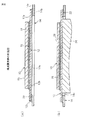
図示のフィルム貼付方法(或いは裏面研削方法)では、まず、第1面10a及びその反対側の第2面10bを有する物体10と、物体10の第1面10aよりも大きな表面12aを有し、可撓性を有するフィルム12と、フィルム12の外周縁12cに沿って配置可能な形状及び寸法を有し、フィルム12よりも高い剛性を有するフレーム部材14と、液状接着剤16とを用意する(図1、図3(a))。
In the illustrated film sticking method (or back surface grinding method), first, an
物体10は、互いに略平行に延びる第1面10a及び第2面10b、並びに第1面10aと第2面10bとの間に延びる環状の外周面10cを有する。物体10は、例えば、第2面10bの全体を研削することによって、最初に与えられた厚みから所望の一様な厚みまで薄肉化されることが期待される平板状要素である。或いは物体10は、第2面10bの研削及びそれによる薄肉化が期待されない平板状要素であってもよい。物体10は、例えば、シリコン、ガリウムヒ素、水晶、サファイヤ、ガラス等からなるウエハや基板であることができる。物体10が円板状の形状を有する場合、物体10の直径は、例えば50mm〜500mmであることができる。
The
図示のフィルム貼付方法を、半導体チップの作製方法における裏面研削工程で実施する場合、物体10は、半導体チップの母材となるウエハであり、第1面10aは、所要の回路パターンが形成された回路面である。この場合、第1面10aは、印刷配線等による多様な凸部11(図4)を有することができる。また、例えば既述の特許文献3に記載されるような「先ダイシング法」を実施する場合には、第1面10aは、厚み方向へ切り込まれた線状の溝(図示せず)を予め所定位置に有することができる。ウエハの厚みは、例えば0.5mm〜1mm程度であり、直径と共に標準化されている。また、裏面研削後の半導体チップの厚みは、例えば50μm〜100μmであり、近年さらなる薄肉化が望まれている。なお、図示の物体10は、ウエハとして一般的な円板状の形状(中心軸線10d(図3(a))を有する)を備えているが、例えばディスプレイ装置の基板のように矩形平板状の形状を備えていてもよい。いずれにしても、物体10の素材、形状、寸法等は特に限定されない。
When the illustrated film sticking method is performed in the back surface grinding step in the semiconductor chip manufacturing method, the
フィルム12は、表面12a及びその反対側の裏面12b、並びに外周縁12cを有する柔軟な膜状要素であり、例えば、樹脂等から全体に一様な厚みに作製される。またフィルム12は、液状接着剤16により物体10の第1面10aに固着されることで第1面10aを保護する機能を有することができる。液状接着剤16として、後述する放射線硬化型の接着剤を使用する場合には、フィルム12は十分な放射線透過性を有することが望ましく、例えば、ポリエチレンテレフタレート等のポリエステル、ポリプロピレン等のポリオレフィン樹脂、ポリ塩化ビニル樹脂、ポリビ塩化ビニリデン樹脂、ポリアミド樹脂等からなるポリマーフィルムであることができる。図示のフィルム貼付方法を、半導体チップの作製方法における裏面研削工程で実施する場合、フィルム12は、物体10の第1面10aであるウエハの回路面を、裏面研削工程やダイシング工程の間、汚損しないように保護し得る物性を有することが望ましい。この場合、フィルム12の厚みは、例えば5μm〜200μmである。
The
フィルム12は、予め適当な形状及び寸法に裁断されたシートとして供給されてもよいし、或いはロールから繰り出して供給され、使用直前に裁断されるものであってもよい。またフィルム12は、物体10に貼付される前に物体10に相似する形状を有するよう予め余剰部分が切断除去されていてもよいし、物体10に貼付された後に物体10に相似する形状になるよう余剰部分が切断除去されてもよい。なお、図示のフィルム12は、物体10の円板形状に相似する円形の形状(中心軸線12d(図3(a))を有する)を備えているが、物体10の第1面10aよりも大きな表面12aを有する点を除いて、フィルム12の素材、形状、寸法等は特に限定されない。
The
フレーム部材14は、第1面14a及びその反対側の第2面14b、並びに第1面14aと第2面14bとの間に延びる内周面14c及びその反対側の外周面14dを有する環状要素であり、例えば、金属、樹脂等から全体に一様な厚みに作製される。フレーム部材14は、第1面14a又は第2面14bがフィルム12の外周縁12cに沿って表面12a又は裏面12bに固定されることで、内縁14cの内側に位置するフィルム12の中央領域を伸展した状態に維持できる剛性を有する。フレーム部材14の剛性は、素材、寸法、形状等によって設定できるが、例えばフィルム12に何らかの張力が加わったときにもフレーム部材14自体に顕著な撓みや変形が生じない程度の剛性であればよい。例えば、フレーム部材14がステンレス鋼製の円環状のものである場合、厚みが約1mm〜2mm程度、内径が約350mm程度、外径が約400mm程度の寸法を有することが、特に直径30mmのシリコンウエハ用として適当である。なお、図示のフレーム部材14は、物体10の円板形状に相似する円環状の形状(中心軸線14e(図3(a))を有する)を備えているが、フィルム12の外周縁12cに沿って配置可能な形状及び寸法を有する点、及びフィルム12よりも高い剛性を有する点を除いて、フレーム部材14の素材、形状、寸法等は特に限定されない。フレーム部材14は、フィルム12と同一の素材から形成されてもよい。
The
液状接着剤16は、硬化又は固化することで物体10の第1面10aにフィルム12の表面12aを強固に固定した状態に保持する接着力を発揮できるものであって、例えば、硬化性接着剤、溶剤系接着剤、ホットメルト型接着剤を含む熱可塑性樹脂、水分散型接着剤等であることができる。ここで、硬化性接着剤は、熱や紫外線等のエネルギー線によって硬化される液状接着剤であり、溶剤系接着剤は、溶剤の蒸発により固化する液状接着剤であり、ホットメルト型接着剤は、加熱により溶融し、冷却により固化される接着剤である。また、水分散型接着剤は水中に接着剤成分が分散したものであって、水の蒸発により、固化する接着剤である。硬化性接着剤としては、エポキシ、ウレタンをベースとする一液熱硬化型接着剤、エポキシ、ウレタン、アクリルをベースとする二液混合反応型接着剤、アクリル、エポキシをベースとする紫外線硬化型、電子線硬化型接着剤が挙げられる。また、溶剤系接着剤としては、ゴム、エラストマー等を溶剤に溶解したゴム系接着剤が挙げられる。なお本願では、狭義の硬化及び固化を「固化」と総称する。
The liquid adhesive 16 can exhibit an adhesive force that holds the
図示のフィルム貼付方法を、半導体チップの作製方法における裏面研削工程で実施する場合、液状接着剤16は、固化する前に、物体(ウエハ)10の第1面(回路面)10aに形成される凸部11間の隙間や「先ダイシング法」のための線状の溝を満遍無く円滑に充填し、気泡の混入が無い接合層18(図3(b))を物体(ウエハ)10とフィルム12との間に形成し得る物性を有することが望ましい。特に、接合層18の厚みを均一にするために、液状接着剤16は、作業環境(例えば25℃)下での固化前の粘度が10Pa・s(10000cP)未満であることが望ましい。なお粘度は、25℃環境下でB型回転粘度計(ロータ形状と回転数に応じて(粘度)=(指示値)×(換算乗数)で換算する)により測定された値である。より具体的には、粘度は、25℃環境下でロータ形状No.2、回転数12rpmのブルックフィールド型粘度計(BM)(例えば協和科学株式会社(東京)のRVDV−E等)により測定される。
When the illustrated film sticking method is performed in the back grinding process in the semiconductor chip manufacturing method, the
また液状接着剤16は、溶剤系接着剤では溶媒除去後、硬化型接着剤では硬化後、ホットメルト系接着剤では常温固化後の使用環境下(例えば25℃)で、100MPa以上の貯蔵弾性率を有し、かつ、裏面研削工程中に到達しうる温度(例えば50℃)で、10MPa以上の貯蔵弾性率を有することが好ましい。液状接着剤16がこのような貯蔵弾性率を有することにより、物体10の裏面研削工程中に液状接着剤16が応力により歪むことが防止され、物体10の第2面10bを均一に研削することができる。なお貯蔵弾性率は、温度上昇モード(Temp Ramp Mode)、引張モード、周波数1Hz、歪み(Strain)0.04%、昇温速度5℃/分の条件で、サンプルサイズ22.7mm×10mm×50μmの接着剤に対して測定した値である。このような貯蔵弾性率は、レオメトリックス社製「SOLIDS ANALYZER RSA II」(商品名)を使用して測定できる。
The
さらに、裏面研削工程中に接合層18に水が浸入したりダイシング工程中にチッピング(エッジ欠け)が生じたりすることを防止するために、液状接着剤16の固化時の接着力は、例えば0.1N/25mm〜0.5N/25mm、好ましくは0.1N/25mm〜0.2N/25mmであることができる。なお接着力は、JIS Z 0237に準拠した方法で測定される(すなわち、幅25mmの試験片を、2.0Kgのゴムローラを毎秒5mmの速さで一往復させて、被着体(SUS430BA板)に圧着し、圧着後20分〜40分の時点で、引張試験機により毎分300±30mmの速さで試験片を被着体から180°方向へ引き剥がす。)。液状接着剤16の固化後の接合層18の厚みは、特に限定されないが、物体10の第1面10aの凹凸等を吸収してフィルム12を平坦化できる範囲であることが望ましく、例えば10μm〜150μmであり、好ましくは20μm〜100μmである。
Further, in order to prevent water from entering the
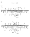
上記した構成要素群に対し、図示のフィルム貼付方法(或いは裏面研削方法)の次ステップでは、物体10の第1面10a又はフィルム12の表面12aに液状接着剤16を配置する。液状接着剤16は、適当な装置により物体10の第1面10a又はフィルム12の表面12aに滴下したり塗布したりすることで配置できる。図示構成では、物体10がその第1面10aを上に向けてテーブル20の上に搭載され(図4(a))、物体10の第1面10aの、中心軸線10dを含む領域に、十分な量の液状接着剤16が配置されている(図4(b))。なお、物体10の第1面10aに液状接着剤16を配置する場合には、例えば、物体10をその中心軸線10dの周りで回転させたり、或いは物体10を振動させたりすることで、第1面10aの全体に液状接着剤16を行き渡らせることもできる。
In the next step of the illustrated film sticking method (or back surface grinding method) for the above-described component group, the
他方、フィルム12の外周縁12cに沿って、フレーム部材14を固定する(図3(b))。図ではフレーム部材14は、フィルム12の表面12aの、外周縁12cの全周に沿った環状の領域に、一様に固定されている。フレーム部材14の固定は、接着剤、両面粘着テープ、融着等の種々の接合手段により行うことができる。図示構成では、接合手段として液状接着剤16と同様の液状接着剤が用いられ、液状接着剤が固化した接合層22(図3(b))により、フレーム部材14の第2面14bがフィルム12の表面12aに強固に固定されている。このような液状接着剤は、フィルム12の表面12aの外周縁12cに沿った環状領域、又はフレーム部材14の第2面14bに、適当なノズルを用いて線状に連続させて配置することができる。このとき、フィルム12又はフレーム部材14を中心軸線12d又は14eの周りで回転させながら静止ノズルにより液状接着剤を配置したり、静止したフィルム12又はフレーム部材14に対しロボット等の自動機械を用いてノズルを円形軌道に沿って移動させながら液状接着剤を配置したりすることができる。
On the other hand, the
次に、物体10とフィルム12とを、第1面10aと表面12aとが互いに対向するとともにフィルム12の外周縁12cに沿った領域(したがってフレーム部材14)が物体10の外側に張り出す相対位置に配置して、第1面10aと表面12aとの双方を液状接着剤16に接触させる(図4(c))。そして、物体10の第1面10aとフィルム12の表面12aとの間に、液状接着剤16を十分に行き渡らせる(図4(d)、(e))。このとき、フィルム12の外周縁12cに沿ってフレーム部材14が一様に固定されているので、フレーム部材14の内側に位置するフィルム12の中央領域12e(図3(b))をフレーム部材14によって伸展した状態(つまり撓みの無い状態)に維持することができ、物体10の第1面10aとフィルム12の表面12aとを互いに略平行な配置で液状接着剤16に接触させることができる。
Next, relative positions of the
最後に、液状接着剤16を固化させて、物体10の第1面10aにフィルム12を固着させる(図4(f))。例えば液状接着剤16が紫外線硬化型の接着剤である場合、図示のように、フィルム12の裏面12b側から紫外線Rを照射して、液状接着剤16を固化させる。液状接着剤16が前述した物性を有することにより、液状接着剤16は、物体10の第1面10aに形成される凸部11間の隙間や「先ダイシング法」のための線状の溝(図示せず)を満遍無く円滑に充填し、気泡の混入が無い接合層18(図3(b))を物体10とフィルム12との間に形成することができる。接合層18は、物体10の第1面10aの全体にフィルム12の表面12aを強固に接合し、以て、物体10がフィルム12を安定して支持すること、或いはフィルム12が物体10を安定して支持することを可能にする。なお図示構成では、液状接着剤16が固化した状態で、物体10、フィルム12及びフレーム部材14は互いに略同軸に配置され、物体10の外周面10cとフレーム部材14の内周面14cとの間に、全体に略均一な寸法の環状の間隙が形成されている(図2、図3(b))。
Finally, the
上記構成において、フィルム12へのフレーム部材14の固定ステップは、物体10の第1面10aとフィルム12の表面12aとの双方を液状接着剤16に接触させる前に行ってもよいし、物体10の第1面10aとフィルム12の表面12aとの双方を液状接着剤16に接触させると同時又はその後に行ってもよい。特に、液状接着剤16と同様の液状接着剤を用いてフレーム部材14をフィルム12に固定する構成では、例えばフィルム12の表面12aの全体に液状接着剤16を塗布等により配置し、物体10の第1面10aとフィルム12の表面12aとの双方を液状接着剤16に接触させると同時に又は前後して、フレーム部材14の第2面14bを液状接着剤16に接触させ、その状態で液状接着剤16の全体を固化させることにより、接合層18、22を形成して物体10とフレーム部材14との双方にフィルム12を固着させることができる。なおこの場合、少なくとも、物体10、フィルム12及びフレーム部材14を液状接着剤16に接触させるステップ及びその状態で液状接着剤16を固化させるステップを、真空環境で行うことが望ましい。また、これらステップを含む全てのステップを、真空環境で行うこともできる。
In the above configuration, the fixing step of the
上記構成を有するフィルム貼付方法では、フィルム12の外周縁12cに沿って、フィルム12よりも高い剛性を有するフレーム部材14を固定したから、フレーム部材14の内側に位置するフィルム12の中央領域12eを撓みの無い状態に維持することができる。それにより、物体10の第1面10aとフィルム12の表面12aとを互いに略平行に配置して、液状接着剤16に接触させることができる。また、物体10とフィルム12との接合手段として液状接着剤16を用いたから、物体10の第1面10aの様々な凹凸を液状接着剤16により吸収して、液状接着剤16が固化した後のフィルム12の平坦性を確保することができるとともに、気泡の混入が無い接合層18を物体10とフィルム12との間に形成することができる。そのような接合層18は、強固な接着力を長期間に渡り安定して維持できるものである。したがって、上記フィルム貼付方法によれば、簡易な手法で正確にフィルム12を物体10に貼付できる。
In the film sticking method having the above configuration, since the
上記フィルム貼付方法によって第1面10aにフィルム12を固着させた物体10に対し、図示の裏面研削方法では、物体10及びフィルム12をフレーム部材14と共にテーブル20から取り上げて、上下を反転させ、物体10の第2面10bを上に向けた状態(図3(b))で、別の静止台24に載置する。そして、例えば真空吸着等の保持手段を用いて、フレーム部材14の内側で物体10及びフィルム12を静止台24上に固定的に支持する。このとき、フレーム部材14からフィルム12に加わる不要な応力を排除してフィルム12を平坦な形態に維持できるように、物体10及びフィルム12に対してフレーム部材14を固定した状態に保持することもできる。この状態で、物体10の第2面10bの全体を研削装置(図示せず)により研削し、平坦な加工面26を形成する(図3(c))。
In the illustrated backside grinding method, the
上記構成を有する裏面研削方法では、物体10の第1面10aをフィルム12によって保護するようにしたから、保護のためにガラス板を用いる方法に比べて、コストを削減することができる。また、フィルム12の外周縁12cに沿って、フィルム12よりも高い剛性を有するフレーム部材14を固定したから、フレーム部材14の内側に位置するフィルム12の中央領域12eを撓みの無い状態に維持し、物体10の第1面10aとフィルム12の表面12aとを互いに略平行な配置で液状接着剤16に接触させることができる。しかも、物体10の第2面10bを研削するための段取り作業(例えば上下の反転、静止台24への搭載等)が、フレーム部材14をハンドリングすることで迅速に実施できるようになる。
In the back surface grinding method having the above-described configuration, the
さらに、物体10とフィルム12との接合手段として液状接着剤16を用いたから、液状接着剤16が固化した後のフィルム12の平坦性を確保することができるとともに、気泡の混入が無い接合層18を物体10とフィルム12との間に形成することができる。フィルム12の平坦性及び物体10の第1面10aとフィルム12の表面12aとの平行度を確保することで、物体10の第2面10bを均一に研削して平坦な加工面26を形成でき、物体10の厚みを数十μmオーダまで一様に削減することができる。また、気泡の混入が無い接合層18は、強固な接着力を長期間に渡り安定して維持できるとともに、研削工程中に加工液が接合層18の内部に浸入することを防止できる効果を奏する。したがって、上記裏面研削方法によれば、簡易な手法で正確に物体10の厚みを削減できる。
Further, since the
本発明の一実施形態による半導体チップの作製方法は、上記フィルム貼付方法を含む上記裏面研削方法を、回路面の反対側の裏面を研削してウエハの厚みを一様に削減する裏面研削工程として実施するものである。この半導体チップ作製方法では、裏面研削工程により、ウエハ(すなわち物体10)の回路面(すなわち第1面10a)の反対側の裏面(すなわち第2面10b)を研削して加工面26を形成する。そして、加工面26を形成したウエハ(物体10)に対し、予め定めた切削線に沿って加工面26を切削(ダイシング)して、ウエハ(物体10)を複数のチップ(図示せず)に分断する。このとき、加工面26を形成したウエハ(物体10)を静止台24の上に載置したままの状態で、接合層18が発揮するウエハ(物体10)とフィルム12との強固な接着力の下に、切削工程を正確に実施できる。したがって、この半導体チップ作製方法によれば、裏面研削によるウエハの厚みの削減及び切削による複数のチップへの分断を、簡易な手法で正確に実施できる。
According to an embodiment of the present invention, there is provided a method for manufacturing a semiconductor chip, wherein the back surface grinding method including the film pasting method is a back surface grinding step for uniformly reducing a wafer thickness by grinding a back surface opposite to a circuit surface. To implement. In this semiconductor chip manufacturing method, the processed
また、本発明の他の実施形態による半導体チップの作製方法として、既述の特許文献3に記載されるような先ダイシング法を採用することもできる。この構成では、ウエハ(すなわち物体10)の回路面(すなわち第1面10a)の所定位置(上記ダイシング工程における切削位置)に、厚み方向へ切り込まれた線状の溝が予め形成される。したがって、上記した裏面研削工程により、ウエハ(物体10)の回路面(第1面10a)の反対側の裏面(すなわち第2面10b)を研削して加工面26を形成することで、ウエハ(物体10)を複数のチップ(図示せず)に分断することができる。なお、ウエハ(物体10)のダイシング工程及び先ダイシング法の詳細は、後述する。
In addition, as a method of manufacturing a semiconductor chip according to another embodiment of the present invention, a tip dicing method as described in
上記したフィルム貼付方法(或いは裏面研削方法、半導体チップ作製方法)において、フィルム12の外周縁12cに沿ってフレーム部材14を固定する際には、図5に示すように、フィルム12に径方向外方への一様な張力を加えて、特に中央領域12eをピンと張った状態で、フレーム部材14を固定することができる(図5(a)、(b))。この構成では、張力を加えたフィルム12に対し、液状接着剤16と同様の液状接着剤を用いてフレーム部材14を貼着し、フィルム12に張力を加えたままの状態で液状接着剤を固化させて、形成された接合層22により、フレーム部材14の第2面14bをフィルム12の表面12aに強固に固定することが望ましい。この場合、フィルム12は、フレーム部材14を貼着する前にフレーム部材14に相似する形状を有するよう予め余剰部分が切断除去されていてもよいし、フレーム部材14を貼着した後にフレーム部材14に相似する形状になるよう余剰部分が切断除去されてもよい。なお、フィルム12に加える張力は、フィルム12の撓みを確実に除去できる大きさであることが好ましく、例えば10g/cm〜1000g/cmである。フレーム部材14は、このような張力を加えたフィルム12を、張力が加わったままの状態に保持できる剛性を有すればよい。
When the
この構成によれば、フレーム部材14の内周面14cの内側に位置するフィルム12の中央領域12eを、長期間に渡り、フレーム部材14によって撓みを排除した状態に確実に維持することができる(図5(c))。したがって、フィルム貼付工程、裏面研削工程、ダイシング工程を、一層正確に実施できる。
According to this structure, the center area |
上記したフィルム貼付方法(或いは裏面研削方法、半導体チップ作製方法)において、フィルム12の外周縁12cに沿ってフレーム部材14を固定する際には、図6に示すように、フィルム12の裏面12bにフレーム部材14を固定することができる(図6(a))。図ではフレーム部材14は、フィルム12の裏面12bの、外周縁12cの全周に沿った環状の領域に、一様に固定されている。フレーム部材14の固定は、接着剤、両面粘着テープ、融着等の種々の接合手段により行うことができる。図示構成では、接合手段として液状接着剤16と同様の液状接着剤が用いられ、液状接着剤が固化した接合層22により、フレーム部材14の第1面14aがフィルム12の裏面12bに強固に固定されている。このような液状接着剤の使用の詳細は、フレーム部材14をフィルム12の表面12aに固定する前述した構成におけるものと同様である。
When the
この構成によっても、フレーム部材14をフィルム12の表面12aに固定する前述した構成と同様に、フレーム部材14の内周面14cの内側に位置するフィルム12の中央領域12eを、フレーム部材14によって撓みを排除した状態に維持できるから、簡易な手法で正確にフィルム12を物体10に貼付できる。特にこの構成によれば、裏面研削工程やダイシング工程に際し、物体10の第2面10bを上に向けた状態でフィルム12の中央領域12eを静止台24に固定的に載置する(図6(b))ことで、フレーム部材14の存在が研削装置やダイシング装置の円滑な操作を妨げる懸念を排除できる。また、物体10の研削屑が、物体10とフレーム部材14との間の環状の間隙に保留されてしまうことを回避できる。したがって、裏面研削工程、ダイシング工程を、一層正確に実施できる。
Also with this configuration, the
上記したフィルム貼付方法(或いは裏面研削方法、半導体チップ作製方法)においては、液状接着剤16を固化させるステップの前に、第1面10aと表面12aとの双方を液状接着剤16に接触させた状態で物体10とフィルム12とを回転させて、第1面10aと表面12aとの間に液状接着剤16を行き渡らせるようにすることができる(図4(d))。この場合、遠心力により余剰の液状接着剤16が除去されて、フィルム12の表面12aが物体10の第1面10aの凸部11に実質的に接触したときに、物体10及びフィルム12の回転を停止することができる(図4(e))。例えばスピンコート工程と称するこのような手法によれば、物体10の第1面10aが多様な凹凸を有する場合であっても、液状接着剤16を物体10の第1面10aとフィルム12の表面12aとの間の隙間の隅々に配置でき、以て、液状接着剤16の固化後に、気泡の混入が無い接合層18を確実に形成することができる(図4(f))。
In the film sticking method (or back grinding method, semiconductor chip manufacturing method) described above, both the
上記スピンコート工程において、物体10とフィルム12とを回転させる際には、図7(a)に示すように、第1面10aと表面12aとの双方を液状接着剤16に接触させた状態で、フレーム部材14を物体10に対して固定的に支持しながら物体10とフィルム12とを同軸配置で回転させることができる。この構成によれば、回転中に生じ得る物体10に対するフィルム12の浮き上がりや中心軸線10d、12d同士の位置ずれを、フレーム部材14を固定的に支持することにより防止できる。その結果、液状接着剤16が固化した後に、フィルム12の平坦性及び物体10の第1面10aとフィルム12の表面12aとの平行度を、高水準に確保することができる。
In the spin coating step, when the
図7(a)に示す構成に加えて、又はその代わりに、図7(b)に示すように、第1面10aと表面12aとの双方を液状接着剤16に接触させた状態で、フィルム12を物体10に対して固定的に支持しながら物体10とフィルム12とを同軸配置で回転させることもできる。この構成によっても、回転中に生じ得る物体10に対するフィルム12の浮き上がりや中心軸線10d、12d同士の位置ずれを、フィルム12を固定的に支持することにより防止できる。その結果、液状接着剤16が固化した後に、フィルム12の平坦性及び物体10の第1面10aとフィルム12の表面12aとの平行度を、高水準に確保することができる。
In addition to or instead of the configuration shown in FIG. 7A, as shown in FIG. 7B, the film is formed with both the
図7(a)に示すスピンコート工程を実施するための、本発明の一実施形態によるフィルム貼付装置は、物体10の第1面10aとフィルム12の表面12aとの双方を液状接着剤16に接触させた状態で、フレーム部材14を物体10に対して固定的に支持するフレーム支持部28と、フレーム支持部28がフレーム部材14を物体10に対して固定的に支持した状態で、物体10とフィルム12とを同軸配置で回転させる駆動部(テーブル20及びフレーム支持部28の回転駆動機構(図示せず))とを備える。フレーム支持部28は、テーブル20に固定的に搭載した物体10に対し、フィルム12の外周縁12cに沿って固定したフレーム部材14を、それぞれの中心軸線10d、12d、14eが合致する同軸配置で固定的に支持できる支持台30を有する。支持台30は、フレーム部材14がそれ自体に歪みを有していた場合に、そのような歪みを補正する機構を有することができる。
A film sticking apparatus according to an embodiment of the present invention for performing the spin coating process shown in FIG. 7A is a liquid adhesive 16 on both the
フレーム支持部28はまた、支持台30の径方向内側に、物体10とフィルム12との間から遠心力により放出される余剰の液状接着剤16を受け取る環状の壁部32を有することができる。壁部32によって受け取られた余剰の液状接着剤16は、図示しない回収機構によって回収され、例えば再使用される。壁部32は、フレーム部材14を支持台30に支持した状態で、図示のようにフィルム12の中央領域12eを裏面12bが凸になるように僅かに持ち上げる形状を有することができる。この構成によれば、フレーム部材14がそれ自体に歪みを有していた場合にも、そのような歪みの影響を受けることなく、物体10の第1面10aとフィルム12の表面12aとを互いに略平行な配置で液状接着剤16に接触させることができる。なお、図示構成では、物体10がその第1面10aを上に向けてテーブル20の上に搭載されているが、物体10とフィルム12との上下関係を逆にすることもできる。
The
フレーム支持部28は、テーブル20に一体的に連結されていてもよいし、テーブル20から機能的に分離されていてもよい。フレーム支持部28がテーブル20に一体的に連結されている場合、物体10とフィルム12とは、フレーム部材14を介して同期して回転する。物体10とフィルム12とが同期して回転することにより、物体10との間に液状接着剤16を介在させたフィルム12の平坦性を向上させることができる場合がある。また、フレーム支持部28がテーブル20から機能的に分離されている場合、物体10とフレーム部材14(したがってフィルム12)とを、意図的に同期させずに回転させることもできる。物体10とフィルム12とが異なる回転数で回転することにより、物体10との間に液状接着剤16を介在させたフィルム12の平坦性を向上させることができる場合がある。図示のフィルム貼付装置はさらに、テーブル20と支持台30との相対位置関係(したがって物体10とフィルム12との相対位置関係)を微調整する機構や、予め物体10の第1面10aの全体に液状接着剤16を行き渡らせるべくテーブル20を振動させる機構等を、備えることもできる。
The
図7(b)に示すスピンコート工程を実施するための、本発明の他の実施形態によるフィルム貼付装置は、上記したフレーム支持部28に加えて、或いはその代わりに、物体10の第1面10aとフィルム12の表面12aとの双方を液状接着剤16に接触させた状態で、フィルム12を物体10に対して固定的に支持するフィルム支持部34と、フィルム支持部34がフィルム12を物体10に対して固定的に支持した状態で、物体10とフィルム12とを同軸配置で回転させる駆動部(テーブル20及びフィルム支持部34の回転駆動機構(図示せず))とを備える。フィルム支持部34は、テーブル20に固定的に搭載した物体10に対し、フィルム12を、それぞれの中心軸線10d、12dが合致する同軸配置で固定的に支持できる支持台36を有する。支持台36は、例えば真空吸着や粘着により、フィルム12の中央領域12eをその裏面12bから支持することができる。
The film sticking apparatus according to another embodiment of the present invention for performing the spin coating process shown in FIG. 7B is the first surface of the
フィルム支持部34は、支持台36にフィルム12を支持した状態で、フィルム12から物体10に自重等による圧力が加わらないようにしたり、フィルム12から物体10に意図的に圧力を加えたり、フィルム12を物体10から離れる方向へ引き上げたりするように構成できる。いずれの構成によっても、物体10との間に液状接着剤16を介在させたフィルム12の平坦性を向上させることができる場合がある。また、フィルム支持部34は、テーブル20と同期して回転したり、或いは意図的にテーブル20と同期せずに回転したりするように構成できる。いずれの構成によっても、物体10との間に液状接着剤16を介在させたフィルム12の平坦性を向上させることができる場合がある。
The
図8を参照して、本発明のさらに他の実施形態によるフィルム貼付方法、裏面研削方法及び半導体チップ作製方法を説明する。なお図示の方法は、第1面10aと表面12aとの双方を液状接着剤16に接触させた状態で物体10とフィルム12とを回転させるスピンコート工程を行わない点を除いて、図3及び図4を参照して説明した方法と同様の構成を有する。したがって、対応する構成の説明は適宜省略する。
With reference to FIG. 8, a film sticking method, a back surface grinding method, and a semiconductor chip manufacturing method according to still another embodiment of the present invention will be described. 3A and 3B, except that the spin coating process is not performed in which the
まず、第1面10a及びその反対側の第2面10bを有する物体10と、物体10の第1面10aよりも大きな表面12aを有し、可撓性を有するフィルム12と、フィルム12の外周縁12cに沿って配置可能な形状及び寸法を有し、フィルム12よりも高い剛性を有するフレーム部材14と、液状接着剤16とを用意する(図1)。次に、物体10をその第1面10aを上に向けてテーブル20の上に搭載し(図8(a))、物体10の第1面10aの中心軸線10dを含む領域に液状接着剤16を配置する(図8(b))。その状態で、物体10をその中心軸線10dの周りで回転させて、第1面10aの全体に液状接着剤16を行き渡らせる(図8(c))。
First, the
他方、フィルム12の外周縁12cに沿って、フレーム部材14を固定する。そして、物体10とフィルム12とを、第1面10aと表面12aとが互いに対向するとともにフィルム12の外周縁12cに沿った領域(したがってフレーム部材14)が物体10の外側に張り出す相対位置に配置して、第1面10aと表面12aとの双方を液状接着剤16に接触させる(図8(d))。このとき、フィルム12の外周縁12cに沿ってフレーム部材14が一様に固定されているので、フレーム部材14の内側に位置するフィルム12の中央領域12eをフレーム部材14によって伸展した状態(つまり撓みの無い状態)に維持することができ、物体10の第1面10aとフィルム12の表面12aとを互いに略平行な配置で液状接着剤16に接触させることができる。
On the other hand, the
次に、液状接着剤16を固化させて、物体10の第1面10aにフィルム12を固着させる(図8(e))。液状接着剤16が前述した物性を有することにより、液状接着剤16は、物体10の第1面10aに形成される凸部11間の隙間を満遍無く円滑に充填し、気泡の混入が無い接合層18を物体10とフィルム12との間に形成することができる。これにより、フィルム貼付工程(フィルム貼付方法)が完了する。なお、上記したフィルム貼付工程は、少なくとも、物体10及びフィルム12を液状接着剤16に接触させるステップ及びその状態で液状接着剤16を固化させるステップを、真空環境で行うことが望ましい。また、これらステップを含む全てのステップを、真空環境で行うこともできる。
Next, the
上記フィルム貼付工程によって第1面10aにフィルム12を固着させた物体10に対し、図示の裏面研削方法では、物体10及びフィルム12をフレーム部材14と共にテーブル20から取り上げて、上下を反転させ、物体10の第2面10bを上に向けた状態で別の静止台等に載置する。そして、例えば真空吸着等の保持手段を用いて、フレーム部材14の内側で物体10及びフィルム12を固定的に支持するとともに、物体10及びフィルム12に対してフレーム部材14を固定した状態に保持する。この状態で、物体10の第2面10bの全体を研削装置(図示せず)により研削し、平坦な加工面26を形成する(図8(f))。これにより、裏面研削工程(裏面研削方法)が完了する。
In the illustrated backside grinding method, the
図示の半導体チップ作製方法は、上記フィルム貼付工程を含む上記裏面研削工程を、回路面の反対側の裏面を研削してウエハの厚みを一様に削減するために実施するものである。この半導体チップ作製方法では、裏面研削工程により、回路面(第1面10a)の反対側の裏面(第2面10b)を研削して加工面26を形成したウエハ(物体10)に対し、予め定めた切削線38に沿って加工面26を切削(ダイシング)して、ウエハ(物体10)を複数のチップ40に分断する(図8(g))。分断した個々のチップ40は、例えばフィルム12の裏面12bから図示しないピン等で突き上げて、接合層18とチップ40の表面との界面に剥離を生じさせることにより、フィルム12から1つずつ取り上げることができる。なお、切削線38は通常、ウエハ(物体10)の回路面(第1面10a)に予め設けられており、加工面26側から切削線38を視認することは一般に困難である。そこで、上記したダイシング工程においては、例えば既述の特許文献2に記載されるような、画像認識機能を有するダイシング装置を用いることにより、回路面(第1面10a)側の切削線38を画像上で認識しながら、加工面26を正確に切削(ダイシング)することができる。
In the illustrated semiconductor chip manufacturing method, the back surface grinding step including the film pasting step is performed in order to uniformly reduce the thickness of the wafer by grinding the back surface opposite to the circuit surface. In this semiconductor chip manufacturing method, the back surface (
上記構成を有する図8の実施形態によるフィルム貼付方法、裏面研削方法及び半導体チップ作製方法は、図3及び図4を参照して説明したフィルム貼付方法、裏面研削方法及び半導体チップ作製方法と同等の効果を奏するものである。 The film sticking method, back grinding method, and semiconductor chip manufacturing method according to the embodiment of FIG. 8 having the above-described configuration are equivalent to the film sticking method, back grinding method, and semiconductor chip manufacturing method described with reference to FIGS. There is an effect.
図9を参照して、本発明のさらに他の実施形態によるフィルム貼付方法、裏面研削方法及び半導体チップ作製方法を説明する。なお図示の方法は、第1面10aと表面12aとの双方を液状接着剤16に接触させた状態で物体10とフィルム12とを回転させるスピンコート工程を行わない点を除いて、図3及び図4を参照して説明した方法と同様の構成を有する。したがって、対応する構成の説明は適宜省略する。
With reference to FIG. 9, the film sticking method, back surface grinding method, and semiconductor chip preparation method by further another embodiment of this invention are demonstrated. 3A and 3B, except that the spin coating process is not performed in which the
まず、第1面10a及びその反対側の第2面10bを有する物体10と、物体10の第1面10aよりも大きな表面12aを有し、可撓性を有するフィルム12と、フィルム12の外周縁12cに沿って配置可能な形状及び寸法を有し、フィルム12よりも高い剛性を有するフレーム部材14と、液状接着剤16とを用意する(図1)。ここで、物体10は、第1面10aに、厚み方向へ切り込まれた線状の溝42を予め所定位置に有している。次に、物体10をその第1面10aを上に向けてテーブル20の上に搭載し(図9(a))、物体10の第1面10aの中心軸線10dを含む領域に液状接着剤16を配置する(図9(b))。その状態で、物体10をその中心軸線10dの周りで回転させて、第1面10aの全体に液状接着剤16を行き渡らせる(図9(c))。
First, the
他方、フィルム12の外周縁12cに沿って、フレーム部材14を固定する。そして、物体10とフィルム12とを、第1面10aと表面12aとが互いに対向するとともにフィルム12の外周縁12cに沿った領域(したがってフレーム部材14)が物体10の外側に張り出す相対位置に配置して、第1面10aと表面12aとの双方を液状接着剤16に接触させる(図9(d))。このとき、フィルム12の外周縁12cに沿ってフレーム部材14が一様に固定されているので、フレーム部材14の内側に位置するフィルム12の中央領域12eをフレーム部材14によって伸展した状態(つまり撓みの無い状態)に維持することができ、物体10の第1面10aとフィルム12の表面12aとを互いに略平行な配置で液状接着剤16に接触させることができる。
On the other hand, the
次に、液状接着剤16を固化させて、物体10の第1面10aにフィルム12を固着させる(図9(e))。液状接着剤16が前述した物性を有することにより、液状接着剤16は、物体10の第1面10aに形成される凸部11間の隙間や線状の溝42を満遍無く円滑に充填し、気泡の混入が無い接合層18を物体10とフィルム12との間に形成することができる。これにより、フィルム貼付工程(フィルム貼付方法)が完了する。なお、上記したフィルム貼付工程は、少なくとも、物体10及びフィルム12を液状接着剤16に接触させるステップ及びその状態で液状接着剤16を固化させるステップを、真空環境で行うことが望ましい。また、これらステップを含む全てのステップを、真空環境で行うこともできる。
Next, the
上記フィルム貼付工程によって第1面10aにフィルム12を固着させた物体10に対し、図示の裏面研削方法では、物体10及びフィルム12をフレーム部材14と共にテーブル20から取り上げて、上下を反転させ、物体10の第2面10bを上に向けた状態で別の静止台等に載置する。そして、例えば真空吸着等の保持手段を用いて、フレーム部材14の内側で物体10及びフィルム12を固定的に支持するとともに、物体10及びフィルム12に対してフレーム部材14を固定した状態に保持する。この状態で、物体10の第2面10bの全体を研削装置(図示せず)により研削し、平坦な加工面26を形成する(図9(f))。これにより、裏面研削工程(裏面研削方法)が完了する。
In the illustrated backside grinding method, the
図示の半導体チップ作製方法は、上記フィルム貼付工程を含む上記裏面研削工程を、回路面の反対側の裏面を研削してウエハの厚みを一様に削減するために実施するものである。この半導体チップ作製方法では、裏面研削工程により、ウエハ(物体10)の回路面(第1面10a)の反対側の裏面(第2面10b)を、予めウエハ(物体10)の回路面(第1面10a)に設けた線状の溝42に達するまで研削して加工面26を形成する。それにより、ウエハ(物体10)を複数のチップ40に分断することができる(図9(f))。分断した個々のチップ40は、例えばフィルム12の裏面12bから図示しないピン等で突き上げて、接合層18とチップ40の表面との界面に剥離を生じさせることにより、フィルム12から1つずつ取り上げることができる。
In the illustrated semiconductor chip manufacturing method, the back surface grinding step including the film pasting step is performed in order to uniformly reduce the thickness of the wafer by grinding the back surface opposite to the circuit surface. In this semiconductor chip manufacturing method, the back surface (
上記構成を有する図9の実施形態によるフィルム貼付方法、裏面研削方法及び半導体チップ作製方法は、図3及び図4を参照して説明したフィルム貼付方法、裏面研削方法及び半導体チップ作製方法と同等の効果を奏するものである。 The film sticking method, back grinding method and semiconductor chip manufacturing method according to the embodiment of FIG. 9 having the above-described configuration are equivalent to the film sticking method, back grinding method and semiconductor chip manufacturing method described with reference to FIGS. There is an effect.
図8及び図9に示すフィルム貼付方法、裏面研削方法及び半導体チップ作製方法において、物体10の第1面10aに液状接着剤16を配置した状態で物体10を回転させて、第1面10aの全体に液状接着剤16を行き渡らせるステップ(図8(c)、図9(c))は、物体10を回転させる代わりに、或いはそれに加えて、物体10を振動させることにより第1面10aに液状接着剤16を行き渡らせるようにすることもできる。図10は、物体10にそのような振動を加えることができる接着剤配置装置の一例を示す。
In the film sticking method, the back surface grinding method, and the semiconductor chip manufacturing method shown in FIGS. 8 and 9, the
図示の接着剤配置装置は、物体10を固定的に搭載できるテーブル44と、テーブル44に連結される原動機46とを備える。原動機46の回転出力軸48には、物体10の中心軸線10dと同軸で回転する偏心錘50が装着される。テーブル44及び原動機46は、ばね52を介して静止機台54に支持される。原動機46が始動すると、偏心錘50が偏心回転運動を生じ、それに伴い、テーブル44及び原動機46が振動して、テーブル44に搭載した物体10を振動させる。このような回転運動による振動を物体10に加えることにより、物体10の第1面10aの全体に液状接着剤16を迅速に行き渡らせることができる。
The illustrated adhesive placement device includes a table 44 on which the
本発明のさらに他の態様として、フレーム部材14を使用しない実施形態によるフィルム貼付方法を、図11を参照して説明する。このフィルム貼付方法は、フレーム部材14を使用しない点を除いて、図3及び図4並びに図7(b)を参照して説明した方法と同様の構成を有する。したがって、対応する構成の説明は適宜省略する。
As still another aspect of the present invention, a film sticking method according to an embodiment that does not use the
このフィルム貼付方法では、まず、第1面10a及びその反対側の第2面10bを有する物体10と、可撓性を有するフィルム12と、液状接着剤16とを用意する。次に、物体10をその第1面10aを上に向けてテーブル20の上に搭載し、物体10とフィルム12とを、第1面10aと表面12aとが互いに対向する相対位置に配置して、第1面10aと表面12aとの双方を液状接着剤16に接触させる。この状態で、フィルム支持部34によりフィルム12を物体10に対して固定的に支持しながら、物体10とフィルム12とを同軸配置で回転させて、第1面10aと表面12aとの間に液状接着剤16を行き渡らせる。最後に、液状接着剤16を固化させて、物体10の第1面10aにフィルム12を固着させる。
In this film sticking method, first, an
図11に示すフィルム貼付方法では、図7(b)に示す方法と同様に、フィルム支持部34は、支持台36にフィルム12を支持した状態で、フィルム12から物体10に自重等による圧力が加わらないようにしたり、フィルム12から物体10に意図的に圧力を加えたり、フィルム12を物体10から離れる方向へ引き上げたりするように構成できる。また、フィルム支持部34は、テーブル20と同期して回転したり、或いは意図的にテーブル20と同期せずに回転したりするように構成できる。さらに、図7(b)に示すフレーム支持部28を用いないので、フィルム支持部34は、テーブル20によって回転する物体10の回転運動が、液状接着剤16の粘性によりフィルム12に伝達され、その結果として連れ回りするように構成することもできる。いずれの構成によっても、物体10との間に液状接着剤16を介在させたフィルム12の平坦性を向上させることができる場合がある。
In the film affixing method shown in FIG. 11, as in the method shown in FIG. 7B, the
上記構成を有する図11の実施形態によるフィルム貼付方法は、図3及び図4を参照して説明したフィルム貼付方法と同等の効果を奏するものである。なお、上記フィルム貼付方法においても、物体10の第1面10aとフィルム12の表面12aとの双方を液状接着剤16に接触させる前に、図10に示す接着剤配置装置を用いて、物体10を振動させて第1面10aの全体に液状接着剤16を行き渡らせるようにすることができる。
The film sticking method according to the embodiment of FIG. 11 having the above configuration has the same effect as the film sticking method described with reference to FIGS. 3 and 4. Also in the above-described film sticking method, before the
10 物体(ウエハ)
10a 第1面(回路面)
10b 第2面(裏面)
12 フィルム
12a 表面
12b 裏面
14 フレーム部材
16 液状接着剤
18、22 接合層
20 テーブル
26 加工面
28 フレーム支持部
34 フィルム支持部
40 チップ
10 Object (wafer)
10a 1st surface (circuit surface)
10b Second side (back side)
DESCRIPTION OF
Claims (17)
第1面及び該第1面の反対側の第2面を有する物体と、該物体の該第1面よりも大きな表面を有し、可撓性を有するフィルムと、該フィルムの外周縁に沿って配置可能な形状及び寸法を有し、該フィルムよりも高い剛性を有するフレーム部材と、液状接着剤とを用意するステップと、
前記物体の前記第1面又は前記フィルムの前記表面に前記液状接着剤を配置するステップと、
前記フィルムの前記外周縁に沿って前記フレーム部材を固定するステップと、
前記物体と前記フィルムとを、前記第1面と前記表面とが互いに対向するとともに前記フィルムの前記外周縁に沿った領域が前記物体の外側に張り出す相対位置に配置して、前記第1面と前記表面との双方を前記液状接着剤に接触させるステップと、
前記液状接着剤を固化させて、前記物体の前記第1面に前記フィルムを固着させるステップと、
を含むフィルム貼付方法。 A method for attaching a film,
An object having a first surface and a second surface opposite to the first surface, a flexible film having a larger surface than the first surface of the object, and an outer peripheral edge of the film Preparing a frame member having a shape and dimensions that can be arranged in a manner and having higher rigidity than the film, and a liquid adhesive;
Disposing the liquid adhesive on the first surface of the object or the surface of the film;
Fixing the frame member along the outer periphery of the film;
The object and the film are arranged at a relative position where the first surface and the surface face each other and a region along the outer peripheral edge of the film protrudes to the outside of the object. Contacting both the surface and the surface with the liquid adhesive;
Solidifying the liquid adhesive to fix the film to the first surface of the object;
A film sticking method including:
第1面及び該第1面の反対側の第2面を有する物体と、可撓性を有するフィルムと、液状接着剤とを用意するステップと、
前記物体の前記第1面又は前記フィルムの表面に前記液状接着剤を配置するステップと、
前記物体と前記フィルムとを、前記第1面と前記表面とが互いに対向する相対位置に配置して、前記第1面と前記表面との双方を前記液状接着剤に接触させるステップと、
前記第1面と前記表面との双方を前記液状接着剤に接触させた状態で、前記フィルムを前記物体に対して固定的に支持しながら前記物体と前記フィルムとを同軸配置で回転させて、前記第1面と前記表面との間に前記液状接着剤を行き渡らせるステップと、
前記液状接着剤を固化させて、前記物体の前記第1面に前記フィルムを固着させるステップと、
を含むフィルム貼付方法。 A method for attaching a film,
Providing an object having a first surface and a second surface opposite to the first surface, a flexible film, and a liquid adhesive;
Disposing the liquid adhesive on the first surface of the object or the surface of the film;
Disposing the object and the film in a relative position where the first surface and the surface face each other, and bringing both the first surface and the surface into contact with the liquid adhesive;
With both the first surface and the surface in contact with the liquid adhesive, the object and the film are rotated in a coaxial arrangement while the film is fixedly supported with respect to the object, Spreading the liquid adhesive between the first surface and the surface;
Solidifying the liquid adhesive to fix the film to the first surface of the object;
A film sticking method including:
請求項1〜9のいずれか1項に記載のフィルム貼付方法によって前記物体の前記第1面に前記フィルムを固着させるステップと、
前記第1面に前記フィルムを固着させた前記物体を前記フレーム部材の内側で固定的に支持した状態で、前記第2面を研削するステップと、
を含む裏面研削方法。 A back grinding method,
Fixing the film to the first surface of the object by the film sticking method according to claim 1;
Grinding the second surface with the object having the film fixed to the first surface fixedly supported inside the frame member;
A backside grinding method including:
請求項10又は11に記載のフィルム貼付方法によって前記物体の前記第1面に前記フィルムを固着させるステップと、
前記第1面に前記フィルムを固着させた前記物体を固定的に支持した状態で、前記第2面を研削するステップと、
を含む裏面研削方法。 A back grinding method,
The step of fixing the film to the first surface of the object by the film sticking method according to claim 10 or 11,
Grinding the second surface in a state of fixedly supporting the object having the film fixed to the first surface;
A backside grinding method including:
請求項12又は13に記載の裏面研削方法によって、前記第1面が回路面であるウエハからなる前記物体の前記第2面を研削するステップを含む、
作製方法。 A method for manufacturing a semiconductor chip, comprising:
A method of grinding a second surface of the object made of a wafer, wherein the first surface is a circuit surface, by the back surface grinding method according to claim 12 or 13,
Manufacturing method.
前記第1面と前記表面との双方を前記液状接着剤に接触させた状態で、前記フレーム部材を前記物体に対して固定的に支持するフレーム支持部と、
前記フレーム支持部が前記フレーム部材を前記物体に対して固定的に支持した状態で、前記物体と前記フィルムとを同軸配置で回転させる駆動部と、
を具備するフィルム貼付装置。 A film sticking apparatus for carrying out the film sticking method according to claim 5,
A frame support part for fixedly supporting the frame member with respect to the object in a state where both the first surface and the surface are in contact with the liquid adhesive;
A drive unit that rotates the object and the film in a coaxial arrangement in a state where the frame support unit fixedly supports the frame member with respect to the object;
A film sticking apparatus comprising:
前記第1面と前記表面との双方を前記液状接着剤に接触させた状態で、前記フィルムを前記物体に対して固定的に支持するフィルム支持部と、
前記フィルム支持部が前記フィルムを前記物体に対して固定的に支持した状態で、前記物体と前記フィルムとを同軸配置で回転させる駆動部と、
を具備するフィルム貼付装置。 A film sticking device for carrying out the film sticking method according to claim 6 or 10,
A film support portion for supporting the film fixedly with respect to the object in a state where both the first surface and the surface are in contact with the liquid adhesive;
A driving unit that rotates the object and the film in a coaxial arrangement in a state in which the film support unit fixedly supports the film with respect to the object;
A film sticking apparatus comprising:
Priority Applications (3)
| Application Number | Priority Date | Filing Date | Title |
|---|---|---|---|
| JP2010271893A JP5882577B2 (en) | 2010-12-06 | 2010-12-06 | Film sticking method, back grinding method, semiconductor chip manufacturing method, and film sticking apparatus |
| PCT/US2011/062523 WO2012078419A2 (en) | 2010-12-06 | 2011-11-30 | Method for applying film, method for grinding back surface, method for forming semiconductor chip, and apparatus for applying film |
| TW100144687A TWI564949B (en) | 2010-12-06 | 2011-12-05 | Method for applying film, method for grinding back surface, method for forming semiconductor chip, and apparatus for applying film |
Applications Claiming Priority (1)
| Application Number | Priority Date | Filing Date | Title |
|---|---|---|---|
| JP2010271893A JP5882577B2 (en) | 2010-12-06 | 2010-12-06 | Film sticking method, back grinding method, semiconductor chip manufacturing method, and film sticking apparatus |
Publications (3)
| Publication Number | Publication Date |
|---|---|
| JP2012124230A true JP2012124230A (en) | 2012-06-28 |
| JP2012124230A5 JP2012124230A5 (en) | 2014-01-30 |
| JP5882577B2 JP5882577B2 (en) | 2016-03-09 |
Family
ID=46207653
Family Applications (1)
| Application Number | Title | Priority Date | Filing Date |
|---|---|---|---|
| JP2010271893A Active JP5882577B2 (en) | 2010-12-06 | 2010-12-06 | Film sticking method, back grinding method, semiconductor chip manufacturing method, and film sticking apparatus |
Country Status (3)
| Country | Link |
|---|---|
| JP (1) | JP5882577B2 (en) |
| TW (1) | TWI564949B (en) |
| WO (1) | WO2012078419A2 (en) |
Cited By (2)
| Publication number | Priority date | Publication date | Assignee | Title |
|---|---|---|---|---|
| KR20140125296A (en) * | 2013-04-18 | 2014-10-28 | 가부시기가이샤 디스코 | Adhesion method of plate-like objects |
| JP2015213111A (en) * | 2014-05-01 | 2015-11-26 | スリーエム イノベイティブ プロパティズ カンパニー | Sheet sticking method, sheet sticking device and wafer processing method |
Families Citing this family (3)
| Publication number | Priority date | Publication date | Assignee | Title |
|---|---|---|---|---|
| DE112014000276B4 (en) | 2013-02-19 | 2022-03-31 | Sumco Corporation | Process for processing semiconductor wafers |
| CN110211913A (en) * | 2019-05-29 | 2019-09-06 | 浙江荷清柔性电子技术有限公司 | A kind of manufacturing method of flexible chip |
| JP2023046922A (en) * | 2021-09-24 | 2023-04-05 | 株式会社ディスコ | Processing method for plate-shaped object |
Citations (4)
| Publication number | Priority date | Publication date | Assignee | Title |
|---|---|---|---|---|
| JPH1153778A (en) * | 1997-08-07 | 1999-02-26 | Matsushita Electric Ind Co Ltd | Production of optical disk device and apparatus for producing the same |
| JP2005317711A (en) * | 2004-04-28 | 2005-11-10 | Lintec Corp | Peeling device and peeling method |
| JP2009231699A (en) * | 2008-03-25 | 2009-10-08 | Furukawa Electric Co Ltd:The | Wafer processing tape |
| JP2010258136A (en) * | 2009-04-23 | 2010-11-11 | Disco Abrasive Syst Ltd | Adhesive tape, and method of dividing wafer |
Family Cites Families (5)
| Publication number | Priority date | Publication date | Assignee | Title |
|---|---|---|---|---|
| JP3602943B2 (en) * | 1997-07-25 | 2004-12-15 | シャープ株式会社 | Semiconductor wafer grinding machine |
| JP2005191535A (en) * | 2003-12-01 | 2005-07-14 | Tokyo Ohka Kogyo Co Ltd | Sticking device and sticking method |
| KR100843217B1 (en) * | 2006-12-15 | 2008-07-02 | 삼성전자주식회사 | In-line system for manufacturing semiconductor packages using application of liquid adhesive onto backside of wafer |
| JP2009147201A (en) * | 2007-12-17 | 2009-07-02 | Denki Kagaku Kogyo Kk | Dicing sheet and method of manufacturing the same, and method of manufacturing electronic component |
| TWM359789U (en) * | 2008-07-21 | 2009-06-21 | Beautrong Prec Mechtronics Co Ltd | A blue membrane expansion device |
-
2010
- 2010-12-06 JP JP2010271893A patent/JP5882577B2/en active Active
-
2011
- 2011-11-30 WO PCT/US2011/062523 patent/WO2012078419A2/en active Application Filing
- 2011-12-05 TW TW100144687A patent/TWI564949B/en active
Patent Citations (4)
| Publication number | Priority date | Publication date | Assignee | Title |
|---|---|---|---|---|
| JPH1153778A (en) * | 1997-08-07 | 1999-02-26 | Matsushita Electric Ind Co Ltd | Production of optical disk device and apparatus for producing the same |
| JP2005317711A (en) * | 2004-04-28 | 2005-11-10 | Lintec Corp | Peeling device and peeling method |
| JP2009231699A (en) * | 2008-03-25 | 2009-10-08 | Furukawa Electric Co Ltd:The | Wafer processing tape |
| JP2010258136A (en) * | 2009-04-23 | 2010-11-11 | Disco Abrasive Syst Ltd | Adhesive tape, and method of dividing wafer |
Cited By (4)
| Publication number | Priority date | Publication date | Assignee | Title |
|---|---|---|---|---|
| KR20140125296A (en) * | 2013-04-18 | 2014-10-28 | 가부시기가이샤 디스코 | Adhesion method of plate-like objects |
| JP2014212188A (en) * | 2013-04-18 | 2014-11-13 | 株式会社ディスコ | Method for sticking plate-like object |
| KR102144137B1 (en) | 2013-04-18 | 2020-08-12 | 가부시기가이샤 디스코 | Adhesion method of platelike objects |
| JP2015213111A (en) * | 2014-05-01 | 2015-11-26 | スリーエム イノベイティブ プロパティズ カンパニー | Sheet sticking method, sheet sticking device and wafer processing method |
Also Published As
| Publication number | Publication date |
|---|---|
| TWI564949B (en) | 2017-01-01 |
| WO2012078419A3 (en) | 2012-08-02 |
| WO2012078419A2 (en) | 2012-06-14 |
| TW201246341A (en) | 2012-11-16 |
| JP5882577B2 (en) | 2016-03-09 |
Similar Documents
| Publication | Publication Date | Title |
|---|---|---|
| JP4613709B2 (en) | Manufacturing method of semiconductor device | |
| JP4447280B2 (en) | Surface protection sheet and semiconductor wafer grinding method | |
| JP5882577B2 (en) | Film sticking method, back grinding method, semiconductor chip manufacturing method, and film sticking apparatus | |
| JPWO2003049164A1 (en) | Manufacturing method of semiconductor chip | |
| JP2013504178A (en) | Apparatus and method for peeling a product substrate from a carrier substrate | |
| KR20130009878A (en) | Device and method for detaching a product substrate from a carrier substrate | |
| KR102061369B1 (en) | Method for the temporary connection of a product substrate to a carrier substrate | |
| JP2011023659A (en) | Wafer processing method | |
| KR102535477B1 (en) | Die bonding/dicing sheet | |
| JP2010027686A (en) | Surface protecting sheet and method for grinding semiconductor wafer | |
| JP2011119767A (en) | Method for dicing wafer, method for mounting, method for manufacturing chip with adhesive layer, and mounted body | |
| JP2012084916A (en) | Dicing-die bonding tape and method for manufacturing semiconductor chip with pressure-sensitive adhesive layer | |
| JP2012138402A (en) | Wafer mount manufacturing method | |
| JP2013149919A (en) | Member peeling method, member peeling device, and method of manufacturing semiconductor chip | |
| JP2010192510A (en) | Method and device for transferring workpiece | |
| JP2014124626A (en) | Coating film formation method, coating film formation device and method for manufacturing semiconductor chip | |
| JP2013060489A (en) | Member peeling method and member peeling device | |
| JP2007281415A (en) | Adhesive sheet | |
| JP2018206936A (en) | Substrate processing system and substrate processing method | |
| JP2013254819A (en) | Film sticking method and film sticking device | |
| JP2011155099A (en) | Apparatus and method for sticking sheet | |
| JP6132502B2 (en) | Wafer processing method | |
| JP7067904B2 (en) | Manufacturing method of semiconductor device | |
| JP2020064921A (en) | Wafer processing method | |
| JP7184621B2 (en) | Peeling method |
Legal Events
| Date | Code | Title | Description |
|---|---|---|---|
| A521 | Request for written amendment filed |
Free format text: JAPANESE INTERMEDIATE CODE: A523 Effective date: 20131206 |
|
| A621 | Written request for application examination |
Free format text: JAPANESE INTERMEDIATE CODE: A621 Effective date: 20131206 |
|
| A977 | Report on retrieval |
Free format text: JAPANESE INTERMEDIATE CODE: A971007 Effective date: 20141028 |
|
| A131 | Notification of reasons for refusal |
Free format text: JAPANESE INTERMEDIATE CODE: A131 Effective date: 20150106 |
|
| A521 | Request for written amendment filed |
Free format text: JAPANESE INTERMEDIATE CODE: A523 Effective date: 20150406 |
|
| TRDD | Decision of grant or rejection written | ||
| A01 | Written decision to grant a patent or to grant a registration (utility model) |
Free format text: JAPANESE INTERMEDIATE CODE: A01 Effective date: 20160105 |
|
| A61 | First payment of annual fees (during grant procedure) |
Free format text: JAPANESE INTERMEDIATE CODE: A61 Effective date: 20160204 |
|
| R150 | Certificate of patent or registration of utility model |
Ref document number: 5882577 Country of ref document: JP Free format text: JAPANESE INTERMEDIATE CODE: R150 |
|
| R250 | Receipt of annual fees |
Free format text: JAPANESE INTERMEDIATE CODE: R250 |
|
| R250 | Receipt of annual fees |
Free format text: JAPANESE INTERMEDIATE CODE: R250 |
|
| R250 | Receipt of annual fees |
Free format text: JAPANESE INTERMEDIATE CODE: R250 |
|
| R250 | Receipt of annual fees |
Free format text: JAPANESE INTERMEDIATE CODE: R250 |
|
| R250 | Receipt of annual fees |
Free format text: JAPANESE INTERMEDIATE CODE: R250 |
|
| R250 | Receipt of annual fees |
Free format text: JAPANESE INTERMEDIATE CODE: R250 |