JP2012043915A - Semiconductor power module - Google Patents
Semiconductor power module Download PDFInfo
- Publication number
- JP2012043915A JP2012043915A JP2010182727A JP2010182727A JP2012043915A JP 2012043915 A JP2012043915 A JP 2012043915A JP 2010182727 A JP2010182727 A JP 2010182727A JP 2010182727 A JP2010182727 A JP 2010182727A JP 2012043915 A JP2012043915 A JP 2012043915A
- Authority
- JP
- Japan
- Prior art keywords
- heat pipe
- power module
- region
- semiconductor power
- heat
- Prior art date
- Legal status (The legal status is an assumption and is not a legal conclusion. Google has not performed a legal analysis and makes no representation as to the accuracy of the status listed.)
- Granted
Links
Images


Classifications
-
- H—ELECTRICITY
- H01—ELECTRIC ELEMENTS
- H01L—SEMICONDUCTOR DEVICES NOT COVERED BY CLASS H10
- H01L23/00—Details of semiconductor or other solid state devices
- H01L23/34—Arrangements for cooling, heating, ventilating or temperature compensation ; Temperature sensing arrangements
- H01L23/42—Fillings or auxiliary members in containers or encapsulations selected or arranged to facilitate heating or cooling
- H01L23/427—Cooling by change of state, e.g. use of heat pipes
-
- H—ELECTRICITY
- H05—ELECTRIC TECHNIQUES NOT OTHERWISE PROVIDED FOR
- H05K—PRINTED CIRCUITS; CASINGS OR CONSTRUCTIONAL DETAILS OF ELECTRIC APPARATUS; MANUFACTURE OF ASSEMBLAGES OF ELECTRICAL COMPONENTS
- H05K7/00—Constructional details common to different types of electric apparatus
- H05K7/20—Modifications to facilitate cooling, ventilating, or heating
- H05K7/2089—Modifications to facilitate cooling, ventilating, or heating for power electronics, e.g. for inverters for controlling motor
- H05K7/20936—Liquid coolant with phase change
-
- H—ELECTRICITY
- H01—ELECTRIC ELEMENTS
- H01L—SEMICONDUCTOR DEVICES NOT COVERED BY CLASS H10
- H01L2224/00—Indexing scheme for arrangements for connecting or disconnecting semiconductor or solid-state bodies and methods related thereto as covered by H01L24/00
- H01L2224/01—Means for bonding being attached to, or being formed on, the surface to be connected, e.g. chip-to-package, die-attach, "first-level" interconnects; Manufacturing methods related thereto
- H01L2224/42—Wire connectors; Manufacturing methods related thereto
- H01L2224/44—Structure, shape, material or disposition of the wire connectors prior to the connecting process
- H01L2224/45—Structure, shape, material or disposition of the wire connectors prior to the connecting process of an individual wire connector
- H01L2224/45001—Core members of the connector
- H01L2224/45099—Material
- H01L2224/451—Material with a principal constituent of the material being a metal or a metalloid, e.g. boron (B), silicon (Si), germanium (Ge), arsenic (As), antimony (Sb), tellurium (Te) and polonium (Po), and alloys thereof
- H01L2224/45117—Material with a principal constituent of the material being a metal or a metalloid, e.g. boron (B), silicon (Si), germanium (Ge), arsenic (As), antimony (Sb), tellurium (Te) and polonium (Po), and alloys thereof the principal constituent melting at a temperature of greater than or equal to 400°C and less than 950°C
- H01L2224/45124—Aluminium (Al) as principal constituent
-
- H—ELECTRICITY
- H01—ELECTRIC ELEMENTS
- H01L—SEMICONDUCTOR DEVICES NOT COVERED BY CLASS H10
- H01L2224/00—Indexing scheme for arrangements for connecting or disconnecting semiconductor or solid-state bodies and methods related thereto as covered by H01L24/00
- H01L2224/01—Means for bonding being attached to, or being formed on, the surface to be connected, e.g. chip-to-package, die-attach, "first-level" interconnects; Manufacturing methods related thereto
- H01L2224/42—Wire connectors; Manufacturing methods related thereto
- H01L2224/47—Structure, shape, material or disposition of the wire connectors after the connecting process
- H01L2224/48—Structure, shape, material or disposition of the wire connectors after the connecting process of an individual wire connector
- H01L2224/4805—Shape
- H01L2224/4809—Loop shape
- H01L2224/48091—Arched
-
- H—ELECTRICITY
- H01—ELECTRIC ELEMENTS
- H01L—SEMICONDUCTOR DEVICES NOT COVERED BY CLASS H10
- H01L2224/00—Indexing scheme for arrangements for connecting or disconnecting semiconductor or solid-state bodies and methods related thereto as covered by H01L24/00
- H01L2224/01—Means for bonding being attached to, or being formed on, the surface to be connected, e.g. chip-to-package, die-attach, "first-level" interconnects; Manufacturing methods related thereto
- H01L2224/42—Wire connectors; Manufacturing methods related thereto
- H01L2224/47—Structure, shape, material or disposition of the wire connectors after the connecting process
- H01L2224/48—Structure, shape, material or disposition of the wire connectors after the connecting process of an individual wire connector
- H01L2224/481—Disposition
- H01L2224/48135—Connecting between different semiconductor or solid-state bodies, i.e. chip-to-chip
- H01L2224/48137—Connecting between different semiconductor or solid-state bodies, i.e. chip-to-chip the bodies being arranged next to each other, e.g. on a common substrate
- H01L2224/48139—Connecting between different semiconductor or solid-state bodies, i.e. chip-to-chip the bodies being arranged next to each other, e.g. on a common substrate with an intermediate bond, e.g. continuous wire daisy chain
-
- H—ELECTRICITY
- H01—ELECTRIC ELEMENTS
- H01L—SEMICONDUCTOR DEVICES NOT COVERED BY CLASS H10
- H01L2224/00—Indexing scheme for arrangements for connecting or disconnecting semiconductor or solid-state bodies and methods related thereto as covered by H01L24/00
- H01L2224/01—Means for bonding being attached to, or being formed on, the surface to be connected, e.g. chip-to-package, die-attach, "first-level" interconnects; Manufacturing methods related thereto
- H01L2224/42—Wire connectors; Manufacturing methods related thereto
- H01L2224/47—Structure, shape, material or disposition of the wire connectors after the connecting process
- H01L2224/48—Structure, shape, material or disposition of the wire connectors after the connecting process of an individual wire connector
- H01L2224/484—Connecting portions
- H01L2224/4847—Connecting portions the connecting portion on the bonding area of the semiconductor or solid-state body being a wedge bond
- H01L2224/48472—Connecting portions the connecting portion on the bonding area of the semiconductor or solid-state body being a wedge bond the other connecting portion not on the bonding area also being a wedge bond, i.e. wedge-to-wedge
-
- H—ELECTRICITY
- H01—ELECTRIC ELEMENTS
- H01L—SEMICONDUCTOR DEVICES NOT COVERED BY CLASS H10
- H01L2224/00—Indexing scheme for arrangements for connecting or disconnecting semiconductor or solid-state bodies and methods related thereto as covered by H01L24/00
- H01L2224/01—Means for bonding being attached to, or being formed on, the surface to be connected, e.g. chip-to-package, die-attach, "first-level" interconnects; Manufacturing methods related thereto
- H01L2224/42—Wire connectors; Manufacturing methods related thereto
- H01L2224/47—Structure, shape, material or disposition of the wire connectors after the connecting process
- H01L2224/49—Structure, shape, material or disposition of the wire connectors after the connecting process of a plurality of wire connectors
- H01L2224/491—Disposition
- H01L2224/4911—Disposition the connectors being bonded to at least one common bonding area, e.g. daisy chain
- H01L2224/49111—Disposition the connectors being bonded to at least one common bonding area, e.g. daisy chain the connectors connecting two common bonding areas, e.g. Litz or braid wires
-
- H—ELECTRICITY
- H01—ELECTRIC ELEMENTS
- H01L—SEMICONDUCTOR DEVICES NOT COVERED BY CLASS H10
- H01L2924/00—Indexing scheme for arrangements or methods for connecting or disconnecting semiconductor or solid-state bodies as covered by H01L24/00
- H01L2924/10—Details of semiconductor or other solid state devices to be connected
- H01L2924/11—Device type
- H01L2924/13—Discrete devices, e.g. 3 terminal devices
- H01L2924/1304—Transistor
- H01L2924/1305—Bipolar Junction Transistor [BJT]
- H01L2924/13055—Insulated gate bipolar transistor [IGBT]
-
- H—ELECTRICITY
- H01—ELECTRIC ELEMENTS
- H01L—SEMICONDUCTOR DEVICES NOT COVERED BY CLASS H10
- H01L2924/00—Indexing scheme for arrangements or methods for connecting or disconnecting semiconductor or solid-state bodies as covered by H01L24/00
- H01L2924/10—Details of semiconductor or other solid state devices to be connected
- H01L2924/11—Device type
- H01L2924/13—Discrete devices, e.g. 3 terminal devices
- H01L2924/1304—Transistor
- H01L2924/1306—Field-effect transistor [FET]
- H01L2924/13091—Metal-Oxide-Semiconductor Field-Effect Transistor [MOSFET]
-
- H—ELECTRICITY
- H01—ELECTRIC ELEMENTS
- H01L—SEMICONDUCTOR DEVICES NOT COVERED BY CLASS H10
- H01L2924/00—Indexing scheme for arrangements or methods for connecting or disconnecting semiconductor or solid-state bodies as covered by H01L24/00
- H01L2924/19—Details of hybrid assemblies other than the semiconductor or other solid state devices to be connected
- H01L2924/191—Disposition
- H01L2924/19101—Disposition of discrete passive components
- H01L2924/19107—Disposition of discrete passive components off-chip wires
-
- H—ELECTRICITY
- H01—ELECTRIC ELEMENTS
- H01L—SEMICONDUCTOR DEVICES NOT COVERED BY CLASS H10
- H01L2924/00—Indexing scheme for arrangements or methods for connecting or disconnecting semiconductor or solid-state bodies as covered by H01L24/00
- H01L2924/30—Technical effects
- H01L2924/301—Electrical effects
- H01L2924/3025—Electromagnetic shielding
Landscapes
- Engineering & Computer Science (AREA)
- Microelectronics & Electronic Packaging (AREA)
- Physics & Mathematics (AREA)
- Condensed Matter Physics & Semiconductors (AREA)
- General Physics & Mathematics (AREA)
- Computer Hardware Design (AREA)
- Power Engineering (AREA)
- Thermal Sciences (AREA)
- Cooling Or The Like Of Semiconductors Or Solid State Devices (AREA)
Abstract
Description
本発明は半導体パワーモジュールに関し、特に、電力制御機器等に使用されるMOSFET(Metal−Oxide−Semiconductor Field−Effect Transistor)、バイポーラトランジスタ、IGBT(Insulated Gate Bipolar Transistor)等の放熱構造に関する。 The present invention relates to a semiconductor power module, and more particularly, to a heat dissipation structure such as a MOSFET (Metal-Oxide-Semiconductor Field-Effect Transistor), a bipolar transistor, and an IGBT (Insulated Gate Bipolar Transistor) used in a power control device.
従来の半導体パワーモジュールは、能動素子(IGBT等)と受動素子(FwDi:フライホイールダイオード)とがアルミワイヤーで接続され、能動素子には制御信号の中継端子がアルミワイヤーを介して接続され、受動素子にはエミッタ電極板がアルミワイヤーを介して接続され、能動素子、受動素子下にアルミパターンが配置され、さらにその下に絶縁基板を介してヒートスプレッダが配置され、さらにその下に冷却フィンが配置される。アルミパターンには、コレクタ電極板がアルミワイヤーを介して接続され、エミッタ電極板、コレクタ電極板にはそれぞれ外部ブスバーが接続されている。 In a conventional semiconductor power module, an active element (IGBT or the like) and a passive element (FwDi: flywheel diode) are connected by an aluminum wire, and a relay terminal for a control signal is connected to the active element via an aluminum wire. An emitter electrode plate is connected to the element via an aluminum wire, an aluminum pattern is disposed below the active element and passive element, a heat spreader is disposed below the insulating substrate, and a cooling fin is disposed below the aluminum pattern. Is done. A collector electrode plate is connected to the aluminum pattern via an aluminum wire, and an external bus bar is connected to each of the emitter electrode plate and the collector electrode plate.
能動素子、受動素子において発せられた熱は、ヒートスプレッダを介して冷却フィンによって放熱される。 The heat generated in the active element and the passive element is dissipated by the cooling fin through the heat spreader.
上記の構造に対し、特許文献1のような、金属バーを半導体素子の上下両面に配置された電極に接続し、発熱部の熱交換効率を向上させた構造が考案されている。また、金属バーは薄板状のヒートパイプであってもよいとされている。
In contrast to the above structure, a structure in which a metal bar is connected to electrodes arranged on both upper and lower surfaces of a semiconductor element and the heat exchange efficiency of the heat generating part is improved as in
しかしこのような構造を用いた場合でも、高出力を行うためには放熱は十分ではなく、そのような場合でもモジュール自体を大きくすることなく十分な放熱性能を実現することは困難であった。 However, even when such a structure is used, heat dissipation is not sufficient for high output, and even in such a case, it has been difficult to achieve sufficient heat dissipation performance without increasing the size of the module itself.
本発明は、上記のような問題を解決するためになされたものであり、モジュール自体を大きくすることなく、十分な放熱性能を有する半導体パワーモジュールを提供することを目的とする。 The present invention has been made to solve the above-described problems, and an object of the present invention is to provide a semiconductor power module having sufficient heat dissipation performance without increasing the size of the module itself.
本発明にかかる半導体パワーモジュールは、表面に第1電極、裏面に第2電極が形成された半導体素子と、一端側に前記半導体素子が配置される第1領域が規定され、当該第1領域に配置された前記半導体素子の前記第1、第2電極の一方と電気的に接続される第1ヒートパイプと、前記第1ヒートパイプの他端側に規定される第2領域に配置された冷却フィンと、前記第1ヒートパイプ上に配置された前記半導体素子および前記冷却フィンを前記第1ヒートパイプとで挟み込み、前記半導体素子の前記第1、第2電極の他方と電気的に接続された第2ヒートパイプとを備える。 The semiconductor power module according to the present invention has a semiconductor element in which a first electrode is formed on the front surface and a second electrode is formed on the back surface, and a first region where the semiconductor element is disposed on one end side is defined in the first region. A first heat pipe electrically connected to one of the first and second electrodes of the semiconductor element disposed; and a cooling disposed in a second region defined on the other end side of the first heat pipe. The fin, the semiconductor element disposed on the first heat pipe, and the cooling fin are sandwiched between the first heat pipe and electrically connected to the other of the first and second electrodes of the semiconductor element. A second heat pipe.
本発明にかかる半導体パワーモジュールによれば、表面に第1電極、裏面に第2電極が形成された半導体素子と、一端側に前記半導体素子が配置される第1領域が規定され、当該第1領域に配置された前記半導体素子の前記第1、第2電極の一方と電気的に接続される第1ヒートパイプと、前記第1ヒートパイプの他端側に規定される第2領域に配置された冷却フィンと、前記第1ヒートパイプ上に配置された前記半導体素子および前記冷却フィンを前記第1ヒートパイプとで挟み込み、前記半導体素子の前記第1、第2電極の他方と電気的に接続された第2ヒートパイプとを備えることにより、モジュール自体を大きくすることなく、十分な放熱性能を実現することが可能となる。 According to the semiconductor power module of the present invention, the semiconductor element in which the first electrode is formed on the front surface and the second electrode is formed on the back surface, and the first region in which the semiconductor element is disposed on one end side are defined. A first heat pipe electrically connected to one of the first and second electrodes of the semiconductor element disposed in the region, and a second region defined on the other end side of the first heat pipe. The cooling fin, the semiconductor element disposed on the first heat pipe, and the cooling fin are sandwiched between the first heat pipe and electrically connected to the other of the first and second electrodes of the semiconductor element. By providing the second heat pipe, sufficient heat dissipation performance can be realized without increasing the size of the module itself.
本発明の前提技術としての半導体パワーモジュールは、図9にその概要を示すように、能動素子201(IGBT等)と受動素子202(FwDi)とがアルミワイヤー203で接続され、能動素子201には制御信号の中継端子210がアルミワイヤー203を介して接続され、受動素子202にはエミッタ電極板207がアルミワイヤー203を介して接続され、能動素子201、受動素子202下にアルミパターン204が配置され、さらにその下に絶縁基板205を介してヒートスプレッダ211が配置され、さらにその下に冷却フィン209が配置される。アルミパターン204には、コレクタ電極板206がアルミワイヤー203を介して接続され、エミッタ電極板207、コレクタ電極板206にはそれぞれ外部ブスバー208が接続されている。
As shown in FIG. 9, the semiconductor power module as a prerequisite technology of the present invention has an active element 201 (IGBT or the like) and a passive element 202 (FwDi) connected by an
このような構造において、能動素子201、受動素子202において発せられた熱は、ヒートスプレッダ211を介して冷却フィン209によって放熱される。
In such a structure, heat generated in the
また、特許文献1に示すような、半導体素子を金属板で上下から挟み込む構造も開示されていた。
Moreover, the structure which pinches | interposes a semiconductor element from the upper and lower sides as shown to
しかしこれらの構造であっても、高出力の半導体パワーモジュールにとって放熱効率は十分とは言えず、さらなる放熱性能の向上が望まれる。以下の実施の形態では、そのような要求を満たしうる、さらに放熱効率を高めた半導体パワーモジュールを示す。 However, even with these structures, the heat dissipation efficiency is not sufficient for a high-power semiconductor power module, and further improvement in heat dissipation performance is desired. In the following embodiments, a semiconductor power module capable of satisfying such a requirement and further improving heat dissipation efficiency will be described.
<A.実施の形態1>
<A−1.構成>
図1は、本発明にかかる半導体パワーモジュール(1in1回路モジュール)の組立図であり、図2は、その組立後の断面図である。以下、図1、2を用いて説明する。
<A.
<A-1. Configuration>
FIG. 1 is an assembly view of a semiconductor power module (1 in 1 circuit module) according to the present invention, and FIG. 2 is a sectional view after the assembly. Hereinafter, a description will be given with reference to FIGS.
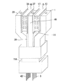
図1、2に示すように半導体パワーモジュールは、発熱体である能動素子7と受動素子6とがヒートパイプ1上に絶縁に必要な高さと面積を持つように形成された平面突起4に合わせて配置され、その上に、絶縁板11が能動素子7、受動素子6が配置される領域を避けて、すなわち能動素子7、受動素子6の周辺に備えられる。ここで半導体素子としての能動素子7、受動素子6は、表面に第1電極、裏面に第2電極(ともに図示せず)が形成されており、当該第1電極、第2電極を介して、ヒートパイプ1、後述のヒートパイプ20と電気的に接続されるものである。絶縁板11は、硬質の樹脂モールド等の絶縁体である。平面突起4および後述する平面突起22の高さは、並列する能動素子7、受動素子6の厚みの差を吸収することもでき、絶縁板11は能動素子7、受動素子6の配置位置を規制する。ここで、能動素子7、受動素子6がヒートパイプ1上に配置された位置を含む領域を第1領域とする。
As shown in FIGS. 1 and 2, the semiconductor power module is aligned with the planar protrusion 4 formed on the
ヒートパイプ1と絶縁板11とには、例えば位置決め突起3とそれに対応する位置決め穴12とを備えることができ、互いの位置関係を固定することができる。絶縁板11の能動素子7側の外側には中継端子ホルダ部9が備えられ、中継端子ホルダ部9を介して中継端子8が能動素子7の制御信号パット(図示せず)へ誘導され、直接接続される。中継端子ホルダ部9は絶縁板11を介してヒートパイプ1またはヒートパイプ20に固定されているが、中継端子ホルダ部9と絶縁板11とは別体としてもよく、これにより素子の位置決めと中継端子8の接続とを別工程で実施できるため、組立性を向上することができる。
The
中継端子8は、能動素子7の制御信号パットとの接触部分を丸く突起させることにより、能動素子7との接点の劣化を防ぐ。また中継端子8には弾性のある導電性の金属を用い、中継端子8の能動素子7との接点高さを能動素子7上面より若干低くなる高さとすることにより、中継端子8の弾性にて安定的に接点の接触が得られる。
The
また、中継端子8と能動素子7を、ワイヤーボンドや半田付けにて接続することもできる。能動素子7の半田付けの際にヒートパイプ1、ヒートパイプ20が過加熱される場合は、アセンブリ完了後にヒートパイプ1、ヒートパイプ20内に後述の冷媒を封入する方法で、ヒートパイプ1、ヒートパイプ20への過加熱を回避できる。
Further, the
図に示す場合では、ヒートパイプ1の側面には固定突起5が備えられ、固定突起5に備えられた位置決め突起10を用いて位置決めされ、同様に備えられた穴にネジ23が通され、ヒートパイプ1と絶縁板11とが固定される。
In the case shown in the figure, a fixing projection 5 is provided on the side surface of the
ヒートパイプ1は受動素子6側の延長上で下方に屈曲しており、屈曲した領域上に絶縁板13が備えられる。ヒートパイプ1の屈曲した領域と絶縁板13とには、例えば位置決め穴2とそれに対応する位置決め突起14とを備えることが可能であり、互いの位置関係を固定することができる。絶縁板13上、すなわちヒートパイプ1上の第1領域に対する他端側に対応する第2領域には冷却フィン15が備えられ、この冷却フィン15と絶縁板13とにも、例えば位置決め穴16とそれに対応する位置決め突起14とを備えることが可能であり、互いの位置関係を固定することができる。
The
図においては、冷却フィン15上にも同様に絶縁板17が位置決め穴16、位置決め突起18を介して備えられ、さらにその上に、ヒートパイプ20が、ヒートパイプ1と鏡対称となるように屈曲して位置決め穴19、位置決め突起18を介して絶縁板17との位置関係を固定されて備えられている。冷却フィン15をヒートパイプ1、ヒートパイプ20で挟み込むような構造となる。
In the figure, the
ヒートパイプ20は、能動素子7、受動素子6上に絶縁に必要な高さと面積を持つように形成した平面突起22を配置して位置決め突起21、位置決め穴12を介して覆いかぶさるように備えられる。
The
さらに能動素子7、受動素子6が配置される領域をガタなく覆うようにケース24が備えられる。ケース24は樹脂等からなる硬質絶縁体であり、ケース24に備えられた位置決め穴32と、ヒートパイプ1に対応して備えられた位置決め突起31とを合わせ、その弾性により締結を安定化させる押さえバネ30、平面突起29、樹脂等からなる硬質絶縁体のフタ27を順に乗せてネジ28で固定することができる。また、側面からは、貫通穴33に中継端子8を通して樹脂等からなる硬質絶縁体のフタ25を合わせ、ネジ26で固定する。能動素子7、受動素子6、ヒートパイプ1、ヒートパイプ20、ケース24の組立体は、導電性接合材なしに実現することが可能である。図2に示すように、ケース24で覆った領域を受熱部52、冷却フィン15を覆った領域を放熱部53とする。
Further, a
ヒートパイプ1、ヒートパイプ20は導電性の材質であり、平面な表面を有する。内部は空洞であり、冷媒が封入されている。尚、低出力、低発熱の半導体パワーモジュールである場合、ヒートパイプ1、ヒートパイプ20の片方または両方を、上記の空洞、冷媒等を備えていない通常の導体に置き換えても良い。冷媒は、受熱部52で気化し、放熱部53で液化することで熱交換を行う。ヒートパイプ1、ヒートパイプ20は、気化熱冷却構造となっている。
The
またヒートパイプ1、ヒートパイプ20は、絶縁板11と冷却フィン15の隙間(図2のA)での絶縁沿面距離を確保し、かつ冷却フィン15および絶縁板13、絶縁板17の厚みを吸収するため、放熱部53付近にてヒートパイプ1、ヒートパイプ20間の距離が大きくなる方向(互いに離れる方向)に屈曲した段差形状を持つ。すなわち、能動素子7、受動素子6が配置された位置を含む領域である第1領域よりも、第1領域に対応する他端の第2領域が厚みが厚くなる。このように形成することで、モジュールの大きさが増大することを抑制しつつ絶縁性を確保できる。なお、ヒートパイプ1、ヒートパイプ20のいずれか一方が屈曲した形状であってもよい。
Further, the
絶縁板11の厚さは、能動素子7、受動素子6の接合部分の絶縁沿面距離を確保し、且つ、ヒートパイプ1、ヒートパイプ20で絶縁板11を挟んだとき、能動素子7、受動素子6の接合部分の隙間の高さと一致する厚さとする。またヒートパイプ1、ヒートパイプ20は、端部に外部配線接続のためのネジ穴34、ネジ穴35を有する。
The thickness of the insulating
受動素子6、能動素子7は、あらかじめヒートパイプ1の平面突起4上に配置し、その上から絶縁板11をかぶせる。これにより、受動素子6、能動素子7を半田付けしない場合でも、位置決め突起3、位置決め穴12により、水平方向の位置ずれを抑制できる。
The
絶縁板13、絶縁板17は、例えば高熱伝導率のセラミック等でできた薄板であり、成型または接着により上下両面に位置決め突起14、位置決め突起18を有し、熱伝導グリース(図示なし)を介してヒートパイプ1、ヒートパイプ20と冷却フィン15とに密着する。
The insulating
冷却フィン15は例えば高熱伝導率の金属からなり、内部の冷媒流路にフィン状の突起を有することにより放熱効果を高めることができる。冷却フィン15は、両開口部に嵌合構造を持ち、隣り合う同じフィン構造と接続可能とする。また、嵌合構造は、パッキンやOリング等にて液体冷媒がもれない構造となっている。
The cooling
ヒートパイプ1、ヒートパイプ18間に挟まれる絶縁板11、絶縁板13、絶縁板17及び冷却フィン15は全て、位置決め突起3、位置決め突起14、位置決め突起18、位置決め突起21及び位置決め穴2、位置決め穴12、位置決め穴16、位置決め穴19により互いに位置決めされることにより、位置ずれ発生を防止できる。
The insulating
構造全体で半田等の導電性の接合材を使用しないで組み立てることができることにより、製造コストを下げ、半田クラック等による信頼性低下を防止する効果がある。 Since the entire structure can be assembled without using a conductive bonding material such as solder, the manufacturing cost can be reduced and the reliability can be prevented from being lowered due to solder cracks or the like.
ただ、受動素子6と能動素子7をヒートパイプ1、ヒートパイプ20に半田付けし、中継端子8と能動素子7の接点を半田付けした場合には、ケース24、フタ25、フタ27の代わりに樹脂モールドにて一体化することもできる。
However, when the
図3は、本発明にかかる半導体パワーモジュール(1in1回路モジュール)の完成図である。放熱部53を覆うケース24等には、ケース同士を締結する後述のモジュール締結金具109、モジュール締結金具115(図6参照)を挿入する締結溝154を設ける。締結溝154は、放熱部53を覆うケース24、フタ27の表面に設けることによりモジュール同士を任意の順に締結できる。
FIG. 3 is a completed view of the semiconductor power module (1 in 1 circuit module) according to the present invention. The
<A−2.効果>
本発明にかかる実施の形態1によれば、半導体パワーモジュールにおいて、表面に第1電極、裏面に第2電極が形成された半導体素子としての能動素子7、受動素子6と、一端側に能動素子7、受動素子6が配置される第1領域が規定され、当該第1領域に配置された能動素子7、受動素子6の第1、第2電極の一方と電気的に接続される第1ヒートパイプとしてのヒートパイプ1と、ヒートパイプ1の他端側に規定される第2領域に配置された冷却フィン15と、ヒートパイプ1上に配置された能動素子7、受動素子6および冷却フィン15をヒートパイプ1とで挟み込み、能動素子7、受動素子6の第1、第2電極の他方と電気的に接続された第2ヒートパイプとしてのヒートパイプ20とを備えることで、モジュール自体を大きくすることなく、十分な放熱性能を実現することが可能となる。
<A-2. Effect>
According to the first embodiment of the present invention, in a semiconductor power module, an
また、本発明にかかる実施の形態1によれば、半導体パワーモジュールにおいて、第1領域において半導体素子としての能動素子7、受動素子6周辺に配置され、当該能動素子7、受動素子6の配置位置を規制する第1絶縁板としての絶縁板11をさらに備え、絶縁板11は、第1または第2ヒートパイプとしてのヒートパイプ1、ヒートパイプ20に対し位置決めされることで、位置ずれの発生が抑制され、信頼性が向上する。なお、このように位置決めされた絶縁板11が備えられない場合であっても、モジュール自体を大きくすることなく、十分な放熱性能を実現することは可能である。
Further, according to the first embodiment of the present invention, in the semiconductor power module, the
また、本発明にかかる実施の形態1によれば、半導体パワーモジュールにおいて、第1絶縁板としての絶縁板11および第1、第2ヒートパイプとしてのヒートパイプ1、ヒートパイプ20は、それぞれ対応する第1嵌合部としての位置決め突起3、位置決め穴12、位置決め突起21をさらに備えることで、位置ずれの発生が抑制され、信頼性が向上する。なお、このような第1嵌合部が備えられない場合であっても、ヒートパイプ1、ヒートパイプ20および絶縁板11の位置関係が固定されればよく、またそのような固定がされない場合でも、モジュール自体を大きくすることなく、十分な放熱性能を実現することは可能である。
Further, according to the first embodiment of the present invention, in the semiconductor power module, the insulating
また、本発明にかかる実施の形態1によれば、半導体パワーモジュールにおいて、第2領域において、冷却フィン15と第1および第2ヒートパイプとしてのヒートパイプ1、ヒートパイプ20との間にそれぞれ配置され、冷却フィン15の配置位置を規制する第2、第3絶縁板としての絶縁板13、絶縁板17をさらに備え、絶縁板13、絶縁板17は、それぞれヒートパイプ1、ヒートパイプ20に対し位置決めされることで、位置ずれの発生が抑制され、信頼性が向上する。なお、このように位置決めされた絶縁板13、絶縁板17が備えられない場合であっても、モジュール自体を大きくすることなく、十分な放熱性能を実現することは可能である。
Further, according to the first embodiment of the present invention, in the semiconductor power module, the second region is arranged between the cooling
また、本発明にかかる実施の形態1によれば、半導体パワーモジュールにおいて、第2、第3絶縁板としての絶縁板13、絶縁板17および第1および第2ヒートパイプとしてのヒートパイプ1、ヒートパイプ20は、それぞれ対応する第2嵌合部としての位置決め穴2、位置決め突起14、位置決め穴16、位置決め突起18、位置決め穴19をさらに備えることで、位置ずれの発生が抑制され、信頼性が向上する。なお、このような第2嵌合部が備えられない場合であっても、ヒートパイプ1、ヒートパイプ20および絶縁板13、絶縁板17の位置関係が固定されればよく、またそのような固定がされない場合でも、モジュール自体を大きくすることなく、十分な放熱性能を実現することは可能である。
Further, according to the first embodiment of the present invention, in the semiconductor power module, the insulating
また、本発明にかかる実施の形態1によれば、半導体パワーモジュールにおいて、半導体素子としての能動素子7、受動素子6に接続される中継端子8を誘導する中継端子ホルダ部9をさらに備え、中継端子ホルダ部9は、第1領域の外端側において第1または第2ヒートパイプとしてのヒートパイプ1、ヒートパイプ20に固定されることで、中継端子8が中継端子ホルダ部9を介して能動素子7に安定して接続され、モジュールの信頼性が向上する。なお、このような中継端子8を誘導する中継端子ホルダ部9が備えられない場合であっても、モジュール自体を大きくすることなく、十分な放熱性能を実現することは可能である。
Further, according to the first embodiment of the present invention, the semiconductor power module further includes the relay
また、本発明にかかる実施の形態1によれば、半導体パワーモジュールにおいて、第1領域において半導体素子としての能動素子7、受動素子6周辺に配置され、当該能動素子7、受動素子6の配置位置を規制する第1絶縁板としての絶縁板11が備えられる場合に、中継端子ホルダ部9は絶縁板11と一体として形成されることで、中継端子8が中継端子ホルダ部9を介して能動素子7に安定して接続され、モジュールの信頼性が向上する。なお、このように中継端子ホルダ部9が絶縁板11と一体として備えられない場合であっても、モジュール自体を大きくすることなく、十分な放熱性能を実現することは可能である。
Further, according to the first embodiment of the present invention, in the semiconductor power module, the
また、本発明にかかる実施の形態1によれば、半導体パワーモジュールにおいて、第1、第2ヒートパイプとしてのヒートパイプ1、ヒートパイプ20は、内部の空洞に冷媒を備えることで、中継端子8と能動素子7を、ワイヤーボンドや半田付けにて接続する場合に、ヒートパイプ1、ヒートパイプ20を加熱するとき、アセンブリ完了後にヒートパイプ1、ヒートパイプ20内に冷媒を封入する方法で、ヒートパイプ1、ヒートパイプ20への過加熱を回避することができる。なお、このようにヒートパイプ1、ヒートパイプ20に冷媒を入れる空洞が備えられない場合であっても、モジュール自体を大きくすることなく、十分な放熱性能を実現することは可能である。
Further, according to the first embodiment of the present invention, in the semiconductor power module, the
また、本発明にかかる実施の形態1によれば、半導体パワーモジュールにおいて、第1領域に配設され、半導体素子としての能動素子7、受動素子6および第1、第2ヒートパイプとしてのヒートパイプ1、ヒートパイプ20を覆うケース24をさらに備え、能動素子7、受動素子6、ヒートパイプ1、ヒートパイプ20およびケース24の組立体は導電性接合材なしに実現されることで、半田クラック等による信頼性の低下を抑制することができる。なお、このようなケース24を備えない場合でも、モジュール自体を大きくすることなく、十分な放熱性能を実現することは可能である。
In addition, according to the first embodiment of the present invention, in the semiconductor power module, the
また、本発明にかかる実施の形態1によれば、半導体パワーモジュールにおいて、第2領域の厚みは、第1領域の厚みよりも大きく、第1、第2ヒートパイプとしてのヒートパイプ1、ヒートパイプ20の少なくとも一方は、第1領域から第2領域にかけて斜めに傾斜した面を有する段差形状であることで、モジュールの大きさが増大することを抑制しつつ絶縁性を確保できる。
Further, according to the first embodiment of the present invention, in the semiconductor power module, the thickness of the second region is larger than the thickness of the first region, and the
<B.実施の形態2>
<B−1.構成>
図4は、本発明にかかる半導体パワーモジュール(2in1回路モジュール)の組立後の断面図である。実施の形態1と同様である構成については詳細な説明を省略する。
<B. Second Embodiment>
<B-1. Configuration>
FIG. 4 is a cross-sectional view of the semiconductor power module (2-in-1 circuit module) according to the present invention after assembly. Detailed description of the same configuration as that of the first embodiment will be omitted.
ヒートパイプ46は、導電性の材質であり、平面な表面を有する。内部は空洞であり、冷媒が封入されている。尚、低出力で低発熱の半導体パワーモジュールの場合、ヒートパイプ1、ヒートパイプ20は、片方または、両方を上記の空洞、冷媒等を備えていない通常の導体に置き換えても良い。冷媒は、受熱部54で気化し、放熱部55で液化することで熱交換を行う。ヒートパイプ46は、気化熱冷却構造となっている。
The
ヒートパイプ46は、能動素子7および受動素子6、別の半導体素子としての能動素子42および受動素子41上に絶縁に必要な高さと面積を持つように形成した平面突起を配置して位置決め突起、位置決め穴を介して覆いかぶさるように備えられる。平面突起の高さは、並列する能動素子7、能動素子42、受動素子6、受動素子41の厚みの差を吸収することもできる。
The
第3ヒートパイプとしてのヒートパイプ46は屈曲しないが、ヒートパイプ1、ヒートパイプ20は、絶縁板11、絶縁板39と冷却フィン15、冷却フィン48の隙間(図4のB)での絶縁沿面距離を確保し、かつ冷却フィン15、冷却フィン48と絶縁板13、絶縁板17、絶縁板37、絶縁板38の厚みを吸収するため、冷却フィン付近にてヒートパイプ46との距離が大きくなる方向(互いに離れる方向)に屈曲した段差形状を持つ。このように形成することで、モジュールの大きさを維持しつつ絶縁性を確保できる。なお、ヒートパイプ1、ヒートパイプ20のいずれか一方が屈曲した形状であってもよい。
The
またヒートパイプ1、ヒートパイプ20、ヒートパイプ46は、外部配線接続のため、それぞれネジ穴34、ネジ穴47、ネジ穴35を有する。
The
能動素子7と受動素子6及び絶縁板11と絶縁板13、絶縁板17にはさまれる冷却フィン15は、それぞれ位置決め穴と位置決め突起にて位置決めされた状態で、ヒートパイプ1とヒートパイプ46にはさまれる。
The cooling
また能動素子42と受動素子41及び、絶縁板39と絶縁板37、絶縁板38にはさまれる冷却フィン48は、それぞれ位置決め穴と位置決め突起にて位置決めされ、ヒートパイプ46とヒートパイプ20にはさまれる。これにより2in1回路構造を持ったモジュールとなる。
Further, the
硬質の樹脂モールド等の絶縁体である絶縁板39は、絶縁板11と同じく、その能動素子42側には中継端子ホルダ部44が備えられ、中継端子ホルダ部44を介して中継端子43が能動素子42の制御信号パット(図示せず)と直接接続される。中継端子ホルダ44と絶縁板39を別体としてもよく、これにより、素子位置決めと中継端子接続を別工程で実施できるため、組立性を向上することができる。
As with the insulating
中継端子43は、能動素子42の制御信号パットとの接触部分を丸く突起させることにより、能動素子42との接点の劣化を防ぐ。また、中継端子43には弾性のある導電性の金属を用い、中継端子43の能動素子42との接点高さを能動素子42上面より若干低くなる高さとすることにより、中継端子43の弾性にて安定な接点の接触が得られる。また、中継端子43と能動素子42を、ワイヤーボンドや半田付けにて接続することもできる。
The
ケース45は、例えば樹脂等からなる硬質絶縁体であり、ヒートパイプ20との位置決め突起31と嵌合する位置決め穴にてヒートパイプ1と位置決めされる。また、ケース45の開口幅を、ケース45へ挿入する受熱部54(図4)とのガタが無いようにすることにより、ケース45への挿入後の受熱部54の位置ずれをなくすことができる。
The
フタ51は、樹脂等からなる硬質絶縁体であり、貫通穴49、貫通穴50に、中継端子8、中継端子43を貫通させ、ケース45にネジ止めされる。
The
フタ27は、樹脂等からなる硬質絶縁体であり、ケース45に組み付けられたユニットのヒートパイプ20側からケース45に取り付けられる。ヒートパイプ20とフタ27間に、押さえバネ(図示なし)等の弾性物を挿入することで、さらに締結を安定化することもできる。
The
構造全体で半田等の導電性の接合材を使用しないで組み立てることができることにより、製造コストを下げ、半田クラック等による信頼性低下を防止する効果がある。 Since the entire structure can be assembled without using a conductive bonding material such as solder, the manufacturing cost can be reduced and the reliability can be prevented from being lowered due to solder cracks or the like.
ただ、受動素子6、受動素子41と能動素子7、能動素子42をヒートパイプ1、ヒートパイプ20、ヒートパイプ46に半田付けし、中継端子8と能動素子7及び、中継端子43と能動素子42の接点をワイヤーボンドや半田付けにて接続した場合、ケース45、フタ27、フタ51の代わりに樹脂モールドにて一体化することもできる。
However, the
図5は、本発明にかかる半導体パワーモジュール(2in1回路モジュール)の完成図である。放熱部55を覆うケース45等には、ケース同士を締結する後述のモジュール締結金具109、モジュール締結金具115(図6参照)を挿入する締結溝154を設けられる。締結溝154は、放熱部55を覆うケース45、フタ27の表面に設けられることによりモジュール同士を任意の順に締結できる。
FIG. 5 is a completed view of the semiconductor power module (2-in-1 circuit module) according to the present invention. The
<B−2.効果>
本発明にかかる実施の形態2によれば、半導体パワーモジュールにおいて、第2ヒートパイプとしてのヒートパイプ20上に配置された別の半導体素子としての能動素子42、受動素子41および別の冷却フィン48と、別の能動素子42、受動素子41および別の冷却フィン48をヒートパイプ20とで挟み込む第3ヒートパイプとしてのヒートパイプ46とをさらに備えることで、2つの単位モジュールを1つに締結した2in1回路モジュールを形成することができる。なお、このように能動素子42、受動素子41をさらに備えないような場合には、実施の形態1に示したような構造と同様であり、モジュール自体を大きくすることなく、十分な放熱性能を実現することが可能である。
<B-2. Effect>
According to the second embodiment of the present invention, in a semiconductor power module, an
<C.実施の形態3>
<C−1.構成>
図6は、本発明にかかる半導体パワーモジュール(6in1インバータ−)の組立図である。6in1インバータ−とは、実施の形態1に示した1in1回路モジュールを6個結合した回路構成である。
<
<C-1. Configuration>
FIG. 6 is an assembly diagram of a semiconductor power module (6 in 1 inverter) according to the present invention. The 6-in-1 inverter is a circuit configuration in which six 1-in-1 circuit modules shown in the first embodiment are combined.
各1in1モジュール(単位モジュール101)の放熱部のケースには、ケース同士を締結する締結具としてのモジュール締結金具109、モジュール締結金具115を挿入する締結溝154を設ける。締結溝154は、締結方向を4方向とするため、放熱部の側面に設ける。
The case of the heat radiation part of each 1 in 1 module (unit module 101) is provided with a
図に示すように、W、V、U各相のP側、N側の電極を連結するW相電極連結ブスバー103、V相電極連結ブスバー104、U相電極連結ブスバー105が配置される。インバータのP電源側の電極はP側連結ブスバー102で接続され、N電源側の電極はN側連結ブスバー106で各モジュールに接続される。
As shown in the figure, a W-phase electrode
モジュール締結金具109、モジュール締結金具115は単位モジュール101間に挿入される相間絶縁板117にそれぞれネジ116で止めることにより、単位モジュール101の締結を行う。
The
冷却フィン部分は、P側、N側にそれぞれ非導体の冷却部締結板108、冷却部締結板118を配置し、冷却部を貫通する、非導体または絶縁処理された冷却部締結ネジ107で締め付けることにより締結される。
The cooling fin portion is provided with a non-conductor cooling
シールド板112と制御基板113は、モールド部下面に取り付けるスペーサ110およびネジ114によって固定される。
The
図7は、実施の形態1に示した1in1モジュールを単位モジュール101として6個を結合した、6in1インバータモジュール完成図である。一方図8は、実施の形態2に示した2in1モジュールを単位モジュール119として6個を結合した、6in1インバータモジュール完成図である。
FIG. 7 is a completed diagram of a 6 in 1 inverter module in which six 1 in 1 modules shown in the first embodiment are combined as a
以上の方法により、半導体パワー部の冷却と配線構造を一体とし、さらに素子自体を両面冷却でき、連結可能な小型モジュールを組み合わせることにより小型且つ、高出力なインバータモジュールを提供できる。 By the above method, the cooling of the semiconductor power unit and the wiring structure are integrated, the element itself can be cooled on both sides, and a small and high output inverter module can be provided by combining small modules that can be connected.
<C−2.効果>
本発明にかかる実施の形態3によれば、半導体パワーモジュールにおいて、上記の複数個の半導体パワーモジュールと、複数個の半導体パワーモジュールを一体に締結する締結具としてのモジュール締結金具109、モジュール締結金具115、ネジ116とを備えることで、例えば6つの単位モジュールを1つに締結した6in1回路モジュール(図6等参照)を形成することができる。なお、このように複数個の半導体モジュールを一体に締結せずとも、実施の形態1に示すようにモジュール自体を大きくすることなく、十分な放熱性能を実現することは可能である。
<C-2. Effect>
According to the third embodiment of the present invention, in the semiconductor power module, the plurality of semiconductor power modules, the
本発明の実施の形態では、各構成要素の材質、材料、実施の条件等についても記載しているが、これらは例示であって記載したものに限られるものではない。 In the embodiment of the present invention, the material, material, conditions for implementation, etc. of each component are also described, but these are examples and are not limited to those described.
1,20,46 ヒートパイプ、2,12,16,19,32 位置決め穴、3,10,14,18,21,31 位置決め突起、4,22,29 平面突起、5 固定突起、6,41,202 受動素子、7,42,201 能動素子、8,43,210 中継端子、9,44 中継端子ホルダ部、11,13,17,37〜39,205 絶縁板、15,48,209 冷却フィン、23,26,28,114,116 ネジ、24,45 ケース、25,27,51 フタ、30 押さえバネ、33,49,50 貫通穴、34,35,47 ネジ穴、52,54 受熱部、53,55 放熱部、101,119 単位モジュール、107 冷却部締結ネジ、108,118 冷却部締結板、109,115 モジュール締結金具、110 スペーサ、112 シールド板、113 制御基板、117 相間絶縁板、154 締結溝、203 アルミワイヤー、204 アルミパターン、206 コレクタ電極板、207 エミッタ電極板、208 外部ブスバー、211 ヒートスプレッダ。
1, 20, 46 Heat pipe, 2, 12, 16, 19, 32 Positioning hole, 3, 10, 14, 18, 21, 31 Positioning protrusion, 4, 22, 29 Planar protrusion, 5 Fixing protrusion, 6, 41, 202 Passive element, 7, 42, 201 Active element, 8, 43, 210 Relay terminal, 9, 44 Relay terminal holder part, 11, 13, 17, 37-39, 205 Insulating plate, 15, 48, 209 Cooling fin, 23, 26, 28, 114, 116 Screw, 24, 45 Case, 25, 27, 51 Lid, 30 Pressing spring, 33, 49, 50 Through hole, 34, 35, 47 Screw hole, 52, 54 Heat receiving part, 53 , 55 Heat radiation part, 101, 119 Unit module, 107 Cooling part fastening screw, 108, 118 Cooling part fastening plate, 109, 115 Module fastening bracket, 110 Spacer, 12 shield plate, 113 control substrate, 117 interphase insulating plate, 154 coupling groove, 203 aluminum wire, 204 aluminum pattern, 206 a collector electrode plate, 207 an emitter electrode plate, 208
Claims (12)
一端側に前記半導体素子が配置される第1領域が規定され、当該第1領域に配置された前記半導体素子の前記第1、第2電極の一方と電気的に接続される第1ヒートパイプと、
前記第1ヒートパイプの他端側に規定される第2領域に配置された冷却フィンと、
前記第1ヒートパイプ上に配置された前記半導体素子および前記冷却フィンを前記第1ヒートパイプとで挟み込み、前記半導体素子の前記第1、第2電極の他方と電気的に接続された第2ヒートパイプとを備える、
半導体パワーモジュール。 A semiconductor element having a first electrode on the front surface and a second electrode on the back surface;
A first region in which the semiconductor element is disposed on one end side, and a first heat pipe electrically connected to one of the first and second electrodes of the semiconductor element disposed in the first region; ,
Cooling fins disposed in a second region defined on the other end of the first heat pipe;
A second heat that is sandwiched between the first heat pipe and the semiconductor element disposed on the first heat pipe and electrically connected to the other of the first and second electrodes of the semiconductor element. With pipes,
Semiconductor power module.
前記第1絶縁板は、前記第1または第2ヒートパイプに対し位置決めされる、
請求項1に記載の半導体パワーモジュール。 A first insulating plate disposed around the semiconductor element in the first region and restricting a position of the semiconductor element;
The first insulating plate is positioned with respect to the first or second heat pipe;
The semiconductor power module according to claim 1.
請求項2に記載の半導体パワーモジュール。 The first insulating plate and the first and second heat pipes further include corresponding first fitting portions, respectively.
The semiconductor power module according to claim 2.
前記第2、第3絶縁板は、それぞれ前記第1および第2ヒートパイプに対し位置決めされる、
請求項1〜3のいずれかに記載の半導体パワーモジュール。 The second region further includes second and third insulating plates that are arranged between the cooling fins and the first and second heat pipes, respectively, and restrict the arrangement positions of the cooling fins,
The second and third insulating plates are positioned with respect to the first and second heat pipes, respectively.
The semiconductor power module in any one of Claims 1-3.
請求項4に記載の半導体パワーモジュール。 The second and third insulating plates and the first and second heat pipes further include corresponding second fitting portions, respectively.
The semiconductor power module according to claim 4.
前記中継端子ホルダ部は、前記第1領域の外端側において前記第1または第2ヒートパイプに固定される、
請求項1〜5のいずれかに記載の半導体パワーモジュール。 A relay terminal holder for guiding a relay terminal connected to the semiconductor element;
The relay terminal holder portion is fixed to the first or second heat pipe on the outer end side of the first region.
The semiconductor power module according to claim 1.
請求項6に記載の半導体パワーモジュール。 The relay terminal holder portion is formed integrally with the first insulating plate when the first insulating plate is disposed around the semiconductor element in the first region and regulates the position of the semiconductor element.
The semiconductor power module according to claim 6.
請求項1〜7のいずれかに記載の半導体パワーモジュール。 The first and second heat pipes include a refrigerant in an internal cavity,
The semiconductor power module according to claim 1.
前記半導体素子、前記第1、第2ヒートパイプおよび前記ケースの組立体は導電性接合材なしに実現される、
請求項1〜8のいずれかに記載の半導体パワーモジュール。 A case disposed in the first region and further covering the semiconductor element and the first and second heat pipes;
The assembly of the semiconductor element, the first and second heat pipes and the case is realized without a conductive bonding material.
The semiconductor power module according to claim 1.
前記別の半導体素子および前記別の冷却フィンを前記第2ヒートパイプとで挟み込む第3ヒートパイプとをさらに備える、
請求項1〜9のいずれかに記載の半導体パワーモジュール。 Another semiconductor element and another cooling fin disposed on the second heat pipe;
A third heat pipe sandwiching the another semiconductor element and the another cooling fin with the second heat pipe;
The semiconductor power module according to claim 1.
前記複数個の半導体パワーモジュールを一体に締結する締結具とを備える、
半導体パワーモジュール。 A plurality of semiconductor power modules according to any one of claims 1 to 10,
A fastener for integrally fastening the plurality of semiconductor power modules;
Semiconductor power module.
前記第1、第2ヒートパイプの少なくとも一方は、前記第1領域から前記第2領域にかけて斜めに傾斜した面を有する段差形状である、
請求項1〜11のいずれかに記載の半導体パワーモジュール。 The thickness of the second region is larger than the thickness of the first region,
At least one of the first and second heat pipes has a step shape having a surface inclined obliquely from the first region to the second region.
The semiconductor power module according to claim 1.
Priority Applications (3)
| Application Number | Priority Date | Filing Date | Title |
|---|---|---|---|
| JP2010182727A JP5489911B2 (en) | 2010-08-18 | 2010-08-18 | Semiconductor power module |
| US13/114,475 US8648462B2 (en) | 2010-08-18 | 2011-05-24 | Semiconductor power module |
| CN201110237469.3A CN102376661B (en) | 2010-08-18 | 2011-08-18 | Semiconductor power module |
Applications Claiming Priority (1)
| Application Number | Priority Date | Filing Date | Title |
|---|---|---|---|
| JP2010182727A JP5489911B2 (en) | 2010-08-18 | 2010-08-18 | Semiconductor power module |
Publications (3)
| Publication Number | Publication Date |
|---|---|
| JP2012043915A true JP2012043915A (en) | 2012-03-01 |
| JP2012043915A5 JP2012043915A5 (en) | 2013-05-02 |
| JP5489911B2 JP5489911B2 (en) | 2014-05-14 |
Family
ID=45593408
Family Applications (1)
| Application Number | Title | Priority Date | Filing Date |
|---|---|---|---|
| JP2010182727A Expired - Fee Related JP5489911B2 (en) | 2010-08-18 | 2010-08-18 | Semiconductor power module |
Country Status (3)
| Country | Link |
|---|---|
| US (1) | US8648462B2 (en) |
| JP (1) | JP5489911B2 (en) |
| CN (1) | CN102376661B (en) |
Cited By (3)
| Publication number | Priority date | Publication date | Assignee | Title |
|---|---|---|---|---|
| WO2015111211A1 (en) * | 2014-01-27 | 2015-07-30 | 株式会社日立製作所 | Power module and manufacturing method therefor |
| WO2016060123A1 (en) * | 2014-10-14 | 2016-04-21 | 矢崎総業株式会社 | Service plug |
| JP2016143472A (en) * | 2015-01-30 | 2016-08-08 | 矢崎総業株式会社 | Service plug |
Families Citing this family (11)
| Publication number | Priority date | Publication date | Assignee | Title |
|---|---|---|---|---|
| AU2012232967B2 (en) * | 2011-10-31 | 2015-01-15 | Abb Technology Ag | Cabinet with modules having a thermosiphon cooler arrangement |
| AU2012232968B2 (en) | 2011-10-31 | 2014-11-13 | Abb Technology Ag | Thermosiphon cooler arrangement in modules with electric and/or electronic components |
| DE102011088053B3 (en) * | 2011-12-08 | 2013-04-11 | Siemens Aktiengesellschaft | transmitters |
| JP2016134408A (en) * | 2015-01-16 | 2016-07-25 | 矢崎総業株式会社 | Semiconductor breaker |
| CN107852833B (en) * | 2015-09-29 | 2020-10-20 | 日立汽车系统株式会社 | Electronic control device and method for manufacturing in-vehicle electronic control device |
| CN108257931B (en) * | 2018-01-18 | 2019-11-01 | 上海理工大学 | A kind of integrated circuit plate heat dissipating device and its integrated circuit board |
| CN110244014B (en) * | 2019-07-15 | 2024-08-16 | 石家庄铁路职业技术学院 | Water quality detector based on open source hardware |
| US11967899B2 (en) | 2020-05-22 | 2024-04-23 | Marel Power Solutions | Fluid cooled inverter |
| EP3955285A1 (en) * | 2020-08-14 | 2022-02-16 | Siemens Aktiengesellschaft | Power module and device for cooling a power module |
| US20240251533A1 (en) * | 2021-09-15 | 2024-07-25 | Marel Power Solutions, Inc. | Air cooled compact power systems |
| EP4402789A1 (en) * | 2021-09-15 | 2024-07-24 | Marel Power Solutions, Inc. | Compact power converter |
Citations (6)
| Publication number | Priority date | Publication date | Assignee | Title |
|---|---|---|---|---|
| JPH03231446A (en) * | 1990-02-07 | 1991-10-15 | Ngk Insulators Ltd | Semiconductor element for power use |
| JPH0653679A (en) * | 1991-09-13 | 1994-02-25 | Furukawa Electric Co Ltd:The | Heat pipe type radiator and cooling structure of heat generator |
| JPH088398A (en) * | 1994-06-20 | 1996-01-12 | Toshiba Transport Eng Kk | Power semiconductor element unit |
| JP2006134990A (en) * | 2004-11-04 | 2006-05-25 | Fuji Electric Holdings Co Ltd | Semiconductor apparatus |
| JP2007310716A (en) * | 2006-05-19 | 2007-11-29 | Toshiba Corp | Electronic apparatus |
| JP2009088386A (en) * | 2007-10-02 | 2009-04-23 | Rohm Co Ltd | Power module |
Family Cites Families (20)
| Publication number | Priority date | Publication date | Assignee | Title |
|---|---|---|---|---|
| US2754455A (en) * | 1952-11-29 | 1956-07-10 | Rca Corp | Power Transistors |
| SE354943B (en) * | 1970-02-24 | 1973-03-26 | Asea Ab | |
| GB1346157A (en) * | 1971-02-13 | 1974-02-06 | Bbc Brown Boveri & Cie | Cooling apparatus for a thyristor |
| US3978518A (en) * | 1975-11-12 | 1976-08-31 | Rca Corporation | Reinforced transcalent device |
| US4386362A (en) * | 1979-12-26 | 1983-05-31 | Rca Corporation | Center gate semiconductor device having pipe cooling means |
| JPH01155150A (en) * | 1987-12-11 | 1989-06-19 | Mitsubishi Electric Corp | Refrigerator |
| JPH03175479A (en) * | 1989-12-04 | 1991-07-30 | Mitsubishi Electric Corp | Image display device |
| JPH0473791A (en) * | 1990-07-16 | 1992-03-09 | Mitsubishi Electric Corp | Device and method for cooling display apparatus |
| US6005772A (en) * | 1997-05-20 | 1999-12-21 | Denso Corporation | Cooling apparatus for high-temperature medium by boiling and condensing refrigerant |
| JPH1140717A (en) | 1997-07-23 | 1999-02-12 | Furukawa Electric Co Ltd:The | Wiring material and cooling structure using the same |
| EP2234154B1 (en) * | 2000-04-19 | 2016-03-30 | Denso Corporation | Coolant cooled type semiconductor device |
| JP3669971B2 (en) | 2002-05-21 | 2005-07-13 | 三菱電機株式会社 | Semiconductor module |
| JP2005123265A (en) | 2003-10-14 | 2005-05-12 | Sumitomo Electric Ind Ltd | Power device cooling apparatus and inverter unit for motor driving |
| US7324341B2 (en) * | 2005-09-22 | 2008-01-29 | Delphi Technologies, Inc. | Electronics assembly and heat pipe device |
| US7417858B2 (en) * | 2005-12-21 | 2008-08-26 | Sun Microsystems, Inc. | Cooling technique using multiple magnet array for magneto-hydrodynamic cooling of multiple integrated circuits |
| US7532476B2 (en) * | 2006-06-29 | 2009-05-12 | Intel Corporation | Flow solutions for microelectronic cooling |
| JP4935220B2 (en) | 2006-07-21 | 2012-05-23 | 三菱マテリアル株式会社 | Power module device |
| JP2008124430A (en) * | 2006-10-18 | 2008-05-29 | Hitachi Ltd | Power semiconductor module |
| US7965508B2 (en) * | 2007-03-27 | 2011-06-21 | Denso Corporation | Cooling device for electronic component and power converter equipped with the same |
| JP5473733B2 (en) * | 2010-04-02 | 2014-04-16 | 株式会社日立製作所 | Power semiconductor module |
-
2010
- 2010-08-18 JP JP2010182727A patent/JP5489911B2/en not_active Expired - Fee Related
-
2011
- 2011-05-24 US US13/114,475 patent/US8648462B2/en not_active Expired - Fee Related
- 2011-08-18 CN CN201110237469.3A patent/CN102376661B/en not_active Expired - Fee Related
Patent Citations (6)
| Publication number | Priority date | Publication date | Assignee | Title |
|---|---|---|---|---|
| JPH03231446A (en) * | 1990-02-07 | 1991-10-15 | Ngk Insulators Ltd | Semiconductor element for power use |
| JPH0653679A (en) * | 1991-09-13 | 1994-02-25 | Furukawa Electric Co Ltd:The | Heat pipe type radiator and cooling structure of heat generator |
| JPH088398A (en) * | 1994-06-20 | 1996-01-12 | Toshiba Transport Eng Kk | Power semiconductor element unit |
| JP2006134990A (en) * | 2004-11-04 | 2006-05-25 | Fuji Electric Holdings Co Ltd | Semiconductor apparatus |
| JP2007310716A (en) * | 2006-05-19 | 2007-11-29 | Toshiba Corp | Electronic apparatus |
| JP2009088386A (en) * | 2007-10-02 | 2009-04-23 | Rohm Co Ltd | Power module |
Cited By (4)
| Publication number | Priority date | Publication date | Assignee | Title |
|---|---|---|---|---|
| WO2015111211A1 (en) * | 2014-01-27 | 2015-07-30 | 株式会社日立製作所 | Power module and manufacturing method therefor |
| US10080313B2 (en) | 2014-01-27 | 2018-09-18 | Hitachi, Ltd. | Power module and method for manufacturing the same |
| WO2016060123A1 (en) * | 2014-10-14 | 2016-04-21 | 矢崎総業株式会社 | Service plug |
| JP2016143472A (en) * | 2015-01-30 | 2016-08-08 | 矢崎総業株式会社 | Service plug |
Also Published As
| Publication number | Publication date |
|---|---|
| JP5489911B2 (en) | 2014-05-14 |
| CN102376661A (en) | 2012-03-14 |
| CN102376661B (en) | 2015-03-25 |
| US8648462B2 (en) | 2014-02-11 |
| US20120043652A1 (en) | 2012-02-23 |
Similar Documents
| Publication | Publication Date | Title |
|---|---|---|
| JP5489911B2 (en) | Semiconductor power module | |
| KR102048478B1 (en) | Power module of double-faced cooling and method for manufacturing thereof | |
| JP6237912B2 (en) | Power semiconductor module | |
| US8610263B2 (en) | Semiconductor device module | |
| JP6634778B2 (en) | Semiconductor device and manufacturing method thereof | |
| US8946882B2 (en) | Semiconductor module and semiconductor device | |
| CN102780386B (en) | Electronic equipment and the power conversion unit with electronic equipment | |
| JP2013123014A (en) | Semiconductor device | |
| JP5851599B2 (en) | Power module | |
| WO2020054376A1 (en) | Electric power converter | |
| JP4146888B2 (en) | Semiconductor module and method for manufacturing semiconductor module | |
| JP7379886B2 (en) | semiconductor equipment | |
| WO2020208867A1 (en) | Semiconductor device | |
| JP5267238B2 (en) | Semiconductor device and manufacturing method of semiconductor device | |
| JP2007073782A (en) | High power semiconductor apparatus | |
| WO2019189450A1 (en) | Power conversion device | |
| JP2021125545A (en) | Semiconductor module and method for manufacturing semiconductor module | |
| JP6590952B2 (en) | Semiconductor device | |
| JP2004247684A (en) | Heat sink and heat radiating device | |
| JP2015185835A (en) | Semiconductor device and manufacturing method of the same | |
| JP5717922B1 (en) | Power converter | |
| JP5125530B2 (en) | Power converter | |
| JP2011066281A (en) | Heat generating device | |
| JP2022162304A (en) | Semiconductor module and semiconductor apparatus | |
| JP2013143408A (en) | Semiconductor package and semiconductor device |
Legal Events
| Date | Code | Title | Description |
|---|---|---|---|
| A521 | Request for written amendment filed |
Free format text: JAPANESE INTERMEDIATE CODE: A523 Effective date: 20130315 |
|
| A621 | Written request for application examination |
Free format text: JAPANESE INTERMEDIATE CODE: A621 Effective date: 20130315 |
|
| A977 | Report on retrieval |
Free format text: JAPANESE INTERMEDIATE CODE: A971007 Effective date: 20131031 |
|
| A131 | Notification of reasons for refusal |
Free format text: JAPANESE INTERMEDIATE CODE: A131 Effective date: 20131112 |
|
| A521 | Request for written amendment filed |
Free format text: JAPANESE INTERMEDIATE CODE: A523 Effective date: 20140106 |
|
| TRDD | Decision of grant or rejection written | ||
| A01 | Written decision to grant a patent or to grant a registration (utility model) |
Free format text: JAPANESE INTERMEDIATE CODE: A01 Effective date: 20140128 |
|
| A61 | First payment of annual fees (during grant procedure) |
Free format text: JAPANESE INTERMEDIATE CODE: A61 Effective date: 20140225 |
|
| R150 | Certificate of patent or registration of utility model |
Ref document number: 5489911 Country of ref document: JP Free format text: JAPANESE INTERMEDIATE CODE: R150 |
|
| R250 | Receipt of annual fees |
Free format text: JAPANESE INTERMEDIATE CODE: R250 |
|
| R250 | Receipt of annual fees |
Free format text: JAPANESE INTERMEDIATE CODE: R250 |
|
| LAPS | Cancellation because of no payment of annual fees |