JP2011515967A - Reduced power consumption receiver - Google Patents
Reduced power consumption receiver Download PDFInfo
- Publication number
- JP2011515967A JP2011515967A JP2011501001A JP2011501001A JP2011515967A JP 2011515967 A JP2011515967 A JP 2011515967A JP 2011501001 A JP2011501001 A JP 2011501001A JP 2011501001 A JP2011501001 A JP 2011501001A JP 2011515967 A JP2011515967 A JP 2011515967A
- Authority
- JP
- Japan
- Prior art keywords
- mixer
- duty cycle
- local oscillator
- gain state
- core
- Prior art date
- Legal status (The legal status is an assumption and is not a legal conclusion. Google has not performed a legal analysis and makes no representation as to the accuracy of the status listed.)
- Ceased
Links
Images


Classifications
-
- H—ELECTRICITY
- H04—ELECTRIC COMMUNICATION TECHNIQUE
- H04W—WIRELESS COMMUNICATION NETWORKS
- H04W52/00—Power management, e.g. TPC [Transmission Power Control], power saving or power classes
- H04W52/02—Power saving arrangements
- H04W52/0203—Power saving arrangements in the radio access network or backbone network of wireless communication networks
- H04W52/0206—Power saving arrangements in the radio access network or backbone network of wireless communication networks in access points, e.g. base stations
-
- H—ELECTRICITY
- H03—ELECTRONIC CIRCUITRY
- H03G—CONTROL OF AMPLIFICATION
- H03G3/00—Gain control in amplifiers or frequency changers without distortion of the input signal
- H03G3/20—Automatic control
-
- H—ELECTRICITY
- H04—ELECTRIC COMMUNICATION TECHNIQUE
- H04B—TRANSMISSION
- H04B1/00—Details of transmission systems, not covered by a single one of groups H04B3/00 - H04B13/00; Details of transmission systems not characterised by the medium used for transmission
- H04B1/06—Receivers
- H04B1/16—Circuits
Abstract
開示される例示の一実施形態は、複数の入力リード線を有するミキサと、ミキサの第1の入力リード線に結合された第1の変性インピーダンス要素と、ミキサの第2の入力リード線に結合された第2の変性インピーダンス要素と、ミキサのためのLO信号を生成する、複数のデューティサイクルモードを備える局部発振器(LO)システムと、を備え、局部発振器システムは、ミキサの第1の利得状態に基づいて第1のデューティサイクルで、そしてミキサの第2の利得状態に基づいて第2のデューティサイクルで、動作する。One disclosed embodiment includes a mixer having a plurality of input leads, a first modified impedance element coupled to the first input lead of the mixer, and a second input lead of the mixer A second modified impedance element and a local oscillator (LO) system with a plurality of duty cycle modes that generate an LO signal for the mixer, the local oscillator system comprising a first gain state of the mixer Based on the first duty cycle and based on the second gain state of the mixer.
Description
本開示は、一般にレシーバに関し、そしてより詳細には、無線周波数(radio frequency)(RF)レシーバにおける電力消費を低減させるための技法に関する。 The present disclosure relates generally to receivers, and more particularly to techniques for reducing power consumption in radio frequency (RF) receivers.
通信システムにおいて、レシーバは、トランスミッタから無線周波数(radio-frequency)(RF)信号を受信し、そして1つまたは複数のミキサを使用してRFからベースバンド(base-band)へと受信信号をダウンコンバートする。各ミキサは、局部発振器(local oscillator)(LO)信号と受信信号を混合する。LOバッファは、一般的に、ミキサの前でLO信号をバッファリングするために提供される。 In a communication system, a receiver receives a radio-frequency (RF) signal from a transmitter and down-converts the received signal from RF to base-band using one or more mixers. Convert. Each mixer mixes a local oscillator (LO) signal and a received signal. An LO buffer is generally provided to buffer the LO signal before the mixer.
ワイヤレスデバイスレシーバを実現するためのいくつかの異なる回路トポロジが、存在する。いくつかのトポロジは、低雑音増幅器(low-noise amplifier)(LNA)とミキサとの間の着信RF信号経路の中に配置された表面弾性波(surface acoustic-wave)(SAW)フィルタを伴う。少しコストのかかる大きなSAWデバイスを使用せずに、十分な性能のワイヤレスデバイスレシーバを実現することができることが、望ましい。SAWレスレシーバ(SAW-less receiver)の中で良好な線形性を達成するために、純粋に受動的なダウンコンバートするミキサが、時に使用される。受動ミキサは、ミキサのスイッチングコアの前に利得ステージなどの能動gm−セル(gm-cell)を有してはいない。しかしながら、依然として良好な線形性(例えば、3倍ビート)性能を達成しながら、要求する雑音指数(noise figure)(NF)要件を満たすことは、このトポロジでは、多くの場合に難しい。 There are several different circuit topologies for implementing a wireless device receiver. Some topologies involve a surface acoustic-wave (SAW) filter placed in the incoming RF signal path between the low-noise amplifier (LNA) and the mixer. It would be desirable to be able to achieve a fully performing wireless device receiver without the use of large costly SAW devices. In order to achieve good linearity among SAW-less receivers, purely passive down-converting mixers are sometimes used. A passive mixer does not have an active gm-cell, such as a gain stage, in front of the switching core of the mixer. However, meeting the required noise figure (NF) requirements while still achieving good linearity (eg, triple beat) performance is often difficult with this topology.
良好なNF性能を達成するための1つの現在のアプローチは、よりよい利得のためにRFレシーバにおいて25−デューティサイクル(25-duty-cycle)(25DC)のLOを使用することである。別のアプローチは、50DCのLOなど、より高いデューティサイクルのLOの使用であり、これは、25DCに比べて電力消費を低減させるが、低減された利得を犠牲にして成り立つ。 One current approach to achieving good NF performance is to use a 25-duty-cycle (25DC) LO in the RF receiver for better gain. Another approach is the use of a higher duty cycle LO, such as a 50DC LO, which reduces power consumption compared to 25DC, but at the expense of reduced gain.
したがって、許容可能なNFを維持しながら、ワイヤレスデバイスのレシーバにおける電力消費を低減するための必要性が、当技術分野において存在する。 Accordingly, a need exists in the art to reduce power consumption at the receiver of a wireless device while maintaining acceptable NF.
ここにおいて説明される技法は、無線周波数受信が望ましい任意の電気または電子の環境における任意の電子設定に対して適用可能であり、そしてその任意の電子設定のために使用されることができる。例示の目的のためだけに、ここにおいて説明される例示の実施形態は、ワイヤレス通信環境との関連で提示されるが、それらは、そのようなものだけに限定されるようには意味されず、セル電話、基地局、ケーブルセットトップボックスなど、無線周波数の送信および受信を使用する任意の有線またはワイヤレスの通信設定にも適用可能である。 The techniques described herein are applicable to and can be used for any electronic setting in any electrical or electronic environment where radio frequency reception is desired. For exemplary purposes only, the exemplary embodiments described herein are presented in the context of a wireless communication environment, but they are not meant to be limited to such only, It is also applicable to any wired or wireless communication setup that uses radio frequency transmission and reception, such as cell phones, base stations, cable set top boxes.
ここにおいて説明される技法は、CDMAネットワーク、TDMAネットワーク、FDMAネットワーク、OFDMAネットワーク、SC−FDMAネットワークなどのワイヤレス通信ネットワークなど、様々なワイヤレス通信ネットワークのために使用されることができる。用語「ネットワーク」と、「システム」とは、多くの場合に交換可能に使用される。CDMAネットワークは、ユニバーサル地上波無線アクセス(Universal Terrestrial Radio Access)(UTRA)、cdma2000などの無線技術をインプリメントすることができる。UTRAは、広帯域−CDMA(Wideband-CDMA)(W−CDMA)、低チップレート(Low Chip Rate)(LCR)、高チップレート(High Chip Rate)(HCR)などを含む。CDMA2000は、IS−2000規格と、IS−95規格と、IS−856規格と、をカバーする。TDMAネットワークは、移動通信用グローバルシステム(Global System for Mobile Communications)(GSM)などの無線技術をインプリメントすることができる。OFDMAネットワークは、先進(Evolved)UTRA(E−UTRA)、ウルトラモバイルブロードバンド(Ultra Mobile Broadband)(UMB)、IEEE802.11(Wi−Fi)、IEEE802.16(WiMAX)、IEEE802.20、フラッシュ−OFDM(Flash-OFDM)(登録商標)などの無線技術をインプリメントすることができる。これらの様々な無線の技術および規格は、当技術分野において知られている。UTRAと、E−UTRAと、GSMとは、「第3世代パートナーシッププロジェクト(3rd Generation Partnership Project)」(3GPP)と命名された組織からのドキュメントの中で説明される。CDMA2000は、「第3世代パートナーシッププロジェクト2(3rd Generation Partnership Project 2)」(3GPP2)と命名された組織からのドキュメントの中で説明される。3GPPドキュメントと、3GPP2ドキュメントとは、公表されている。明確にするために、本技法のある種の態様は、3GPPネットワークについて以下で説明される。 The techniques described herein may be used for various wireless communication networks, such as CDMA networks, TDMA networks, FDMA networks, OFDMA networks, wireless communication networks such as SC-FDMA networks. The terms “network” and “system” are often used interchangeably. A CDMA network may implement a radio technology such as Universal Terrestrial Radio Access (UTRA), cdma2000. UTRA includes Wideband-CDMA (W-CDMA), Low Chip Rate (LCR), High Chip Rate (HCR), and the like. CDMA2000 covers the IS-2000 standard, the IS-95 standard, and the IS-856 standard. A TDMA network may implement a radio technology such as Global System for Mobile Communications (GSM). OFDMA networks include Evolved UTRA (E-UTRA), Ultra Mobile Broadband (UMB), IEEE 802.11 (Wi-Fi), IEEE 802.16 (WiMAX), IEEE 802.20, Flash-OFDM. Wireless technologies such as (Flash-OFDM) (registered trademark) can be implemented. These various radio technologies and standards are known in the art. UTRA, E-UTRA, and GSM are described in documents from an organization named “3rd Generation Partnership Project” (3GPP). CDMA2000 is described in documents from an organization named “3rd Generation Partnership Project 2” (3GPP2). 3GPP documents and 3GPP2 documents are publicly available. For clarity, certain aspects of the techniques are described below for 3GPP networks.
言葉「例示の(exemplary)」は、ここにおいて、「1つの例(example)、インスタンス(instance)、または例証(illustration)としての役割を果たすこと」を意味するように使用される。ここにおいて「例示の」として説明されるどのような実施形態も、必ずしも他の実施形態よりも好ましい、あるいは有利であるとして解釈されるべきであるとは限らない。 The word “exemplary” is used herein to mean “serving as an example, instance, or illustration”. Any embodiment described herein as "exemplary" is not necessarily to be construed as preferred or advantageous over other embodiments.
図1は、通信システム120および122と、複数のワイヤレス通信システム120および122との通信ができるマルチアンテナワイヤレスデバイスなどのワイヤレスデバイス110と、を備える例示のワイヤレス通信環境1を示している。ワイヤレスシステム120は、例えば、IS−2000(CDMA 1xと一般に称される)、IS−856(CDMA 1xEV−DOと一般に称される)、IS−95、W−CDMAなど、1つまたは複数のCDMA規格をインプリメントすることができるCDMAシステムとすることができる。ワイヤレスシステム120は、基地トランシーバシステム(base transceiver system)(BTS)130と、モバイル交換局(mobile switching center)(MSC)140と、を含む。BTS130は、そのカバレージエリアの下でワイヤレスデバイスについてのオーバージエア通信(over-the-air communication)を提供する。MSC140は、ワイヤレスシステム120の中でBTSに結合し、そしてこれらのBTSについての協調と制御とを提供する。ワイヤレスシステム122は、例えば、GSMなど、1つまたは複数のTDMA規格をインプリメントすることができるTDMAシステムとすることができる。ワイヤレスシステム122は、ノードB(Node B)132と、無線ネットワークコントローラ(radio network controller)(RNC)142と、を含む。ノードB132は、そのカバレージエリアの下でワイヤレスデバイスについてのオーバージエア通信を提供する。RNC142は、ワイヤレスシステム122の中でノードBに結合し、そしてこれらのノードBについての協調と制御とを提供する。一般に、BTS130と、ノードB132とは、ワイヤレスデバイスについての通信カバレージを提供する固定局であり、基地局、または何らかの他の専門用語と称されることもできる。MSC140と、RNC142とは、基地局についての協調と制御とを提供するネットワークエンティティであり、そして他の専門用語によって称されることもできる。
FIG. 1 illustrates an exemplary
ワイヤレスデバイス110は、セルラ電話、個人用携帯型情報端末(personal digital assistant)(PDA)、ワイヤレス使用可能コンピュータ、あるいは何らかの他のワイヤレス通信のユニットまたはデバイス、とすることができる。ワイヤレスデバイス110は、モバイル局(3GPP2専門用語)、ユーザ装置(user equipment)(UE)(3GPP専門用語)、アクセス端末、または何らかの他の専門用語、と称されることもできる。ワイヤレスデバイス110は、複数のアンテナ、例えば、1つの外部アンテナと、1つまたは複数の内部アンテナと、を装備される。複数のアンテナは、フェージング、マルチパス、干渉など、有害な経路効果に対するダイバーシティ(diversity)を提供するために使用されることができる。送信エンティティにおいてアンテナから送信されるRF変調信号は、見通し線経路(line-of-sight paths)および/または反射された経路を経由してワイヤレスデバイス110における複数のアンテナに到達することができる。少なくとも1つの伝搬経路は、一般的に、ワイヤレスデバイス110において送信アンテナと、各受信アンテナとの間に存在する。少なくともある程度まで一般に真であるが、異なる受信アンテナについての伝搬経路が、独立している場合、そのときには複数のアンテナがRF変調信号を受信するために使用されるときに、ダイバーシティは、増大し、そして受信信号品質は、改善する。
The
ワイヤレスデバイス110は、衛星150からの信号を受信することができる可能性もあり、またはできない可能性もある。衛星150は、よく知られている全地球測位システム(Global Positioning System)(GPS)、欧州ガリレオシステム(European Galileo system)、何らかの他のシステムなどの衛星測位システムに属することができる。各GPS衛星は、地上のGPSレシーバが、GPS信号の到着時刻(time of arrival)(TOA)を測定することを可能にする情報で符号化されたGPS信号を送信する。十分な数のGPS衛星についての測定値は、GPSレシーバについての正確な3次元位置推定値を得るために使用されることができる。一般に、ワイヤレスデバイス110は、異なるワイヤレス技術(例えば、CDMA、GSM、GPSなど)の任意の数のワイヤレスシステムと通信することができる可能性がある。
The
図2は、例示のワイヤレスデバイス110を示すブロック図である。ワイヤレスデバイス110は、一端で、外部のアンテナとすることができる、主要アンテナなどのアンテナ202に結合し、他端で、経路240などを経由して移動局モデム(mobile station modem)(MSM)220と通信している、SAWレストランシーバなどのトランシーバシステム210を含んでいる。MSM220は、メモリ222と通信しているプロセッサ224を備える。
FIG. 2 is a block diagram illustrating an
図2に示されるように、アンテナ202において受信される着信RF信号は、低雑音増幅器(LNA)20の異なる入力端子20aおよび20bへと受信される。LNA20は、RF信号を増幅し、そして出力リード線21aおよび21bからの差動信号を駆動する。LNA20の出力リード線21aおよび21bは、ベースバンド信号IおよびQなどへとRF信号をダウンコンバートするために、ミキサ22aおよび22bの入力に結合される。出力リード線21aは、ミキサ22aの第1の差動入力リード線22a2に結合され、そして出力リード線21bは、ミキサ22aの第2の差動入力リード線22a1に結合される。例示の一実施形態においては、ミキサ22aは、ミキサのスイッチングコアの前に利得ステージなどの能動gm−セルを有さない受動ミキサを備える。図2に示される例示の実施形態においては、ミキサ22aは、電界効果トランジスタ(field effect transistors)(FET)など、2つの交差結合スイッチング要素22a3および22a4を含み、そしてそのコンフィギュレーションおよびオペレーションが、当技術分野においてよく知られているギルバートミキサ(Gilbert Mixer)である。同様に、出力リード線21aは、ミキサ22bの第1の差動入力リード線22b1に結合され、そして出力リード線21bは、ミキサ22bの第2の差動入力リード線22b2に結合される。例示の一実施形態においては、ミキサ22bは、ミキサのスイッチングコアの前に利得ステージなどの能動gm−セルを有さない受動ミキサを備え、そして類似したミキサ22aは、2つの交差結合スイッチング要素を有するギルバートミキサを備える。
As shown in FIG. 2, the incoming RF signal received at
トランシーバシステム210は、先ずバッファ28にバッファされ、次いで2分周のように周波数分周器27によって周波数分周されるダウンコンバートする電圧信号を生成するための電圧制御発振器29も含んでいる。次いで、周波数分周器27の出力は、25デューティサイクル(DC)ジェネレータ26へと供給され、この25DCジェネレータ26は、25DC信号25aと25bとをそれぞれバッファ24aと24bとに出力する。次いでバッファ24aと24bとは、バッファされた信号23a1、23a2と、22b1、22b2とをそれぞれミキサ22aと、22bとに出力する。次いで、ミキサ22aと22bとは、それぞれダウンコンバートされた直交(Quadrature)(Q)信号50a1、50a2と、同相(In-phase)(I)信号50b1、50b2とを生成するために、それらの入力22a1、22a2と、22b1、22b2との中で受信されるRF信号と、信号23a1、23a2と、23b1、23b2とをそれぞれ混合する。次いで、ダウンコンバートされたI信号とQ信号とは、経路240などを経由してMSM220へと供給される。
上記で説明されるように、上記のトランシーバシステム210における欠点は、25DC LOが、比較的高い電流を消費し、電力のより高い消費をもたらすことである。しかしながら、50DC LOなど、より高いデューティサイクルのLOの使用は、電力消費を低減させることができるが、低減された利得を犠牲にして成り立ち、悪化された雑音指数性能をもたらす。
As explained above, a drawback in the
図3は、例示の目的のためだけのSAWレスGSMトランシーバシステム310との関連で説明される本開示の例示の一実施形態を示しているが、これは、同様に他の通信システムと共に使用されることもできる。図3に示されるように、トランシーバシステム310は、外部アンテナとすることができる、主要アンテナなどのアンテナ302に結合し、そして経路330などを経由して移動局モデム(MSM)320と通信している。MSM320は、図に示されるようにMSM320の内部に、あるいはMSM320の外部に(図示されず)あるようにすることができるメモリ322と通信しているプロセッサ323を備える。
FIG. 3 illustrates an exemplary embodiment of the present disclosure described in the context of a SAW-less
図3に示されるように、トランシーバシステム310は、先ずアンテナ302上で、次いで低雑音増幅器(LNA)30の差動入力端子30aおよび30bへと受信される、直交(Q)信号などのRF信号をダウンコンバートするための、能動ミキサや受動ミキサなどのミキサ32aを含んでおり、この出力リード線31aおよび31bは、次いでミキサ32aに結合される。例示の一実施形態においては、LNA30は、可変利得増幅器である。例示の一実施形態においては、ミキサ32aは、ミキサのスイッチングコアの前に利得ステージなどの能動gm−セルを有さない受動ミキサを備える。図3に示される例示の実施形態においては、ミキサ32aは、各々が、電界効果トランジスタ(FET)など、複数のトランジスタを有する、2つの交差結合スイッチング要素32a3および32a4を含むギルバートミキサである。ミキサ32aは、304や305などの変性インピーダンス要素が、それぞれ入力リード線301および302に結合された入力リード線301および302を含む。例示の一実施形態においては、変性インピーダンス要素304および305は、20オームよりも大きな抵抗値を有する抵抗である。変性インピーダンス要素304および305は、図に示されるように、ミキサ32aの内部で、あるいはそれぞれ入力経路301aおよび302aに沿って外部で(図示されず)入力リード線301および302に結合されることができる。
As shown in FIG. 3,
トランシーバシステム310は、ミキサ32aのためのLO信号を生成する、複数のデューティサイクルモードを有する局部発振器(LO)システム300をさらに含んでいる。局部発振器システム300は、バッファ33aに対してLO信号35aを出力する、プログラマブルな25/50DCジェネレータなどのマルチモードデューティサイクル(DC)ジェネレータ36を含んでいる。次いで、バッファされた信号33a1および33a2はそれぞれ、それぞれ出力経路70a2および70a1から出力されるダウンコンバートされた信号に対して入力リード線301および302の中で受信されるRF信号についてダウンコンバートするためのミキサ32aのスイッチング要素32a4および32a3に対して供給される。
The
図5と組み合わせてさらに詳細に以下で説明されるように、局部発振器システム300は、ミキサ32aの第1の利得状態に基づいて第1のデューティサイクルで、そしてミキサ32aの第2の利得状態に基づいて第2のデューティサイクルで動作する。例示の一実施形態においては、制御信号51は、どのデューティサイクルで動作すべきかについてデューティサイクルジェネレータ36に対する指示(instruction)を提供するために、プロセッサ322などから局部発振器システム300へと受信される。例示の一実施形態においては、デューティサイクルジェネレータ36は、プログラマブルなデューティサイクルジェネレータである。トランシーバシステム310はまた、次いで先ずバッファ38にバッファされ、次いで局部発振器システム300に供給される前に、2分周のように周波数分周器37によって周波数分周されるダウンコンバートする電圧信号を生成するための電圧制御発振器39も含んでいる。
As described in more detail below in conjunction with FIG. 5, the
図3に示されるように、トランシーバシステム310は、同相(I)信号など、追加の信号をダウンコンバートするための、ミキサ32bなど、追加のミキサを含むことができる。例示の一実施形態においては、ミキサ32bなど、追加の各ミキサは、その入力に結合された変性インピーダンス要素も有し、そしてまた、バッファ33bなど、追加のバッファを有する局部発振器システム300からのLO信号を受信し、これらは、次いで両方のミキサ32a、32bなどのミキサの利得状態に基づいて動作する。簡単にするために、トランシーバシステム310のオペレーションは、ミキサ32aとの関連だけで、ここにおいて詳細に説明されるが、ミキサ32aや32bなど、複数のミキサを有するコンフィギュレーションに対して簡単に適用されることができる。
As shown in FIG. 3,
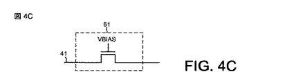
図4A〜Gは、本開示の例示の実施形態において、304や305などの変性インピーダンス要素として使用されることができる、入力リード線41を有する変性インピーダンス要素61の例示の回路図である。例示の一実施形態においては、変性インピーダンス要素61は、図4Aに示されるような抵抗と、図4Bに示されるようなキャパシタと、図4Cに示されるようなトランジスタと、図4Dに示されるような直列に結合された抵抗とキャパシタと、図4Eに示されるような直列に結合された抵抗とトランジスタと、図4Fに示されるような直列に結合されたキャパシタとトランジスタと、図4Gに示されるような直列に一緒に結合された抵抗とキャパシタとトランジスタと、を含むことができる。
4A-G are exemplary circuit diagrams of a modified
図5は、図3と一緒に本開示の例示の一方法を示すフローチャートである。プロセスは、ミキサ32aなどのミキサの利得状態が、プロセッサ323などによって決定されるブロック500において開始する。ミキサ32aは、25DCモードや50DCモードなど、複数のデューティサイクル(DC)モードを有する局部発振器(LO)システム300に結合される。次に、ブロック510において、デューティサイクルモードは、ミキサ32aの決定された利得状態に基づいてプロセッサ323などによって選択される。トランシーバシステム310が、ミキサ32aや32bなど、複数のミキサを含むコンフィギュレーションにおいては、デューティサイクルモードは、ミキサ32aや32bなどのミキサの決定された利得状態に基づいて選択される。例示の一実施形態においては、選択されたミキサ(単数または複数)の第1の利得状態は、高利得状態を備え、そして選択されたミキサ(単数または複数)の第2の利得は、低利得状態を備える。
FIG. 5 is a flowchart illustrating an exemplary method of the present disclosure in conjunction with FIG. The process begins at
次に、ブロック520において、局部発振器システム300は、ミキサ32aの決定された第1の利得状態に基づいて、選択された第1のデューティサイクルモードで動作するようにプロセッサ323などによって指示される。次に、ブロック530において、局部発振器システム300は、ミキサの決定された第2の利得状態に基づいて、選択された第2のデューティサイクルモードで動作するようにプロセッサ323などによって指示される。例示の一実施形態においては、第1のデューティサイクルは、それぞれ25DCや50DCなど、第2のデューティサイクルのデューティサイクルレートよりも低いデューティサイクルレートを備える。次いで、全部のフローは、終了する。
Next, at
図6は、例示の目的のためだけのSAWレスCDMAトランシーバシステム609との関連で説明される本開示の例示の一実施形態を示しているが、これは、同様に他の通信システムと共に使用されることもできる。図6に示されるように、トランシーバシステム609は、外部アンテナとすることができる、主要アンテナなどのアンテナ602に結合し、そして経路640などを経由して移動局モデム(MSM)620と通信している。MSM620は、MSM620の内部に、あるいは外部にあるようにすることができるメモリ622と通信しているプロセッサ623を備える。
FIG. 6 illustrates an exemplary embodiment of the present disclosure described in the context of a SAW-less
図6に示されるように、トランシーバシステム609は、直交(Q)信号などのRF信号をダウンコンバートするための、ミキサコア610や611など、2つ以上のミキサコアを有する、能動ミキサや受動ミキサなどのミキサ62aを含んでいる。RF信号は、先ずアンテナ602において、次いで低雑音増幅器(LNA)60の差動入力端子60aおよび60bへと受信され、この低雑音増幅器の出力リード線61aおよび61bは、次いでそれぞれミキサ62aの入力リード線613および612に結合される。例示の一実施形態においては、LNA60は、可変利得増幅器である。例示の一実施形態においては、ミキサコア610および611のうちの1つまたは複数は、スイッチングコアなど、能動コアまたは受動コアとすることができる。図6に示される例示の実施形態においては、ミキサ62aは、各々が、図3と一緒に説明される要素など、2つの交差結合スイッチング要素を有するギルバートミキサを備えるミキサコア610および611を有し、スイッチングコア610および611の前に利得ステージを有さない受動ミキサを備える。
As shown in FIG. 6, the
図6に示されるように、ミキサコア610および611の各々は、ミキサコア610についての入力リード線601および602や、ミキサコア611についての入力リード線603および604など、複数の入力リード線を有する。例示の一実施形態においては、ミキサ62aの入力612は、それぞれミキサコア610および611の入力リード線602および604に結合され、そしてミキサ62aの入力613は、それぞれミキサコア610および611の入力リード線601および603に結合される。ミキサ62aはまた、出力620aと620bとを含み、そしてミキサコア610および611の各々は、ミキサコア610についての出力601bおよび602bや、ミキサコア611についての出力603bおよび604bなど、1対の出力を有する。例示の一実施形態においては、ミキサ62aの出力620bは、それぞれミキサコア610および611の出力リード線602bおよび604bに結合され、そしてミキサ62aの出力620aは、それぞれミキサコア610および611の出力リード線601bおよび603bに結合される。
As shown in FIG. 6, each of the
次に、変性インピーダンス要素は、ミキサコア610の入力リード線601および602にそれぞれ結合される変性インピーダンス要素605および606や、ミキサコア611の入力リード線603および604にそれぞれ結合される変性インピーダンス要素607および608など、ミキサコア610および611の各々の入力リード線に結合される。変性インピーダンス要素605、606、607および608は、図に示されるように、ミキサコア610および611の内部に、あるいはそれぞれそれらの入力経路601a、602a、603aおよび604aに沿って外部に(図示されず)のいずれかで、入力リード線601、602、603および604にそれぞれ結合されることができる。
Next, the modified impedance elements are modified
ミキサ62aの中のミキサコアの数は、説明を簡単にするために2として選択されるが、ミキサ62aは、2つより多いミキサコアを有することができることに注意すべきである。例示の一実施形態においては、ミキサコアのうちの1つは、あらかじめ決定されたインピーダンス比だけなど、ミキサ62aの中の他のミキサコアとは異なるインピーダンス値のものである。例示の一実施形態においては、1つのミキサコアの変性インピーダンス要素は、あらかじめ決定されたインピーダンス比だけなど、他のミキサコアの変性インピーダンス要素に比べて異なっている。
It should be noted that the number of mixer cores in the
図6に示される例示の実施形態においては、ミキサコア610は、ミキサコア611に対するミキサコア610のあらかじめ決定されたインピーダンス比だけなど、ミキサコア611に比べて異なるインピーダンス値のものであり、ミキサコア610の変性インピーダンス要素605および606は、あらかじめ決定されたインピーダンス比だけなど、ミキサコア611の変性インピーダンス要素607および608に比べて異なるインピーダンス値のものである。例示の一実施形態においては、ミキサコア610は、ミキサコア611よりも大きな物理サイズを有することなどにより、ミキサコア611に対するミキサコア610のあらかじめ決定されたサイズ比だけなど、ミキサコア611より小さなインピーダンス値のものである。
In the exemplary embodiment shown in FIG. 6, the
例示の一実施形態においては、変性インピーダンス要素605、606、607および608の各々は、図4A〜Gと一緒に上記で説明されるように、抵抗と、キャパシタと、トランジスタと、直列に結合された抵抗とキャパシタと、直列に結合された抵抗とトランジスタと、直列に結合されたキャパシタとトランジスタと、直列に結合された抵抗とキャパシタとトランジスタと、から成ることができる。
In one exemplary embodiment, each of the modified
図6に示されるように、トランシーバシステム609は、先ずバッファ68にバッファされ、次いで、局部発振器(LO)システム600へと供給される前に、2分周のように周波数分周器67によって周波数分周されるダウンコンバートする電圧信号を生成するための電圧制御発振器69も含んでいる。局部発振器(LO)システム600は、ミキサ62aに供給されるLO信号を生成する複数のデューティサイクルモードを有する。局部発振器システム600は、ミキサ62aに対して、バッファされた信号を供給するバッファシステム66aに対する結合線75などを経由してLO信号を出力する、プログラマブルな25/50DCジェネレータなどのマルチモードデューティサイクル(DC)ジェネレータ66を含んでいる。例示の一実施形態においては、デューティサイクルジェネレータ66は、プログラマブルなデューティサイクルジェネレータである。
As shown in FIG. 6, the
図7と一緒により詳細に説明されるように、次いで、プロセッサ323などのコントローラは、(a)ミキサ62aの第1の利得に基づいて、25DCなど、第1のデューティサイクルモードで、ミキサコア611など、第1のミキサコアと、局部発振器システム600とを動作させるために、(b)ミキサ62aの第2の利得に基づいて、25DCなど、第1のデューティサイクルモードで、ミキサ62a、またはミキサコア610など第2のミキサコアのいずれかと、局部発振器システム600とを動作させるために、そして(c)ミキサ62aの第3の利得に基づいて、50DCなど、第2のデューティサイクルモードで、ミキサコア611など、第1のミキサコアと、局部発振器システム600とを動作させるために使用される。プロセッサ623などのコントローラからの指示(instructions)は、次いで指示されたデューティサイクルモードで動作することになるマルチモードデューティサイクル(DC)ジェネレータ66において受信される。
As described in more detail in conjunction with FIG. 7, the controller, such as
例示の一実施形態においては、バッファシステム66aは、結合線75などを経由して、デューティサイクルジェネレータシステム66の対応する出力リード線に結合された入力リード線を含んでいる。バッファシステム66aはまた、マルチモードデューティサイクル(DC)ジェネレータ66のデューティサイクルのうちの1つに対応するLO信号をミキサ62aに供給する、ミキサコア611の対応する入力リード線630aおよび630bに結合された第1の組の出力リード線63a1および63a2も含んでいる。バッファシステム66aはまた、マルチモードデューティサイクル(DC)ジェネレータ66のデューティサイクルのうちの1つに対応する信号をミキサ62aに供給する、ミキサコア610の入力リード線に結合された第2の組の出力リード線64a1および64a2も含んでいる。次いで、バッファされた信号は、出力620bおよび620aからそれぞれ出力されるダウンコンバートされた信号へと入力リード線612および613の中で受信されるRF信号についてダウンコンバートするために、それぞれミキサコア611および610のスイッチング要素に対して、対63a1、63a2と、64a1、64a2とによって供給される。
In one exemplary embodiment, the
例示の一実施形態においては、バッファシステム66aは、2つのサブバッファ(図示されず)を含んでおり、各サブバッファは、出力リード線63a1、63a2や、64a1、64a2など、バッファシステム66aの異なる対の出力リード線から出力する。例示の一実施形態においては、サブバッファは、異なるサイズのミキサコア610および611に対応する異なるサイズのものであり、そしてプロセッサ623などのコントローラからの制御線65aを経由して受信される制御信号に基づいて選択される。制御線65aを経由したサブバッファの選択は、選択されたサブバッファが、マルチモードデューティサイクル(DC)ジェネレータ66のデューティサイクルのうちの1つに対応するLO信号を対応するミキサコアに対して供給することを可能にするのに対して、他のミキサコアは、それらの対応するサブバッファからのLO信号を供給されない。例えば、ミキサコア610に対応するサブバッファが、選択される場合、選択されたサブバッファは、出力リード線64a1および64a2を経由して、ミキサコア610に対してLO信号を供給するが、LO信号は、他の選択されなかったサブバッファによっては出力リード線63a1および63a2を経由してミキサコア611に対して供給されることはない。
In one exemplary embodiment, the
図6に示されるように、トランシーバシステム609は、同相(I)信号など、追加の信号をダウンコンバートするための、ミキサ62bなど、追加のミキサを含むことができる。例示の一実施形態においては、ミキサ62bなど、追加の各ミキサはまた、上記で説明されるようにミキサ62aのような複数のミキサコアを有し、その各々は、それらの入力に結合された変性インピーダンス要素を有し、そしてまた、次いで両方のミキサ62aや62bなどのミキサの利得状態に基づいて動作する局部発振器システム600からLO信号を受信する。局部発振器システム600はまた、ミキサ62bについてのバッファシステム66bなど、追加のミキサについての追加のバッファシステムを有することになる。簡単にするために、トランシーバシステム609のオペレーションは、ミキサ62aとの関連だけでここにおいて詳細に説明されるが、複数のミキサを有するコンフィギュレーションにも簡単に適用されることができる。
As shown in FIG. 6, the
さらに、ミキサ62aや62bなど、各ミキサは、2つより多いミキサコアと、それらのバッファシステム66aおよび66bの中でそれぞれ異なるサイズの対応する数のサブバッファとを含むことができる。ミキサコンフィギュレーション当たりに複数のミキサと複数のミキサコアとを有する例示の一実施形態においては、局部発振器(LO)システム600は、ミキサに供給されるLO信号を生成する。以下で、そして図7と一緒により詳細に説明されるように、次いで、プロセッサ623などのコントローラは、(a)ミキサの第1の利得に基づいて第1のデューティサイクルモードで、ミキサの各々の中の対応する第1のミキサコアと、局部発振器システム600とを動作させ、(b)ミキサの第2の利得に基づいて第1のデューティサイクルモードで、ミキサ、またはミキサの各々の中の対応する第2のミキサコアと、局部発振器システム600とを動作させ、そして(c)ミキサの第3の利得に基づいて、第2のデューティサイクルモードで、ミキサの各々の中の対応する第1のミキサコアと、局部発振器システム600とを動作させる。
Further, each mixer, such as
図7は、図6と一緒に、本開示の別の例示の方法を示すフローチャートである。プロセスは、ミキサコア610や611など、複数のミキサコアを有し、そして25DCモードや50DCモードなど、複数のデューティサイクル(DC)モードを有する局部発振器(LO)600に結合される、ミキサ62aなどのミキサの利得状態が決定されるブロック700において開始する。決定された利得状態は、ミキサの第1の利得、第2の利得、または第3の利得に対応する。
FIG. 7, along with FIG. 6, is a flowchart illustrating another exemplary method of the present disclosure. The process includes a mixer, such as
例示の一実施形態においては、ミキサの第1の利得状態は、CDMA 1xレシーバにおける高利得低線形(high gain low-linearly)(G0LL)状態などの高利得状態を備え、ミキサの第2の利得は、CDMA 1xレシーバにおける低利得高線形(low gain high-linearly)(G0HL)状態などの低利得状態を備え、そして第3の利得状態は、CDMA 1xレシーバにおける低利得状態G1、G2、G3など、ミキサの第2の利得よりも低い低利得状態を備える。 In one exemplary embodiment, the first gain state of the mixer comprises a high gain state, such as a high gain low-linearly (G0LL) state in a CDMA 1x receiver, and the second gain of the mixer Has a low gain state, such as a low gain high-linearly (G0HL) state in a CDMA 1x receiver, and a third gain state is a low gain state G1, G2, G3, etc. in a CDMA 1x receiver A low gain state lower than the second gain of the mixer.
次に、ブロック710において、ミキサ62aなどのミキサの決定された利得状態に基づいて、ミキサコア610や611など、ミキサの中のミキサコアが、25DCモードや50DCモードなど、局部発振器システム600のデューティサイクルモードと同様に選択される。例示の一実施形態においては、ミキサコアとデューティサイクルとの選択は、プロセッサ623などのコントローラによって実行される。
Next, at
次に、ブロック720において、ミキサ62aなどのミキサが、CDMA 1xレシーバにおける高利得低線形(high gain low-linearly)(G0LL)状態など、第1の利得状態にあることが決定される場合、そのときには局部発振器システム600は、25DCなどの低デューティサイクルモードで動作するように、そしてミキサコア611などのミキサの選択されたミキサコアにLO信号を供給するように、プロセッサ623などのコントローラによって指示される。例示の一実施形態においては、ミキサコア611など、選択されたミキサコアは、ミキサコア610など、選択されていないミキサコアよりも大きなインピーダンス値を備える。プロセッサ623などのコントローラは、制御線65を経由してデューティサイクルジェネレータ66において受信される制御信号に基づいて25DCモードなど、低い方のデューティサイクルモードで動作するようにデューティサイクルジェネレータ66に指示する。プロセッサ623などのコントローラはまた、どのミキサコアが選択されるかに応じて、出力リード線64a1、64a2、または63a1、63a2のいずれかを経由することにより、選択されたミキサコアにLO信号を供給するように、制御線65aを経由してバッファシステム66aにおいて受信される制御信号に基づいて、バッファシステム66aに指示する。別の例示の実施形態においては、LO信号は、プロセッサ623などのコントローラからの指示に基づいて、ミキサコア610の入力601a、602a、630cおよび630dに対する経路に沿ってなど、1つまたは複数のミキサコアの1つまたは複数の入力に対する経路に沿って配置される1つまたは複数のマルチプレクサ(図示されず)を経由して、選択されたミキサコアへと供給される。
Next, if it is determined at
次に、ブロック730において、ミキサ62aなどのミキサが、CDMA 1xレシーバにおける低利得高線形(low gain high-linearly)(G0HL)状態など、第2の利得状態にあることが決定される場合、そのときには局部発振器システム600は、25DCなどの低デューティサイクルモードで動作するように、そして両方のミキサコア610と611とを選択することによりミキサ62aに対して、またはただ選択されたミキサコアだけに対してLO信号を供給するように、プロセッサ623などのコントローラによって指示される。例示の一実施形態においては、ミキサコア610など、選択されたミキサコアは、ミキサコア611など、選択されていないミキサコアよりも小さなインピーダンス値を備える。プロセッサ623などのコントローラは、制御線65を経由してデューティサイクルジェネレータ66において受信される制御信号に基づいて25DCモードなど、低い方のデューティサイクルモードで動作するように、デューティサイクルジェネレータ66に指示する。プロセッサ623などのコントローラはまた、どのミキサコアが選択されるかに応じて、出力リード線64a1、64a2、または63a1、63a2のいずれかを経由することにより、選択されたミキサコアに対して、あるいは両方のミキサコアが選択される場合には両方のミキサコアに対して、LO信号を供給するように、制御線65aを経由してバッファシステム66aにおいて受信される制御信号に基づいて、バッファシステム66aに指示する。別の例示の実施形態においては、LO信号は、プロセッサ623などのコントローラからの指示に基づいて、ミキサコア610の入力601a、602a、630cおよび630dに対する経路に沿ってなど、1つまたは複数のミキサコアの1つまたは複数の入力に対する経路に沿って配置される1つまたは複数のマルチプレクサ(図示されず)を経由して、選択されたミキサまたはミキサコアへと供給される。
Next, if it is determined at
次に、ブロック730において、ミキサ62aなどのミキサが、CDMA 1xレシーバにおける低利得状態G1、G2、G3など、第3の利得状態にあることが決定される場合、そのときには局部発振器システム600は、50DCなどのより高いデューティサイクルモードで動作するように、そして選択されたミキサコアにLO信号を供給するように、プロセッサ623などのコントローラによって指示される。例示の一実施形態においては、ミキサコア611など、選択されたミキサコアは、ミキサコア610など、選択されていないミキサコアよりも大きなインピーダンス値を備える。プロセッサ623などのコントローラは、制御線65を経由してデューティサイクルジェネレータ66において受信される制御信号に基づいて50DCモードなど、高い方のデューティサイクルモードで動作するようにデューティサイクルジェネレータ66に指示する。プロセッサ623などのコントローラはまた、どのミキサコアが選択されるかに応じて、出力リード線64a1、64a2、または63a1、63a2のいずれかを経由することにより、選択されたミキサコアにLO信号を供給するように、制御線65aを経由してバッファシステム66aにおいて受信される制御信号に基づいて、バッファシステム66aに指示する。別の例示の実施形態においては、LO信号は、プロセッサ623などのコントローラからの指示に基づいて、ミキサコア610の入力601a、602a、630cおよび630dに対する経路に沿ってなど、1つまたは複数のミキサコアの1つまたは複数の入力に対する経路に沿って配置される1つまたは複数のマルチプレクサ(図示されず)を経由して、選択されたミキサまたはミキサコアへと供給される。次いで、全体のフローは、終了する。
Next, at
50DC局部発振器に比べて、25DC局部発振器を有するレシーバは、LNAが同じ電流を消費する場合に、より高い利得を達成する。レシーバフロントエンドにおける、より高い利得は、RFレシーバにおいて、特にミキサのスイッチングコアの前に利得ステージなどのgm−セルを有さないSAWレスレシーバにおいて、よりよい雑音指数(NF)のために非常に望ましい。ほとんどのワイヤレス通信システムにおいては、最も厳しいNFは、高利得モードにおいてだけ必要とされる。他方、低利得モードは、最も電力が支配的なモードである。低利得モードにおける電力消費を低減させ、そして依然として緩和されたNFの仕様を満たすことは、RFレシーバをより電力効率の良いものにすることになる。先行技術より優れた本発明の実施形態の1つの利点は、高利得モードにおいて25DC LOを、そして低利得モードにおいて50DC LOを使用することにより、より大きな電力効率が、高利得モードについてのよりよいNFと同様に達成されることである。 Compared to a 50DC local oscillator, a receiver with a 25DC local oscillator achieves higher gain when the LNA consumes the same current. The higher gain at the receiver front end is very good for better noise figure (NF) in RF receivers, especially in SAW-less receivers that do not have a gm-cell such as a gain stage in front of the mixer switching core. desirable. In most wireless communication systems, the most stringent NF is only needed in the high gain mode. On the other hand, the low gain mode is the most power dominant mode. Reducing power consumption in the low gain mode and still meeting relaxed NF specifications will make the RF receiver more power efficient. One advantage of embodiments of the present invention over the prior art is that by using 25 DC LO in the high gain mode and 50 DC LO in the low gain mode, greater power efficiency is better for the high gain mode. It is achieved in the same way as NF.
様々な例示の実施形態は、例証の目的のために別々に論じられたが、それらは、別々に示された実施形態の特徴の一部または全部を有する1つの実施形態に組み合わされることができることに、注意すべきである。 Although various exemplary embodiments have been discussed separately for purposes of illustration, they can be combined into one embodiment having some or all of the features of the separately illustrated embodiments. You should be careful.
当業者(Those of skill in the art)は、情報および信号は、様々な異なる技術および技法のうちのどれを使用しても表されることができることを理解するであろう。例えば、上記説明全体を通して参照されることができるデータ、命令、コマンド、情報、信号、ビット、シンボル、およびチップは、電圧、電流、電磁波、磁気の場または粒子、光学的な場または粒子、あるいはそれらの任意の組合せによって表されることができる。当業者(Those of skill)は、さらに、ここにおける開示に関連して説明される様々な例示の論理ブロック、モジュール、回路、およびアルゴリズムステップは、電子のハードウェア、コンピュータソフトウェア、あるいは両方の組合せとしてインプリメントされることができることを理解するであろう。ハードウェアとソフトウェアとのこの交換可能性を明確に示すために、様々な例示のコンポーネント、ブロック、モジュール、回路、およびステップが、それらの機能の観点で上記に一般的に説明されている。そのような機能が、ハードウェアとしてインプリメントされるか、またはソフトウェアとしてインプリメントされるかは、全体的なシステムに課される特定のアプリケーションおよび設計の制約条件に依存する。当業者(Skilled artisans)は、特定の各アプリケーションについて変化するやり方で、説明された機能をインプリメントすることができるが、そのようなインプリメンテーションの決定は、本開示の範囲からの逸脱(departure)を引き起こすものとしては解釈されるべきではない。 Those of ordinary skill in the art will understand that information and signals can be represented using any of a variety of different technologies and techniques. For example, data, instructions, commands, information, signals, bits, symbols, and chips that can be referenced throughout the above description are voltages, currents, electromagnetic waves, magnetic fields or particles, optical fields or particles, or It can be represented by any combination thereof. Those of skill in the art will further note that the various exemplary logic blocks, modules, circuits, and algorithm steps described in connection with the disclosure herein may be implemented as electronic hardware, computer software, or a combination of both. It will be understood that it can be implemented. To clearly illustrate this interchangeability between hardware and software, various illustrative components, blocks, modules, circuits, and steps have been described above generally in terms of their functionality. Whether such functionality is implemented as hardware or software depends upon the particular application and design constraints imposed on the overall system. Skilled artisans can implement the described functionality in a varying manner for each particular application, but such implementation decisions are a departure from the scope of this disclosure. Should not be interpreted as causing
ここにおける開示に関連して説明される様々な例示の論理ブロック、モジュール、および回路は、ここにおいて説明される機能を実行するように設計された汎用プロセッサ、デジタル信号プロセッサ(digital signal processor)(DSP)、特定用途向け集積回路(application specific integrated circuit)(ASIC)、フィールドプログラマブルゲートアレイ(field programmable gate array)(FPGA)または他のプログラマブルロジックデバイス、ディスクリートなゲートまたはトランジスタのロジック、ディスクリートハードウェアコンポーネント(discrete hardware components)、あるいはそれらの任意の組合せを用いてインプリメントされ、または実行されることができる。汎用プロセッサは、マイクロプロセッサであってもよいが、代替案においては、プロセッサは、従来の任意のプロセッサ、コントローラ、マイクロコントローラ、または状態機械であってもよい。プロセッサは、コンピューティングデバイスの組合せ、例えば、DSPとマイクロプロセッサとの組合せ、複数のマイクロプロセッサ、DSPコアと組み合わされた1つまたは複数のマイクロプロセッサ、あるいは他のそのような任意のコンフィギュレーションとしてインプリメントされることもできる。 Various exemplary logic blocks, modules, and circuits described in connection with the disclosure herein are general purpose processors, digital signal processors (DSPs) that are designed to perform the functions described herein. ), Application specific integrated circuit (ASIC), field programmable gate array (FPGA) or other programmable logic device, discrete gate or transistor logic, discrete hardware components ( discrete hardware components), or any combination thereof, can be implemented or implemented. A general purpose processor may be a microprocessor, but in the alternative, the processor may be any conventional processor, controller, microcontroller, or state machine. The processor is implemented as a combination of computing devices, eg, a DSP and microprocessor combination, multiple microprocessors, one or more microprocessors combined with a DSP core, or any other such configuration. Can also be done.
ここにおける開示に関連して説明される方法またはアルゴリズムのステップは、ハードウェアの形で直接に、プロセッサによって実行されるソフトウェアモジュールの形で、あるいはそれらの2つの組合せの形で実施されることができる。ソフトウェアモジュールは、RAMメモリ、フラッシュメモリ、ROMメモリ、EPROMメモリ、EEPROMメモリ、レジスタ、ハードディスク、リムーバブルディスク、CD−ROM、または当技術分野において知られている他の任意の形態のストレージ媒体の中に存在することができる。例示のストレージ媒体は、プロセッサが、ストレージ媒体から情報を読み取り、そしてストレージ媒体に情報を書き込むことができるように、プロセッサに結合される。代替案においては、ストレージ媒体は、プロセッサと一体化していることもできる。プロセッサとストレージ媒体とは、ASICの中に存在することができる。ASICは、ユーザ端末の中に存在することができる。代替案においては、プロセッサとストレージ媒体とは、ユーザ端末の中にディスクリートコンポーネントとして存在することもできる。 The method or algorithm steps described in connection with the disclosure herein may be implemented directly in hardware, in software modules executed by a processor, or in a combination of the two. it can. The software module is in RAM memory, flash memory, ROM memory, EPROM memory, EEPROM memory, registers, hard disk, removable disk, CD-ROM, or any other form of storage medium known in the art. Can exist. An exemplary storage medium is coupled to the processor such that the processor can read information from, and write information to, the storage medium. In the alternative, the storage medium may be integral to the processor. The processor and the storage medium can reside in an ASIC. The ASIC can exist in the user terminal. In the alternative, the processor and the storage medium may reside as discrete components in a user terminal.
上記で説明される方法は、コンピュータに、上記で説明されたプロセスを実行するようにさせるためのコードを有するコンピュータ可読媒体を有するコンピュータプログラムプロダクト(computer program product)の形でインプリメントされることができることに注意すべきである。1つまたは複数の例示の実施形態においては、説明される機能は、ハードウェア、ソフトウェア、ファームウェア、またはそれらの任意の組合せの形でインプリメントされることができる。ソフトウェアの形でインプリメントされる場合、それらの機能は、コンピュータ可読媒体上に1つまたは複数の命令またはコードとして記憶され、あるいはその上で送信されることができる。コンピュータ可読媒体は、ある場所から別の場所へのコンピュータプログラムの転送を容易にする任意の媒体を含めて、コンピュータストレージ媒体と、通信媒体との両方を含んでいる。ストレージ媒体は、汎用または専用のコンピュータによってアクセスされることができる使用可能な任意の媒体とすることができる。例として、限定するものではないが、そのようなコンピュータ可読媒体は、RAM、ROM、EEPROM、CD−ROMまたは他の光ディスクストレージ、磁気ディスクストレージまたは他の磁気ストレージデバイス、あるいは命令またはデータ構造の形態で望ましいプログラムコード手段を搬送し、または記憶するために使用されることができ、そして汎用または専用のコンピュータ、あるいは汎用または専用のプロセッサによってアクセスされることができる他の任意の媒体、を備えることができる。また、任意の接続は、コンピュータ可読媒体と適切に名づけられることもある。例えば、ソフトウェアが、同軸ケーブル、光ファイバケーブル、ツイストペア(twisted pair)、デジタル加入者回線(DSL)、または赤外線、無線、マイクロ波などのワイヤレス技術を使用して、ウェブサイト、サーバ、または他のリモートソースから送信される場合、そのときには同軸ケーブル、光ファイバケーブル、ツイストペア、DSL、または赤外線、無線、マイクロ波などのワイヤレス技術は、媒体の定義の中に含まれる。ここにおいて使用されるようなディスク(Disk)およびディスク(disc)は、コンパクトディスク(compact disc)(CD)、レーザーディスク(登録商標)(laser disc)、光ディスク(optical disc)、デジタル多用途ディスク(digital versatile disc)(DVD)、フロッピー(登録商標)ディスク、およびブルーレイディスク(blu-ray disc)を含み、ここでディスク(disks)は通常、データを磁気的に再生するが、ディスク(discs)は、レーザを用いて光学的にデータを再生する。上記の組合せもまた、コンピュータ可読媒体の範囲内に含められるべきである。 The method described above can be implemented in the form of a computer program product having a computer readable medium having code for causing a computer to perform the process described above. Should be noted. In one or more exemplary embodiments, the functions described can be implemented in hardware, software, firmware, or any combination thereof. If implemented in software, the functions can be stored on or transmitted over as one or more instructions or code on a computer-readable medium. Computer-readable media includes both computer storage media and communication media including any medium that facilitates transfer of a computer program from one place to another. A storage media may be any available media that can be accessed by a general purpose or special purpose computer. By way of example, and not limitation, such computer readable media can be RAM, ROM, EEPROM, CD-ROM or other optical disk storage, magnetic disk storage or other magnetic storage device, or in the form of instructions or data structures. Comprising any general-purpose or special-purpose computer or any other medium that can be accessed by a general-purpose or special-purpose processor Can do. Any connection may also be appropriately named a computer-readable medium. For example, software may use a coaxial cable, fiber optic cable, twisted pair, digital subscriber line (DSL), or wireless technology such as infrared, radio, microwave, etc. When transmitted from a remote source, then coaxial cable, fiber optic cable, twisted pair, DSL, or wireless technologies such as infrared, radio, microwave are included in the definition of the medium. Discs and discs as used herein include compact discs (CD), laser discs, laser discs, optical discs, digital versatile discs ( digital versatile discs (DVDs), floppy disks, and blu-ray discs, where disks normally play data magnetically, but discs are The data is optically reproduced using a laser. Combinations of the above should also be included within the scope of computer-readable media.
本開示の先の説明は、任意の当業者が、本開示を作りまたは使用することを可能にするために提供される。本開示に対する様々な修正は、当業者には簡単に明らかになり、そしてここにおいて定義される包括的な原理は、本開示の範囲から逸脱することなく、他の変形にも適用されることができる。したがって、本開示は、ここにおいて説明される例および設計だけに限定されるようには意図されず、ここにおいて開示される原理および新規の特徴と整合した最も広い範囲を与えられるべきである。 The previous description of the disclosure is provided to enable any person skilled in the art to make or use the disclosure. Various modifications to the present disclosure will be readily apparent to those skilled in the art, and the generic principles defined herein may be applied to other variations without departing from the scope of the present disclosure. it can. Accordingly, this disclosure is not intended to be limited to only the examples and designs described herein, but is to be accorded the widest scope consistent with the principles and novel features disclosed herein.
Claims (25)
前記ミキサの第1の入力リード線に結合された第1の変性インピーダンス要素と、
前記ミキサの第2の入力リード線に結合された第2の変性インピーダンス要素と、
前記ミキサのためのLO信号を生成する、複数のデューティサイクルモードを備える局部発振器(LO)システムと、
を備え、前記局部発振器システムは、前記ミキサの第1の利得状態に基づいて第1のデューティサイクルで、そして前記ミキサの第2の利得状態に基づいて第2のデューティサイクルで、動作する、装置。 A mixer having a plurality of input leads;
A first modified impedance element coupled to a first input lead of the mixer;
A second modified impedance element coupled to a second input lead of the mixer;
A local oscillator (LO) system with a plurality of duty cycle modes that generates an LO signal for the mixer;
And wherein the local oscillator system operates at a first duty cycle based on a first gain state of the mixer and at a second duty cycle based on a second gain state of the mixer .
前記ミキサの前記決定された利得状態に基づいて前記局部発振器システムの前記複数のデューティサイクルモードからデューティサイクルモードを選択することと、
前記ミキサの決定された第1の利得状態に基づいて、選択された第1のデューティサイクルモードで動作するように前記局部発振器システムに指示することと、
前記ミキサの決定された第2の利得状態に基づいて、選択された第2のデューティサイクルモードで動作するように前記局部発振器システムに指示することと、
を備える方法。 Determining a gain state of a mixer coupled to a local oscillator (LO) having a plurality of duty cycle modes, wherein the determined gain state is at least one of the first and second gains of the mixer Corresponding to
Selecting a duty cycle mode from the plurality of duty cycle modes of the local oscillator system based on the determined gain state of the mixer;
Instructing the local oscillator system to operate in a selected first duty cycle mode based on the determined first gain state of the mixer;
Instructing the local oscillator system to operate in a selected second duty cycle mode based on the determined second gain state of the mixer;
A method comprising:
前記コンピュータに、前記ミキサの前記決定された利得状態に基づいて前記局部発振器システムの前記複数のデューティサイクルモードからデューティサイクルモードを選択するようにさせるためのコードと、
前記コンピュータに、前記ミキサの決定された第1の利得状態に基づいて、選択された第1のデューティサイクルモードで動作するように前記局部発振器システムに指示するようにさせるためのコードと、
前記コンピュータに、前記ミキサの決定された第2の利得状態に基づいて、選択された第2のデューティサイクルモードで動作するように前記局部発振器システムに指示するようにさせるためのコードと、
を備えるコンピュータ可読媒体、
を備えるコンピュータプログラムプロダクト。 A code for causing a computer to determine a gain state of a mixer coupled to a local oscillator (LO) having a plurality of duty cycle modes, and wherein the determined gain state is the first and second of the mixer. Corresponding to at least one of the two gains,
Code for causing the computer to select a duty cycle mode from the plurality of duty cycle modes of the local oscillator system based on the determined gain state of the mixer;
Code for causing the computer to instruct the local oscillator system to operate in a selected first duty cycle mode based on the determined first gain state of the mixer;
Code for causing the computer to instruct the local oscillator system to operate in a selected second duty cycle mode based on the determined second gain state of the mixer;
A computer-readable medium comprising:
A computer program product comprising:
前記ミキサの前記決定された利得状態に基づいて前記局部発振器システムの前記複数のデューティサイクルモードからデューティサイクルモードを選択するための手段と、
前記ミキサの決定された第1の利得状態に基づいて、選択された第1のデューティサイクルモードで動作するように、そして前記ミキサの決定された第2の利得状態に基づいて、選択された第2のデューティサイクルモードで動作するように、前記局部発振器システムに指示するための手段と、
を備える装置。 Means for determining a gain state of a mixer coupled to a local oscillator (LO) having a plurality of duty cycle modes, and wherein the determined gain state is the first and second gains of the mixer Corresponding to at least one,
Means for selecting a duty cycle mode from the plurality of duty cycle modes of the local oscillator system based on the determined gain state of the mixer;
Based on the determined first gain state of the mixer, to operate in the selected first duty cycle mode and based on the determined second gain state of the mixer Means for instructing the local oscillator system to operate in a two duty cycle mode;
A device comprising:
前記ミキサに供給されるLO信号を生成する、複数のデューティサイクルモードを備える局部発振器(LO)システムと、
(a)前記ミキサの第1の利得に基づいて第1のデューティサイクルモードで、前記複数のミキサコアからの第1のミキサコアと、前記局部発振器システムとを動作させ、(b)前記ミキサの第2の利得に基づいて前記第1のデューティサイクルモードで、前記ミキサと、前記複数のミキサコアからの第2のミキサコアとのうちの少なくとも一方と、前記局部発振器システムとを動作させ、そして(c)前記ミキサの第3の利得に基づいて第2のデューティサイクルモードで、前記第1のミキサコアと、前記局部発振器システムとを動作させるコントローラと、
を備える装置。 A mixer comprising a plurality of mixer cores;
A local oscillator (LO) system with a plurality of duty cycle modes that generates an LO signal supplied to the mixer;
(A) operating a first mixer core from the plurality of mixer cores and the local oscillator system in a first duty cycle mode based on a first gain of the mixer; and (b) a second of the mixer. Operating at least one of the mixer, a second mixer core from the plurality of mixer cores, and the local oscillator system in the first duty cycle mode based on a gain of A controller for operating the first mixer core and the local oscillator system in a second duty cycle mode based on a third gain of the mixer;
A device comprising:
をさらに備える請求項9の装置。 A low noise amplifier (LNA), each having a plurality of output leads coupled to corresponding input leads of the mixer,
10. The apparatus of claim 9, further comprising:
各々が、前記デューティサイクルジェネレータシステムの前記複数の出力リード線の中の対応する出力リード線に結合された複数の入力リード線と、
前記コントローラから受信される制御信号に基づいて前記の第1および第2のデューティサイクルのうちの少なくとも一方に対応する信号を前記ミキサに供給する、前記ミキサの前記第1のミキサコアの対応する第1の複数の入力リード線に結合された第1の複数の出力リード線と、
前記コントローラから受信される制御信号に基づいて前記の第1および第2のデューティサイクルのうちの少なくとも一方に対応する信号を前記ミキサに供給する、前記ミキサの前記第2のミキサコアの対応する第2の複数の入力リード線に結合された第2の複数の出力リード線と、
を備えるバッファシステムをさらに備える、請求項19の装置。 The local oscillator (LO) system is:
A plurality of input leads each coupled to a corresponding output lead among the plurality of output leads of the duty cycle generator system;
A corresponding first of the first mixer cores of the mixer that supplies the mixer with a signal corresponding to at least one of the first and second duty cycles based on a control signal received from the controller. A first plurality of output leads coupled to the plurality of input leads;
A corresponding second of the second mixer core of the mixer that supplies the mixer with a signal corresponding to at least one of the first and second duty cycles based on a control signal received from the controller; A second plurality of output leads coupled to the plurality of input leads;
20. The apparatus of claim 19, further comprising a buffer system comprising:
前記ミキサの前記決定された利得状態に基づいて、前記複数のミキサコアからのミキサコアと、前記局部発振器システムの前記複数のデューティサイクルモードからのデューティサイクルモードとを選択することと、
前記ミキサが、前記第1の利得状態にあることが決定される場合に、選択された第1のデューティサイクルモードで動作するように、そして選択された第1のミキサコアにLO信号を供給するように、前記局部発振器システムに指示することと、
前記ミキサが、前記第2の利得状態にあることが決定される場合に、前記選択された第1のデューティサイクルモードで動作するように、そして前記ミキサと、選択された第2のミキサコアとのうちの少なくとも一方にLO信号を供給するように、前記局部発振器システムに指示することと、
前記ミキサが、前記第3の利得状態にあることが決定される場合に、選択された第2のデューティサイクルモードで動作するように、そして前記選択された第1のミキサコアにLO信号を供給するように、前記局部発振器システムに指示することと、
を備える方法。 Determining a gain state of a mixer having a plurality of mixer cores and coupled to a local oscillator (LO) having a plurality of duty cycle modes, wherein the determined gain state is a first, a second, Corresponding to at least one of 2, and a third gain,
Selecting a mixer core from the plurality of mixer cores and a duty cycle mode from the plurality of duty cycle modes of the local oscillator system based on the determined gain state of the mixer;
When it is determined that the mixer is in the first gain state, to operate in a selected first duty cycle mode and to supply a LO signal to the selected first mixer core Instructing the local oscillator system;
When it is determined that the mixer is in the second gain state, to operate in the selected first duty cycle mode and between the mixer and the selected second mixer core Instructing the local oscillator system to provide an LO signal to at least one of them;
If it is determined that the mixer is in the third gain state, operate in a selected second duty cycle mode and provide an LO signal to the selected first mixer core Instructing the local oscillator system to:
A method comprising:
前記コンピュータに、前記ミキサの前記決定された利得状態に基づいて、前記複数のミキサコアからのミキサコアと、前記局部発振器システムの前記複数のデューティサイクルモードからのデューティサイクルモードとを選択するようにさせるためのコードと、
前記コンピュータに、前記ミキサが、前記第1の利得状態にあることが決定される場合に、選択された第1のデューティサイクルモードで動作するように、そして選択された第1のミキサコアにLO信号を供給するように、前記局部発振器システムに指示するようにさせるためのコードと、
前記コンピュータに、前記ミキサが、前記第2の利得状態にあることが決定される場合に、前記選択された第1のデューティサイクルモードで動作するように、そして前記ミキサと、選択された第2のミキサコアとのうちの少なくとも一方にLO信号を供給するように、前記局部発振器システムに指示するようにさせるためのコードと、
前記コンピュータに、前記ミキサが、前記第3の利得状態にあることが決定される場合に、選択された第2のデューティサイクルモードで動作するように、そして前記選択された第1のミキサコアにLO信号を供給するように、前記局部発振器システムに指示するようにさせるためのコードと、
を備えるコンピュータ可読媒体、
を備えるコンピュータプログラムプロダクト。 Code for causing a computer to determine a gain state of a mixer coupled to a local oscillator (LO) having a plurality of mixer cores and having a plurality of duty cycle modes, and wherein the determined gain state is Corresponding to at least one of the first, second, and third gains of the mixer,
To cause the computer to select a mixer core from the plurality of mixer cores and a duty cycle mode from the plurality of duty cycle modes of the local oscillator system based on the determined gain state of the mixer And the code
An LO signal is sent to the computer to operate in the selected first duty cycle mode when the mixer is determined to be in the first gain state and to the selected first mixer core. A code for instructing the local oscillator system to supply
The computer is configured to operate in the selected first duty cycle mode when the mixer is determined to be in the second gain state, and the mixer and the selected second A code for instructing the local oscillator system to provide an LO signal to at least one of the mixer cores;
The computer is configured to operate in a selected second duty cycle mode when the mixer is determined to be in the third gain state, and to the selected first mixer core. A code for instructing the local oscillator system to provide a signal;
A computer-readable medium comprising:
A computer program product comprising:
前記ミキサの前記決定された利得状態に基づいて、前記複数のミキサコアからのミキサコアと、前記局部発振器システムの前記複数のデューティサイクルモードからのデューティサイクルモードとを選択するための手段と、
前記ミキサが、前記第1の利得状態にあることが決定される場合に、選択された第1のデューティサイクルモードで動作するように、そして選択された第1のミキサコアにLO信号を供給するように、前記ミキサが、前記第2の利得状態にあることが決定される場合に、前記選択された第1のデューティサイクルモードで動作するように、そして前記ミキサと、選択された第2のミキサコアとのうちの少なくとも一方にLO信号を供給するように、そして前記ミキサが、前記第3の利得状態にあることが決定される場合に、選択された第2のデューティサイクルモードで動作するように、そして前記選択された第1のミキサコアにLO信号を供給するように、前記局部発振器システムに指示するための手段と、
を備える装置。 Means for determining a gain state of a mixer coupled to a local oscillator (LO) having a plurality of mixer cores and having a plurality of duty cycle modes, wherein the determined gain state is a first value of the mixer. Corresponding to at least one of the second, third and third gains,
Means for selecting a mixer core from the plurality of mixer cores and a duty cycle mode from the plurality of duty cycle modes of the local oscillator system based on the determined gain state of the mixer;
When it is determined that the mixer is in the first gain state, to operate in a selected first duty cycle mode and to supply a LO signal to the selected first mixer core And when the mixer is determined to be in the second gain state, so as to operate in the selected first duty cycle mode, and the mixer and the selected second mixer core And supplying a LO signal to at least one of the and the mixer to operate in the selected second duty cycle mode when it is determined that the mixer is in the third gain state. And means for instructing the local oscillator system to provide an LO signal to the selected first mixer core;
A device comprising:
Applications Claiming Priority (3)
| Application Number | Priority Date | Filing Date | Title |
|---|---|---|---|
| US12/052,657 | 2008-03-20 | ||
| US12/052,657 US8639205B2 (en) | 2008-03-20 | 2008-03-20 | Reduced power-consumption receivers |
| PCT/US2009/037884 WO2009117707A1 (en) | 2008-03-20 | 2009-03-20 | Reduced power-consumption receivers |
Related Child Applications (1)
| Application Number | Title | Priority Date | Filing Date |
|---|---|---|---|
| JP2013150974A Division JP2013255255A (en) | 2008-03-20 | 2013-07-19 | Reduced power-consumption receivers |
Publications (1)
| Publication Number | Publication Date |
|---|---|
| JP2011515967A true JP2011515967A (en) | 2011-05-19 |
Family
ID=40673293
Family Applications (2)
| Application Number | Title | Priority Date | Filing Date |
|---|---|---|---|
| JP2011501001A Ceased JP2011515967A (en) | 2008-03-20 | 2009-03-20 | Reduced power consumption receiver |
| JP2013150974A Pending JP2013255255A (en) | 2008-03-20 | 2013-07-19 | Reduced power-consumption receivers |
Family Applications After (1)
| Application Number | Title | Priority Date | Filing Date |
|---|---|---|---|
| JP2013150974A Pending JP2013255255A (en) | 2008-03-20 | 2013-07-19 | Reduced power-consumption receivers |
Country Status (7)
| Country | Link |
|---|---|
| US (2) | US8639205B2 (en) |
| EP (1) | EP2279565A1 (en) |
| JP (2) | JP2011515967A (en) |
| KR (1) | KR101157438B1 (en) |
| CN (1) | CN102037655A (en) |
| TW (1) | TW201001936A (en) |
| WO (1) | WO2009117707A1 (en) |
Families Citing this family (15)
| Publication number | Priority date | Publication date | Assignee | Title |
|---|---|---|---|---|
| US8019310B2 (en) * | 2007-10-30 | 2011-09-13 | Qualcomm Incorporated | Local oscillator buffer and mixer having adjustable size |
| US8929840B2 (en) * | 2007-09-14 | 2015-01-06 | Qualcomm Incorporated | Local oscillator buffer and mixer having adjustable size |
| US8599938B2 (en) | 2007-09-14 | 2013-12-03 | Qualcomm Incorporated | Linear and polar dual mode transmitter circuit |
| US7899426B2 (en) * | 2007-10-30 | 2011-03-01 | Qualcomm Incorporated | Degenerated passive mixer in saw-less receiver |
| US9735734B2 (en) * | 2008-10-01 | 2017-08-15 | Telefonaktiebolaget Lm Ericsson (Publ) | Re-configurable passive mixer for wireless receivers |
| JP2010147988A (en) * | 2008-12-22 | 2010-07-01 | Toshiba Corp | Amplifier circuit and radio receiver |
| US9093956B2 (en) * | 2011-11-04 | 2015-07-28 | Broadcom Corporation | Variable duty-cycle multi-standard mixer |
| CN104541553B (en) * | 2012-06-20 | 2018-07-13 | 瑞典爱立信有限公司 | Method and apparatus for radio resource control |
| US8787854B2 (en) | 2012-07-25 | 2014-07-22 | Qualcomm Incorporated | Low power local oscillator signal generation |
| KR102268110B1 (en) * | 2014-08-05 | 2021-06-22 | 삼성전자주식회사 | Method and apparatus for modulating data and medium thereof |
| US9748993B2 (en) * | 2015-09-08 | 2017-08-29 | Mediatek Inc. | Radio frequency receiver front-end with gain control capability as well as improved impedance matching control capability |
| US9680461B1 (en) * | 2016-03-01 | 2017-06-13 | Cognitive Systems Corp. | Generating local oscillator signals in a wireless sensor device |
| EP3759845B1 (en) * | 2018-02-28 | 2024-05-01 | BAE SYSTEMS Information and Electronic Systems Integration Inc. | Power efficient radio mixers |
| KR102608378B1 (en) * | 2019-06-18 | 2023-12-01 | 삼성전자주식회사 | Structure of electronic device for optimizing performance of antenna and method thereof |
| US11277108B1 (en) * | 2020-12-28 | 2022-03-15 | Analog Devices International Unlimited Company | Variable gain amplifiers with cross-couple switching arrangements |
Citations (4)
| Publication number | Priority date | Publication date | Assignee | Title |
|---|---|---|---|---|
| EP0276130A2 (en) * | 1987-01-23 | 1988-07-27 | THE GENERAL ELECTRIC COMPANY, p.l.c. | Electrical signal mixer circuits |
| JP2000022575A (en) * | 1998-07-01 | 2000-01-21 | Nec Corp | Receiver and storage medium with program |
| WO2008008759A2 (en) * | 2006-07-11 | 2008-01-17 | Qualcomm Incorporated | Systems, methods, and apparatus for frequency conversion |
| JP2008160327A (en) * | 2006-12-21 | 2008-07-10 | Kyocera Corp | Receiver and receiving method |
Family Cites Families (112)
| Publication number | Priority date | Publication date | Assignee | Title |
|---|---|---|---|---|
| US3212024A (en) | 1961-01-13 | 1965-10-12 | Aircraft Radio Corp | Measuring and testing circuit for frequency synthesizer |
| US3212027A (en) | 1961-10-20 | 1965-10-12 | Research Corp | Tunnel diode frequency modulator and transmitter system |
| JPH05343923A (en) * | 1992-06-08 | 1993-12-24 | Matsushita Electric Ind Co Ltd | Semiconductor device |
| JPH0748964B2 (en) | 1992-12-02 | 1995-05-31 | 岩手県 | Bioreactor |
| US5525937A (en) | 1992-12-28 | 1996-06-11 | Sony Corporation | Frequency conversion circuit with UHF/VHF common PLL buffer |
| GB9316869D0 (en) | 1993-08-13 | 1993-09-29 | Philips Electronics Uk Ltd | Transmitter and power amplifier therefor |
| JPH07202677A (en) | 1993-12-27 | 1995-08-04 | Nippon Telegr & Teleph Corp <Ntt> | Cmos output buffer circuit |
| CN1087120C (en) | 1994-11-10 | 2002-07-03 | 松下电器产业株式会社 | Direct frequency conversion receiver |
| US6147543A (en) | 1996-01-19 | 2000-11-14 | Motorola, Inc. | Method and apparatus for selecting from multiple mixers |
| JPH09261102A (en) | 1996-03-22 | 1997-10-03 | Toshiba Corp | Amplitude correction circuit |
| JPH09261106A (en) | 1996-03-22 | 1997-10-03 | Matsushita Electric Ind Co Ltd | Mobile radio equipment operated for plural frequency bands |
| TW331681B (en) | 1997-02-18 | 1998-05-11 | Chyng-Guang Juang | Wide-band low-noise low-crossover distortion receiver |
| US6016422A (en) | 1997-10-31 | 2000-01-18 | Motorola, Inc. | Method of and apparatus for generating radio frequency quadrature LO signals for direct conversion transceivers |
| JP3568102B2 (en) * | 1998-07-24 | 2004-09-22 | 松下電器産業株式会社 | Direct conversion receiver |
| DE69920273T2 (en) | 1998-11-12 | 2005-09-22 | Broadcom Corp., Irvine | INTEGRATED TUNER ARCHITECTURE |
| US6584090B1 (en) | 1999-04-23 | 2003-06-24 | Skyworks Solutions, Inc. | System and process for shared functional block CDMA and GSM communication transceivers |
| US6307894B2 (en) | 1999-05-25 | 2001-10-23 | Conexant Systems, Inc. | Power amplification using a direct-upconverting quadrature mixer topology |
| US6266517B1 (en) | 1999-12-30 | 2001-07-24 | Motorola, Inc. | Method and apparatus for correcting distortion in a transmitter |
| US6871057B2 (en) * | 2000-03-08 | 2005-03-22 | Nippon Telegraph And Telephone Corporation | Mixer circuit |
| FI108584B (en) | 2000-03-24 | 2002-02-15 | Nokia Corp | Method for generating an intermediate frequency signal in a mixer and a mixer |
| US7139547B2 (en) | 2000-11-29 | 2006-11-21 | Broadcom Corporation | Integrated direct conversion satellite tuner |
| JP3970623B2 (en) | 2001-02-28 | 2007-09-05 | シャープ株式会社 | Variable gain amplifier |
| JP3721144B2 (en) | 2001-05-11 | 2005-11-30 | 株式会社東芝 | Frequency converter, quadrature demodulator and quadrature modulator |
| DE10132587A1 (en) | 2001-07-05 | 2002-11-14 | Infineon Technologies Ag | Transmission device with power control e.g. for RF systems, has output of DAC coupled to modulator for modulating carrier signal with useful signal to be sent |
| US6487398B1 (en) | 2001-08-14 | 2002-11-26 | Motorola, Inc. | Low noise architecture for a direct conversion transmitter |
| JP2003188754A (en) | 2001-12-14 | 2003-07-04 | Hitachi Ltd | Local oscillation frequency signal output circuit and portable terminal using the same |
| FR2836305B1 (en) | 2002-02-15 | 2004-05-07 | St Microelectronics Sa | AB CLASS DIFFERENTIAL MIXER |
| US6590438B1 (en) | 2002-03-08 | 2003-07-08 | Sirific Wireless Corporation | Integrated circuit adjustable RF mixer |
| JP2003283361A (en) | 2002-03-22 | 2003-10-03 | Matsushita Electric Ind Co Ltd | Radio reception device, radio reception method, program, and medium |
| JP2003298441A (en) | 2002-04-01 | 2003-10-17 | Hitachi Ltd | Low power consumption receiver |
| US6906996B2 (en) | 2002-05-20 | 2005-06-14 | Qualcomm Inc | Multiple modulation wireless transmitter |
| JP3979237B2 (en) | 2002-09-05 | 2007-09-19 | 株式会社日立製作所 | Wireless communication device and high-frequency integrated circuit used therefor |
| US7184491B2 (en) | 2002-09-05 | 2007-02-27 | Htachi, Ltd. | Wireless communication apparatus |
| TW566011B (en) | 2002-09-23 | 2003-12-11 | Ind Tech Res Inst | Dual mode receiving method and device |
| JP4212557B2 (en) | 2002-12-20 | 2009-01-21 | 株式会社ルネサステクノロジ | Transmission circuit and transceiver using the same |
| US20040127172A1 (en) | 2002-12-27 | 2004-07-01 | Agere Systems Inc. | Phase-error suppressor and a method of suppressing phase-error |
| JP3095242U (en) * | 2003-01-14 | 2003-07-25 | アルプス電気株式会社 | Television tuner |
| JP3824610B2 (en) | 2003-03-05 | 2006-09-20 | 松下電器産業株式会社 | Transmitter circuit |
| US7102411B2 (en) | 2003-03-06 | 2006-09-05 | Broadcom Corporation | High linearity passive mixer and associated LO buffer |
| US7027833B1 (en) | 2003-04-03 | 2006-04-11 | The United States Of America As Represented By The Secretary Of The Navy | Dual band superheterodyne receiver |
| US6985033B1 (en) | 2003-05-15 | 2006-01-10 | Marvell International Ltd. | Circuits and methods for adjusting power amplifier predistortion, and power amplifiers and other devices including the same |
| US7209727B2 (en) | 2003-06-12 | 2007-04-24 | Broadcom Corporation | Integrated circuit radio front-end architecture and applications thereof |
| US7120413B2 (en) * | 2003-06-22 | 2006-10-10 | Realtek Semiconductor Corp. | Television tuner and method of processing a received RF signal |
| JP3844352B2 (en) | 2003-08-07 | 2006-11-08 | 松下電器産業株式会社 | Transmitter |
| WO2005027339A1 (en) * | 2003-09-16 | 2005-03-24 | Koninklijke Philips Electronics N.V., | Mixer circuit, receiver comprising a mixer circuit, method for generating an output signal by mixing an input signal with an oscillator signal |
| EP1521376B1 (en) | 2003-10-04 | 2006-03-22 | Lucent Technologies Network Systems GmbH | Base station for a wireless telecommunications system |
| JP4298468B2 (en) | 2003-10-31 | 2009-07-22 | シャープ株式会社 | Frequency conversion circuit, radio frequency receiver, and radio frequency transceiver |
| US7421037B2 (en) | 2003-11-20 | 2008-09-02 | Nokia Corporation | Reconfigurable transmitter with direct digital to RF modulator |
| JP2005159587A (en) | 2003-11-21 | 2005-06-16 | Akihiko Yonetani | Even harmonics mixer |
| JP2005184608A (en) | 2003-12-22 | 2005-07-07 | Renesas Technology Corp | Semiconductor integrated circuit for communication |
| TWI345369B (en) | 2004-01-28 | 2011-07-11 | Mediatek Inc | High dynamic range time-varying integrated receiver for elimination of off-chip filters |
| TWI373925B (en) | 2004-02-10 | 2012-10-01 | Tridev Res L L C | Tunable resonant circuit, tunable voltage controlled oscillator circuit, tunable low noise amplifier circuit and method of tuning a resonant circuit |
| JP4403827B2 (en) | 2004-02-25 | 2010-01-27 | ソニー株式会社 | Frequency conversion circuit, IC and receiver |
| JP4388402B2 (en) | 2004-03-31 | 2009-12-24 | 株式会社ルネサステクノロジ | Transmitter and mobile communication terminal using the same |
| US7894790B2 (en) | 2004-04-02 | 2011-02-22 | Broadcom Corporation | Dual conversion receiver with reduced harmonic interference |
| ATE469466T1 (en) | 2004-04-13 | 2010-06-15 | Maxlinear Inc | METHOD AND DEVICE FOR DIRECT CURRENT OFFSET ELIMINATION |
| JP2006014293A (en) | 2004-05-28 | 2006-01-12 | Matsushita Electric Ind Co Ltd | Frequency conversion circuit, modulation circuit, polar modulation transmitting circuit, quadrature modulation transmitting circuit, communication instrument, and frequency conversion method |
| KR100596456B1 (en) | 2004-06-22 | 2006-07-03 | 삼성전자주식회사 | Method of local-oscillating for multi-band communication system using one vco and local oscillator there of |
| GB2423427A (en) | 2004-07-06 | 2006-08-23 | Qiuting Huang | Double balanced mixer with improved even-order intercept points |
| DE602005006585D1 (en) | 2004-07-06 | 2008-06-19 | Acp Advanced Circuit Pursuit A | SYMMETRIC MIXER WITH FETS |
| US7280805B2 (en) | 2004-07-09 | 2007-10-09 | Silicon Storage Technology, Inc. | LO leakage and sideband image calibration system and method |
| US7356317B2 (en) * | 2004-07-14 | 2008-04-08 | Silicon Storage Technology, Inc. | Adaptive-biased mixer |
| US7532679B2 (en) | 2004-08-12 | 2009-05-12 | Texas Instruments Incorporated | Hybrid polar/cartesian digital modulator |
| US7457605B2 (en) * | 2004-09-10 | 2008-11-25 | Silicon Laboratories, Inc. | Low noise image reject mixer and method therefor |
| US20060068746A1 (en) | 2004-09-30 | 2006-03-30 | Nokia Corporation | Direct conversion receiver radio frequency integrated circuit |
| JP2006114965A (en) | 2004-10-12 | 2006-04-27 | Matsushita Electric Ind Co Ltd | Frequency changer |
| US7787563B2 (en) | 2004-12-08 | 2010-08-31 | Texas Instruments Incorporated | Transmitter for wireless applications incorporation spectral emission shaping sigma delta modulator |
| DE102005006162B3 (en) | 2005-02-10 | 2006-08-17 | Infineon Technologies Ag | Transceiver with an adjustable predistortion having polar modulator |
| JP2006279703A (en) | 2005-03-30 | 2006-10-12 | Matsushita Electric Ind Co Ltd | Variable-gain amplifier, mixer using the same and quadrature modulator |
| US7392026B2 (en) * | 2005-04-04 | 2008-06-24 | Freescale Semiconductor, Inc. | Multi-band mixer and quadrature signal generator for a multi-mode radio receiver |
| US20060246862A1 (en) | 2005-04-27 | 2006-11-02 | Bipul Agarwal | Local oscillator for a direct conversion transceiver |
| US7180384B2 (en) | 2005-05-23 | 2007-02-20 | Analog Devices, Inc. | Universal signal modulators |
| US20070015472A1 (en) | 2005-07-15 | 2007-01-18 | Simo Murtojarvi | Multimode transmitter, module, communication device and chip set |
| US7409192B2 (en) | 2005-07-21 | 2008-08-05 | Telefonaktiebolaget Lm Ericsson (Publ) | Method and apparatus for frequency synthesis in direct-conversion transmitters |
| JP4631673B2 (en) | 2005-07-27 | 2011-02-16 | カシオ計算機株式会社 | Radio wave receiver, radio wave receiver circuit, radio wave clock |
| CN100465822C (en) | 2005-07-27 | 2009-03-04 | 卡西欧计算机株式会社 | Radio wave receiving apparatus, radio wave receiving circuit and radio wave timepiece |
| EP1760877A1 (en) | 2005-09-02 | 2007-03-07 | Asic Ahead NV | Reconfigurable signal modulator |
| JP2007074121A (en) | 2005-09-05 | 2007-03-22 | Fujitsu Ltd | Amplifier and mutual conductance control method |
| US7697901B2 (en) | 2005-09-26 | 2010-04-13 | St-Ericsson Sa | Digital variable gain mixer |
| TWI285994B (en) | 2005-10-28 | 2007-08-21 | Via Tech Inc | Tuning circuit for transconductors and related method |
| DE602005018492D1 (en) | 2005-11-03 | 2010-02-04 | Qualcomm Inc | Multi-band receiver for signals from navigation satellites (GNSS) |
| WO2007053365A1 (en) | 2005-11-03 | 2007-05-10 | Mediatek Inc. | Switching circuit, and a modulator, demodulator or mixer including such a circuit |
| GB0522477D0 (en) | 2005-11-03 | 2005-12-14 | Analog Devices Inc | Modulator |
| US7529533B2 (en) | 2005-11-15 | 2009-05-05 | Triquint Semiconductor, Inc. | Configurable homodyne/heterodyne radio receiver and RFID reader employing same |
| US7904036B2 (en) * | 2005-12-02 | 2011-03-08 | Telefonaktiebolaget Lm Ericsson (Publ) | Modulation method and apparatus |
| US20070142000A1 (en) | 2005-12-15 | 2007-06-21 | Stefan Herzinger | Hybrid polar transmission apparatus for a radio transmission system |
| US7890076B2 (en) * | 2005-12-15 | 2011-02-15 | Telefonaktiebolaget Lm Ericsson (Publ) | Mixer circuit and method |
| CN101009491A (en) | 2006-01-27 | 2007-08-01 | 络达科技股份有限公司 | Emitter with temperature compensation gain |
| KR20070091963A (en) | 2006-03-08 | 2007-09-12 | 인티그런트 테크놀로지즈(주) | Adaptive linear amplifier |
| DE102006011285B4 (en) | 2006-03-10 | 2019-09-05 | Intel Deutschland Gmbh | Oscillating circuit arrangement with digital control, method for generating a vibration signal and digital phase locked loop with the resonant circuit arrangement |
| US8041327B2 (en) * | 2006-03-16 | 2011-10-18 | Newport Media, Inc. | Wideband resistive input mixer with noise-cancelled impedance |
| US7787547B2 (en) | 2006-03-24 | 2010-08-31 | Broadcom Corporation | Hybrid radio frequency transmitter |
| US7539471B2 (en) | 2006-03-30 | 2009-05-26 | Intel Corporation | Method and apparatus to provide variable gain in a radio receiver front end |
| US7755415B2 (en) | 2006-04-24 | 2010-07-13 | Analog Devices, Inc. | Transistor cell and related circuits and methods |
| US7477918B2 (en) | 2006-05-08 | 2009-01-13 | Mediatek Inc. | Radio frequency receiver and radio frequency transmitter |
| US7769359B2 (en) | 2006-06-08 | 2010-08-03 | O2Micro International Ltd. | Adaptive wireless receiver |
| JP4646856B2 (en) | 2006-06-09 | 2011-03-09 | ルネサスエレクトロニクス株式会社 | Frequency synthesizer |
| US7603094B2 (en) * | 2006-06-14 | 2009-10-13 | Freescale Semiconductor Inc. | DC offset correction for direct conversion receivers |
| US20080125060A1 (en) | 2006-07-05 | 2008-05-29 | Via Technologies, Inc. | Radio Frequency Transceiver |
| US7881681B2 (en) | 2006-08-28 | 2011-02-01 | Mediatek Inc. | Self-calibrating direct conversion transmitter with converting/steering device |
| US7693496B2 (en) | 2006-09-07 | 2010-04-06 | Infineon Technologies Ag | Polar transmitter arrangement and method |
| US7853212B2 (en) | 2007-06-21 | 2010-12-14 | Infineon Technologies Ag | Multi-mode modulator |
| US7860470B2 (en) | 2007-07-20 | 2010-12-28 | Silicon Storage Technology, Inc. | Cross coupled high frequency buffer |
| US8599938B2 (en) | 2007-09-14 | 2013-12-03 | Qualcomm Incorporated | Linear and polar dual mode transmitter circuit |
| US7941115B2 (en) | 2007-09-14 | 2011-05-10 | Qualcomm Incorporated | Mixer with high output power accuracy and low local oscillator leakage |
| US8019310B2 (en) | 2007-10-30 | 2011-09-13 | Qualcomm Incorporated | Local oscillator buffer and mixer having adjustable size |
| US8929840B2 (en) | 2007-09-14 | 2015-01-06 | Qualcomm Incorporated | Local oscillator buffer and mixer having adjustable size |
| US7899426B2 (en) | 2007-10-30 | 2011-03-01 | Qualcomm Incorporated | Degenerated passive mixer in saw-less receiver |
| US7729724B2 (en) | 2007-11-19 | 2010-06-01 | Broadcom Corporation | RF front-end and applications thereof |
| US8112047B2 (en) | 2008-01-30 | 2012-02-07 | Broadcom Corporation | Configurable RF transmitter |
| US8331897B2 (en) | 2008-04-07 | 2012-12-11 | Qualcomm Incorporated | Highly linear embedded filtering passive mixer |
| US8351978B2 (en) | 2008-08-01 | 2013-01-08 | Aleksandar Tasic | Systems and methods for adjusting the gain of a receiver through a gain tuning network |
-
2008
- 2008-03-20 US US12/052,657 patent/US8639205B2/en not_active Expired - Fee Related
-
2009
- 2009-03-20 CN CN2009801180456A patent/CN102037655A/en active Pending
- 2009-03-20 KR KR1020107023345A patent/KR101157438B1/en not_active IP Right Cessation
- 2009-03-20 EP EP09721725A patent/EP2279565A1/en not_active Withdrawn
- 2009-03-20 WO PCT/US2009/037884 patent/WO2009117707A1/en active Application Filing
- 2009-03-20 TW TW098109242A patent/TW201001936A/en unknown
- 2009-03-20 JP JP2011501001A patent/JP2011515967A/en not_active Ceased
-
2013
- 2013-07-19 JP JP2013150974A patent/JP2013255255A/en active Pending
- 2013-12-18 US US14/133,280 patent/US20140105336A1/en not_active Abandoned
Patent Citations (4)
| Publication number | Priority date | Publication date | Assignee | Title |
|---|---|---|---|---|
| EP0276130A2 (en) * | 1987-01-23 | 1988-07-27 | THE GENERAL ELECTRIC COMPANY, p.l.c. | Electrical signal mixer circuits |
| JP2000022575A (en) * | 1998-07-01 | 2000-01-21 | Nec Corp | Receiver and storage medium with program |
| WO2008008759A2 (en) * | 2006-07-11 | 2008-01-17 | Qualcomm Incorporated | Systems, methods, and apparatus for frequency conversion |
| JP2008160327A (en) * | 2006-12-21 | 2008-07-10 | Kyocera Corp | Receiver and receiving method |
Also Published As
| Publication number | Publication date |
|---|---|
| US20140105336A1 (en) | 2014-04-17 |
| WO2009117707A1 (en) | 2009-09-24 |
| KR20100124828A (en) | 2010-11-29 |
| CN102037655A (en) | 2011-04-27 |
| US20090239592A1 (en) | 2009-09-24 |
| KR101157438B1 (en) | 2012-07-13 |
| EP2279565A1 (en) | 2011-02-02 |
| JP2013255255A (en) | 2013-12-19 |
| US8639205B2 (en) | 2014-01-28 |
| TW201001936A (en) | 2010-01-01 |
Similar Documents
| Publication | Publication Date | Title |
|---|---|---|
| KR101157438B1 (en) | Reduced power-consumption receivers | |
| US8618876B2 (en) | Reduced power-consumption transmitters | |
| US8903343B2 (en) | Single-input multiple-output amplifiers with independent gain control per output | |
| JP6290247B2 (en) | Receiver calibration with LO signal from non-activated receiver | |
| JP2011530242A (en) | System and method for adjusting the gain of a receiver via a gain adjustment network | |
| TWI521895B (en) | Self-testing transceiver architecture and related method | |
| JP2006238243A (en) | Semiconductor integrated circuit for communication | |
| US9407226B2 (en) | Gain control in complementary common gate and common source amplifiers | |
| JP5395634B2 (en) | Quadrature modulator and semiconductor integrated circuit incorporating the same | |
| JP2012157025A (en) | Differential to single-ended conversion for radio frequency devices | |
| US11632098B2 (en) | Polyphase filter with interphase coupling | |
| WO2017062158A1 (en) | Noise cancelling baseband amplifier | |
| KR102516662B1 (en) | configurable mixer | |
| JP2018501695A (en) | Receiver front-end architecture for in-band carrier aggregation | |
| WO2016010669A1 (en) | Architecture to reject near end blockers and transmit leakage | |
| JP6746717B2 (en) | Generation of local oscillator signal in wireless sensor devices | |
| JP4634448B2 (en) | Radio receiver front end and method for frequency conversion of input signal | |
| US11677390B2 (en) | Multimode frequency multiplier | |
| US6574457B1 (en) | Two-transistor mixer | |
| CN113169753A (en) | Transmit-receive switch | |
| JP2005079991A (en) | Radio receiving circuit and radio apparatus provided with the same |
Legal Events
| Date | Code | Title | Description |
|---|---|---|---|
| A977 | Report on retrieval |
Free format text: JAPANESE INTERMEDIATE CODE: A971007 Effective date: 20120614 |
|
| A131 | Notification of reasons for refusal |
Free format text: JAPANESE INTERMEDIATE CODE: A131 Effective date: 20120626 |
|
| A521 | Request for written amendment filed |
Free format text: JAPANESE INTERMEDIATE CODE: A523 Effective date: 20120921 |
|
| A02 | Decision of refusal |
Free format text: JAPANESE INTERMEDIATE CODE: A02 Effective date: 20130319 |
|
| A521 | Request for written amendment filed |
Free format text: JAPANESE INTERMEDIATE CODE: A523 Effective date: 20130719 |
|
| A911 | Transfer to examiner for re-examination before appeal (zenchi) |
Free format text: JAPANESE INTERMEDIATE CODE: A911 Effective date: 20130801 |
|
| A01 | Written decision to grant a patent or to grant a registration (utility model) |
Free format text: JAPANESE INTERMEDIATE CODE: A01 Effective date: 20140107 |
|
| A045 | Written measure of dismissal of application [lapsed due to lack of payment] |
Free format text: JAPANESE INTERMEDIATE CODE: A045 Effective date: 20140527 |