JP6290247B2 - Receiver calibration with LO signal from non-activated receiver - Google Patents
Receiver calibration with LO signal from non-activated receiver Download PDFInfo
- Publication number
- JP6290247B2 JP6290247B2 JP2015548060A JP2015548060A JP6290247B2 JP 6290247 B2 JP6290247 B2 JP 6290247B2 JP 2015548060 A JP2015548060 A JP 2015548060A JP 2015548060 A JP2015548060 A JP 2015548060A JP 6290247 B2 JP6290247 B2 JP 6290247B2
- Authority
- JP
- Japan
- Prior art keywords
- signal
- receiver
- lna
- configurable
- frequency
- Prior art date
- Legal status (The legal status is an assumption and is not a legal conclusion. Google has not performed a legal analysis and makes no representation as to the accuracy of the status listed.)
- Expired - Fee Related
Links
Images


Classifications
-
- H—ELECTRICITY
- H04—ELECTRIC COMMUNICATION TECHNIQUE
- H04B—TRANSMISSION
- H04B17/00—Monitoring; Testing
- H04B17/20—Monitoring; Testing of receivers
- H04B17/21—Monitoring; Testing of receivers for calibration; for correcting measurements
Description
米国特許法第119条に基づく優先権の主張
[0001]本特許出願は、本願譲受人に譲渡されるとともに参照により明示的に本明細書に組み込まれる2012年12月17日に出願された「RECEIVER CALIBRATION WITH LO SIGNAL FROM INACTIVE RECEIVER」と題する米国特許仮出願第61/738,258号に対する優先権を主張するものである。
Claiming priority under 35 USC 119
[0001] This patent application is assigned to the assignee of the present application and is entitled US “RECEIVE CALIBRATION WITH LO SIGNAL FROM INACTIVE RECEIVE” filed on December 17, 2012, which is expressly incorporated herein by reference. This claims priority to provisional patent application 61 / 738,258.
[0002]本開示は、一般的には電子機器に関し、より詳細には受信機の較正のためのテスト信号を生成するための技法に関する。 [0002] The present disclosure relates generally to electronics, and more particularly to techniques for generating a test signal for calibration of a receiver.
[0003]ワイヤレス通信システム内のワイヤレスデバイス(たとえば、携帯電話やスマートフォン)は、双方向通信のためにデータを送信および受信し得る。ワイヤレスデバイスは、データ送信のための送信機と、データ受信のための受信機と、を含み得る。データ送信のために、送信機は、変調された信号を取得するように送信局部発振器(LO)信号をデータで変調し、適正な出力パワーレベルを有する出力無線周波数(RF)信号を取得するためにこの変調された信号を増幅し、かつこの出力RF信号をアンテナを介して基地局に送信し得る。データ受信のために受信機は、アンテナを介して受信されたRF信号を取得し、この受信されたRF信号を受信LO信号によって増幅およびダウンコンバート(downconvert)し、かつ基地局によって送信されたデータを復元するためにこのダウンコンバートされた信号を処理することがある。LO信号は、目標周波数にある周期信号であり、また周波数変換のために使用され得る。 [0003] Wireless devices (eg, mobile phones and smartphones) within a wireless communication system may transmit and receive data for two-way communication. The wireless device may include a transmitter for data transmission and a receiver for data reception. For data transmission, the transmitter modulates a transmit local oscillator (LO) signal with data to obtain a modulated signal and obtains an output radio frequency (RF) signal having the proper output power level. And amplifying the modulated signal and transmitting the output RF signal to the base station via an antenna. For data reception, a receiver obtains an RF signal received via an antenna, amplifies and downconverts the received RF signal with a received LO signal, and data transmitted by the base station The downconverted signal may be processed to recover The LO signal is a periodic signal at the target frequency and can be used for frequency conversion.
[0004]ワイヤレスデバイスはいくつかの受信機を含み得、また各受信機は様々な回路を含み得る。各受信機内の回路は、仕様を満たすように設計され得るが、製造、温度、電源電圧、その他に関する変動のために幅広く変動する可能性がある性能を有し得る。これらの変動が存在したとしても良好な性能が保証されるようにこれらの回路をテスト/較正することが望ましいであろう。 [0004] A wireless device may include a number of receivers, and each receiver may include various circuits. The circuitry within each receiver may be designed to meet specifications, but may have performance that can vary widely due to variations in manufacturing, temperature, supply voltage, etc. It would be desirable to test / calibrate these circuits to ensure good performance in the presence of these variations.
[0022]以下に示した詳細な説明は本開示の例示的な設計に関する説明として意図されたものであり、また本開示の実施が可能な唯一の設計を意味するように意図されたものではない。「例示的な」という用語は本明細書において、「ある例、実例または例証の役割をする」ことを意味させるために使用される。本明細書において「例示的な」として記載した任意の設計は必ずしも、他の設計より好ましいまたは有利であると解釈されるものではない。この詳細な説明は、本開示の例示的な設計に対する完全な理解を提供することを目的とした具体的な詳細である。本明細書に記載したこの例示的な設計がこれらの具体的な詳細を伴わずに実施され得ることは当業者には明らかであろう。いくつかの実例では、本明細書で提示した例示的な設計の新規性を不明瞭にすることを避けるためによく知られた構造およびデバイスがブロック図の形式で示されている。 [0022] The detailed description set forth below is intended as a description of exemplary designs of the present disclosure and is not intended to imply the only design capable of implementing the present disclosure. . The term “exemplary” is used herein to mean “serving as an example, instance, or illustration”. Any design described herein as "exemplary" is not necessarily to be construed as preferred or advantageous over other designs. This detailed description is of specific details intended to provide a thorough understanding of the exemplary designs of the present disclosure. It will be apparent to those skilled in the art that this exemplary design described herein may be practiced without these specific details. In some instances, well-known structures and devices are shown in block diagram form in order to avoid obscuring the novelty of the exemplary designs presented herein.
[0023]本明細書では、別の受信機または別の信号源からのLO信号によって受信機を較正するための技法について開示されている。本技法は、ワイヤレス通信デバイス(たとえば、携帯電話、スマートフォン、その他)、タブレット、パーソナルディジタルアシスタント(PDA)、ハンドヘルド型デバイス、ワイヤレスモデム、ラップトップコンピュータ、スマートブック、ネットブック、コードレス電話機、ワイヤレスローカルループ(WLL)局、ブルートゥースデバイス、民生用電子デバイス、その他などの様々な電子デバイス向けに使用され得る。明瞭にするために以下では、ワイヤレス通信デバイスに対する本技法の使用について記載されている。 [0023] Disclosed herein is a technique for calibrating a receiver with an LO signal from another receiver or another signal source. The technique involves wireless communication devices (eg, mobile phones, smartphones, etc.), tablets, personal digital assistants (PDAs), handheld devices, wireless modems, laptop computers, smart books, netbooks, cordless phones, wireless local loops (WLL) may be used for various electronic devices such as stations, Bluetooth devices, consumer electronic devices, etc. For clarity, the following describes the use of this technique for wireless communication devices.
[0024]図1は、ワイヤレス通信システム120および122と通信するワイヤレスデバイス110を示している。各ワイヤレスシステムは、ロングタームエボリューション(LTE)システム、コード分割多元接続(CDMA)システム、グローバルシステムフォーモバイル通信(GSM(登録商標))システム、ワイヤレスローカルエリアネットワーク(WLAN)システム、または他のいくつかのワイヤレスシステムとすることがある。CDMAシステムは、ワイドバンドCDMA(WCDMA(登録商標))、CDMA 1X、エボリューションデータオプティマイズド(EVDO)、時分割同期CDMA(TD−SCDMA)、またはCDMAの他のいくつかのバージョンを実装することがある。簡略とするために図1は、2つの基地局130および132を含んだワイヤレスシステム120と、1つのシステム制御器140と、1つの基地局134を含んだワイヤレスシステム122と、を示している。一般にワイヤレスシステムは、任意の数の基地局と、任意の組のネットワーク主体と、を含み得る。基地局のことはまた、ノードB、エボリューション型ノードB(eNB)、アクセスポイント、その他と呼ばれることがある。
FIG. 1 shows a
[0025]ワイヤレスデバイス110はまた、ユーザ機器(UE)、移動局、端末、アクセス端末、加入者ユニット、局、その他と呼ばれることがある。ワイヤレスデバイス110は、携帯電話、スマートフォン、タブレット、ワイヤレスモデム、パーソナルディジタルアシスタント(PDA)、ハンドヘルド型デバイス、ラップトップコンピュータ、スマートブック、ネットブック、コードレス電話機、ワイヤレスローカルループ(WLL)局、ブルートゥースデバイス、その他とすることがある。ワイヤレスデバイス110は、ワイヤレスシステム120および/または122と通信することがある。ワイヤレスデバイス110はまた、放送局からの信号、1つまたは複数の全地球的航法衛星システム(GNSS)内の衛星(たとえば、衛星150)からの信号、その他を受信することがある。ワイヤレスデバイス110は、LTE、WCDMA、CDMA 1X、EVDO、TD−SCDMA、GSM、802.11、その他などのワイヤレス通信に関する1つまたは複数の無線技術をサポートすることがある。
[0025] The
[0026]ワイヤレスデバイス110は、1000メガヘルツ(MHz)より低い周波数をカバーするローバンド(LB)、1000MHzから2300MHzまでの周波数をカバーするミッドバンド(MB)、および/または2300MHzより高い周波数をカバーするハイバンド(HB)で動作可能とさせ得る。たとえば、ローバンドは698〜980MHzをカバーすることがあり、ミッドバンドは1475〜2170MHzをカバーすることがあり、またハイバンドは2300〜2690MHzと3400〜3800MHzとをカバーすることがある。ローバンド、ミッドバンドおよびハイバンドは、その各々がいくつかの周波数バンド(または、単に「バンド」)を含んだバンドからなる3つのグループ(または、バンド群)を意味している。各バンドは、最大200MHzをカバーすることがある。LTEリリース11は、LTE/UMTSバンドと呼ばれるとともに、公衆の利用に供された文書3GPP TS 36.101にリストされている35のバンドをサポートする。一般に任意の数のバンド群が規定されることがある。各バンド群は、任意の範囲の周波数(上に示した周波数範囲のうちの任意の周波数に一致することも一致しないこともあり得る)をカバーすることがある。各バンド群は、任意の数のバンドを含み得る。
[0026] The
[0027]ワイヤレスデバイス110は、複数のキャリアに対する動作であるキャリアアグリゲーションをサポートすることがある。キャリアアグリゲーションはまた、多重キャリア動作と呼ばれることがある。キャリアとは、通信のために使用されるある範囲の周波数を意味することがあり、またある種の特性と関連付けされることがある。たとえばキャリアは、そのキャリアによる動作を記述しているシステム情報および/または制御情報と関連付けされることがある。キャリアはまた、コンポーネントキャリア(CC)、周波数チャンネル、セル、その他と呼ばれることがある。バンドは、1つまたは複数のキャリアを含み得る。各キャリアは、LTEにおいて最大20MHzをカバーすることがある。ワイヤレスデバイス110は、LTEリリース11において1つまたは2つのバンド内で最大5個のキャリアによって構成されることがある。
[0027] The
[0028]一般にキャリアアグリゲーション(CA)は、バンド内CAとバンド間CAという2つのタイプに分類されることがある。バンド内CAは同じバンド内における複数のキャリアでの動作を意味する。バンド間CAは、異なるバンド内における複数のキャリアでの動作を意味する。 [0028] In general, carrier aggregation (CA) may be classified into two types: intra-band CA and inter-band CA. In-band CA means operation with a plurality of carriers in the same band. Inter-band CA means operation with a plurality of carriers in different bands.
[0029]図2は、ワイヤレスデバイス110によってサポートされ得る様々なCAシナリオを示している。簡略とするために図2は、バンド間CAについてバンド内にキャリアが1つだけしかないようにして構成されたワイヤレスデバイス110を示している。一般にワイヤレスデバイス110は、所与のバンド内で1つまたは複数のキャリアを伴うように構成されることがある。
FIG. 2 illustrates various CA scenarios that can be supported by the
[0030]シナリオ210は、ワイヤレスデバイス110向けに構成された、ローバンドのバンドX内に1つのキャリアC1を伴いかつミッドバンドのバンドY内に1つのキャリアC2を伴うようなバンド間CAをカバーしている。シナリオ220は、ワイヤレスデバイス110向けに構成された、ミッドバンドのバンドX内に1つのキャリアC1を伴いかつハイバンドのバンドY内に1つのキャリアC2を伴うようなバンド間CAをカバーしている。シナリオ230は、ワイヤレスデバイス110向けに構成された、ローバンドのバンドX内に1つのキャリアC1を伴いかつハイバンドのバンドY内に1つのキャリアC2を伴うようなバンド間CAをカバーしている。
[0030]
[0031]シナリオ240は、ワイヤレスデバイス110向けに構成された、ローバンドのバンドX内に1つのキャリアC1を伴いかつ同じローバンドのバンドY内に1つのキャリアC2を伴うようなバンド間CAをカバーしている。シナリオ250は、ワイヤレスデバイス110向けに構成された、ミッドバンドのバンドX内に1つのキャリアC1を伴いかつ同じミッドバンドのバンドY内に1つのキャリアC2を伴うようなバンド間CAをカバーしている。シナリオ260は、ワイヤレスデバイス110向けに構成された、ハイバンドのバンドX内に1つのキャリアC1を伴いかつ同じハイバンドのバンドY内に1つのキャリアC2を伴うようなバンド間CAをカバーしている。
[0031]
[0032]シナリオ270は、ワイヤレスデバイス110向けに構成された、ローバンドまたはミッドバンドまたはハイバンドにおいてバンドX内に2つの隣り合ったキャリアC1およびC2を伴った隣接型バンド内CAをカバーしている。シナリオ280は、ワイヤレスデバイス110向けに構成された、ローバンドまたはミッドバンドまたはハイバンドにおいてバンドX内に2つの隣り合わないキャリアC1およびC2を伴った非隣接型バンド内CAをカバーしている。
[0032]
[0033]図2は、キャリアアグリゲーションのいくつかの例を示している。キャリアアグリゲーションはまた、バンドやバンド群についての他の組合せについてもサポートされ得る。 [0033] FIG. 2 shows some examples of carrier aggregation. Carrier aggregation may also be supported for other combinations of bands and bands.
[0034]ワイヤレスデバイス110は、複数の送信された信号を異なる周波数で同時に受信し得る。これら複数の送信信号は、1つまたは複数の基地局によってキャリアアグリゲーションのために異なる周波数で複数のキャリアで送信され得る。これら複数の送信信号はまた、多地点協調(CoMP)送信、ハンドオーバー、その他のために異なる基地局によって送信され得る。これら複数の送信信号はまた、音声/データまたはデータ/データまたは音声/音声、その他などの同時サービスのために異なるワイヤレスシステム内の基地局によって送信され得る。たとえばワイヤレスデバイス110は、デュアルSIM/デュアルスタンバイ(DSDS)および/またはデュアルSIM/デュアルアクティブ(DSDA)をサポートし得、またTD−SCDMAおよびGSMシステム、またはLTEおよびGSMシステム、またはCDMAおよびGSMシステム、その他などの複数のワイヤレスシステムと同時に通信可能であり得る。
[0034] The
[0035]図3は、図1のワイヤレスデバイス110の例示的な一設計のブロック図を示している。この例示的設計ではワイヤレスデバイス110は、主アンテナ310に結合された送受信機320と、副次アンテナ312に結合された送受信機322と、データプロセッサ/制御器390と、を含む。送受信機320は、複数の周波数バンド、複数の無線技術、キャリアアグリゲーション、その他をサポートするために複数の(K個の)受信機330a〜330kと複数の(K個の)送信機360a〜360kとを含む。送受信機322は、複数の周波数バンド、複数の無線技術、キャリアアグリゲーション、受信ダイバーシティ、複数の送信アンテナから複数の受信アンテナへの多重入力多重出力(MIMO)送信、その他をサポートするために複数の(L個の)受信機332a〜332lと複数の(L個の)送信機362a〜362lとを含む。
[0035] FIG. 3 shows a block diagram of an exemplary design of the
[0036]図3に示した例示的な設計では各受信機330は、LNA340と受信回路350とを含む。データ受信についてアンテナ310は、基地局および/または他の送信機局から信号を受信するとともに、受信されたRF信号を提供する。フロントエンド回路324は、アンテナ310から受信したRF信号を受け取るとともに、1つまたは複数の選択された受信機に1つまたは複数の入力RF信号(たとえば、1つまたは複数のバンド向けの信号)を提供する。フロントエンド回路324は、スイッチ、デュプレクサ、ダイプレクサ、送信フィルタ、受信フィルタ、整合回路、その他を含み得る。以下の説明は、受信機330aに1つの入力RF信号が提供され、それが選択された受信機である、と仮定している。受信機330a内においてLNA340aは、入力RF信号を増幅するとともに、増幅されたRF信号を提供する。受信回路350aは、増幅されたRF信号をRFからベースバンドにダウンコンバートし、この逓降変換された信号をフィルタ処理および増幅し、かつ入力ベースバンド信号をデータプロセッサ390に提供する。受信回路350aは、ミキサ、フィルタ、増幅器、整合回路、発振器、局部発振器(LO)生成器、位相同期ループ(PLL)、その他を含み得る。残りの受信機330および332の各々は受信機330aと同様な方式で動作し得る。
In the exemplary design shown in FIG. 3, each receiver 330 includes an LNA 340 and a receiver circuit 350. For data reception,
[0037]図3に示した例示的な設計では各送信機360は、送信回路370と電力増幅器(PA)380とを含む。データ送信についてデータプロセッサ390は、送信されようとするデータを処理(たとえば、符号化および変調)するとともに、1つまたは複数の出力ベースバンド信号(たとえば、1つまたは複数のバンドによる送信のためのもの)を1つまたは複数の選択された送信機に提供する。以下の説明は、送信機360aに1つの出力ベースバンド信号が提供され、それが選択された送信機である、と仮定している。送信機360a内において送信回路370aは、アナログ出力信号をベースバンドからRFに増幅、フィルタおよびアップコンバートし、変調されたRF信号を提供する。送信回路370aは、増幅器、フィルタ、ミキサ、整合回路、発振器、LO生成器、PLL、その他を含み得る。PA380aは、この変調されたRF信号を受信および増幅するとともに、適正な出力パワーレベルを有する送信RF信号を提供する。この送信RF信号は、フロントエンド回路324を通るように送られ、アンテナ310を介して送信される。残りの送信機360および362の各々は送信機360aと同様な方式で動作させ得る。
[0037] In the exemplary design shown in FIG. 3, each transmitter 360 includes a transmission circuit 370 and a power amplifier (PA) 380. For data transmission, the
[0038]図3は、受信機330および332と送信機360および362とに関する例示的な一設計を示している。受信機および送信機はまた、フィルタ、整合回路、その他などの図3に示していない他の回路も含み得る。送受信機320および322の全部または一部は、1つまたは複数のアナログ集積回路(IC)、RF IC(RFIC)、混合信号IC、その他の上に実装され得る。たとえば送受信機320および322内のLNA340および342と受信回路350および352とは、1つまたは複数のRFIC上に実装され得る。送受信機320および322内の回路はまた、他の方式で実装され得る。
[0038] FIG. 3 shows an exemplary design for receivers 330 and 332 and transmitters 360 and 362. The receiver and transmitter may also include other circuits not shown in FIG. 3, such as filters, matching circuits, etc. All or part of the
[0039]データプロセッサ/制御器390は、ワイヤレスデバイス110のための様々な機能を実行し得る。たとえばデータプロセッサ390は、受信機330および332を介して受信されるデータと送信機360および362を介して送信されるデータに関する処理を実行し得る。制御器390は、送受信機320および322内の様々な回路の動作を制御し得る。メモリ392は、データプロセッサ/制御器390のためのプログラムコードおよびデータを保存し得る。データプロセッサ/制御器390は、1つまたは複数の特定用途向け集積回路(ASIC)および/または他のIC上に実装され得る。
[0039] The data processor /
[0040]一般にワイヤレスデバイスは、任意の数の受信機と任意の数の送信機とを含み得る。これらの受信機および送信機は、仕様を満たすように設計され得るが、ICプロセス、温度、電源電圧、その他に関する変動のために幅広く変動する可能性がある性能を有し得る。たとえばこれらの受信機および送信機は、ICプロセスの変動によって変動し得かつ受信機および送信機の性能に影響を与え得るしきい電圧、トランスコンダクタンス、および/または他の特性を有するトランジスタで、実装され得る。 [0040] In general, a wireless device may include any number of receivers and any number of transmitters. These receivers and transmitters can be designed to meet specifications, but can have performance that can vary widely due to variations in IC process, temperature, supply voltage, etc. For example, these receivers and transmitters are implemented with transistors having threshold voltages, transconductances, and / or other characteristics that may fluctuate due to IC process variations and affect receiver and transmitter performance. Can be done.
[0041]受信機は残留側波帯(RSB)に関する仕様を満たすように要求され得る。RSBは、受信機内の同相(I)信号経路と直交(Q)信号経路の間のゲイン不均衡および/または位相不均衡に関する尺度である。理想的な受信機では、I信号経路はQ信号経路を基準として直交状態(すなわち、90°位相外れの状態)とされるべきであり、またこの2つの信号経路は周波数全体にわたって等しいゲインを有するべきである。しかしI信号経路とQ信号経路の間にはI/Q不均衡が存在するのが典型的であり、これにはゲイン不均衡および/または位相誤差を含み得る。I/Q不均衡はRSBに帰着し得、それは、近傍の周波数にかかる歪みである。 [0041] The receiver may be required to meet specifications for the vestigial sideband (RSB). RSB is a measure for gain imbalance and / or phase imbalance between in-phase (I) and quadrature (Q) signal paths in the receiver. In an ideal receiver, the I signal path should be in quadrature (ie, 90 ° out of phase) with respect to the Q signal path, and the two signal paths have equal gain across frequency. Should. However, there is typically an I / Q imbalance between the I and Q signal paths, which may include gain imbalance and / or phase error. I / Q imbalance can result in RSB, which is distortion over nearby frequencies.
[0042]図4Aは、3つのキャリアC1、C2およびC4に対する所望の信号のダウンコンバージョンと、キャリアC3に対する大きなジャマー(jammer)を示している。所望の信号は、ワイヤレスデバイスによって受信されかつ復号される送信信号である。ジャマーは、所望の信号の振幅と比べてかなり大きい振幅を有し、周波数においてこの所望の信号の近くに位置する望ましくない/干渉性の信号である。受信機に提供される受信RF信号は、キャリアC1、C2およびC4上の所望の信号と、さらにまたキャリアC3上のジャマーと、を含むことがある。キャリアC1、C2およびC4上の所望の信号は、同様の受信パワーレベルを有することがあり、またジャマーは所望の信号のレベルと比べてかなり高い受信パワーレベルを有することがある。受信RF信号は、4つのキャリアC1〜C4の中心周波数である周波数fcでLO信号によってダウンコンバートされる。 [0042] FIG. 4A shows the desired signal down-conversion for three carriers C1, C2 and C4 and a large jammer for carrier C3. The desired signal is a transmitted signal that is received and decoded by the wireless device. A jammer is an unwanted / coherent signal that has a much larger amplitude compared to the amplitude of the desired signal and is located in the vicinity of this desired signal in frequency. Received RF signals provided to the receiver may include desired signals on carriers C1, C2, and C4, and also jammers on carrier C3. Desired signals on carriers C1, C2, and C4 may have similar received power levels, and jammers may have received power levels that are significantly higher than the desired signal levels. Received RF signal is down-converted by the LO signal at frequency f c is the center frequency of the four carriers C1 -C4.
[0043]図4Aに示したように受信機におけるI/Q不均衡は、キャリアC2上に出現するRSBの原因となるキャリアC3上のジャマーを生じさせ得る。ジャマーからのRSBは、キャリアC2上における所望の信号に対するノイズ/干渉として作用すし、キャリアC2上の所望の信号を復号する能力に悪影響を及ぼし得る。RSBの振幅は、(i)ジャマーの受信パワーレベルと、(ii)受信機におけるI/Q不均衡の量と、に依存する。受信機は、ノイズフロアを有し、それは受信機内の回路のノイズはもちろんのこと熱ノイズによっても決定され得る。RSBは、受信機においてノイズフロアより高いことがあり得る。この場合には、キャリアC2上における所望の信号のキャリア対ノイズ比(C/N)が、キャリアC3上のジャマーによるRSBによって制限され得る。 [0043] As shown in FIG. 4A, an I / Q imbalance at the receiver may cause a jammer on carrier C3 that causes an RSB to appear on carrier C2. The RSB from the jammer acts as noise / interference for the desired signal on carrier C2, and can adversely affect the ability to decode the desired signal on carrier C2. The amplitude of the RSB depends on (i) the jammer's received power level and (ii) the amount of I / Q imbalance at the receiver. The receiver has a noise floor, which can be determined by thermal noise as well as noise of circuits in the receiver. The RSB can be higher than the noise floor at the receiver. In this case, the carrier-to-noise ratio (C / N) of the desired signal on carrier C2 can be limited by RSB by jammers on carrier C3.
[0044]図4Bは、フラットなチャンネルにおける受信機の総ノイズに対する受信パワーを示している。キャリアの周波数応答は静的なチャンネル内において平坦となり得る。C/Nは、総ノイズパワーに対する所望の信号の受信パワーの比によって決定され得る。 [0044] FIG. 4B shows the received power versus total receiver noise in a flat channel. The frequency response of the carrier can be flat in a static channel. C / N can be determined by the ratio of the received power of the desired signal to the total noise power.
[0045]図4Cは、フェージングを受けたチャンネルにおける受信機の総ノイズに対する受信パワーを示している。キャリアの周波数応答はフェージングを受けたチャンネル内の周波数全体にわたって変動し得る。C/Nもまた周波数全体にわたって変動し得、かつスループットのロスを生じ得る。 [0045] FIG. 4C shows the received power versus total receiver noise in a fading channel. The frequency response of the carrier may vary across the frequencies in the fading channel. The C / N can also vary across the frequency and can cause a loss of throughput.
[0046]図4Dは、良好な/低いRSBを伴うフェージングを受けたチャンネルにおける受信機の総ノイズに対する受信パワーを示している。キャリアの周波数応答はフェージングを受けたチャンネル内の周波数全体にわたって変動し得る。受信機の総ノイズは、I/Q不均衡がより小さいことに起因したより低いRSBのために低減され得る。C/Nは、より低い総ノイズのために改善し得る。 [0046] FIG. 4D shows the received power versus total receiver noise in a channel fading with good / low RSB. The frequency response of the carrier may vary across the frequencies in the fading channel. The total receiver noise can be reduced due to the lower RSB due to the smaller I / Q imbalance. C / N can be improved due to lower total noise.
[0047]RSBは、単一トーンのテスト信号をダウンコンバータに手教すること、このテスト信号をベースバンドにダウンコンバートすること、およびIとQのダウンコンバートされた信号の間の振幅誤差および位相誤差を計測することによって較正され得る。RSBは、IおよびQの信号経路におけるトランジスタのゲインおよび/またはバイアスを調整することによって改善され得る。 [0047] RSB teaches the single tone test signal to the downconverter, downconverts this test signal to baseband, and amplitude error and phase between the I and Q downconverted signals. It can be calibrated by measuring the error. RSB can be improved by adjusting the gain and / or bias of the transistors in the I and Q signal paths.
[0048]受信機はまた、2次入力インターセプトポイント(IIP2)に関する仕様を満たすように要求され得る。IIP2は、増幅器やミキサなどの回路の非線形性によって生成される2次歪みを定量化する線形性の尺度である。受信機では2次相互変調(IM2)トーンが、バンド外(OOB)ジャマーや送信漏れ信号などの異なるタイプのジャマーによって生成され得る。送信漏れ信号は、送信機と受信機の間の結合に起因する(たとえば、送信機と受信機が結合される先のデュプレクサにおいて分離が不十分であるための)送信RF信号のひとつのバージョンである。送信漏れ信号がOOBジャマーより強いことがあり得るため、送信漏れ信号に起因するIM2トーンはより厄介であり得る。IIP2は、IM2トーンの強度から計算され得る。IM2トーン強度(またしたがって、IIP2性能)は、送信(TX)バンド幅(または、送信漏れ信号に対応するジャマーのバンド幅)とTX対RX周波数オフセット(または、バンド内オフセットに対するジャマー)とに依存し得る。これは、ミキサとベースバンドフィルタの間のインターフェースでのダウンコンバートされた送信信号(たとえば、ジャマー)が、TXバンド幅とTX対RXオフセットとに応じて変化し得るためである。したがって、TXバンド幅およびTX対RXオフセットを考慮に入れることによってIIP2の較正を実行することが望ましくなり得る。 [0048] The receiver may also be required to meet specifications for the secondary input intercept point (IIP2). IIP2 is a measure of linearity that quantifies second-order distortion generated by the nonlinearity of circuits such as amplifiers and mixers. At the receiver, second order intermodulation (IM2) tones can be generated by different types of jammers, such as out-of-band (OOB) jammers and transmit leakage signals. A transmit leakage signal is due to coupling between the transmitter and receiver (eg, due to insufficient separation in the duplexer to which the transmitter and receiver are coupled) in one version of the transmitted RF signal. is there. IM2 tones due to transmission leakage signals can be more troublesome because transmission leakage signals can be stronger than OOB jammers. IIP2 can be calculated from the intensity of the IM2 tone. IM2 tone strength (and therefore IIP2 performance) depends on transmit (TX) bandwidth (or jammer bandwidth corresponding to transmit leakage signal) and TX vs. RX frequency offset (or jammer for in-band offset) Can do. This is because the downconverted transmit signal (eg, jammer) at the interface between the mixer and the baseband filter can vary depending on the TX bandwidth and the TX to RX offset. Therefore, it may be desirable to perform IIP2 calibration by taking into account TX bandwidth and TX vs. RX offset.
[0049]IIP2は、振幅変調された(AM)信号を生成するようにLO信号を変調信号で変調し、このAM信号をベースバンドにダウンコンバートし、このダウンコンバートされた信号を変調信号と関係づけ、かつこの関係づけに基づいてIIP2を決定すること、によって計測され得る。IIP2は、IIP2に影響を及ぼす非線形性を有するトランジスタのゲートバイアス電圧を調整することによって改善され得る。 [0049] IIP2 modulates the LO signal with a modulated signal to produce an amplitude modulated (AM) signal, downconverts the AM signal to baseband, and relates the downconverted signal to the modulated signal. And determining IIP2 based on this relationship. IIP2 can be improved by adjusting the gate bias voltage of transistors with non-linearities that affect IIP2.
[0050]ICプロセス、温度、電源電圧、その他の変動が存在する場合であっても良好な性能を保証するために受信機を(たとえば、現場の通常動作の間に)較正することが望ましくなり得る。さらに、コスト、回路面積、その他を低減するために、できる限り少ない追加的なハードウェアによって受信機を較正することも望ましくなり得る。 [0050] It becomes desirable to calibrate the receiver (eg, during normal operation in the field) to ensure good performance even in the presence of variations in IC process, temperature, supply voltage, etc. obtain. Furthermore, it may be desirable to calibrate the receiver with as little additional hardware as possible to reduce cost, circuit area, etc.
[0051]本開示の一態様では、第1の受信機が第2の受信機からのLO信号によって較正され得る。これは、テスト信号を生成するために追加的な回路を要することなく第1の受信機を効率良く較正することを可能にし得る。これによってさらに、以下で説明するような他の利益も提供される。 [0051] In one aspect of the present disclosure, the first receiver may be calibrated by the LO signal from the second receiver. This may allow efficient calibration of the first receiver without requiring additional circuitry to generate the test signal. This further provides other benefits as described below.
[0052]図5は、テスト信号を生成するために回路の再使用が可能な、2つの受信機530および532からなる例示的な一設計のブロック図を示している。受信機530はLNA540および受信回路550を含み、かつ受信機532はLNA542および受信回路552を含む。受信機530および532は、図3の任意の2つの受信機330および/または332に対応し得る。LNA540および542は、図3の任意の2つのLNA340および/または342に対応し得る。受信回路550および552は、図3の任意の2つの受信回路350および/または352に対応し得る。
[0052] FIG. 5 shows a block diagram of an exemplary design consisting of two
[0053]受信機530内においてLNA540は、第1の入力RF信号(RFin1)を受け取る入力と、受信回路550に結合された第1の出力と、インターフェース回路544に結合された第2の出力と、を有する。LNA540は、RFin1信号を増幅し、第1の増幅されたRF信号(RFamp1)を受信回路550に提供し得る。受信回路550は、LNA540からRFamp1信号を受け取り、データプロセッサ590に第1の入力ベースバンド信号(BBin1)を提供し、それは図3のデータプロセッサ390に対応しうる。受信回路550内においてダウンコンバータ560は、LNA540からRFamp1信号を、またLO生成器580から第1の同相LO信号(ILO1)および第1の直交LO信号(QLO1)信号を受け取る。LO生成器は、周波数変換のために使用される信号を生成する回路である。ダウンコンバータ560は、ILO1およびQLO1信号によってRFamp1信号をダウンコンバートするとともに、第1のIおよびQのダウンコンバートされた信号を提供する。ILO1およびQLO1信号の周波数は、受信回路550によって受信された1つまたは複数の送信信号の中心周波数に基づいて選択され得る。たとえば、ある送信信号が受信されている場合、ILO1およびQLO1信号の周波数は送信信号の中心周波数に等しいことがある。低域通過フィルタ570は、周波数ダウンコンバートに起因する望ましくない信号成分を除去するようにIおよびQのダウンコンバートされた信号をフィルタ処理し、このフィルタ処理済みのIおよびQ信号を増幅し、第1のIおよびQの入力ベースバンド信号をデータプロセッサ590に提供する。
[0053] Within
[0054]受信機532内において、LNA542は、第2の入力RF信号(RFin2)を受け取る入力と、受信回路552に結合された第1の出力と、インターフェース回路544に結合された第2の出力と、を有する。LNA542は、RFin2信号を増幅し、第2の増幅されたRF信号(RFamp2)を受信回路552に提供する。受信回路552は、LNA542からRFamp2信号を受け取り、第2の入力ベースバンド信号(BBin2)をデータプロセッサ590に提供する。受信回路552内においてダウンコンバータ562は、LNA542からのRFamp2信号とLO生成器582からの第2の同相LO信号(ILO2)および第2の直交LO信号(QLO2)とを受け取り、RFamp2信号をILO2およびQLO2信号でダウンコンバートし、かつIおよびQのダウンコンバートされた信号を提供する。低域通過フィルタ572は、IおよびQのダウンコンバートされた信号をフィルタ処理し、このフィルタ処理されたIおよびQ信号を増幅し、第2のIおよびQの入力ベースバンド信号をデータプロセッサ590に提供する。
[0054] Within
[0055]テスト生成器574および576は、受信機530および532のそれぞれを較正するために使用されるテスト制御信号を生成し得る。相関器584および586は、受信機530および532のそれぞれを較正するために相関を実行し得る。テスト生成器574および576ならびに相関器584および586については以下で詳細に説明される。
[0055]
[0056]データプロセッサ590は、受信機530および532を較正するために様々なユニットを含むことがある。たとえばデータプロセッサ590は、RSB較正を容易にするユニット594と、IIP3較正を容易にするユニット596と、受信経路ゲイン較正を容易にするユニット598と、受信機530および532内の様々な回路のバイアスを制御するユニット599と、を含み得る。各ユニットは、ある特定のパラメータの較正を、テスト信号および/または制御信号の生成を制御すること、計測を行うこと、演算算出を実行すること、および/または当該特定のパラメータの較正のための他のタスクを実行することによって容易にし得る。各ユニットは、ソフトウェアの形、ハードウェアの形、ファームウェアの形、またはこれらを組合せた形で実装され得る。
[0056]
[0057]受信機530および532は、様々な方式で実装され得る。例示的な一設計では受信機530および532は、同じICダイ上に実装され、それは受信機に関するより良好な統合となり得る。別の例示的な設計では、受信機530が第1のICチップ上に実装され得、受信機532が第2のICチップ上に実装され得、それは2つの受信機の間の分離を改善させ得る。受信機530および532はまた、他の方式で実装され得る。
[0057]
[0058]図5は、受信回路550および552の例示的な一設計を示している。一般に受信回路内における信号の調整は、1つまたは複数の増幅器、フィルタ、ミキサ、その他によって実行され得る。これらの回路は、図5に示した構成と異なった配列とされ得る。さらに、図5に示していない他の回路が受信回路に使用されることがある。たとえばLNAとダウンコンバータの間に、フィルタおよび/またはゲイン制御回路が配置され得る。別の例として、図5の様々な回路を整合させるために整合回路が使用され得る。図5ではいくつかの回路が省略され得る。
[0058] FIG. 5 shows an exemplary design of
[0059]受信機530および532は、与えられた任意の瞬間に複数の動作モードのうちの1つで動作し得る。受信(RX)モードでは、1つまたは複数の受信機が、たとえば図5について上で述べたように、関心のある1つまたは複数の送信された信号を復元するように1つまたは複数の入力RF信号を処理するために選択され得る。較正/テストモードでは、1つの受信機が、較正/テストのために選択され得、別の受信機が選択された受信機に関するテスト信号を生成し得る。
[0059]
[0060]図6Aは、図5の受信機530および532のRXモードによる動作を示している。一般に受信機530だけまたは受信機532だけ、あるいは受信機530と532の両方がRXモードで有効化され得る。受信機530が有効化された場合、LNA540はRFin1信号を増幅するとともにRFamp1信号を受信回路550に提供し得る。受信回路550内においてRFamp1信号は、ダウンコンバータ560によってLO生成器580からのILO1およびQLO1信号でダウンコンバートされ、BBin1信号を取得するために低域通過フィルタ570によってフィルタ処理され得る。受信機532が有効化された場合、LNA542はRFin2信号を増幅しRFamp2信号を受信回路552に提供し得る。受信回路552内において、RFamp2信号は、ダウンコンバータ562によってLO生成器582からのILO2およびQLO2信号でダウンコンバートされ、BBin2信号を取得するために低域通過フィルタ572によってフィルタ処理されることがある。
[0060] FIG. 6A illustrates operation of the
[0061]図6Bは、受信機530にテスト信号を提供する受信機532を用いた較正モードにある図5における受信機530および532の動作を示している。この場合には受信機532内にあるLO生成器582が、LOシングを生成し得、それはダウンコンバータ562、LNA542およびインターフェース回路544を通過させられ、受信機530にテスト信号として提供され得る。LO生成器582は、全周波数範囲にわたる、および受信機530を較正するのに十分な周波数精度を備えるLO信号を生成することが可能である。
[0061] FIG. 6B illustrates the operation of the
[0062]図6Cは、受信機532にテスト信号を提供する受信機530を用いた校正モードにある図5における受信機530および532の動作を示している。この場合には、受信機530内にあるLO生成器580が、LO信号を生成し得、それはダウンコンバータ560、LNA540およびインターフェース回路544を通過させられ、受信機532にテスト信号として提供され得る。LO生成器580は、全周波数範囲にわたる、および受信機532を較正するのに十分な周波数精度を備えるテスト信号を生成することが可能である。
[0062] FIG. 6C illustrates the operation of the
[0063]図7Aは、受信機モジュール700の例示的な一設計のブロック図を示している。受信機モジュール700は、2つの受信機730および731を含む。たとえば受信機730は、主(PRX)アンテナ向けとすることがあり、図3のアンテナ310に対する受信機330のうちのいずれかに対応し得る。受信機731は、ダイバーシティ/副次(DRX)アンテナ向けとし得、図3のアンテナ312に対する受信機332のうちのいずれかに対応し得る。受信機730および731はまた、たとえば、単一のアンテナ向けの、2つのバンドのためのものであり得る。
[0063] FIG. 7A shows a block diagram of an exemplary design of
[0064]受信機730は、第1の単一入力単一出力(SISO)LNA740を含み、それは図3のLNA340のうちのいずれかに対応し得る。受信機731は、第2のSISO LNA741を含み、図3のLNA342のうちのいずれかに対応し得る。受信機730はさらに、ダウンコンバータ760と、低域通過フィルタ770と、LO生成器780と、を含み、それらは図5におけるダウンコンバータ560、低域通過フィルタ570およびLO生成器580と同様に動作し得る。同様に受信機731はさらに、ダウンコンバータ762と、低域通過フィルタ772と、LO生成器782と、を含む。
[0064] The
[0065]LNA740は、第1の入力RF信号(RFin1)を受け取る入力と、ダウンコンバータ760に結合された出力と、を有する。LNA740は、RFin1信号を増幅し、第1の増幅されたRF信号をダウンコンバータ760に提供し得る。LNA741は、第2の入力RF信号(RFin2)を受け取る入力と、ダウンコンバータ762に結合された出力と、を有する。LNA741は、RFin2信号を増幅し、第2の増幅されたRF信号をダウンコンバート器762に提供し得る。
[0065]
[0066]図7Aに示した例示的な設計ではLNA740は、ゲイン回路752と、カスケードトランジスタ754と、負荷回路756と、を含む。ゲイン回路752は、RFin1信号を受け取る入力を有する。カスケードトランジスタ754は、ゲイン回路752の出力に結合されたそのソースと、Vb1制御信号を受け取るそのゲートと、負荷回路756の入力に結合されたそのドレインと、を有する。負荷回路756は、ダウンコンバータ760に結合されたその出力を有する。LNA741は、ゲイン回路753と、カスケードトランジスタ755と、負荷回路757と、を含み、それらは、LNA740のゲイン回路752、カスケードトランジスタ754および負荷回路756と同様の方式で結合される。
[0066] In the exemplary design shown in FIG. 7A,
[0067]LNA740内において、ゲイン回路752は、RFin1信号を受け取りおよび増幅された信号をカスケードトランジスタ754に提供する。カスケードトランジスタ754は、そのゲートのVb1電圧に基づいてONまたはOFFに切替えられ得る。カスケードトランジスタ754がONになると、ゲイン回路752からの増幅された信号は、カスケードトランジスタ754によってバッファリングされ、そして負荷回路756に提供され、それが第1の増幅されたRF信号をダウンコンバータ760に提供する。LNA741は、LNA740と同様の方式で動作する。LNA741は、RFin2信号を増幅し、第2の増幅されたRF信号をダウンコンバータ762に提供し得る。
[0067] Within
[0068]図7Aに示した例示的な設計では、パストランジスタ758は、カスケードトランジスタ755のドレインに結合されたそのソースと、Vb0制御信号を受け取るそのゲートと、カスケードトランジスタ754のドレインに結合されたそのドレインと、を有する。トランジスタ758は、スイッチとして動作し、1つの受信機からのLO信号を別の受信機まで伝達するために負荷回路756および757の入力を短絡させるようにONに切替えられ得る。
[0068] In the exemplary design shown in FIG. 7A,
[0069]受信機730および731は、様々な方式で実装され得る。例示的な一設計では受信機730および731は、同じICダイ上に実装され得る。別の例示的な設計では、受信機730が1つのICダイ上に実装され得、受信機731が別のICダイ上に実装され得る。受信機730および731はまた、他の方式で実装され得る。
[0069]
[0070]受信機730および731は、複数の動作モードをサポートし得、それはRXモードと較正/テストモードを含み得る。RXモードにおいて、LNA740および受信機730が、1つまたは複数の送信された信号を復元するためにRFin1信号を処理するように有効化され得る。別法としてまたは追加として、LNA741および受信機731が、1つまたは複数の送信された信号を復元するためにRFin2信号を処理するように有効化され得る。
[0070]
[0071]較正/テストモードでは、1つの受信機が較正/テストのために選択され得、別の受信機のためのLO生成器がこの選択された受信機に関するテスト信号を生成し得る。テストモードの第1の構成では、図7Aに示したように受信機731は、受信機731のためのテスト信号を生成するようにLO生成器780を使用することによって較正され得る。第1の構成では、LO生成器780のLO信号は、ダウンコンバータ760、負荷回路756、トランジスタ758および負荷回路757を通過させられ、受信機731内のダウンコンバータ762にテスト信号として提供され得る。テストモードの第2の構成では、受信機730は、受信機730のためのテスト信号を生成するようにLO生成器782を使用することによって較正され得る。この第2の構成では、LO生成器782からのLO信号は、ダウンコンバータ762、負荷回路757、トランジスタ758および負荷回路756を通過させられて、受信機730内のダウンコンバータ760にテスト信号として提供され得る(図7Aには図示せず)。
[0071] In the calibration / test mode, one receiver may be selected for calibration / test and the LO generator for another receiver may generate a test signal for this selected receiver. In the first configuration of the test mode, the
[0072]図7Bは、2つのアンテナに関する2組のキャリアによるバンド内CAをサポートする受信機モジュール702の例示的な一設計のブロック図を示している。各組のキャリアは、1つまたは複数のキャリアを含み得る。受信機モジュール702は、4つの受信機732a、732b、733aおよび733bを含む。受信機732aおよび732bは主アンテナに関する第1および第2の組のキャリアのそれぞれのためのものであり、また図3におけるアンテナ310に関する2つの受信機330に対応し得る。受信機733aおよび733bはダイバーシティアンテナに関する第1および第2の組のキャリアのそれぞれのためのものであり、図3におけるアンテナ312に関する2つの受信機332に対応し得る。受信機732aと732bは、主アンテナに関する第1の単一入力多重出力(SIMO)LNA742を共有し、それは図3における2つのLNA340に対応し得る。受信機733aおよび733bは、ダイバーシティアンテナに関する第2のSIMO LNA743を共有し、図3における2つのLNA342に対応し得る。各受信機732はさらに、ダウンコンバータ760と低域通過フィルタ770とを含み、それは図5におけるダウンコンバータ560および低域通過フィルタ570と同様の方式で動作し得る。同様に各受信機733はさらに、ダウンコンバート器762と低域通過フィルタ772とを含む。第1の組のキャリアに対する受信機732aおよび733aはLO生成器780を共有する。第2の組のキャリアに対する受信機732bおよび733bはLO生成器782を共有する。
[0072] FIG. 7B shows a block diagram of an exemplary design of a
[0073]LNA742は、主アンテナから入力RF信号(PRX_RFin)を受け取る入力と、受信機732a内のダウンコンバータ760aに結合された第1の出力と、受信機732b内のダウンコンバータ760bに結合された第2の出力と、を有する。LNA742は、PRX_RFin信号を増幅し、第1の増幅されたRF信号をダウンコンバータ760aに提供し、および/または第2の増幅されたRF信号をダウンコンバータ760bに提供し得る。LNA743は、ダイバーシティアンテナから入力RF信号(DRX_RFin)を受け取る入力と、受信機733a内のダウンコンバータ762aに結合された第1の出力と、受信機733b内のダウンコンバータ762bに結合された第2の出力と、を有する。LNA743は、DRX_RFin信号を増幅し、第3の増幅されたRF信号をダウンコンバータ762aに提供することおよび/または第4の増幅されたRF信号をダウンコンバータ762bに提供し得る。
[0073] The
[0074]図7Bに示した例示的な設計ではLNA742は、ゲイン回路752aと、2つのカスケードトランジスタ754aおよび754bと、パストランジスタ758と、2つの負荷回路756aおよび756bと、を含む。ゲイン回路752aは、PRX_RFin信号を受け取る入力を有する。カスケードトランジスタ754aは、ゲイン回路752aの第1の出力に結合されたそのソースと、Vb1制御信号を受け取るそのゲートと、負荷回路756aの入力に結合されたそのドレインと、を有する。カスケードトランジスタ754bは、ゲイン回路752aの第2の出力に結合されたそのソースと、Vb2制御信号を受け取るそのゲートと、負荷回路756bの入力に結合されたそのドレインと、を有する。負荷回路756aおよび756bは、ダウンコンバート器760aおよび760bのそれぞれに結合されたその出力を有する。パストランジスタ758は、カスケードトランジスタ754bのドレインに結合されたそのソースと、Vb0制御信号を受け取るそのゲートと、カスケードトランジスタ754aのドレインに結合されたそのドレインと、を有する。
[0074] In the exemplary design shown in FIG. 7B,
[0075]LNA742内において、ゲイン回路752aは、PRX_RFin信号を受け取りおよび増幅された信号をカスケードトランジスタ754aおよび/または754bに提供する。各カスケードトランジスタ754は、そのゲートの制御電圧に基づいてONまたはOFFに切替えられ得る。カスケードトランジスタ754aがONに切替えられると、ゲイン回路752aからの増幅された信号はカスケードトランジスタ754aによってバッファリングされ、負荷回路756aを通るように伝達され、第1の増幅されたRF信号としてダウンコンバート器760aに提供される(図7Bには図示せず)。同様にカスケードトランジスタ754bがONに切替えられると、ゲイン回路752aからの増幅された信号はカスケードトランジスタ754bによってバッファリングされ、負荷回路756bを通るようにルート設定され、第2の増幅されたRF信号としてダウンコンバータ760bに提供される(同じく図7Bには図示せず)。
[0075] Within
[0076]LNA743は、ゲイン回路753aと、カスケードトランジスタ755aおよび755bと、負荷回路757aおよび757bと、パストランジスタ759と、を含み、それらはLNA742内のゲイン回路752a、カスケードトランジスタ754aおよび754b、負荷回路756aおよび756b、ならびにパストランジスタ758と同様の方式で結合される。LNA743は、DRX_RFin信号を増幅し、第3の増幅されたRF信号をダウンコンバータ762aに提供し、および/または第4の増幅されたRF信号をダウンコンバータ762bに提供し得る。
[0076]
[0077]図7Bに示した例示的な設計ではLNA742は、負荷回路756aと756bの入力間に結合されたパストランジスタ758を含む。パストランジスタ758は、スイッチとして動作し、1つの受信機から別の受信機へLO信号を伝達するために負荷回路756aおよび756bの入力を短絡させるようにONに切替えられ得る。同様にLNA743は、スイッチとして動作するパストランジスタ759を含み、1つの受信機からの別の受信機へLO信号を伝達するために負荷回路757aおよび757bの入力を短絡させるようにONに切替えられることがある。
[0077] In the exemplary design shown in FIG. 7B,
[0078]受信機732a〜733bは、様々な方式で実装され得る。例示的な一設計では受信機732a〜733bは、同じICダイ上に実装され得る。別の例示的な設計では、受信機732aおよび733aは1つのICダイ上に実装され得、受信機732bおよび733bは別のICダイ上に実装されることがあり得る。受信機732a〜733bはまた、他の方式で実装され得る。
[0078] The
[0079]受信機732a〜733bは、複数の動作モードをサポートし得、それは主RXモード、フルRXモードおよび較正/テストモードを含み得る。主RXモードでは、LNA742と受信機732aおよび/または732bとが、1組のキャリア上の1つまたは複数の送信された信号を復元するために、PRX_RFin信号を処理するように有効化され得る。別法として、LNA743と受信機733aおよび/または733bとが1組のキャリア上の1つまたは複数の送信された信号を復元するために、DRX_RFin信号を処理するように有効化され得る。フルRXモードでは、LNA742および743と受信機732a〜733bとが、1組または2組のキャリアによる1つまたは複数の送信された信号を復元するために、2つのアンテナからのPRX_RFinとDRX_RFin信号を処理するように有効化され得る。
[0079] The
[0080]較正/テストモードでは、1つの受信機が較正/テストのために選択され得、また別の受信機のためのLO生成器がこの選択された受信機に関するテスト信号を生成し得る。テストモードの第1の構成では、図7Bにしめされるように、受信機732bに関するテスト信号を生成するためにLO生成器780を使用することによって受信機732bが較正され得る。第1の構成ではLO生成器780のLO信号は、ダウンコンバータ760a、負荷回路756a、トランジスタ758および負荷回路756bを通過させられて、受信機732b内のダウンコンバータ760bにテスト信号として提供され得る。テストモードの第2の構成では、受信機732aは、受信機732aに関するテスト信号を生成するためにLO生成器782を使用することによって較正され得る。この第2の構成ではLO生成器782のLO信号は、ダウンコンバータ760b、負荷回路756b、トランジスタ758および負荷回路756aを通過させられて受信機732a内のダウンコンバータ760aにテスト信号として提供さ得る(図7Bには図示せず)。
[0080] In the calibration / test mode, one receiver may be selected for calibration / test, and the LO generator for another receiver may generate a test signal for the selected receiver. In the first configuration of the test mode,
[0081]図7Cは、2つのアンテナに関する2組のキャリアによるバンド内CAとバンド間CAをサポートする受信機モジュール704の例示的な一設計のブロック図を示している。受信機モジュール704は、4つの受信機734a、734b、735aおよび735bを含む。受信機734aと734bは、第1の多重入力多重出力(MIMO)LNA744を共有し、それは主アンテナについて図3における2つのLNA340に対応させ得る。受信機735aと735bは、第2のMIMO LNA745を共有し、それはダイバーシティアンテナについて図3における2つのLNA342に対応させ得る。各受信機はさらに、ダウンコンバータと低域通過フィルタとを含み、それは図5におけるダウンコンバータ560および低域通過フィルタ570と同様の方式で動作し得る。第1の組のキャリアに関して受信機734aと735aはLO生成器780を共有する。第2の組のキャリアに関して受信機734bと735bはLO生成器782を共有する。
[0081] FIG. 7C shows a block diagram of an exemplary design of a
[0082]LNA744は、主アンテナから第1の入力RF信号(PRX_RFin1)を受け取る第1の入力と、主アンテナから第2の入力RF信号(PRX_RFin2)を受け取る第2の入力と、受信機734a内のダウンコンバータ760aに結合された第1の出力と、受信機734b内のダウンコンバータ760bに結合された第2の出力と、を有する。LNA744は、1つまたは2つの入力RF信号を増幅し、1つまたは2つの増幅されたRF信号を1つまたは2つのダウンコンバータに提供し得る。同様にLNA745は、ダイバーシティアンテナから第1の入力RF信号(DRX_RFin1)を受け取る第1の入力と、ダイバーシティアンテナから第2の入力RF信号(DRX_RFin2)を受け取る第2の入力と、受信機735a内のダウンコンバータ762aに結合された第1の出力と、受信機735b内のダウンコンバータ762bに結合された第2の出力と、を有する。LNA745は、1つまたは2つの入力RF信号を増幅すし、1つまたは2つの増幅されたRF信号を1つまたは2つのダウンコンバータに提供し得る。
[0082] The
[0083]図7Cに示した例示的な設計ではLNA744は、2つのゲイン回路752aおよび752bと、4つのカスケードトランジスタ754a〜754dと、2つの負荷回路756aおよび756bと、パストランジスタ758と、を含む。ゲイン回路752aと、カスケードトランジスタ754aおよび754bと、パストランジスタ758と、負荷回路756aおよび756bとは、図7BにおけるLNA742に関して上述したように結合される。ゲイン回路752bは、PRX_RFin2信号を受け取る入力を有する。カスケードトランジスタ754cは、ゲイン回路752bの第1の出力に結合されたそのソースと、Vb3制御信号を受け取るそのゲートと、負荷回路756aの入力に結合されたそのドレインと、を有する。カスケードトランジスタ754dは、ゲイン回路752bの第2の出力に結合されたそのソースと、Vb4制御信号を受け取るそのゲートと、負荷回路756bの入力に結合されたそのドレインと、を有する。LNA745は、2つのゲイン回路753aおよび753bと、4つのカスケードトランジスタ755a〜755dと、2つの負荷回路757aおよび757bと、パストランジスタ759と、を含み、それらはLNA744内のゲイン回路752aおよび752b、カスケードトランジスタ754a〜754d、負荷回路756aおよび756bならびにパストランジスタ758と同様の方式で結合される。
[0083] In the exemplary design shown in FIG. 7C, the
[0084]受信機734a〜735bは、複数の動作モードのうちの1つで動作し得、それは単一出力モード(たとえば、非CAモード)、バンド内CAモード、バンド間CAモードおよび較正/テストモードを含み得る。単一出力モードでは、LNA744は、1つのRFin信号を増幅し、1つの増幅されたRF信号をダウンコンバータ760aまたは760bに提供し得る。たとえばゲイン回路752aとカスケードトランジスタ754aまたは754bのいずれかとは、1つの増幅されたRF信号をダウンコンバータ760aまたは760bに提供するように有効化され得る。別法としてLNA745は、1つのRFin信号を増幅し、1つの増幅されたRF信号をダウンコンバータ762aまたは762bに提供し得る。
[0084] Receivers 734a-735b may operate in one of a plurality of operating modes, including single output mode (eg, non-CA mode), in-band CA mode, inter-band CA mode and calibration / test. Modes may be included. In single output mode,
[0085]バンド内CAモードでは、LNA744は、1つのRFin信号を増幅し、2つの増幅されたRF信号を2つのダウンコンバータ760aおよび760bに提供し得る。たとえばゲイン回路752aと、カスケードトランジスタ754aと754bの両方とは、2つの増幅されたRF信号をダウンコンバータ760aおよび760bに提供するように有効化されることがある。別法としてLNA745は、1つのRFin信号を増幅するとともに2つの増幅されたRF信号を2つのダウンコンバータ762aおよび762bに提供し得る。
[0085] In the in-band CA mode,
[0086]バンド間CAモードでは、LNA744は、2つのRFin信号を増幅し、2つの増幅されたRF信号を2つのダウンコンバータ760aおよび760bに提供し得る。たとえばゲイン回路752aおよび752とカスケードトランジスタ754aまたは754dとは、2つの増幅されたRF信号をダウンコンバータ760aおよび760bに提供するように有効化され得る。別法としてLNA745は、2つのRFin信号を増幅するとともに2つの増幅されたRF信号を2つのダウンコンバータ762aおよび762bに提供し得る。
[0086] In the inter-band CA mode, the
[0087]較正/テストモードでは、1つの受信機が較正/テストのために選択され得、別の受信機のためのLO生成器がこの選択された受信機に関するテスト信号を生成することがある。テストモードの第1の構成では、図7Cに示すように受信機734bに関するテスト信号を生成するためにLO生成器780を使用することによって受信機734bが較正され得る。第1の構成ではLO生成器780のLO信号は、ダウンコンバータ760aを通って伝達され、負荷回路756a、トランジスタ758および負荷回路756bに通され、ダウンコンバータ760bにテスト信号として提供され得る。テストモードの第2の構成では受信機734aは、受信機734aに関するのテスト信号を生成するためにLO生成器782を使用することによって較正され得る。この第2の構成ではLO生成器782のLO信号は、ダウンコンバータ760bを通って伝達され、負荷回路756b、トランジスタ758および負荷回路756aに通され、ダウンコンバータ760aにテスト信号として提供され得る(図7Cには図示せず)。
[0087] In calibration / test mode, one receiver may be selected for calibration / test, and an LO generator for another receiver may generate a test signal for this selected receiver. . In the first configuration of test mode,
[0088]図8は、1つの受信機に関するテスト信号の生成を、別の受信機のためのLO生成器を用いてサポートする送受信機800の例示的な一設計のブロック図を示している。送受信機800は、2つのバンド用の2つの受信機830aおよび830bと、フィードバック受信機830cと、送信機832と、を含む。各受信機830は、LNA840と、ダウンコンバータ860と、低域通過フィルタ870と、を含む。受信機830aはさらに、ダウンコンバータ860aのための第1のLO信号を生成するLO生成器880aを含む。受信機830bはさらに、ダウンコンバータ860bのための第2のLO信号を生成するLO生成器880bを含む。送信機832は、低域通過フィルタ842と、アップコンバータ862と、PA872と、を含む。送信機832とフィードバック受信機830cとは、LO生成器882を共有し、それはダウンコンバータ860cおよびアップコンバータ862のためのLO信号を生成する。例示的な一設計では受信機830aおよび830bは、送信された信号を受信するために使用され得、受信機830cは送信機832をテストするために使用され得る。一般に各受信機は、送信された信号を受信するため、および/または送信機および/または受信機をテストするために使用され得る。
[0088] FIG. 8 shows a block diagram of an exemplary design of a
[0089]図8に示した例示的な設計ではフロントエンド回路820が、アンテナ810と受信機830a、830bおよび830cと送信機832との間に結合されている。フロントエンド回路820内において方向性結合器(directional coupler)822は、ノードBに結合された入力ポートと、ノードA(または、アンテナ812)に結合された出力ポートと、LNA840cに結合された第3のポートと、を有する。カプラ822は、すべてのフロントエンド回路を含めることによってより正確な送信パワー計測値を提供するためにアンテナ810に物理的に近づけて配置され得る。ダイプレクサ824は、デュプレクサ826の出力に結合された第1の入力と、デュプレクサ828の出力に結合された第2の入力と、カプラ822に結合された出力と、を有する。ダイプレクサ824は、(i)より低い周波数にある関心のある少なくとも1つのバンドを通過させるための低域通過フィルタと、(ii)より高い周波数にある関心のある少なくとも1つの他のバンドを通過させるための高域通過フィルタと、を含み得る。各デュプレクサは、関心のあるバンドに関する送信フィルタと受信フィルタとを含み得る。デュプレクサ826は、PA872の出力に結合されたその送信フィルタ入力と、LNA840aの入力に結合されたその受信フィルタ出力と、を有する。デュプレクサ828は、PAや他のいくつかの回路(図8には図示せず)に結合されたその送信フィルタ入力と、LNA840bの入力に結合されたその受信フィルタ出力と、を有する。
[0089] In the exemplary design shown in FIG. 8, a
[0090]フィードバック受信機830cは、送信機832をテストするために使用され得る。たとえばフィードバック受信機830cは、たとえば製造中に工場においてまたはワイヤレスデバイスの動作中に現場において、アンテナポートで送信パワーを計測するために使用され得る。この場合には、送信機832によって生成された送信RF信号の一部が、カプラ822を介して受信機830cに結合され得る。受信機830cは、この結合されたRF信号を送信機832で使用されたのと同じLO信号に基づいてダウンコンバートし得る。このダウンコンバート済み信号は、送信機832の性能を決定するために処理され得る。
[0090] The
[0091]例示的な一設計ではLO生成器882は、受信機830aおよび/または830bに関するテスト信号を生成するために使用され得る。受信機830aをテストするためにLO生成器882からのLO信号は、ダウンコンバータ860c、LNA840c、カプラ822、ダイプレクサ824およびデュプレクサ826を通過させられて受信機830a内のLNA840aにテスト信号として提供され得る。受信機830bをテストするためにLO生成器882からのLO信号は、ダウンコンバータ860c、LNA840c、方向性結合器822、ダイプレクサ824およびデュプレクサ828を通過させられて受信機830b内のLNA840bにテスト信号として提供され得る。
[0091] In one exemplary design,
[0092]受信機830cは、フロントエンド回路820内の回路を考慮に入れることによって受信機830aおよび830bの較正を可能にし得る。絶対ゲインの計測は、第1の受信信号経路に関してなされ得る。ゲインの計測は、第1の受信信号経路と第2の受信信号経路とについてなされ得、第1の受信信号経路と比較した第2の受信信号経路の相対ゲイン(または、ゲインデルタ)を取得するために比較され得る。第2の受信信号経路の絶対ゲインは、第1の受信信号経路の絶対ゲインと、第1と第2の受信信号経路の間のゲインデルタと、に基づいて取得され得る。
[0092]
[0093]図8は、3つの受信機830a、830bおよび830cと1つの送信機832とを含んだ送受信機800の例示的な一設計を示している。一般に送受信機は、任意の数の受信機と任意の数の送信機とを含み得る。図8はまた、3つの受信機830a、830bおよび830cと1つの送信機832とに結合されたフロントエンド回路820の例示的な一設計を示している。一般にフロントエンド回路は、任意の数の受信機および任意の数の送信機をアンテナに結合し得る。フロントエンド回路は、1つまたは複数のカプラ、ダイプレクサ、デュプレクサ、スイッチ、フィルタ、整合回路、その他を含み得る。図8は、1つのダイプレクサ824に結合された2つのバンド関する2つのデュプレクサ826および828を含んだフロントエンド回路820の例示的な一設計を示している。フロントエンド回路内のダイプレクサ、デュプレクサ、カプラ、スイッチ、フィルタ、整合回路および/または他の回路はまた、他の方式で結合されることもある。
[0093] FIG. 8 shows an exemplary design of a
[0094]図5、図7A、図7B、図7Cおよび図8は、1つの受信機のためのLO生成器を用いて別の受信機に関するテスト信号を生成することに関するいくつかの例示的な設計を示している。一般に、複数のアンテナ、複数のバンド、複数の無線技術、受信ダイバーシティ、MIMO送信、その他をサポートするために複数の受信機が使用され得る。第1の受信機のためのLO生成器は、LO信号を生成するために使用され得、それは第2の受信機を通過させられて第2の受信機にテスト信号として提供され得る。適当な回路(たとえば、スイッチ、カプラ、その他)が、第1の受信機から第2の受信機にLO信号を渡すことができるようにこの2つの受信機の間の信号経路に配置され得る。 [0095]受信機の回路は、様々な回路設計によって実装され得る。2つの受信機内のLNA、ダウンコンバータおよび低域通過フィルタに関するいくつかの例示的な設計について以下で説明されている。受信機の回路はまた、様々なタイプのトランジスタを用いて実装されることもある。Nチャンネル金属酸化物半導体(NMOS)トランジスタを用いて実装されたLNAおよびダウンコンバータに関するいくつかの例示的な設計について以下で説明されている。 [0094] FIG. 5, FIG. 7A, FIG. 7B, FIG. 7C and FIG. 8 are some illustrative examples relating to generating a test signal for another receiver using an LO generator for one receiver. Shows the design. In general, multiple receivers may be used to support multiple antennas, multiple bands, multiple radio technologies, receive diversity, MIMO transmission, etc. The LO generator for the first receiver can be used to generate the LO signal, which can be passed through the second receiver and provided as a test signal to the second receiver. Appropriate circuitry (eg, switches, couplers, etc.) can be placed in the signal path between the two receivers so that the LO signal can be passed from the first receiver to the second receiver. [0095] The receiver circuitry may be implemented by various circuit designs. Several exemplary designs for LNAs, downconverters, and low-pass filters in two receivers are described below. The receiver circuit may also be implemented using various types of transistors. Several exemplary designs for LNAs and downconverters implemented using N-channel metal oxide semiconductor (NMOS) transistors are described below.
[0096]図9は、図5のLNA540および542、ダウンコンバータ560および562、ならびに低域通過フィルタ570および572に関する例示的な設計の回路図を示している。図9に示した例示的な設計では受信機530内において、ダウンコンバータ560はIおよびQ信号経路のそれぞれに対する2つのミキサ960aおよび960bを含み、また低域通過フィルタ570はIおよびQ信号経路のそれぞれに対する2つの低域通過フィルタ(LPF)970aおよび970bを含む。受信機532内において、ダウンコンバータ562はIおよびQ信号経路のそれぞれに対する2つのミキサ961aおよび961bを含み、かつ低域通過フィルタ570はIおよびQ信号経路のそれぞれに対する2つのフィルタ971aおよび971bを含む。
[0096] FIG. 9 shows a circuit diagram of an exemplary design for
[0097]図9に示した例示的な設計では、LNA540は共通ソースLNAとして実装されている。LNA540内においてゲイントランジスタ942は、回路接地に結合されたそのソースと、RFin1信号を受け取るそのゲートと、を有する。別法としてゲイントランジスタ942は、ソースデジェネレーションインダクタ(source degeneration inductor)の一方の端部に結合されたそのソースを有することがあり、それは回路接地に結合された他の端部を有し得る(図9には図示せず)。カスケードトランジスタ944は、ゲイントランジスタ942のドレインに結合されたそのソースと、Vb1バイアス電圧を受け取るそのゲートと、を有する。変圧器946は、(i)カスケードトランジスタ944のドレインとVDD給電の間に結合された1次コイルと、(ii)ノードN1とN2の間に結合され、ミキサ960aおよび960bに差分増幅されたRF信号を提供する2次コイルと、を有する。変圧器はまた、バランと呼ばれ得る。カスケードトランジスタ944のドレインとVDD給電の間に可変コンデンサ948が結合される。ゲイントランジスタ942とカスケードトランジスタ944は、NMOSトランジスタ(図9に示したように)を用いてまたは他のタイプのトランジスタを用いて実装され得る。
[0097] In the exemplary design shown in FIG. 9,
[0098]図9に示した例示的な設計ではLNA542は、ゲイントランジスタ943と、カスケードトランジスタ945と、変圧器947と、可変コンデンサ949と、を含み、それらはLNA540内のゲイントランジスタ942、カスケードトランジスタ944、変圧器946およびコンデンサ948のそれぞれと同様の方式で結合され得る。LNA540および/または542はまた、共通ゲートLNAとして実装されることもある。たとえばLNA540は、トランジスタ942のソースに加えられるRFin1信号と、トランジスタ942のゲートに加えられるバイアス電圧と、を有することがある。
[0098] In the exemplary design shown in FIG. 9,
[0099]図9に示した例示的な設計では、ミキサ960a、960b、961aおよび961bがダブルバランスド受動型ミキサを用いて実装されている。ミキサ960aは、互いに交差結合された2対のNMOSトランジスタを含む。トランジスタ962aおよび964aは、互いに結合されかつノードN1に結合されたそのソースと、ノードN3およびN4のそれぞれに結合されたそのドレインと、を有する。同様にトランジスタ966aおよび968aは、互いに結合されかつノードN2に結合されたそのソースと、ノードN3およびN4のそれぞれに結合されたそのドレインと、を有する。LO生成器580からのILO1信号は、非反転LO1信号(ILO1p)と反転ILO1信号(ILO1n)とを備えた差分信号であり得る。ILO1p信号はトランジスタ962aおよび968aのゲートに提供されており、またILO1n信号はトランジスタ964aおよび966aのゲートに提供されている。ノードN1およびN2はミキサ960aの差分入力に対応し、またノードN3およびN4はミキサ960aの差分出力に対応する。ミキサ960b、961aおよび961bは、ミキサ960aと同様の方式で実装される。各ミキサ960は、対応するLNAからの差分増幅されたRF信号と対応するLO生成器からの差分ILOまたはQLO信号とを受け取り、IまたはQの差分ダウンコンバートされた信号を提供する。
[0099] In the exemplary design shown in FIG. 9,
[00100]図9に示した例示的な設計では、低域通過フィルタ570a、570b、571aおよび571bはフィルタ処理および増幅を実行するアクティブフィルタを用いて実装されている。フィルタ570a内において、スイッチ972と抵抗器974とが直列に結合されており、かつこの組合せはノードN3と増幅器980の反転入力の間に結合されている。スイッチ976と抵抗器978とが直列に結合されており、かつこの組合せはノードN4と増幅器980の非反転入力の間に結合されている。コンデンサ988は、増幅器980の反転入力と非反転入力の間に結合されている。抵抗器982は、増幅器980の反転入力と非反転出力の間に結合されている。抵抗器984は、増幅器980の非反転入力と反転出力の間に結合されている。増幅器980は、Iのダウンコンバートされた差分信号をその非反転および反転出力を介して提供する。低域通過フィルタ970b、971aおよび971bは低域通過フィルタ970aと同様の方式で実装される。
[00100] In the exemplary design shown in FIG. 9, the low pass filters 570a, 570b, 571a, and 571b are implemented using active filters that perform filtering and amplification. Within filter 570a, switch 972 and
[00101]図9は、LNA540および542と、ダウンコンバータ560および562と、低域通過フィルタ570および572とに関する例示的な設計を示している。LNA、ダウンコンバータおよび低域通過フィルタはまた、他の回路設計によって実装され得る。たとえばLNAは、VDD給電と回路接地の間に積み重ねて結合されたNMOSトランジスタとPMOSトランジスタとを備えるインバータ型のLNAを用いて実装され得る。ミキサ960a、960b、961aおよび961bは、図9に示したような受動型ミキサを用いてまたは他のタイプのミキサを用いて実装され得る。
[00101] FIG. 9 shows an exemplary design for
[00102]例示的な一設計では、複数の受信機について同じ回路設計が用いられ得る。たとえば同じLNAとミキサの設計が、複数の受信機、たとえば、多重バンド多重モードワイヤレスデバイスのすべてのバンドに対する受信機、に適用されることがある。別の例示的な設計では、異なる受信機について異なる回路設計が用いられることがある。たとえば異なる受信機が、異なるLNA設計、異なるミキサ設計、異なるバイアス付与、その他と関連付けされ得る。 [00102] In an exemplary design, the same circuit design may be used for multiple receivers. For example, the same LNA and mixer design may be applied to multiple receivers, eg, receivers for all bands of a multi-band multi-mode wireless device. In another exemplary design, different circuit designs may be used for different receivers. For example, different receivers may be associated with different LNA designs, different mixer designs, different biasing, etc.
[00103]図10Aは、1つの受信機のためのLO生成器からのLO信号を較正されている別の受信機に結合させるためのインターフェース回路544aの例示的な一設計を示している。図10Aに示した例示的な設計ではインターフェース回路544aは、LNA940内のゲイントランジスタ942のドレインに結合されたそのソースと、Vc0制御信号または変調信号m(t)を受け取るそのゲートと、LNA942内のカスケードトランジスタ945のドレインに結合されたそのドレインと、を有するカスケードトランジスタ950を含む。
[00103] FIG. 10A shows an exemplary design of an interface circuit 544a for coupling an LO signal from an LO generator for one receiver to another receiver that is being calibrated. In the exemplary design shown in FIG. 10A, interface circuit 544a has its source coupled to the drain of
[00104]ミキサ961aに関するテスト信号を生成するために、図10Aにおいて示したように、カスケードトランジスタ944および950がONに切替えられ得、およびゲイントランジスタ942および943とカスケードトランジスタ945とがOFFに切替えられ得る。LO信号は、ミキサ960a内のトランジスタ962aのゲートに提供され、変圧器946とカスケードトランジスタ944および950とを通過させられ、変圧器947によってミキサ961aにテスト信号として提供され得る。ミキサ960aに関するテスト信号を生成するために、図10Aにおいて示したように、カスケードトランジスタ944および950がONに切替えられ得、ゲイントランジスタ942および943とカスケードトランジスタ945とがOFFに切替えられ得る。LO信号は、ミキサ961a内のトランジスタ962cのゲートに提供され、変圧器947とカスケードトランジスタ944および950とを通過させられ、および変圧器946によってミキサ960aにテスト信号として提供されることがある。
[00104] To generate a test signal for
[00105]図10Bは、インターフェース回路544bの例示的な一設計を示している。この例示的設計では、インターフェース回路544bは、スイッチとして動作し、カスケードトランジスタ944のドレインに結合されたそのソースと、Vc0制御信号または変調信号m(t)を受け取るそのゲートと、カスケードトランジスタ945のドレインに結合されたそのドレインと、を有するトランジスタ952を含む。
[00105] FIG. 10B shows an exemplary design of the
[00106]ミキサ961aに関するテスト信号を生成するために、図10Bにおいて示したように、ゲイントランジスタ942および943とカスケードトランジスタ944および945とがOFFに切替えられ得、トランジスタ952がONに切替えられ得る。LO信号は、ミキサ960a内のトランジスタ962aのゲートに提供され、変圧器946およびトランジスタ952を通過させられ、変圧器947によってミキサ961aにテスト信号として提供され得る。ミキサ960aに関するテスト信号を生成するために、図10Bにおいて示したように、ゲイントランジスタ942および943とカスケードトランジスタ944および945とがOFFに切替えられ得、トランジスタ952がONに切替えられ得る。LO信号は、ミキサ961a内のトランジスタ962cのゲートに提供され、変圧器947およびトランジスタ952を通過させられ、かつ変圧器946によってミキサ960aにテスト信号として提供され得る。
[00106] To generate a test signal for
[00107]図10Cは、インターフェース回路544cの例示的な一設計を示す。この例示的設計ではインターフェース回路544cは、直列トランジスタ953および955とシャントトランジスタ957とによって実装されたTスイッチを含む。直列トランジスタ953は、LNA940内のカスケードトランジスタ944のドレインに結合されたそのソースと、Vd1制御信号を受け取るそのゲートと、ノードBに結合されたそのドレインと、を有する。直列トランジスタ955は、ノードBに結合されたそのソースと、Vd1制御信号または変調信号m(t)を受け取るそのゲートと、LNA942のカスケードトランジスタ945のドレインに結合されたそのドレインと、を有する。シャントトランジスタ957は、回路接地に結合されたそのソースと、Vd2制御信号を受け取るそのゲートと、ノードBに結合されたそのドレインと、を有する。
[00107] FIG. 10C shows an exemplary design of the
[00108]ミキサ961aに関するテスト信号を生成するために、図10Cにおいて示したように、ゲイントランジスタ942および943とカスケードトランジスタ944および945とがOFFに切替えられ得、直列トランジスタ953および955がONに切替えら得、シャントトランジスタ957がOFFに切替えられ得る。LO信号は、ミキサ960a内のトランジスタ962aのゲートに提供され、変圧器946とトランジスタ953および955とを通過させられ、変圧器947によってミキサ961aにテスト信号として提供され得る。テスト信号はミキサ960aに関して同様の方式で生成され得る。RXモードでは、直列トランジスタ953および955がOFFに切替えられ得、かつシャントトランジスタ957がONに切替えられ得る。ノードBは、回路の接地へ引かれ得、それはLNA940と942の間の分離を改善させ得る。
[00108] To generate a test signal for
[00109]図10A〜図10Cは、較正のためのLO信号を提供するためのインターフェース回路に関する3つの例示的な設計を示している。インターフェース回路はまた、他の方式で実装されることもある。インターフェース回路は、RXモードにおいてこれによる性能の劣化ができる限り小さくなるように実装することが望ましくなり得る。 [00109] FIGS. 10A-10C illustrate three exemplary designs for an interface circuit for providing an LO signal for calibration. The interface circuit may also be implemented in other ways. It may be desirable to implement the interface circuit so that the performance degradation due to this in the RX mode is as small as possible.
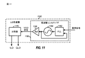
[00110]図11は、LO生成器1100の例示的な一設計を示し、それは本明細書に記載したLO生成器のいずれにも使用され得る。LO生成器1100は、(i)所望の周波数で電圧制御発振器(VCO)信号を生成するための周波数シンセサイザ1160と、(ii)VCO信号を周波数について分周し、ILO信号およびQLO信号を備えるLO信号を提供する、ための分周器1170と、を含む。
[00110] FIG. 11 shows an exemplary design of the
[00111]図11において示した例示的な設計では周波数シンセサイザ1160は、PLL1162と、VCO1164と、バッファ(Buf)1166と、を含む。VCO1164は、PLL1162から制御信号を受け取るとともに制御信号によって決定される周波数の発振器信号を生成する。PLL1162は、VCO1164から基準信号および発振器信号を受け取り、発振器信号の位相を基準信号の位相に対して比較し、発振器信号の位相が基準信号の位相に合わせて固定されるようにVCO1164のための制御信号を生成する。バッファ1166は、VCO1164から発振器信号を受け取り、VCO信号を分周器1170に提供する。分周器1170は周波数についてVCO信号をN分の1に分周する(ここでNは、2、3、4または何らかの他の値と等し得る)。分周器1170は、ILO信号とQLO信号とを提供する。ILO信号とQLO信号の各々を差分LO信号とし得る。
[00111] In the exemplary design shown in FIG. 11, the
[00112]第1の受信機(たとえば、非起動の受信機)のためのLO生成器が、較正される第2の受信機に関するLO信号を生成するために使用され得る。これは様々な方式で達成され得る。例示的な一設計では、直流(DC)電圧が、ミキサに加えられ、第2の受信機に関するテスト信号を生成するためにLO生成器からのLO信号によってアップコンバートされ得る。たとえば図9において、低域通過フィルタ970a内のスイッチ972および976が開放され得、DC電圧がノードN3およびN4に提供され得る。このDC電圧は、ミキサ961aおよび/または961bに関するテスト信号を生成するためにミキサ960aによってILO1信号を用いてアップコンバートされることがある。テスト信号の振幅はDC電圧に依存し得、DC電圧を変動させることによって所望のテスト信号振幅が取得され得る。たとえば、DC電圧を0.2Vから1.0Vまで変動させることによって−12dBm〜−30dBmの範囲のテスト信号が生成され得る。例示的な一設計では、低域通過フィルタ970aの1つの入力をプログラマブル共通モード電圧(VCM)に接続し、低域通過フィルタ970aの他の入力を回路の接地に接続することによってDC電圧が生成され得る。このプログラマブルVCMに基づいて調節可能な差分DC電圧が取得され得る。調節可能なDC電圧はまた、可変振幅のテスト信号の生成を可能とする他の方式で生成され得る。
[00112] An LO generator for a first receiver (eg, a non-activated receiver) may be used to generate an LO signal for the second receiver to be calibrated. This can be accomplished in various ways. In one exemplary design, a direct current (DC) voltage may be applied to the mixer and upconverted with the LO signal from the LO generator to generate a test signal for the second receiver. For example, in FIG. 9, switches 972 and 976 in
[00113]別の例示的な設計では、ミキサは、ミキサと増幅器のいずれとしても動作するように再構成可能であり得る。たとえば図9におけるミキサ960aはさらに、2つの追加的なNMOSトランジスタを含みうる。第1のNMOSトランジスタは、ノードN3に結合されたそのソースと、制御信号を受け取るそのゲートと、VDD給電に結合されたそのドレインと、を有し得る。第2のNMOSトランジスタは、回路接地に結合されたそのソースと、制御信号を受け取るゲートと、ノードN4に結合されたそのドレインと、を有し得る。ミキサ960aは、2つのNMOSトランジスタをOFFに切替えることによってミキサとして構成され得る。ミキサ960aは、2つのNMOSトランジスタをONに切替えかつNMOSトランジスタ964aおよび966aをOFFに切替えることによって増幅器として再構成され得る。この場合には、ILO1信号がこの増幅器によって増幅され得、増幅されたLO信号がノードN3およびN4に提供され得る。増幅されたLO信号は、テスト信号を生成するために使用され得る。
[00113] In another exemplary design, the mixer may be reconfigurable to operate as both a mixer and an amplifier. For example, the
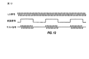
[00114]図12は、LO信号に振幅変調(AM)を適用することによるテスト信号の生成の例示的な一設計を示している。このLO信号は、ある特定の周波数の連続信号であり得る。変調信号m(t)は、パルス列を含み得、振幅変調を有するテスト信号を生成するようにLO信号を振幅変調するために使用され得る。テスト信号は、IIP2および/または他の性能メトリックスを較正するために使用され得る。 [00114] FIG. 12 shows an exemplary design of test signal generation by applying amplitude modulation (AM) to the LO signal. This LO signal may be a continuous signal of a certain frequency. The modulation signal m (t) can include a pulse train and can be used to amplitude modulate the LO signal to produce a test signal having amplitude modulation. The test signal can be used to calibrate IIP2 and / or other performance metrics.
[00115]変調信号m(t)は、LO信号を発生する第1の受信機から較正される第2の受信機への信号経路内の様々な箇所に加えられ得る。たとえば変調信号は、図10Aのカスケードトランジスタ944および/または950のゲートに、図10Bのパストランジスタ952のゲートに、または図10Cのトランジスタ953および955のゲートに加えられ得る。
[00115] The modulated signal m (t) may be applied at various points in the signal path from the first receiver generating the LO signal to the second receiver being calibrated. For example, the modulation signal may be applied to the gate of
[00116](非起動状態にある)第1の受信機のためのLO生成器を用いて(較正される)第2の受信機に関するテスト信号を生成することは、様々な利点を提供し得る。第一にLO生成器は、関心のある周波数範囲に関する、所望の周波数分解能および精度の、LO信号を生成することを可能であり得る。これは、起動状態または非起動状態の間に第2の受信機の較正を可能とし得る。たとえばLO生成器はLO信号を、(i)結果として生じるダウンコンバートされた信号がバンド内較正に関するシステムバンド幅内であるような第1の周波数で、あるいは(ii)結果として生じるダウンコンバートされた信号がバンド外較正に関するシステムバンド幅の外側にあるような第2の周波数で、生成し得る。LO生成器は、周波数においてホップするように、たとえば、TX周波数のホッピングを整合させダウンコンバートされたRX周波数でのIIP2の較正を可能とするTX周波数のホッピングを合わせるように、LO信号を生成し得る。RX周波数は、時分割複信(TDD)に関するTX周波数と同じとすることがあり、あるいは周波数分割複信(FDD)に関するTX周波数と異ならせることがある。 [00116] Generating a test signal for a second receiver (calibrated) using an LO generator for the first receiver (in an unactivated state) may provide various advantages. . First, the LO generator may be able to generate an LO signal with the desired frequency resolution and accuracy for the frequency range of interest. This may allow calibration of the second receiver during the activated state or the unactivated state. For example, the LO generator may convert the LO signal (i) at a first frequency such that the resulting downconverted signal is within the system bandwidth for in-band calibration, or (ii) the resulting downconverted signal. It can be generated at a second frequency such that the signal is outside the system bandwidth for out-of-band calibration. The LO generator generates an LO signal to hop in frequency, for example, to match TX frequency hopping and to align TX frequency hopping that allows IIP2 calibration at the downconverted RX frequency. obtain. The RX frequency may be the same as the TX frequency for time division duplex (TDD) or may be different from the TX frequency for frequency division duplex (FDD).
[00117]これに対して、テスト信号を発生させるための単独のトーン生成器を使用することは、回路の複雑性およびコストを増大させる。さらにトーン生成器は、追加的な回路および制御を含めることなくして要求された周波数範囲および/または要求された精度を有しないことがある。 [00117] In contrast, using a single tone generator to generate a test signal increases the complexity and cost of the circuit. Furthermore, the tone generator may not have the required frequency range and / or the required accuracy without including additional circuitry and control.
[00118]ワイヤレスデバイス110は、厳格な性能仕様を満たすように要求され得、良好なRSBおよび良好なIIP2なくしてこれらの仕様を満たすことができないことがある。たとえばワイヤレスデバイス110は、4×4のMIMO送信について概ね300メガビット/秒(Mbps)のピークスループットを満たすように要求され得、またスループット要件を満たすために45デシベル(dB)またはこれより良好なRSBを要求し得る。RSBは、温度、周波数、その他に対して敏感であり得る。RSBに関する受信機の較正は、製造中に工場で実行され得る。しかしながら、RSBに関する工場の較正によって選択される受信機設定は、温度、周波数、その他にわたる要求されるRSBを提供できないことがある。
[00118] The
[00119]IIP2に関する受信機の較正もまた、1つまたは複数の指定の周波数において工場で実行され得る。しかしながら、ワイヤレスデバイス110は、IIP2較正が実行された周波数のうちの1つにも対応しないTX周波数で送信することがあり得る。この場合には、準最適な(sub-optimal)IIP2のためにいくつかの性能劣化が存在し得る。したがって、ワイヤレスデバイス110のTX周波数に対応するRX周波数でIIP2較正を実行することが望ましくまたは必要であり得る。
[00119] Receiver calibration for IIP2 may also be performed at the factory at one or more specified frequencies. However, the
[00120]本開示の別の態様では、受信機の(たとえば、RSBおよび/またはIIP2に関する)較正は、受信機に関する良好な性能を得るためにワイヤレスデバイス110の動作中に実行され得る。ワイヤレスデバイス110は、与えられた任意の瞬間に接続モードまたは待機モードで動作し得る。接続モードではワイヤレスデバイス110は、1つまたは複数の基地局にデータを送信することおよび/または1つまたは複数の基地局からデータを受信し得る。待機モードではワイヤレスデバイス110は、指定された時間期間中に基地局からダウンリンク信号を周期的に受信し得、また残りの時間中は電池のパワーを節約するためにスリープし得る。
[00120] In another aspect of the present disclosure, calibration of the receiver (eg, for RSB and / or IIP2) may be performed during operation of the
[00121]例示的な一設計ではワイヤレスデバイス110は、ダウンリンク信号を受け取っていない時間期間中に待機モードにおいて較正を実行し得る。別の例示的な設計ではワイヤレスデバイス110は、受信機がダウンリンク受信に使用されていない時間期間の間に接続モードにおいて受信機に関して較正を実行し得る。たとえばTDDを利用するワイヤレスシステムでは、ワイヤレスデバイス110はアップリンクサブフレームにおいてデータを送信し、ダウンリンクサブフレームにおいてデータを受信し得る。ワイヤレスデバイス110は、アップリンクサブフレームの間に受信機を較正し得る。待機モードと接続モードの両方に適用可能なさらに別の例示的な設計では、ワイヤレスデバイス110は、システムバンド幅の外側に配置されたテスト信号を使用することによって、ダウンリンク受信の間に受信機に関する較正を実行し得る。
[00121] In an exemplary design, the
[00122]図13は、第2の受信機1330bによって生成されたテスト信号を用いて第1の受信機1330aを較正するための例示的な一構成を示している。受信機1330bは非起動であり得、受信機1330aに関する所望の周波数のテスト信号を生成するために使用され得る。受信機1330aのLO生成器1380は、fLO1の所望の周波数で第1のLO信号を生成し得る。受信機1330bのLO生成器1382は、fLO2の周波数で第2のLO信号を生成し得る。第2のLO信号は、受信機1330aに関するのテスト信号を生成するために使用され得る。このテスト信号は、受信機1330aに関するLNA1340aの入力(図13には図示せず)に適用され得、受信機1330a内の他のいくつかのノードに加えられ得る。いずれの場合にもテスト信号は、LO生成器1380からのILO1信号を用いてミキサ1360aによってダウンコンバートされ、I入力ベースバンド信号(IBBin)を取得するために低域通過フィルタ1370aによってフィルタ処理され得る。テスト信号はまた、LO生成器1380からのQLO1信号を用いてミキサ1360bによってダウンコンバートされ、Q入力ベースバンド信号(QBBin)を取得するために低域通過フィルタ1370bによってフィルタ処理され得る。ILO1信号とQLO1信号は、受信機1330aのためにLO生成器1380によって生成される第1のLO信号の一部である。IBBin信号とQBBin信号とは、データプロセッサに受信機1330aによって提供される複素BBin信号を形成する。
[00122] FIG. 13 shows an exemplary configuration for calibrating the
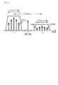
[00123]図14Aは、テスト信号がバンド内に配置されるケースに関する図13における受信機1330aからのBBin信号の周波数応答を示している。具体的には、受信機1330bからの第2のLO信号の周波数fLO2は、受信機1330aにおける第1のLO信号の周波数fLO1からシステムバンド幅(BW)の半分未満だけオフセットされることがある、すなわちf1=|fLO2−fLO1|<BW/2である。これにより、BBin信号が周波数f1の単一トーンを含むことになり、それは図14Aにおいて示したようにシステムバンド幅の域内にある。
[00123] FIG. 14A shows the frequency response of the BBin signal from the
[00124]BBin信号は次のように表現され得る。
![]()
![]()
ここで、I(t)はIBBin信号を意味し、またQ(t)はQBBin信号を意味しており、
BBin(t)は複素BBin信号を意味しており、
kは受信機1330aのIとQとの信号経路の間のゲイン誤差であり、かつ
Θは受信機1330aのIとQとの信号経路の間の位相誤差である。
Here, I (t) means the IBBin signal, and Q (t) means the QBBin signal.
BBin (t) means complex BBin signal,
k is the gain error between the I and Q signal paths of the
[00125]ゲイン誤差kおよび位相誤差Θは次のようにして決定され得る。
![]()
![]()
![]()
![]()
[00126]ゲイン誤差と位相誤差は適当な回路を用いてアナログ領域で決定され得る。別法としてゲイン誤差と位相誤差は、IおよびQのサンプルに対する計算を実行することによってディジタル領域で算出され得、それはIBBin信号とQBBin信号をディジタル化によって取得され得る算出。ゲイン誤差と位相誤差は周波数に依存し得、また関心のある異なる周波数について算出され得る。 [00126] Gain and phase errors can be determined in the analog domain using appropriate circuitry. Alternatively, gain error and phase error can be calculated in the digital domain by performing calculations on the I and Q samples, which can be obtained by digitizing the IBBin and QBBin signals. Gain and phase errors can be frequency dependent and can be calculated for different frequencies of interest.
[00127]図14Bは、テスト信号がバンド外に配置されるケースに関する図13の受信機1330aからのBBin信号の周波数応答を示している。具体的には受信機1330b内の第2のLO信号の周波数fLO2は、受信機1330a内の第1のLO信号の周波数fLO1から、システムバンド幅(BW)の半分を超えるだけオフセットされ得る、すなわちf2=|fLO2−fLO1|>BW/2である。したがってこれにより、周波数f2の単一トーンを含んだBBin信号が得られ、それは図14Bに示したようにシステムバンド幅の域外にある。この構成は、ダウンリンク信号を受信している間に受信機1330aを較正するために使用され得る。
[00127] FIG. 14B shows the frequency response of the BBin signal from the
[00128]図14Cは、較正のためにAM変調されたテスト信号が使用されるケースに関する図13の受信機1330aからのBBin信号の周波数応答を示している。受信機1330b内の第2のLO信号の周波数fLO2は受信機1330a内の第1のLO信号の周波数fLO1から、TX周波数とRX周波数の差であるTXオフセットだけオフセットされ得る。第2のLO信号は、図14Cに示したようにBBin信号がシステムバンド幅内に異なる周波数のダウンコンバートされたトーンを含むように周波数においてホッピングし得る。
[00128] FIG. 14C shows the frequency response of the BBin signal from the
[00129]例示的な一設計では、異なるバンドグループにおける異なる周波数で較正が実行され得る。たとえば較正は、ローバンド内の4つのサブバンド、ミッドバンド内の4つのサブバンド、およびハイバンド内の2つのサブバンドに対して実行され得る。較正はまた、ローバンド内の各サブバンドにある3つの周波数、ミッドバンド内の各サブバンドにある3つの周波数、およびハイバンド内の各サブバンドにある2つの周波数に対して実行され得る。較正はしたがって、この例では(3*4+3*4+4*2)=32の周波数に対して実行され得る。較正はまた、これより少ない周波数または多い周波数に対して実行され得る。 [00129] In an exemplary design, calibration may be performed at different frequencies in different band groups. For example, calibration may be performed for four subbands in the low band, four subbands in the midband, and two subbands in the high band. Calibration may also be performed for three frequencies in each subband in the low band, three frequencies in each subband in the midband, and two frequencies in each subband in the high band. Calibration can therefore be performed for (3 * 4 + 3 * 4 + 4 * 2) = 32 frequencies in this example. Calibration can also be performed for fewer or more frequencies.
[00130]ワイヤレスデバイス110は、受信経路ゲインに関する厳格な仕様を満たすように(たとえば、±1dB以内のゲイン確度を満たすように)要求され得る。受信経路ゲインは受信経路のゲインとして規定され得る。受信経路は、アンテナからアナログ対ディジタル変換器(ADC)までの信号経路の全部または一部をカバーし得る。受信経路は、受信機内の信号経路を、および受信機内のLNAの前のフロントエンドにある信号経路をカバーし得る。ワイヤレスデバイス110は、複数のバンド、複数の無線技術、複数のアンテナ、その他をサポートするために複合的なフロントエンドを有し得る。複合的なフロントエンドであるために受信経路のゲインに対する較正は、受信経路のゲインに関して要求された仕様が満たされ得ることを確実にするためにフロントエンド回路を含むべきである。
[00130] The
[00131]ワイヤレスデバイスは、いくつかの受信経路といくつかのゲインモードを含み得る。受信経路の各ゲインモードはその受信経路に関するある特定のゲインと関連付けされ得る。従来では、受信経路のゲインに対する厳格な仕様は関心のある各ゲインモードおよび各受信経路を較正するようにワイヤレスデバイス内に較正/トーン信号を注入するための外部のテスト装置を用いることによって達成され得る。ワイヤレスデバイスは、多くの数の受信経路および/または多くの数のゲインモードを含み得る。したがって長い時間が、異なる受信経路および異なるゲインモードを較正するために必要とされ、それは複雑性およびコストを増大させ得る。 [00131] A wireless device may include several receive paths and several gain modes. Each gain mode of a receive path can be associated with a specific gain for that receive path. Traditionally, stringent specifications for the gain of the receive path are achieved by using an external test device to inject a calibration / tone signal into the wireless device to calibrate each gain mode of interest and each receive path. obtain. A wireless device may include a large number of receive paths and / or a large number of gain modes. Thus, a long time is required to calibrate different receive paths and different gain modes, which can increase complexity and cost.
[00132]本開示のさらに別の態様では、受信経路のゲインは別の受信機によって生成されたテスト信号に基づいて計測され得る。このテスト信号は、受信経路内の様々な点で注入され得る。受信経路のゲインを決定するために、テスト信号のパワーまたは振幅が計測され得る。 [00132] In yet another aspect of the present disclosure, the gain of the receive path may be measured based on a test signal generated by another receiver. This test signal can be injected at various points in the receive path. To determine the gain of the receive path, the power or amplitude of the test signal can be measured.
[00133]例示的な一設計では、テスト信号を生成し受信経路ゲインを計測するために送信機に対するフィードバック受信機が使用され得る。図8に戻ると、受信機830cを送信機832に対するフィードバック受信機とし得る。フィードバック受信機830cは、方向性結合器822を介してアンテナ810に結合され得る。受信経路ゲイン較正のために追加的なハードウェアがほとんどまたはまったく要求されることがないように、フィードバック受信機830cが受信経路ゲイン較正のために再使用され得る。フィードバック受信機830cは、テスト信号を生成するとともに、このテスト信号をカプラ822に提供することができる。このテスト信号はフロントエンド回路820を通過させられるとともに較正されようとする受信経路に提供され得る。
[00133] In an exemplary design, a feedback receiver for the transmitter may be used to generate the test signal and measure the receive path gain. Returning to FIG. 8, the
[00134]図8に示した例では、様々な信号経路のゲインは次のように規定されることがある。 [00134] In the example shown in FIG. 8, the gain of the various signal paths may be defined as follows.
G1=ノードBからノードCまでのゲイン、
G2=ノードBからノードDまでのゲイン、
L1=ノードXからノードBまでのゲイン、かつ
L2=ノードAからノードBまでのゲイン。
G1 = gain from node B to node C,
G2 = gain from node B to node D,
L1 = gain from node X to node B, and L2 = gain from node A to node B.
G1、G2、L1およびL2はdBの単位で与えられ得る。 G1, G2, L1 and L2 can be given in units of dB.
[00135]テスト信号は、フィードバック受信機830cによって生成され、異なる受信経路の受信経路ゲインを計測するために使用され得る。異なるノードにおけるテスト信号のパワーは次式のように表現され得る。
![]()
![]()
![]()
![]()
![]()
![]()
上式において、PtestはノードXにおけるテスト信号のパワーであり、
P1はノードCにおけるテスト信号のパワーであり、
P2はノードDにおけるテスト信号のパワーであり、かつ
ΔPはノードCおよびDにおける2つの受信経路の間のデルタゲインである。
Where P test is the power of the test signal at node X,
P1 is the power of the test signal at node C;
P2 is the power of the test signal at node D, and ΔP is the delta gain between the two receive paths at nodes C and D.
Ptest、P1およびP2はdBmの単位で与えられ得る。ΔPはdBの単位で与えられ得る。 P test , P1 and P2 can be given in units of dBm. ΔP may be given in units of dB.
[00136]式(6)に示した例示的な設計では、受信機830aが基準として使用される。ノードDにおけるパワーP2は、受信機830aおよび830bに関する2つの受信経路の間のデルタゲインΔPを得るためにノードCにおけるパワーP1から差し引かれ得る。2つの受信経路の間のデルタゲインΔPに関心があるため、デルタゲインが算出されるときに除去されるためにテスト信号の絶対パワーレベルは重要でない。さらにカプラ822の絶対ロスもデルタゲインが算出されるときに除去されるためにこのロスは重要でない。
[00136] In the exemplary design shown in equation (6),
[00137]較正/トーン信号は、外部のテスト装置によって生成されてノードAにあるアンテナコネクタに加えられ得る。ノードCにおける較正信号のパワーは次のように表現され得る。
![]()
![]()
ここで、PinはノードAにおけるテスト装置からの較正信号のパワーであり、および
Pref1はノードCにおける較正信号のパワーである。
Where P in is the power of the calibration signal from the test device at node A, and P ref1 is the power of the calibration signal at node C.
[00138]異なる受信経路のゲインは、ノードAおよびCにおける較正信号のパワーレベルとデルタゲインとに基づいて次のようにして算出され得る。
![]()
![]()
![]()
![]()
上式において、A1はノードAからノードCまでの受信経路のゲインであり、および
A2はノードAからノードDまでの受信経路のゲインである。
In the above equation, A1 is the gain of the reception path from node A to node C, and A2 is the gain of the reception path from node A to node D.
[00139]Pref1を取得するために工場において絶対パワー計測が行われることがある。他のすべての計測は、都合のよい任意の時点で行われ得、それで受信経路ゲイン較正のテスト時間が短縮されることができ、それは全体のテスト時間およびコストを低減し得る。 [00139] may be absolute power measurement is performed at the factory to obtain a P ref1. All other measurements can be made at any convenient point in time, so that the test time for receive path gain calibration can be reduced, which can reduce the overall test time and cost.
[00140]ワイヤレスデバイスの回路は、周波数全体にわたって変動するような応答を有することがある。たとえばカプラ822は、良好な挙動であり得およびそれゆえに事前に特徴付けされ得る周波数応答を有し得る。変圧器またはバラン(図8には図示せず)は、LNA840cをカプラ822とインターフェースさせるために使用され得、および事前に特徴付けされ得るような良好な挙動の周波数応答を有し得る。テスト信号を生成するために使用される回路はまた、事前に特徴付けされ得るような良好な挙動の周波数応答を有し得る。すべての回路の周波数応答に基づいて全体的な周波数応答が取得され得る。参照テーブルは、1つまたは複数の基準周波数の1つまたは複数のゲイン関連する異なる周波数におけるゲインに対応する相対ゲインを保持し得る。
[00140] The circuitry of the wireless device may have a response that varies across frequencies. For example, the
[00141]基準受信経路に関して異なる周波数でいくつかの絶対パワー計測が(たとえば、テスト装置を用いて)行われることがある。基準受信経路に関する他の周波数における絶対パワー計測値は、基準受信経路に関して行われた絶対パワー計測値と、またさらには基準受信経路の事前に特徴付けられた周波数応答と、に基づいて取得され(たとえば、補間され)得る。異なる周波数での他の受信経路に関するおよび異なるゲインモードに関するパワー計測は、(たとえば、フィードバック受信機830cからの)テスト信号に基づいて行われ得る。絶対ゲインは、テスト信号によるパワー計測と、基準信号経路に関して行われた絶対パワー計測とに基づいて、異なる受信経路と異なるゲインモードとに関して決定され得る。内部生成のテスト信号を用いた受信ゲイン較正は、関心のあるすべての受信経路、ゲインモードおよび周波数に関する受信経路のゲインを決定するために必要とされる絶対パワー計測の回数を大幅に低減し得る。
[00141] Several absolute power measurements may be made (eg, using a test device) at different frequencies with respect to the reference receive path. Absolute power measurements at other frequencies for the reference receive path are obtained based on the absolute power measurements made on the reference receive path, and even the pre-characterized frequency response of the reference receive path ( For example, interpolated). Power measurements for other receive paths at different frequencies and for different gain modes may be made based on test signals (eg, from
[00142]一般に受信ゲイン較正は、任意の時点で実行され得る。例示的な一設計では受信ゲイン較正は、受信ゲイン較正だけのために追加的なテスト時間が使われないように、製造の間に、たとえば、他のRFテスト(たとえば、RSB向けなど)と同時に、実行され得る。別の例示的な設計では受信ゲイン較正は、ワイヤレスデバイスの動作中に実行され得る。たとえば受信ゲイン較正は、たとえば受信回路と関連する温度ドリフトのような温度依存の要因を除去するために、ワイヤレスデバイスのスリープ−ウェイクアップのサイクル中に実行され得る。 [00142] In general, receive gain calibration may be performed at any time. In one exemplary design, receive gain calibration is performed during manufacturing, eg, simultaneously with other RF tests (eg, for RSB, etc.) so that no additional test time is used only for receive gain calibration. Can be executed. In another exemplary design, receive gain calibration may be performed during operation of the wireless device. For example, receive gain calibration may be performed during a sleep-wake-up cycle of the wireless device to remove temperature dependent factors such as temperature drift associated with the receive circuit, for example.
[00143]図8は、テスト信号が方向性結合器で提供される、受信経路ゲインを決定するために使用されている例示的な一設計を示している。方向性結合器は、図8に示したようにアンテナの次に配置され得る。一般にテスト信号は、アンテナからADCまでの信号経路内の任意の点で提供され得る。たとえばテスト信号は、ダイプレクサ824とデュプレクサ826または828との間、あるいはLNA840aまたは840bの入力、その他の位置に提供され得る。テスト信号は、方向性結合器、またはスイッチ(たとえば、単極双投(SPDT)スイッチ)、または他のいくつかの回路を介して加えられ得る。ゲインは、テスト信号を通すために経由するすべての回路について計測され得る。
[00143] FIG. 8 shows an exemplary design used to determine the receive path gain, where a test signal is provided at the directional coupler. The directional coupler can be placed next to the antenna as shown in FIG. In general, the test signal can be provided at any point in the signal path from the antenna to the ADC. For example, a test signal may be provided between
[00144]図8は、フロントエンド回路の例示的な一設計を示している。一般にフロントエンド回路は、デュプレクサ、ダイプレクサ、スイッチ、フィルタ、カプラ、その他などの様々な回路を含むことがある。フロントエンド回路内の回路は図8に示した例示的な構成と異なるように構成され得る。 [00144] FIG. 8 shows an exemplary design of a front-end circuit. In general, a front-end circuit may include various circuits such as a duplexer, a diplexer, a switch, a filter, a coupler, and the like. The circuitry within the front end circuit may be configured differently than the exemplary configuration shown in FIG.
[00145]図8は、フィードバック受信機830cに基づいた受信ゲイン較正に関するテスト信号の生成に関する例示的な一設計を示している。一般に受信ゲイン較正のためのテスト信号は任意の回路によって生成され得る。たとえばテスト信号は、テスト中でない受信機、送信機、テスト信号を生成するように設計されたテスト信号生成器、その他によって生成され得る。テスト信号は、ミキサを介してまたは他のいくつかの技法に基づいてDC電圧をアップコンバートすることによって生成され得る。
[00145] FIG. 8 shows an exemplary design for generating a test signal for receive gain calibration based on the
[00146]例示的な一設計では、装置(たとえば、ワイヤレスデバイス、IC、回路モジュール、その他)は第1および第2のLO生成器を含むことがある。第1のLO生成器(たとえば、図5〜図6CのLO生成器580)は、周波数ダウンコンバートのために第1の受信機(たとえば、受信機530)によって使用される第1のLO信号を生成し得る。第2のLO生成器(たとえば、LO生成器582)は、第1の動作モード(たとえば、RXモード)における周波数ダウンコンバートのために第2の受信機(たとえば、受信機532)によって使用される第2のLO信号を生成し得る。第2のLO信号は、第2の動作モード(たとえば、較正モード)において第1の受信機に関するテスト信号を生成するために使用され得る。第1のLO信号はまた、第2の動作モードにおいて第2の受信機に関する第2のテスト信号を生成するために使用され得る。第1の受信機に関するテスト信号は第2の動作モードの第1の構成において生成されることがあり、第2の受信機に関する第2のテスト信号は第2の動作モードの第2の構成において生成され得る。
[00146] In an exemplary design, an apparatus (eg, a wireless device, IC, circuit module, etc.) may include first and second LO generators. A first LO generator (eg,
[00147]例示的な一設計では第1の受信機(たとえば、図7Bの受信機732a)は、第1の組の少なくとも1つのキャリアに関して周波数ダウンコンバートを実行することがあり、第2の受信機(たとえば、図7Bの受信機732b)はたとえば図7Bおよび図7Cに示したようにキャリアアグリゲーションのための第2の組の少なくとも1つのキャリアに関して周波数ダウンコンバートを実行し得る。別の例示的な設計では、第2の受信機(たとえば、図8の受信機830c)を送信機のためのフィードバック受信機とし得、また第2のLO信号がフロントエンド回路を介して第1の受信機(たとえば、図8の受信機830a)に提供され得る。一般に第1および第2の受信機は、ワイヤレスデバイス内の任意の2つの受信機とし得、また同じICチップ上に存在させることも異なるICチップ上に存在させ得る。
[00147] In an exemplary design, a first receiver (eg,
[00148]例示的な一設計ではスイッチは、テスト信号を1つの受信機から別の受信機に渡すために使用され得る。例示的な一設計ではスイッチは第2のLO信号をテスト信号として渡すために単に閉じられるだけのことがある。別の例示的な設計ではスイッチは、変調信号および第2のLO信号を受け取るとともに、この変調信号に基づいて振幅変調を有するテスト信号を提供し得る。 [00148] In one exemplary design, a switch may be used to pass test signals from one receiver to another. In one exemplary design, the switch may simply be closed to pass the second LO signal as a test signal. In another exemplary design, the switch may receive the modulation signal and the second LO signal and provide a test signal having amplitude modulation based on the modulation signal.
[00149]例示的な一設計では装置はさらに、第1および第2のLNAとスイッチとを含み得る。第1のLNA(たとえば、図7AのLNA740または図10A〜図10CのLNA940)は、第1の入力RF信号を受け取り、第1の増幅されたRF信号を第1の受信機に提供し得る。第2のLNA(たとえば、図7AのLNA741または図10A〜図10CのLNA942)は、第2の入力RF信号を受け取り、第2の増幅されたRF信号を第2の受信機に提供し得る。スイッチは、第1のLNAと第2のLNAの間に結合され得、また第2の動作モードにおいてテスト信号を渡し得る。
[00149] In one exemplary design, the apparatus may further include first and second LNAs and switches. A first LNA (eg,
[00150]例示的な一設計ではスイッチは、第1の受信機の第1のLNAと第2の受信機の第2のLNAの間に結合されたトランジスタ(たとえば、図7Aのトランジスタ758、図10Aのトランジスタ950、または図10Bのトランジスタ952)を備え得る。別の例示的な設計ではスイッチは3つのトランジスタを備え得る。第1のトランジスタ(たとえば、図10Cのトランジスタ953)は第1のLNAと中間ノードの間に結合され得る。第2のトランジスタ(たとえば、トランジスタ955)は、中間ノードと第2のLNAの間に結合され得る。第3のトランジスタ(たとえば、トランジスタ957)は、中間ノードと回路接地の間に結合され得る。
[00150] In an exemplary design, the switch is a transistor coupled between a first LNA of a first receiver and a second LNA of a second receiver (eg,
[00151]別の例示的な設計では装置はさらに、ゲイン回路と第1および第2のカスケードトランジスタとを備えたSIMO LNA(たとえば、図7BのSIMO LNA742)を含むことがある。ゲイン回路(たとえば、ゲイン回路752a)は入力RF信号を受け取りかつ増幅させ得る。第1のカスケードトランジスタ(たとえば、カスケードトランジスタ754a)は、ゲイン回路に結合されることがあり、また第1の増幅されたRF信号を第1の受信機に提供し得る。第2のカスケードトランジスタ(たとえば、カスケードトランジスタ754b)は、ゲイン回路に結合され得、また第2の増幅されたRF信号を第2の受信機に提供し得る。第1および第2のカスケードトランジスタは、たとえば図7Bに示したように第2の動作モードにおいてテスト信号を第1の受信機に渡すためにONに切替えられ得る。
[00151] In another exemplary design, the apparatus may further include a SIMO LNA (eg,
[00152]さらに別の例示的な設計では装置はさらに、SIMO LNAに関して上述したゲイン回路と第1および第2のカスケードトランジスタと、またさらには第2のゲイン回路と第3および第4のカスケードトランジスタとを備えたMIMO LNA(たとえば、図7CのMIMO LNA744)を含み得る。第2のゲイン回路(たとえば、図7Cのゲイン回路752b)は第2の入力RF信号を受け取りかつ増幅させ得る。第3のカスケードトランジスタ(たとえば、カスケードトランジスタ754c)は、第2のゲイン回路に結合され得、また第3の増幅されたRF信号を第1の受信機に提供し得る。第4のカスケードトランジスタ(たとえば、カスケードトランジスタ754d)は、第2のゲイン回路に結合され得、また第4の増幅されたRF信号を第2の受信機に提供し得る。
[00152] In yet another exemplary design, the apparatus further includes a gain circuit and first and second cascade transistors as described above with respect to the SIMO LNA, and even a second gain circuit and third and fourth cascade transistors. And a MIMO LNA (eg,
[00153]例示的な一設計では第2の受信機は、ミキサ(たとえば、図13のミキサ1360c)を備得うる。このミキサは、第1の動作モードにおいて第2のLO信号によって入力RF信号をダウンコンバートし得る。このミキサは、中間LO信号を取得するために第2の動作モードにおいて第2のLO信号によってDC電圧を逓昇変換し得、それはテスト信号の生成のために使用され得る。このDC電圧は、テスト信号に関する調節可能な振幅を得るために変動させることがある。
[00153] In one exemplary design, the second receiver may comprise a mixer (eg,
[00154]第1のLO生成器は第1の周波数で第1のLO信号を生成することがあり、かつ第2のLO生成器は第2の周波数で第2のLO信号を生成し得る。例示的な一設計では第2の周波数は、たとえば図14Aに示したように第1の周波数から、システムバンド幅の半分未満とし得る。別の例示的な設計では第2の周波数は、たとえば図14Bに示したように第1の周波数から、システムバンド幅の半分を超えるようにし得る。この例示的設計では、信号の受信および較正が同時に実行され得、また第1および第2の動作モードが同時に選択され得る。さらに別の例示的な設計では第2のLO生成器は、たとえば図14Cに示したように複数の周波数のテスト信号を得るために、第2のLO信号を複数の周波数で(たとえば、周波数ホッピングを用いて)生成し得る。 [00154] The first LO generator may generate a first LO signal at a first frequency, and the second LO generator may generate a second LO signal at a second frequency. In one exemplary design, the second frequency may be less than half of the system bandwidth, eg, from the first frequency as shown in FIG. 14A. In another exemplary design, the second frequency may be greater than half of the system bandwidth from the first frequency, eg, as shown in FIG. 14B. In this exemplary design, signal reception and calibration can be performed simultaneously, and the first and second operating modes can be selected simultaneously. In yet another exemplary design, the second LO generator may generate the second LO signal at multiple frequencies (eg, frequency hopping, for example, to obtain a multiple frequency test signal as shown in FIG. 14C. Can be generated).
[00155]第2のLO信号は、第2の受信機が非起動状態にあるときにテスト信号を生成するために使用され得る。例示的な一設計では第2のLO信号は、装置が待機モードで動作している時点での第1の受信機の較正のためのテスト信号を生成するために使用され得る。第2の受信機は、待機モードにおける信号の受信のために、ある時間期間の間だけ周期的に起動状態となることがある。較正は、第2の受信機が起動状態でない残りの時間中に実行され得る。別の例示的な設計では第2のLO信号は、装置が接続モードで動作している時点での第1の受信機の較正のためのテスト信号を生成するために使用され得る。たとえばテスト信号は、信号バンド幅の外側(たとえば、図14Bに示したようなバンド幅)で生成され得、それは信号受信と同時に較正が実行され得る。別法としてTDDの場合は、装置がアップリンクで送信しているアップリンク時間間隔の間で第2の受信機の較正が実行され得る。 [00155] The second LO signal may be used to generate a test signal when the second receiver is in a non-activated state. In one exemplary design, the second LO signal may be used to generate a test signal for calibration of the first receiver when the device is operating in standby mode. The second receiver may be periodically activated for a certain period of time for reception of signals in standby mode. The calibration can be performed during the remaining time that the second receiver is not active. In another exemplary design, the second LO signal may be used to generate a test signal for calibration of the first receiver when the device is operating in connected mode. For example, the test signal can be generated outside the signal bandwidth (eg, the bandwidth as shown in FIG. 14B), which can be calibrated simultaneously with signal reception. Alternatively, in the case of TDD, calibration of the second receiver may be performed during the uplink time interval that the device is transmitting on the uplink.
[00156]図15は、較正を実行するためのプロセス1500の例示的な一設計を示している。第1のLO信号は、第1のLO生成器によって生成され得、また周波数ダウンコンバートのために第1の受信機によって使用され得る(ブロック1512)。第2のLO信号は第2のLO生成器よって生成され得、また第1の動作モードにおいて周波数ダウンコンバートのために第2の受信機によって使用され得る(ブロック1514)。第1の受信機に関するテスト信号は、第2の動作モードにおいて第2のLO信号に基づいて生成され得る(ブロック1516)。テスト信号は、変調をまったく伴わない第2のLO信号を備え得、あるいは第2のLO信号を変調信号によって振幅変調することによって生成され得る。
[00156] FIG. 15 shows an exemplary design of a
[00157]別の例示的な設計では装置(たとえば、ワイヤレスデバイス、IC、回路モジュール、その他)は、LO生成器、フロントエンド回路および受信機を含み得る。LO生成器(たとえば、図8のLO生成器882)は、テスト信号を取得するために使用されるLO信号を生成し得る。フロントエンド回路(たとえば、フロントエンド回路820)は、テスト信号と受信されたRF信号とを受け取り、入力RF信号を提供し得、それは受信されたRF信号に基づいて生成され得、テスト信号を備え得る。受信機(たとえば、受信機830a)は、フロントエンド回路に結合され得、入力RF信号を受け取り得る。受信経路は、フロントエンド回路に基づいて形成され得、また受信機はテスト信号に基づいて決定されたゲインを有し得る。LO信号は、第1の動作モードにおける周波数ダウンコンバートのために別の受信機(たとえば、受信機830c)によって使用されることがあり、また第2の動作モードにおけるテスト信号の生成のために使用され得る。
[00157] In another exemplary design, an apparatus (eg, wireless device, IC, circuit module, etc.) may include an LO generator, a front-end circuit, and a receiver. An LO generator (eg,
[00158]例示的な一設計ではフロントエンド回路は、方向性結合器(たとえば、図8の方向性結合器822)を含むことがある。方向性結合器は、受信されたRF信号を受け取る第1のポートと、テスト信号を受け取る第2のポートと、結合されたRF信号を提供する第3のポートと、を有し得る。入力RF信号は、この結合されたRF信号に基づいて生成され得る。フロントエンド回路はまた、ダイプレクサ、デュプレクサ、スイッチ、フィルタ、整合回路、その他などの他の回路を含み得る。
[00158] In one exemplary design, the front-end circuit may include a directional coupler (eg, the
[00159]この装置はさらに、第2の受信機(たとえば、受信機830b)を含み得る。第2の受信機は、フロントエンド回路に結合され得第2の入力RF信号を受け取り得、それは受信されたRF信号に基づいて生成され得、テスト信号を備え得る。第2の受信経路は、フロントエンド回路および第2の受信機に基づいて形成され得、テスト信号に基づいて決定された第2のゲインを有し得る。 [00159] The apparatus may further include a second receiver (eg, receiver 830b). The second receiver may be coupled to the front end circuit and may receive a second input RF signal, which may be generated based on the received RF signal and may comprise a test signal. The second receive path may be formed based on the front end circuit and the second receiver and may have a second gain determined based on the test signal.
[00160]図16は、受信経路ゲインを決定するためのプロセス1600の例示的な一設計を示している。テスト信号は、ワイヤレスデバイス上のLO生成器からのLO信号に基づいて生成され得る(ブロック1612)。LO生成器は、受信機および/または送信機による周波数変換のためのLO信号を生成し得る。LO生成器はまた、ワイヤレスデバイスの較正のためだけに使用され得る。ワイヤレスデバイス内の少なくとも1つの受信経路の少なくとも1つのゲインはテスト信号に基づいて決定され得る(ブロック1614)。
[00160] FIG. 16 shows an exemplary design of a
[00161]例示的な一設計ではテスト信号は、ワイヤレスデバイスのフロントエンド回路に加えられ得る。少なくとも1つの受信経路のごとに、フロントエンド回路の少なくとも一部を備得うる。各受信経路はさらに、LNAと、たとえば、図8に示したように、受信機の全部または一部と、を備得うる。 [00161] In an exemplary design, test signals may be applied to the front-end circuitry of the wireless device. For each at least one reception path, at least a portion of the front end circuit may be provided. Each receive path may further comprise an LNA and, for example, all or part of the receiver as shown in FIG.
[00162]図17は、少なくとも1つの受信経路の少なくとも1つのゲインを決定するためのプロセス1614xの例示的な一設計を示している。プロセス1614xは、図16のブロック1614について使用され得る。ゲインは、少なくとも1つの受信経路に関して決定され得、第1の受信経路と第2の受信経路とを備え得る。第1の受信経路を介するテスト信号のパワーが、第1のパワー計測値を取得するために計測され得る(ブロック1712)。第2の受信経路を介するテスト信号のパワーが、第2のパワー計測値を取得するために計測され得る(ブロック1714)。第1の受信経路と第2の受信経路の間のデルタゲインは、たとえば式(6)に示したようにして第1および第2のパワー計測値に基づいて決定され得る(ブロック1716)。第1の受信経路の第1のゲイン(たとえば、絶対ゲイン)は、ワイヤレスデバイスの外部で生成され、ワイヤレスデバイスに加えられる信号に基づいて決定され得る(ブロック1718)。第2の受信経路の第2のゲインは、たとえば式(9)に示したようにして第1のゲインおよびデルタゲインに基づいて決定され得る(ブロック1720)。
[00162] FIG. 17 shows an exemplary design of a
[00163]例示的な一設計では第1の受信経路の第1のゲインは、複数の周波数においてワイヤレスデバイスの外部で生成された信号に基づいて決定され得る。第1の受信経路と第2の受信経路の間のデルタゲインはまた、複数の周波数においてテスト信号に基づいて決定され得る。複数の周波数における第2の受信経路の第2のゲインは、複数の周波数における第1の受信経路の第1のゲインとデルタゲインとに基づいて決定され得る。 [00163] In an exemplary design, the first gain of the first receive path may be determined based on signals generated external to the wireless device at multiple frequencies. The delta gain between the first receive path and the second receive path may also be determined based on the test signal at multiple frequencies. The second gain of the second reception path at the plurality of frequencies may be determined based on the first gain and delta gain of the first reception path at the plurality of frequencies.
[00164]例示的な一設計では、周波数にわたる受信経路のゲインにおける変動を表した情報が、事前に特徴付けられ、たとえば参照テーブル内に、保持され得る。少なくとも1つの周波数における受信経路のゲインは、ワイヤレスデバイスの外部で生成された信号に基づいて決定され得る。この少なくとも1つの周波数における受信経路のゲインと保持されている情報とに基づいて、1つまたは複数の追加的な周波数における受信経路のゲインが決定され得る。 [00164] In an exemplary design, information representing the variation in gain of the receive path over frequency may be pre-characterized and maintained, for example, in a look-up table. The gain of the receive path at the at least one frequency may be determined based on a signal generated outside the wireless device. Based on the received path gain at the at least one frequency and the retained information, the received path gain at one or more additional frequencies may be determined.
[00165]本明細書に記載した回路(たとえば、LO生成器、LNA、ミキサ、フィルタ、スイッチ、その他)は、IC、アナログIC、RFIC、混合信号IC、ASIC、プリント回路基板(PCB)、電子デバイス、その他の上に実装され得る。これらの回路はまた、相補型金属酸化物半導体(CMOS)、NチャンネルMOS(NMOS)、PチャンネルMOS(PMOS)、バイポーラ接合トランジスタ(BJT)、バイポーラCMOS(BiCMOS)、シリコンゲルマニウム(SiGe)、ガリウムヒ素(GaAs)、ヘテロ接合バイポーラトランジスタ(HBT)、高電子移動度トランジスタ(HEMT)、シリコンオンインシュレータ(SOI)、その他などの様々なICプロセス技術によって製作され得る。 [00165] The circuits described herein (eg, LO generators, LNAs, mixers, filters, switches, etc.) are ICs, analog ICs, RFICs, mixed signal ICs, ASICs, printed circuit boards (PCBs), electronic Can be implemented on devices, etc. These circuits also include complementary metal oxide semiconductors (CMOS), N-channel MOS (NMOS), P-channel MOS (PMOS), bipolar junction transistors (BJT), bipolar CMOS (BiCMOS), silicon germanium (SiGe), gallium. It can be fabricated by various IC process technologies such as arsenic (GaAs), heterojunction bipolar transistor (HBT), high electron mobility transistor (HEMT), silicon on insulator (SOI), etc.
[00166]本明細書に記載した回路を実装する装置は、スタンドアロンデバイスとし得、またはより大型のデバイスの一部とし得る。デバイスは、(i)スタンドアロンIC、(ii)データおよび/または命令を保存するためのメモリICを含み得る1つまたは複数のICの組、(iii)RF受信機(RFR)やRF送信機/受信機(RTR)などのRFIC、(iv)移動局モデム(MSM)などのASIC、(v)他のデバイス内に埋め込まれ得るモジュール、(vi)受信機、携帯電話、ワイヤレスデバイス、ハンドセットやモバイルユニット、(vii)その他、とし得る。 [00166] An apparatus for implementing the circuits described herein may be a stand-alone device or may be part of a larger device. The device may include (i) a stand-alone IC, (ii) a set of one or more ICs that may include a memory IC for storing data and / or instructions, (iii) an RF receiver (RFR), an RF transmitter / RFICs such as receivers (RTR), (iv) ASICs such as mobile station modems (MSM), (v) modules that can be embedded in other devices, (vi) receivers, mobile phones, wireless devices, handsets and mobiles Unit, (vii) Other, etc.
[00167]1つまたは複数の例示的な設計では記載した機能が、ハードウェアの形、ソフトウェアの形、ファームウェアの形、またはこれらを組合せた形で実装され得る。ソフトウェアの形で実装される場合にこれらの機能は、コンピュータ読み取り可能媒体上の1つまたは複数の命令やコードとして保存されること、あるいはコンピュータ読み取り可能媒体を介して送信され得る。コンピュータ読み取り可能媒体は、コンピュータ記憶媒体とコンピュータプログラムのある箇所から別の箇所への転送を容易にする任意の媒体を含む通信媒体との両方を含む。記憶媒体は、コンピュータによってアクセスでき得る利用可能な任意の媒体とし得る。限定ではなく一例として、このようなコンピュータ読み取り可能媒体はRAM、ROM、EEPROM(登録商標)、CD−ROMや他の光ディスク記憶装置、磁気ディスク記憶装置や他の磁気記憶デバイス、または命令やデータ構造の形態で所望のプログラムコードを持ち運びまたは保存するために使用し得るとともに、コンピュータによってアクセスし得るような他の任意の媒体を備えることが可能である。さらに、任意の接続もコンピュータ読み取り可能媒体と適正に呼ばれる。たとえばウェブサイト、サーバまたは他のリモートのソースからソフトウェアが同軸ケーブル、光ファイバケーブル、ツイストペア、ディジタル加入者線(DSL)、または赤外線、無線およびマイクロ波などのワイヤレス技術を用いて送信される場合、これら同軸ケーブル、光ファイバケーブル、ツイストペア、DSL、または赤外線、無線およびマイクロ波などのワイヤレス技術は媒体の定義の中に含まれる。本明細書で使用する場合にディスク(disk)とディスク(disc)は、コンパクトディスク(CD)、レーザーディスク(登録商標)、光ディスク、ディジタル多目的ディスク(DVD)、フロッピー(登録商標)ディスクおよびブルーレイ(登録商標)ディスクを含む(ただし、ディスク(disk)は通常データを磁気的に再生成する一方、ディスク(disc)はレーザーによってデータを光学的に再生成する)。上記のものの組合せもまた、コンピュータ読み取り可能媒体の趣旨域内に含まれるべきである。 [00167] The functions described in one or more exemplary designs may be implemented in hardware, software, firmware, or a combination thereof. If implemented in software, the functions may be stored as one or more instructions or code on a computer-readable medium, or transmitted via a computer-readable medium. Computer-readable media includes both computer storage media and communication media including any medium that facilitates transfer of a computer program from one place to another. A storage media may be any available media that can be accessed by a computer. By way of example, and not limitation, such computer-readable media can be RAM, ROM, EEPROM®, CD-ROM or other optical disk storage device, magnetic disk storage device or other magnetic storage device, or instruction or data structure. Any other medium that can be used to carry or store the desired program code in the form of and that can be accessed by a computer can be provided. In addition, any connection is properly termed a computer-readable medium. For example, if the software is transmitted from a website, server or other remote source using coaxial cable, fiber optic cable, twisted pair, digital subscriber line (DSL), or wireless technologies such as infrared, radio and microwave, These coaxial cables, fiber optic cables, twisted pair, DSL, or wireless technologies such as infrared, radio and microwave are included in the definition of media. As used herein, a disc and a disc are a compact disc (CD), a laser disc (registered trademark), an optical disc, a digital multipurpose disc (DVD), a floppy (registered trademark) disc, and a Blu-ray ( Registered disk (however, a disk normally regenerates data magnetically, while a disk optically regenerates data with a laser). Combinations of the above should also be included within the spirit of computer-readable media.
[00168]本開示に関する上の記述は当業者による本開示の実施または使用を可能にするために提供されている。当業者には本開示に対する様々な修正が容易に明らかとなろう、また本明細書に規定した一般的な原理に対して本開示の趣旨域を逸脱することなく他の変形形態に適用され得る。したがって本開示は、本明細書に記載した例および設計に限定されるものではなく、本明細書に開示した原理および新規の特徴と矛盾しない最も広い趣旨域が付与されるべきである。
以下に、本願出願の当初の特許請求の範囲に記載された発明を付記する。
[C1]
周波数ダウンコンバートのために第1の受信機によって使用される第1のLO信号を生成するように構成可能な第1の局部発振器(LO)生成器と、
第1の動作モードにおいて周波数ダウンコンバートのために第2の受信機によって使用されおよび第2の動作モードにおいて前記第1の受信機に関するテスト信号を生成するために使用される第2のLO信号を生成するように構成可能な第2のLO生成器と、を備える装置。
[C2]
前記第2のLO生成器は、前記第2の動作モードの第1の構成において前記第1の受信機に関する前記テスト信号を生成するために使用される前記第2のLO信号を生成するように構成可能であり、および前記第1のLO生成器は、前記第2の動作モードの第2の構成において前記第2の受信機に関する第2のテスト信号を生成するために使用される前記第1のLO信号を生成するように構成可能である、C1に記載の装置。
[C3]
前記第1の受信機は、少なくとも1つのキャリアの第1の組に関する周波数ダウンコンバートを実行するように構成可能であり、および前記第2の受信機は、少なくとも1つのキャリアの第2の組に関する周波数ダウンコンバートを実行するように構成可能である、C1に記載の装置。
[C4]
前記第2の受信機は送信機に関するフィードバック受信機であり、および前記第2のLO信号は前記第1の受信機にフロントエンド回路を介して提供される、C1に記載の装置。
[C5]
変調信号と前記第2のLO信号とを受け取るように、および前記変調信号に基づいて振幅変調を有する前記テスト信号を提供するように、構成可能なスイッチをさらに備える、C1に記載の装置。
[C6]
第1の入力無線周波数(RF)信号を受け取りおよび前記第1の受信機に第1の増幅されたRF信号を提供するように、構成可能な第1の低雑音増幅器(LNA)と、
第2の入力RF信号を受け取りおよび前記第2の受信機に第2の増幅されたRF信号を提供するように、構成可能な第2のLNAと、
前記第1のLNAと前記第2のLNAの間に結合され、および前記第2の動作モードにおいて前記テスト信号を渡すように構成可能なスイッチと、をさらに備える、C1に記載の装置。
[C7]
前記スイッチは、前記第1のLNAと前記第2のLNAの間に結合されたトランジスタを備える、C6に記載の装置。
[C8]
前記スイッチは、
前記第1のLNAと中間ノードの間に結合された第1のトランジスタと、
前記中間ノードと前記第2のLNAの間に結合された第2のトランジスタと、
前記中間ノードと回路の接地の間に結合された第3のトランジスタと、を備える、C6に記載の装置。
[C9]
低雑音増幅器(LNA)であって、
入力無線周波数(RF)信号を受け取りおよび増幅するように構成可能なゲイン回路と、
前記ゲイン回路に結合され、および前記第1の受信機に第1の増幅されたRF信号を提供するように構成可能な第1のカスケードトランジスタと、
前記ゲイン回路に結合され、および前記第2の受信機に第2の増幅されたRF信号を提供するように構成可能な第2のカスケードトランジスタ、前記第1および第2のカスケードトランジスタは前記第2の動作モードにおいて前記第1の受信機に前記テスト信号を渡すようにONに切替えられる、と、
を備えた低雑音増幅器、をさらに備える、C1に記載の装置。
[C10]
前記LNAは、
第2の入力RF信号を受け取りおよび増幅するように構成可能な第2のゲイン回路と、
前記第2のゲイン回路に結合されおよび前記第1の受信機に第3の増幅されたRF信号を提供するように構成可能な第3のカスケードトランジスタと、
前記第2のゲイン回路に結合されおよび前記第2の受信機に第4の増幅されたRF信号を提供するように構成可能な第4のカスケードトランジスタと、をさらに備える、C9に記載の装置。
[C11]
前記第2の受信機は、前記テスト信号を生成するために使用される中間LO信号を取得するために、前記第1の動作モードにおいて前記第2のLO信号によって入力無線周波数(RF)信号をダウンコンバートするようにおよび前記第2の動作モードにおいて前記第2のLO信号によって直流(DC)電圧をアップコンバートするように構成可能なミキサを備える、C1に記載の装置。
[C12]
前記第1のLO生成器は、第1の周波数で前記第1のLO信号を生成するように構成可能であり、および前記第2のLO生成器は前記第1の周波数からシステムバンド幅の半分未満の第2の周波数で前記第2のLO信号を生成するように構成可能である、C1に記載の装置。
[C13]
前記第1のLO生成器は、第1の周波数で前記第1のLO信号を生成するように構成可能であり、および前記第2のLO生成器は、前記第1の周波数からシステムバンド幅の半分を超える第2の周波数で前記第2のLO信号を生成するように構成可能である、C1に記載の装置。
[C14]
前記第2のLO生成器は、前記テスト信号を複数の周波数において取得するために前記第2のLO信号を前記複数の周波数で生成するように構成可能である、C1に記載の装置。
[C15]
周波数ダウンコンバートのために第1の受信機によって使用するために第1のLO生成器によって第1の局部発振器(LO)信号を生成することと、
第1の動作モードにおける周波数ダウンコンバートのために第2の受信機によって使用するために第2のLO生成器によって第2のLO信号を生成することと、
第2の動作モードにおいて前記第2のLO信号に基づいて前記第1の受信機に関するテスト信号を生成することと、を備える方法。
[C16]
前記テスト信号を生成することは、変調信号によって前記第2のLO信号を振幅変調することによって前記テスト信号を生成することを備える、C15に記載の方法。
[C17]
前記テスト信号を生成することは、ワイヤレスデバイスの待機モードの間に前記テスト信号を生成することを備える、C15に記載の方法。
[C18]
周波数ダウンコンバートのために第1の受信機によって使用するために第1の局部発振器(LO)信号を生成するための手段と、
第1の動作モードにおける周波数ダウンコンバートのために第2の受信機によって使用するために第2のLO信号を生成するための手段と、
第2の動作モードにおいて前記第2のLO信号に基づいて前記第1の受信機に関するテスト信号を生成するための手段と、を備える装置。
[C19]
前記テスト信号を生成するための前記手段は、変調信号で前記第2のLO信号を振幅変調することによって前記テスト信号を生成するための手段を備える、C18に記載の装置。
[C20]
テスト信号を取得するために使用されるLO信号を生成するように構成可能な局部発振器(LO)生成器と、
前記テスト信号と受信された無線周波数(RF)信号とを受け取るようにおよび前記受信されたRF信号に基づいて生成されならびに前記テスト信号を備えた入力RF信号を提供するように構成可能なフロントエンド回路と、
前記フロントエンド回路に結合されおよび前記入力RF信号を受信するように構成可能な受信機、受信経路は前記テスト信号に基づいて決定されるゲインを有する前記受信機および前記フロントエンド回路に基づいて形成される、と、を備える装置。
[C21]
前記フロントエンド回路は、前記受信されたRF信号を受け取る第1のポートと、前記テスト信号を受け取る第2のポートと、結合されたRF信号を提供する第3のポートと、を有する方向性結合器、前記入力RF信号は前記結合されたRF信号に基づいて生成される、を備えるC20に記載の装置。
[C22]
前記フロントエンド回路に結合され、および前記受信されたRF信号に基づいて生成されならびに前記テスト信号を備えた第2の入力RF信号を受け取るように構成可能な第2の受信機、第2の受信経路は前記テスト信号に基づいて決定された第2のゲインを有する前記第2の受信機および前記フロントエンド回路に基づいて形成される、をさらに備えるC20に記載の装置。
[C23]
ワイヤレスデバイス上でLO生成器からの局部発振器(LO)信号に基づいてテスト信号を生成することと、
前記テスト信号に基づいて前記ワイヤレスデバイスにおける少なくとも1つの受信経路の少なくとも1つのゲインを決定することと、を備える方法。
[C24]
前記テスト信号を前記ワイヤレスデバイスのフロントエンド回路に加えること、前記少なくとも1つの受信経路の各々は前記フロントエンド回路の少なくとも一部を備える、をさらに備える、C23に記載の方法。
[C25]
前記少なくとも1つの受信経路は第1の受信経路と第2の受信経路とを備え、前記少なくとも1つのゲインを決定することは、
第1のパワー計測値を取得するために前記第1の受信経路を介する前記テスト信号のパワーを計測することと、
第2のパワー計測値を取得するために前記第2の受信経路を介する前記テスト信号のパワーを計測することと、
前記第1および第2のパワー計測値に基づいて前記第1と前記第2の受信経路の間のデルタゲインを決定することと、を備える、C23に記載の方法。
[C26]
前記少なくとも1つのゲインを決定することは、
前記ワイヤレスデバイスの外部で生成されるとともに前記ワイヤレスデバイスに加えられる信号に基づいて前記第1の受信経路の第1のゲインを決定することと、
前記第1のゲインおよび前記デルタゲインに基づいて前記第2の受信経路の第2のゲインを決定することと、をさらに備える、C25に記載の方法。
[C27]
前記ワイヤレスデバイスの外部で生成された信号に基づいて複数の周波数において前記第1の受信経路の第1のゲインを決定することと、
前記テスト信号に基づいて前記複数の周波数において前記第1と第2の受信経路の間のデルタゲインを決定することと、
前記複数の周波数における前記デルタゲインおよび前記第1の受信経路の前記第1のゲインに基づいて前記複数の周波数において前記第2の受信経路の第2のゲインを決定することと、をさらに備える、C23に記載の方法。
[C28]
周波数にわたる受信経路のゲインの変動を表した情報を保持することと、前記受信経路は前記少なくとも1つの受信経路のうちの1つである、
前記ワイヤレスデバイスの外部で生成されおよび前記ワイヤレスデバイスに加えられる信号に基づいて少なくとも1つの周波数において前記受信経路の前記ゲインを決定することと、
前記少なくとも1つの周波数における前記受信経路の前記ゲインおよび前記保持された情報に基づいて1つまたは複数の追加的な周波数において前記受信経路の前記ゲインを決定することと、をさらに備える、C23に記載の方法。
[00168] The above description of the disclosure is provided to enable any person skilled in the art to make or use the disclosure. Various modifications to the present disclosure will be readily apparent to those skilled in the art and may be applied to other variations to the general principles defined herein without departing from the scope of the present disclosure. . Accordingly, the present disclosure is not limited to the examples and designs described herein, but is to be accorded the widest scope consistent with the principles and novel features disclosed herein.
Hereinafter, the invention described in the scope of claims of the present application will be appended.
[C1]
A first local oscillator (LO) generator configurable to generate a first LO signal used by the first receiver for frequency downconversion;
A second LO signal used by the second receiver for frequency down-conversion in the first operating mode and used to generate a test signal for the first receiver in the second operating mode; A second LO generator configurable to generate.
[C2]
The second LO generator is configured to generate the second LO signal that is used to generate the test signal for the first receiver in a first configuration of the second mode of operation. The first LO generator is configurable and is used to generate a second test signal for the second receiver in a second configuration of the second mode of operation. The apparatus of C1, wherein the apparatus is configurable to generate a LO signal.
[C3]
The first receiver is configurable to perform frequency down conversion for a first set of at least one carrier, and the second receiver is for a second set of at least one carrier. The apparatus of C1, configurable to perform frequency downconversion.
[C4]
The apparatus of C1, wherein the second receiver is a feedback receiver for a transmitter, and the second LO signal is provided to the first receiver via a front-end circuit.
[C5]
The apparatus of C1, further comprising a switch configurable to receive a modulation signal and the second LO signal and to provide the test signal with amplitude modulation based on the modulation signal.
[C6]
A first low noise amplifier (LNA) configurable to receive a first input radio frequency (RF) signal and to provide a first amplified RF signal to the first receiver;
A second LNA configurable to receive a second input RF signal and to provide a second amplified RF signal to the second receiver;
The apparatus of C1, further comprising: a switch coupled between the first LNA and the second LNA and configurable to pass the test signal in the second mode of operation.
[C7]
The apparatus of C6, wherein the switch comprises a transistor coupled between the first LNA and the second LNA.
[C8]
The switch is
A first transistor coupled between the first LNA and an intermediate node;
A second transistor coupled between the intermediate node and the second LNA;
A device according to C6, comprising a third transistor coupled between the intermediate node and circuit ground.
[C9]
A low noise amplifier (LNA),
A gain circuit configurable to receive and amplify an input radio frequency (RF) signal;
A first cascaded transistor coupled to the gain circuit and configurable to provide a first amplified RF signal to the first receiver;
A second cascade transistor coupled to the gain circuit and configurable to provide a second amplified RF signal to the second receiver, the first and second cascade transistors being the second cascade transistor; Being switched on to pass the test signal to the first receiver in the operation mode of:
The apparatus of C1, further comprising: a low noise amplifier comprising:
[C10]
The LNA is
A second gain circuit configurable to receive and amplify a second input RF signal;
A third cascade transistor coupled to the second gain circuit and configurable to provide a third amplified RF signal to the first receiver;
The apparatus of C9, further comprising: a fourth cascade transistor coupled to the second gain circuit and configurable to provide a fourth amplified RF signal to the second receiver.
[C11]
The second receiver receives an input radio frequency (RF) signal with the second LO signal in the first mode of operation to obtain an intermediate LO signal used to generate the test signal. The apparatus of C1, comprising a mixer configured to downconvert and upconvert a direct current (DC) voltage with the second LO signal in the second mode of operation.
[C12]
The first LO generator is configurable to generate the first LO signal at a first frequency, and the second LO generator is half the system bandwidth from the first frequency. The apparatus of C1, wherein the apparatus is configurable to generate the second LO signal at a second frequency less than.
[C13]
The first LO generator can be configured to generate the first LO signal at a first frequency, and the second LO generator can be configured with a system bandwidth from the first frequency. The apparatus of C1, wherein the apparatus is configurable to generate the second LO signal at a second frequency greater than half.
[C14]
The apparatus of C1, wherein the second LO generator is configurable to generate the second LO signal at the plurality of frequencies to obtain the test signal at a plurality of frequencies.
[C15]
Generating a first local oscillator (LO) signal by a first LO generator for use by a first receiver for frequency down-conversion;
Generating a second LO signal by a second LO generator for use by a second receiver for frequency downconversion in a first mode of operation;
Generating a test signal for the first receiver based on the second LO signal in a second mode of operation.
[C16]
The method of C15, wherein generating the test signal comprises generating the test signal by amplitude modulating the second LO signal with a modulation signal.
[C17]
The method of C15, wherein generating the test signal comprises generating the test signal during a standby mode of a wireless device.
[C18]
Means for generating a first local oscillator (LO) signal for use by a first receiver for frequency down-conversion;
Means for generating a second LO signal for use by a second receiver for frequency downconversion in a first mode of operation;
Means for generating a test signal for the first receiver based on the second LO signal in a second mode of operation.
[C19]
The apparatus of C18, wherein the means for generating the test signal comprises means for generating the test signal by amplitude modulating the second LO signal with a modulation signal.
[C20]
A local oscillator (LO) generator configurable to generate an LO signal that is used to obtain a test signal;
A front end configurable to receive the test signal and a received radio frequency (RF) signal and to provide an input RF signal generated based on the received RF signal and comprising the test signal Circuit,
A receiver coupled to the front end circuit and configurable to receive the input RF signal, a receive path formed based on the receiver and the front end circuit having a gain determined based on the test signal And a device comprising:
[C21]
The front end circuit has a first port that receives the received RF signal, a second port that receives the test signal, and a third port that provides a combined RF signal. The apparatus of C20, wherein the input RF signal is generated based on the combined RF signal.
[C22]
A second receiver coupled to the front end circuit and configurable to receive a second input RF signal generated based on the received RF signal and comprising the test signal; The apparatus of C20, further comprising: a path formed based on the second receiver having a second gain determined based on the test signal and the front end circuit.
[C23]
Generating a test signal based on a local oscillator (LO) signal from an LO generator on a wireless device;
Determining at least one gain of at least one receive path at the wireless device based on the test signal.
[C24]
The method of C23, further comprising applying the test signal to a front-end circuit of the wireless device, each of the at least one receive path comprising at least a portion of the front-end circuit.
[C25]
The at least one receiving path comprises a first receiving path and a second receiving path, and determining the at least one gain comprises:
Measuring the power of the test signal through the first reception path to obtain a first power measurement value;
Measuring the power of the test signal via the second reception path to obtain a second power measurement value;
Determining a delta gain between the first and second receive paths based on the first and second power measurements.
[C26]
Determining the at least one gain is
Determining a first gain of the first receive path based on a signal generated outside and applied to the wireless device;
Determining the second gain of the second receive path based on the first gain and the delta gain. The method of C25, further comprising:
[C27]
Determining a first gain of the first receive path at a plurality of frequencies based on a signal generated outside the wireless device;
Determining a delta gain between the first and second receive paths at the plurality of frequencies based on the test signal;
Determining a second gain of the second reception path at the plurality of frequencies based on the delta gain at the plurality of frequencies and the first gain of the first reception path; The method according to C23.
[C28]
Holding information representing fluctuations in the gain of the receive path over frequency, and the receive path is one of the at least one receive path;
Determining the gain of the receive path at at least one frequency based on signals generated outside and applied to the wireless device;
Determining the gain of the reception path at one or more additional frequencies based on the gain of the reception path at the at least one frequency and the retained information. the method of.
Claims (15)
第1の動作モードにおいて周波数ダウンコンバートのために第2の受信機によって使用されおよび第2の動作モードにおいて前記第1の受信機に関するテスト信号を生成するために使用される第2のLO信号を生成するように構成可能な第2のLO生成器と、
ここにおいて、前記第2のLO生成器は、前記テスト信号を複数の周波数において取得するために前記第2のLO信号を前記複数の周波数で生成するように構成可能である、
を備える装置。 A first local oscillator (LO) generator configurable to generate a first LO signal used by the first receiver for frequency downconversion;
A second LO signal used by the second receiver for frequency down-conversion in the first operating mode and used to generate a test signal for the first receiver in the second operating mode; A second LO generator configurable to generate;
Wherein the second LO generator is configurable to generate the second LO signal at the plurality of frequencies to obtain the test signal at a plurality of frequencies.
A device comprising:
第2の入力RF信号を受け取りおよび前記第2の受信機に第2の増幅されたRF信号を提供するように、構成可能な第2のLNAと、
前記第1のLNAと前記第2のLNAの間に結合され、および前記第2の動作モードにおいて前記テスト信号を渡すように構成可能なスイッチと、をさらに備える、請求項1に記載の装置。 A first low noise amplifier (LNA) configurable to receive a first input radio frequency (RF) signal and to provide a first amplified RF signal to the first receiver;
A second LNA configurable to receive a second input RF signal and to provide a second amplified RF signal to the second receiver;
The apparatus of claim 1, further comprising: a switch coupled between the first LNA and the second LNA and configurable to pass the test signal in the second mode of operation.
前記スイッチは、
前記第1のLNAと中間ノードの間に結合された第1のトランジスタと、
前記中間ノードと前記第2のLNAの間に結合された第2のトランジスタと、
前記中間ノードと回路の接地の間に結合された第3のトランジスタと、を備える、請求項6に記載の装置。 The switch comprises a transistor coupled between the first LNA and the second LNA ; or
The switch is
A first transistor coupled between the first LNA and an intermediate node;
A second transistor coupled between the intermediate node and the second LNA;
The apparatus of claim 6, comprising a third transistor coupled between the intermediate node and circuit ground.
入力無線周波数(RF)信号を受け取りおよび増幅するように構成可能なゲイン回路と、
前記ゲイン回路に結合され、および前記第1の受信機に第1の増幅されたRF信号を提供するように構成可能な第1のカスケードトランジスタと、
前記ゲイン回路に結合され、および前記第2の受信機に第2の増幅されたRF信号を提供するように構成可能な第2のカスケードトランジスタ、前記第1および第2のカスケードトランジスタは前記第2の動作モードにおいて前記第1の受信機に前記テスト信号を渡すようにONに切替えられる、と、
を備えた低雑音増幅器、をさらに備える、請求項1に記載の装置。 A low noise amplifier (LNA),
A gain circuit configurable to receive and amplify an input radio frequency (RF) signal;
A first cascaded transistor coupled to the gain circuit and configurable to provide a first amplified RF signal to the first receiver;
A second cascade transistor coupled to the gain circuit and configurable to provide a second amplified RF signal to the second receiver, the first and second cascade transistors being the second cascade transistor; Being switched on to pass the test signal to the first receiver in the operation mode of:
The apparatus of claim 1, further comprising: a low noise amplifier comprising:
第2の入力RF信号を受け取りおよび増幅するように構成可能な第2のゲイン回路と、
前記第2のゲイン回路に結合されおよび前記第1の受信機に第3の増幅されたRF信号を提供するように構成可能な第3のカスケードトランジスタと、
前記第2のゲイン回路に結合されおよび前記第2の受信機に第4の増幅されたRF信号を提供するように構成可能な第4のカスケードトランジスタと、をさらに備える、請求項8に記載の装置。 The LNA is
A second gain circuit configurable to receive and amplify a second input RF signal;
A third cascade transistor coupled to the second gain circuit and configurable to provide a third amplified RF signal to the first receiver;
Further comprising a fourth cascade transistors configurable to provide a fourth amplified RF signal to the second is coupled to the gain circuit and the second receiver, according to claim 8 apparatus.
第1の動作モードにおける周波数ダウンコンバートのために第2の受信機によって使用するために第2のLO生成器によって第2のLO信号を生成することと、
第2の動作モードにおいて前記第2のLO信号に基づいて前記第1の受信機に関するテスト信号を生成することと、
ここにおいて、前記第2のLO生成器は、前記テスト信号を複数の周波数において取得するために前記第2のLO信号を前記複数の周波数で生成するように構成可能である、
を備える方法。 Generating a first local oscillator (LO) signal by a first LO generator for use by a first receiver for frequency down-conversion;
Generating a second LO signal by a second LO generator for use by a second receiver for frequency downconversion in a first mode of operation;
Generating a test signal for the first receiver based on the second LO signal in a second mode of operation;
Wherein the second LO generator is configurable to generate the second LO signal at the plurality of frequencies to obtain the test signal at a plurality of frequencies.
A method comprising:
Applications Claiming Priority (5)
| Application Number | Priority Date | Filing Date | Title |
|---|---|---|---|
| US201261738258P | 2012-12-17 | 2012-12-17 | |
| US61/738,258 | 2012-12-17 | ||
| US13/777,691 US9154243B2 (en) | 2012-12-17 | 2013-02-26 | Receiver calibration with LO signal from inactive receiver |
| US13/777,691 | 2013-02-26 | ||
| PCT/US2013/075882 WO2014100048A1 (en) | 2012-12-17 | 2013-12-17 | Receiver calibration with lo signal from inactive receiver |
Publications (3)
| Publication Number | Publication Date |
|---|---|
| JP2016507935A JP2016507935A (en) | 2016-03-10 |
| JP2016507935A5 JP2016507935A5 (en) | 2017-01-12 |
| JP6290247B2 true JP6290247B2 (en) | 2018-03-07 |
Family
ID=50931463
Family Applications (1)
| Application Number | Title | Priority Date | Filing Date |
|---|---|---|---|
| JP2015548060A Expired - Fee Related JP6290247B2 (en) | 2012-12-17 | 2013-12-17 | Receiver calibration with LO signal from non-activated receiver |
Country Status (6)
| Country | Link |
|---|---|
| US (1) | US9154243B2 (en) |
| EP (1) | EP2932631B1 (en) |
| JP (1) | JP6290247B2 (en) |
| KR (1) | KR20150095826A (en) |
| CN (1) | CN104885371B (en) |
| WO (1) | WO2014100048A1 (en) |
Families Citing this family (24)
| Publication number | Priority date | Publication date | Assignee | Title |
|---|---|---|---|---|
| US8918062B2 (en) * | 2009-12-08 | 2014-12-23 | Qualcomm Incorporated | Combined intelligent receive diversity (IRD) and mobile transmit diversity (MTD) with independent antenna switching for uplink and downlink |
| US8774745B2 (en) | 2012-12-10 | 2014-07-08 | Qualcomm Incorporated | Reconfigurable receiver circuits for test signal generation |
| KR102079350B1 (en) | 2013-03-20 | 2020-02-19 | 삼성전자주식회사 | Apparatus and circuit for processing carrier aggregation |
| US11265118B2 (en) * | 2013-06-26 | 2022-03-01 | Maxlinear Asia Singapore Private Limited | Spectrum analyzer integrated in a point-to-point outdoor unit |
| US20150092680A1 (en) * | 2013-09-30 | 2015-04-02 | Broadcom Corporation | Flexible Receiver Architecture for Multiple Component Carrier Aggregation in Down Link |
| US9602156B2 (en) | 2014-04-22 | 2017-03-21 | Skyworks Solutions, Inc. | Apparatus and methods for diversity modules |
| WO2016169626A1 (en) * | 2015-04-24 | 2016-10-27 | U-Blox Ag | Method and apparatus for mixing signals using charge canceller circuit |
| US9515749B2 (en) | 2015-05-07 | 2016-12-06 | Qualcomm Incorporated | Low noise amplifier module with output coupler |
| KR101988406B1 (en) | 2015-06-26 | 2019-06-12 | 스카이워크스 솔루션즈, 인코포레이티드 | Power detection of individual carrier of aggregated carrier |
| CN105142166B (en) * | 2015-06-30 | 2018-09-14 | 广东欧珀移动通信有限公司 | The transmission method and device of smart mobile phone signal |
| WO2017034959A1 (en) | 2015-08-21 | 2017-03-02 | Viasat, Inc. | Method and system in which a remote module assists in counteracting i/q imbalance and/or dc offset errors |
| US10389395B1 (en) * | 2016-02-22 | 2019-08-20 | Rockwell Collins, Inc. | Radio frequency active filter |
| CN105871348B (en) * | 2016-05-12 | 2018-11-20 | 中国电子科技集团公司第四十一研究所 | The wide pressure audio signal conditioning circuit of low noise adjusted based on self calibration and dynamic gain |
| US10122477B2 (en) * | 2016-09-26 | 2018-11-06 | Intel IP Corporation | Transmitter performance calibration systems and methods |
| KR102573878B1 (en) | 2017-01-17 | 2023-09-01 | 삼성전자주식회사 | An apparatus for processing signal in a wireless communication system and a method thereof |
| US20180248742A1 (en) * | 2017-02-24 | 2018-08-30 | Mediatek Inc. | Non-Disruptive IQ Mismatch Calibration |
| JP7003428B2 (en) * | 2017-03-30 | 2022-01-20 | 富士通株式会社 | Unbalance compensation device, transmitter, receiver, and imbalance compensation method |
| TWI650958B (en) * | 2017-11-28 | 2019-02-11 | 財團法人工業技術研究院 | Wireless receiver device, wake-up receiver, and band correction method |
| KR20200017179A (en) | 2018-08-08 | 2020-02-18 | 삼성전자주식회사 | Base station and contloiing method thereof in a wireless communication system |
| TWI670930B (en) | 2018-12-18 | 2019-09-01 | 財團法人工業技術研究院 | Wireless receiving device |
| TWI699094B (en) * | 2019-08-01 | 2020-07-11 | 啓碁科技股份有限公司 | System and method for communication |
| US20210091819A1 (en) * | 2019-09-20 | 2021-03-25 | Qualcomm Incorporated | Dynamic switching of local oscillator signal frequency for up-conversion and down-conversion in time division duplex wireless communication |
| KR20220159118A (en) * | 2021-05-25 | 2022-12-02 | 삼성전자주식회사 | Communication circuitry performing communication using a plurality of frequency bands and electronic device comprising the communication circuitry |
| EP4354741A1 (en) * | 2022-10-10 | 2024-04-17 | Nokia Technologies Oy | Apparatus and method for sensing and communications |
Family Cites Families (25)
| Publication number | Priority date | Publication date | Assignee | Title |
|---|---|---|---|---|
| DE20019677U1 (en) * | 2000-11-20 | 2001-02-15 | Hirschmann Electronics Gmbh | Antenna system |
| US7035617B2 (en) | 2001-01-29 | 2006-04-25 | U.S. Monolithics, L.L.C. | High power block upconverter |
| US8816750B2 (en) | 2002-07-17 | 2014-08-26 | Broadcom Corporation | High frequency mixer with tunable dynamic range |
| US7027833B1 (en) | 2003-04-03 | 2006-04-11 | The United States Of America As Represented By The Secretary Of The Navy | Dual band superheterodyne receiver |
| US7280805B2 (en) * | 2004-07-09 | 2007-10-09 | Silicon Storage Technology, Inc. | LO leakage and sideband image calibration system and method |
| US7254379B2 (en) | 2004-07-09 | 2007-08-07 | Silicon Storage Technology, Inc. | RF receiver mismatch calibration system and method |
| US20060068746A1 (en) | 2004-09-30 | 2006-03-30 | Nokia Corporation | Direct conversion receiver radio frequency integrated circuit |
| US7720451B2 (en) | 2004-12-03 | 2010-05-18 | Itt Manufacturing Enterprises, Inc. | Methods and apparatus for calibrating oscillators in a receiver |
| US8145155B2 (en) | 2005-09-06 | 2012-03-27 | Mediatek, Inc. | Passive mixer and high Q RF filter using a passive mixer |
| US8295371B2 (en) | 2006-07-14 | 2012-10-23 | Qualcomm Incorporated | Multi-carrier receiver for wireless communication |
| US7627303B2 (en) | 2006-08-30 | 2009-12-01 | Wipro Limited | Signal downconverter |
| US7742747B2 (en) * | 2007-01-25 | 2010-06-22 | Icera Canada ULC | Automatic IIP2 calibration architecture |
| US7728676B2 (en) | 2007-09-17 | 2010-06-01 | Atheros Communications, Inc. | Voltage-controlled oscillator with control range limiter |
| US8139670B1 (en) | 2007-09-21 | 2012-03-20 | Marvell International Ltd. | Modular MIMO transceiver architecture |
| US20090088124A1 (en) | 2007-09-27 | 2009-04-02 | Nanoamp Solutions, Inc. (Cayman) | Radio Frequency Receiver Architecture |
| CN101222741B (en) * | 2008-01-25 | 2012-07-18 | 中兴通讯股份有限公司 | Device and method for calibrating zero intermediate frequency transmitting parameter of base station |
| US7911269B2 (en) | 2009-01-19 | 2011-03-22 | Qualcomm Incorporated | Ultra low noise high linearity LNA for multi-mode transceiver |
| US8204467B2 (en) | 2009-02-10 | 2012-06-19 | Telefonaktiebolaget Lm Ericsson (Publ) | Passive mixer mismatch tuning using self-tests to suppress IM2 |
| US8432211B2 (en) | 2009-07-02 | 2013-04-30 | Qualcomm Incorporated | Mixer-transconductance interface |
| US8285241B2 (en) | 2009-07-30 | 2012-10-09 | Broadcom Corporation | Receiver apparatus having filters implemented using frequency translation techniques |
| CN101989862B (en) * | 2009-08-05 | 2014-08-06 | 立积电子股份有限公司 | Receiver and method for receiving wireless signal |
| US8204154B2 (en) | 2010-05-19 | 2012-06-19 | Qualcomm Incorporated | DC offset calibration |
| KR101097373B1 (en) | 2011-05-26 | 2011-12-23 | (주)아이앤씨테크놀로지 | A frequency up/down converter |
| US9083415B2 (en) | 2011-10-24 | 2015-07-14 | Qualcomm Incorporated | Method and device for antenna searching with antenna selection |
| US8774745B2 (en) | 2012-12-10 | 2014-07-08 | Qualcomm Incorporated | Reconfigurable receiver circuits for test signal generation |
-
2013
- 2013-02-26 US US13/777,691 patent/US9154243B2/en active Active
- 2013-12-17 WO PCT/US2013/075882 patent/WO2014100048A1/en active Application Filing
- 2013-12-17 EP EP13819125.9A patent/EP2932631B1/en active Active
- 2013-12-17 CN CN201380065933.2A patent/CN104885371B/en active Active
- 2013-12-17 KR KR1020157018610A patent/KR20150095826A/en not_active Application Discontinuation
- 2013-12-17 JP JP2015548060A patent/JP6290247B2/en not_active Expired - Fee Related
Also Published As
| Publication number | Publication date |
|---|---|
| EP2932631B1 (en) | 2018-04-04 |
| CN104885371A (en) | 2015-09-02 |
| KR20150095826A (en) | 2015-08-21 |
| WO2014100048A1 (en) | 2014-06-26 |
| CN104885371B (en) | 2017-11-24 |
| JP2016507935A (en) | 2016-03-10 |
| US9154243B2 (en) | 2015-10-06 |
| EP2932631A1 (en) | 2015-10-21 |
| US20140171001A1 (en) | 2014-06-19 |
Similar Documents
| Publication | Publication Date | Title |
|---|---|---|
| JP6290247B2 (en) | Receiver calibration with LO signal from non-activated receiver | |
| JP6352330B2 (en) | Reconfigurable receiver circuit for test signal generation | |
| US8903343B2 (en) | Single-input multiple-output amplifiers with independent gain control per output | |
| EP3295559B1 (en) | Radio frequency low noise amplifier with on-chip matching and built-in tunable filter | |
| US9154357B2 (en) | Multiple-input multiple-output (MIMO) low noise amplifiers for carrier aggregation | |
| US8913976B2 (en) | Amplifiers with shunt switches | |
| US9392558B2 (en) | Control of transmit power and adjustment of antenna tuning network of a wireless device | |
| US9048928B2 (en) | Expandable transceivers and receivers | |
| US20150256272A1 (en) | Analog built-in self test transceiver | |
| US20170063414A1 (en) | Low noise amplifier and notch filter | |
| US9379753B2 (en) | On-chip linearity calibration | |
| US20230170861A1 (en) | Integrated directional coupler for broadband amplifier | |
| JP2017525285A (en) | Architecture to eliminate short-range blockers and transmission leaks | |
| US9515749B2 (en) | Low noise amplifier module with output coupler |
Legal Events
| Date | Code | Title | Description |
|---|---|---|---|
| A521 | Request for written amendment filed |
Free format text: JAPANESE INTERMEDIATE CODE: A523 Effective date: 20161122 |
|
| A621 | Written request for application examination |
Free format text: JAPANESE INTERMEDIATE CODE: A621 Effective date: 20161122 |
|
| TRDD | Decision of grant or rejection written | ||
| A977 | Report on retrieval |
Free format text: JAPANESE INTERMEDIATE CODE: A971007 Effective date: 20171228 |
|
| A01 | Written decision to grant a patent or to grant a registration (utility model) |
Free format text: JAPANESE INTERMEDIATE CODE: A01 Effective date: 20180109 |
|
| A61 | First payment of annual fees (during grant procedure) |
Free format text: JAPANESE INTERMEDIATE CODE: A61 Effective date: 20180207 |
|
| R150 | Certificate of patent or registration of utility model |
Ref document number: 6290247 Country of ref document: JP Free format text: JAPANESE INTERMEDIATE CODE: R150 |
|
| R250 | Receipt of annual fees |
Free format text: JAPANESE INTERMEDIATE CODE: R250 |
|
| LAPS | Cancellation because of no payment of annual fees |