JP2011124251A - Semiconductor device and method of manufacturing the same - Google Patents

Semiconductor device and method of manufacturing the same Download PDF

Info

Publication number
JP2011124251A
JP2011124251A JP2009278214A JP2009278214A JP2011124251A JP 2011124251 A JP2011124251 A JP 2011124251A JP 2009278214 A JP2009278214 A JP 2009278214A JP 2009278214 A JP2009278214 A JP 2009278214A JP 2011124251 A JP2011124251 A JP 2011124251A
Authority
JP
Japan
Prior art keywords
semiconductor device
wiring board
main surface
convex portion
heat sink
Prior art date
Legal status (The legal status is an assumption and is not a legal conclusion. Google has not performed a legal analysis and makes no representation as to the accuracy of the status listed.)
Granted
Application number
JP2009278214A
Other languages
Japanese (ja)
Other versions
JP5271886B2 (en
Inventor
Noriyuki Takahashi
典之 高橋
Current Assignee (The listed assignees may be inaccurate. Google has not performed a legal analysis and makes no representation or warranty as to the accuracy of the list.)
Renesas Electronics Corp
Original Assignee
Renesas Electronics Corp
Priority date (The priority date is an assumption and is not a legal conclusion. Google has not performed a legal analysis and makes no representation as to the accuracy of the date listed.)
Filing date
Publication date
Application filed by Renesas Electronics Corp filed Critical Renesas Electronics Corp
Priority to JP2009278214A priority Critical patent/JP5271886B2/en
Priority to TW099142656A priority patent/TWI502665B/en
Priority to US12/962,625 priority patent/US8310044B2/en
Priority to CN201010578397.4A priority patent/CN102097339B/en
Publication of JP2011124251A publication Critical patent/JP2011124251A/en
Application granted granted Critical
Publication of JP5271886B2 publication Critical patent/JP5271886B2/en
Expired - Fee Related legal-status Critical Current
Anticipated expiration legal-status Critical

Links

Images

Classifications

    • HELECTRICITY
    • H01ELECTRIC ELEMENTS
    • H01LSEMICONDUCTOR DEVICES NOT COVERED BY CLASS H10
    • H01L21/00Processes or apparatus adapted for the manufacture or treatment of semiconductor or solid state devices or of parts thereof
    • H01L21/02Manufacture or treatment of semiconductor devices or of parts thereof
    • H01L21/04Manufacture or treatment of semiconductor devices or of parts thereof the devices having at least one potential-jump barrier or surface barrier, e.g. PN junction, depletion layer or carrier concentration layer
    • H01L21/50Assembly of semiconductor devices using processes or apparatus not provided for in a single one of the subgroups H01L21/06 - H01L21/326, e.g. sealing of a cap to a base of a container
    • H01L21/56Encapsulations, e.g. encapsulation layers, coatings
    • H01L21/565Moulds
    • HELECTRICITY
    • H01ELECTRIC ELEMENTS
    • H01LSEMICONDUCTOR DEVICES NOT COVERED BY CLASS H10
    • H01L21/00Processes or apparatus adapted for the manufacture or treatment of semiconductor or solid state devices or of parts thereof
    • H01L21/02Manufacture or treatment of semiconductor devices or of parts thereof
    • H01L21/04Manufacture or treatment of semiconductor devices or of parts thereof the devices having at least one potential-jump barrier or surface barrier, e.g. PN junction, depletion layer or carrier concentration layer
    • H01L21/50Assembly of semiconductor devices using processes or apparatus not provided for in a single one of the subgroups H01L21/06 - H01L21/326, e.g. sealing of a cap to a base of a container
    • H01L21/56Encapsulations, e.g. encapsulation layers, coatings
    • H01L21/561Batch processing
    • HELECTRICITY
    • H01ELECTRIC ELEMENTS
    • H01LSEMICONDUCTOR DEVICES NOT COVERED BY CLASS H10
    • H01L23/00Details of semiconductor or other solid state devices
    • H01L23/12Mountings, e.g. non-detachable insulating substrates
    • H01L23/13Mountings, e.g. non-detachable insulating substrates characterised by the shape
    • HELECTRICITY
    • H01ELECTRIC ELEMENTS
    • H01LSEMICONDUCTOR DEVICES NOT COVERED BY CLASS H10
    • H01L23/00Details of semiconductor or other solid state devices
    • H01L23/34Arrangements for cooling, heating, ventilating or temperature compensation ; Temperature sensing arrangements
    • H01L23/36Selection of materials, or shaping, to facilitate cooling or heating, e.g. heatsinks
    • H01L23/367Cooling facilitated by shape of device
    • HELECTRICITY
    • H01ELECTRIC ELEMENTS
    • H01LSEMICONDUCTOR DEVICES NOT COVERED BY CLASS H10
    • H01L24/00Arrangements for connecting or disconnecting semiconductor or solid-state bodies; Methods or apparatus related thereto
    • H01L24/93Batch processes
    • H01L24/95Batch processes at chip-level, i.e. with connecting carried out on a plurality of singulated devices, i.e. on diced chips
    • H01L24/97Batch processes at chip-level, i.e. with connecting carried out on a plurality of singulated devices, i.e. on diced chips the devices being connected to a common substrate, e.g. interposer, said common substrate being separable into individual assemblies after connecting
    • HELECTRICITY
    • H01ELECTRIC ELEMENTS
    • H01LSEMICONDUCTOR DEVICES NOT COVERED BY CLASS H10
    • H01L2224/00Indexing scheme for arrangements for connecting or disconnecting semiconductor or solid-state bodies and methods related thereto as covered by H01L24/00
    • H01L2224/01Means for bonding being attached to, or being formed on, the surface to be connected, e.g. chip-to-package, die-attach, "first-level" interconnects; Manufacturing methods related thereto
    • H01L2224/02Bonding areas; Manufacturing methods related thereto
    • H01L2224/04Structure, shape, material or disposition of the bonding areas prior to the connecting process
    • H01L2224/05Structure, shape, material or disposition of the bonding areas prior to the connecting process of an individual bonding area
    • H01L2224/0554External layer
    • H01L2224/0555Shape
    • H01L2224/05552Shape in top view
    • H01L2224/05554Shape in top view being square
    • HELECTRICITY
    • H01ELECTRIC ELEMENTS
    • H01LSEMICONDUCTOR DEVICES NOT COVERED BY CLASS H10
    • H01L2224/00Indexing scheme for arrangements for connecting or disconnecting semiconductor or solid-state bodies and methods related thereto as covered by H01L24/00
    • H01L2224/01Means for bonding being attached to, or being formed on, the surface to be connected, e.g. chip-to-package, die-attach, "first-level" interconnects; Manufacturing methods related thereto
    • H01L2224/26Layer connectors, e.g. plate connectors, solder or adhesive layers; Manufacturing methods related thereto
    • H01L2224/31Structure, shape, material or disposition of the layer connectors after the connecting process
    • H01L2224/32Structure, shape, material or disposition of the layer connectors after the connecting process of an individual layer connector
    • H01L2224/321Disposition
    • H01L2224/32151Disposition the layer connector connecting between a semiconductor or solid-state body and an item not being a semiconductor or solid-state body, e.g. chip-to-substrate, chip-to-passive
    • H01L2224/32221Disposition the layer connector connecting between a semiconductor or solid-state body and an item not being a semiconductor or solid-state body, e.g. chip-to-substrate, chip-to-passive the body and the item being stacked
    • H01L2224/32245Disposition the layer connector connecting between a semiconductor or solid-state body and an item not being a semiconductor or solid-state body, e.g. chip-to-substrate, chip-to-passive the body and the item being stacked the item being metallic
    • HELECTRICITY
    • H01ELECTRIC ELEMENTS
    • H01LSEMICONDUCTOR DEVICES NOT COVERED BY CLASS H10
    • H01L2224/00Indexing scheme for arrangements for connecting or disconnecting semiconductor or solid-state bodies and methods related thereto as covered by H01L24/00
    • H01L2224/01Means for bonding being attached to, or being formed on, the surface to be connected, e.g. chip-to-package, die-attach, "first-level" interconnects; Manufacturing methods related thereto
    • H01L2224/42Wire connectors; Manufacturing methods related thereto
    • H01L2224/44Structure, shape, material or disposition of the wire connectors prior to the connecting process
    • H01L2224/45Structure, shape, material or disposition of the wire connectors prior to the connecting process of an individual wire connector
    • H01L2224/45001Core members of the connector
    • H01L2224/45099Material
    • H01L2224/451Material with a principal constituent of the material being a metal or a metalloid, e.g. boron (B), silicon (Si), germanium (Ge), arsenic (As), antimony (Sb), tellurium (Te) and polonium (Po), and alloys thereof
    • H01L2224/45138Material with a principal constituent of the material being a metal or a metalloid, e.g. boron (B), silicon (Si), germanium (Ge), arsenic (As), antimony (Sb), tellurium (Te) and polonium (Po), and alloys thereof the principal constituent melting at a temperature of greater than or equal to 950°C and less than 1550°C
    • H01L2224/45144Gold (Au) as principal constituent
    • HELECTRICITY
    • H01ELECTRIC ELEMENTS
    • H01LSEMICONDUCTOR DEVICES NOT COVERED BY CLASS H10
    • H01L2224/00Indexing scheme for arrangements for connecting or disconnecting semiconductor or solid-state bodies and methods related thereto as covered by H01L24/00
    • H01L2224/01Means for bonding being attached to, or being formed on, the surface to be connected, e.g. chip-to-package, die-attach, "first-level" interconnects; Manufacturing methods related thereto
    • H01L2224/42Wire connectors; Manufacturing methods related thereto
    • H01L2224/47Structure, shape, material or disposition of the wire connectors after the connecting process
    • H01L2224/48Structure, shape, material or disposition of the wire connectors after the connecting process of an individual wire connector
    • H01L2224/4805Shape
    • H01L2224/4809Loop shape
    • H01L2224/48091Arched
    • HELECTRICITY
    • H01ELECTRIC ELEMENTS
    • H01LSEMICONDUCTOR DEVICES NOT COVERED BY CLASS H10
    • H01L2224/00Indexing scheme for arrangements for connecting or disconnecting semiconductor or solid-state bodies and methods related thereto as covered by H01L24/00
    • H01L2224/01Means for bonding being attached to, or being formed on, the surface to be connected, e.g. chip-to-package, die-attach, "first-level" interconnects; Manufacturing methods related thereto
    • H01L2224/42Wire connectors; Manufacturing methods related thereto
    • H01L2224/47Structure, shape, material or disposition of the wire connectors after the connecting process
    • H01L2224/48Structure, shape, material or disposition of the wire connectors after the connecting process of an individual wire connector
    • H01L2224/481Disposition
    • H01L2224/48151Connecting between a semiconductor or solid-state body and an item not being a semiconductor or solid-state body, e.g. chip-to-substrate, chip-to-passive
    • H01L2224/48221Connecting between a semiconductor or solid-state body and an item not being a semiconductor or solid-state body, e.g. chip-to-substrate, chip-to-passive the body and the item being stacked
    • H01L2224/48225Connecting between a semiconductor or solid-state body and an item not being a semiconductor or solid-state body, e.g. chip-to-substrate, chip-to-passive the body and the item being stacked the item being non-metallic, e.g. insulating substrate with or without metallisation
    • H01L2224/48227Connecting between a semiconductor or solid-state body and an item not being a semiconductor or solid-state body, e.g. chip-to-substrate, chip-to-passive the body and the item being stacked the item being non-metallic, e.g. insulating substrate with or without metallisation connecting the wire to a bond pad of the item
    • HELECTRICITY
    • H01ELECTRIC ELEMENTS
    • H01LSEMICONDUCTOR DEVICES NOT COVERED BY CLASS H10
    • H01L2224/00Indexing scheme for arrangements for connecting or disconnecting semiconductor or solid-state bodies and methods related thereto as covered by H01L24/00
    • H01L2224/01Means for bonding being attached to, or being formed on, the surface to be connected, e.g. chip-to-package, die-attach, "first-level" interconnects; Manufacturing methods related thereto
    • H01L2224/42Wire connectors; Manufacturing methods related thereto
    • H01L2224/47Structure, shape, material or disposition of the wire connectors after the connecting process
    • H01L2224/49Structure, shape, material or disposition of the wire connectors after the connecting process of a plurality of wire connectors
    • H01L2224/491Disposition
    • H01L2224/4912Layout
    • H01L2224/49171Fan-out arrangements
    • HELECTRICITY
    • H01ELECTRIC ELEMENTS
    • H01LSEMICONDUCTOR DEVICES NOT COVERED BY CLASS H10
    • H01L2224/00Indexing scheme for arrangements for connecting or disconnecting semiconductor or solid-state bodies and methods related thereto as covered by H01L24/00
    • H01L2224/73Means for bonding being of different types provided for in two or more of groups H01L2224/10, H01L2224/18, H01L2224/26, H01L2224/34, H01L2224/42, H01L2224/50, H01L2224/63, H01L2224/71
    • H01L2224/732Location after the connecting process
    • H01L2224/73251Location after the connecting process on different surfaces
    • H01L2224/73265Layer and wire connectors
    • HELECTRICITY
    • H01ELECTRIC ELEMENTS
    • H01LSEMICONDUCTOR DEVICES NOT COVERED BY CLASS H10
    • H01L2224/00Indexing scheme for arrangements for connecting or disconnecting semiconductor or solid-state bodies and methods related thereto as covered by H01L24/00
    • H01L2224/80Methods for connecting semiconductor or other solid state bodies using means for bonding being attached to, or being formed on, the surface to be connected
    • H01L2224/83Methods for connecting semiconductor or other solid state bodies using means for bonding being attached to, or being formed on, the surface to be connected using a layer connector
    • H01L2224/8319Arrangement of the layer connectors prior to mounting
    • H01L2224/83192Arrangement of the layer connectors prior to mounting wherein the layer connectors are disposed only on another item or body to be connected to the semiconductor or solid-state body
    • HELECTRICITY
    • H01ELECTRIC ELEMENTS
    • H01LSEMICONDUCTOR DEVICES NOT COVERED BY CLASS H10
    • H01L2224/00Indexing scheme for arrangements for connecting or disconnecting semiconductor or solid-state bodies and methods related thereto as covered by H01L24/00
    • H01L2224/80Methods for connecting semiconductor or other solid state bodies using means for bonding being attached to, or being formed on, the surface to be connected
    • H01L2224/85Methods for connecting semiconductor or other solid state bodies using means for bonding being attached to, or being formed on, the surface to be connected using a wire connector
    • HELECTRICITY
    • H01ELECTRIC ELEMENTS
    • H01LSEMICONDUCTOR DEVICES NOT COVERED BY CLASS H10
    • H01L2224/00Indexing scheme for arrangements for connecting or disconnecting semiconductor or solid-state bodies and methods related thereto as covered by H01L24/00
    • H01L2224/91Methods for connecting semiconductor or solid state bodies including different methods provided for in two or more of groups H01L2224/80 - H01L2224/90
    • H01L2224/92Specific sequence of method steps
    • H01L2224/922Connecting different surfaces of the semiconductor or solid-state body with connectors of different types
    • H01L2224/9222Sequential connecting processes
    • H01L2224/92242Sequential connecting processes the first connecting process involving a layer connector
    • H01L2224/92247Sequential connecting processes the first connecting process involving a layer connector the second connecting process involving a wire connector
    • HELECTRICITY
    • H01ELECTRIC ELEMENTS
    • H01LSEMICONDUCTOR DEVICES NOT COVERED BY CLASS H10
    • H01L2224/00Indexing scheme for arrangements for connecting or disconnecting semiconductor or solid-state bodies and methods related thereto as covered by H01L24/00
    • H01L2224/93Batch processes
    • H01L2224/95Batch processes at chip-level, i.e. with connecting carried out on a plurality of singulated devices, i.e. on diced chips
    • H01L2224/97Batch processes at chip-level, i.e. with connecting carried out on a plurality of singulated devices, i.e. on diced chips the devices being connected to a common substrate, e.g. interposer, said common substrate being separable into individual assemblies after connecting
    • HELECTRICITY
    • H01ELECTRIC ELEMENTS
    • H01LSEMICONDUCTOR DEVICES NOT COVERED BY CLASS H10
    • H01L23/00Details of semiconductor or other solid state devices
    • H01L23/28Encapsulations, e.g. encapsulating layers, coatings, e.g. for protection
    • H01L23/31Encapsulations, e.g. encapsulating layers, coatings, e.g. for protection characterised by the arrangement or shape
    • H01L23/3107Encapsulations, e.g. encapsulating layers, coatings, e.g. for protection characterised by the arrangement or shape the device being completely enclosed
    • H01L23/3121Encapsulations, e.g. encapsulating layers, coatings, e.g. for protection characterised by the arrangement or shape the device being completely enclosed a substrate forming part of the encapsulation
    • H01L23/3128Encapsulations, e.g. encapsulating layers, coatings, e.g. for protection characterised by the arrangement or shape the device being completely enclosed a substrate forming part of the encapsulation the substrate having spherical bumps for external connection
    • HELECTRICITY
    • H01ELECTRIC ELEMENTS
    • H01LSEMICONDUCTOR DEVICES NOT COVERED BY CLASS H10
    • H01L23/00Details of semiconductor or other solid state devices
    • H01L23/34Arrangements for cooling, heating, ventilating or temperature compensation ; Temperature sensing arrangements
    • H01L23/36Selection of materials, or shaping, to facilitate cooling or heating, e.g. heatsinks
    • H01L23/367Cooling facilitated by shape of device
    • H01L23/3675Cooling facilitated by shape of device characterised by the shape of the housing
    • HELECTRICITY
    • H01ELECTRIC ELEMENTS
    • H01LSEMICONDUCTOR DEVICES NOT COVERED BY CLASS H10
    • H01L24/00Arrangements for connecting or disconnecting semiconductor or solid-state bodies; Methods or apparatus related thereto
    • H01L24/01Means for bonding being attached to, or being formed on, the surface to be connected, e.g. chip-to-package, die-attach, "first-level" interconnects; Manufacturing methods related thereto
    • H01L24/42Wire connectors; Manufacturing methods related thereto
    • H01L24/44Structure, shape, material or disposition of the wire connectors prior to the connecting process
    • H01L24/45Structure, shape, material or disposition of the wire connectors prior to the connecting process of an individual wire connector
    • HELECTRICITY
    • H01ELECTRIC ELEMENTS
    • H01LSEMICONDUCTOR DEVICES NOT COVERED BY CLASS H10
    • H01L24/00Arrangements for connecting or disconnecting semiconductor or solid-state bodies; Methods or apparatus related thereto
    • H01L24/01Means for bonding being attached to, or being formed on, the surface to be connected, e.g. chip-to-package, die-attach, "first-level" interconnects; Manufacturing methods related thereto
    • H01L24/42Wire connectors; Manufacturing methods related thereto
    • H01L24/47Structure, shape, material or disposition of the wire connectors after the connecting process
    • H01L24/48Structure, shape, material or disposition of the wire connectors after the connecting process of an individual wire connector
    • HELECTRICITY
    • H01ELECTRIC ELEMENTS
    • H01LSEMICONDUCTOR DEVICES NOT COVERED BY CLASS H10
    • H01L24/00Arrangements for connecting or disconnecting semiconductor or solid-state bodies; Methods or apparatus related thereto
    • H01L24/01Means for bonding being attached to, or being formed on, the surface to be connected, e.g. chip-to-package, die-attach, "first-level" interconnects; Manufacturing methods related thereto
    • H01L24/42Wire connectors; Manufacturing methods related thereto
    • H01L24/47Structure, shape, material or disposition of the wire connectors after the connecting process
    • H01L24/49Structure, shape, material or disposition of the wire connectors after the connecting process of a plurality of wire connectors
    • HELECTRICITY
    • H01ELECTRIC ELEMENTS
    • H01LSEMICONDUCTOR DEVICES NOT COVERED BY CLASS H10
    • H01L24/00Arrangements for connecting or disconnecting semiconductor or solid-state bodies; Methods or apparatus related thereto
    • H01L24/73Means for bonding being of different types provided for in two or more of groups H01L24/10, H01L24/18, H01L24/26, H01L24/34, H01L24/42, H01L24/50, H01L24/63, H01L24/71
    • HELECTRICITY
    • H01ELECTRIC ELEMENTS
    • H01LSEMICONDUCTOR DEVICES NOT COVERED BY CLASS H10
    • H01L24/00Arrangements for connecting or disconnecting semiconductor or solid-state bodies; Methods or apparatus related thereto
    • H01L24/80Methods for connecting semiconductor or other solid state bodies using means for bonding being attached to, or being formed on, the surface to be connected
    • H01L24/83Methods for connecting semiconductor or other solid state bodies using means for bonding being attached to, or being formed on, the surface to be connected using a layer connector
    • HELECTRICITY
    • H01ELECTRIC ELEMENTS
    • H01LSEMICONDUCTOR DEVICES NOT COVERED BY CLASS H10
    • H01L24/00Arrangements for connecting or disconnecting semiconductor or solid-state bodies; Methods or apparatus related thereto
    • H01L24/80Methods for connecting semiconductor or other solid state bodies using means for bonding being attached to, or being formed on, the surface to be connected
    • H01L24/85Methods for connecting semiconductor or other solid state bodies using means for bonding being attached to, or being formed on, the surface to be connected using a wire connector
    • HELECTRICITY
    • H01ELECTRIC ELEMENTS
    • H01LSEMICONDUCTOR DEVICES NOT COVERED BY CLASS H10
    • H01L2924/00Indexing scheme for arrangements or methods for connecting or disconnecting semiconductor or solid-state bodies as covered by H01L24/00
    • H01L2924/0001Technical content checked by a classifier
    • H01L2924/00014Technical content checked by a classifier the subject-matter covered by the group, the symbol of which is combined with the symbol of this group, being disclosed without further technical details
    • HELECTRICITY
    • H01ELECTRIC ELEMENTS
    • H01LSEMICONDUCTOR DEVICES NOT COVERED BY CLASS H10
    • H01L2924/00Indexing scheme for arrangements or methods for connecting or disconnecting semiconductor or solid-state bodies as covered by H01L24/00
    • H01L2924/01Chemical elements
    • H01L2924/01005Boron [B]
    • HELECTRICITY
    • H01ELECTRIC ELEMENTS
    • H01LSEMICONDUCTOR DEVICES NOT COVERED BY CLASS H10
    • H01L2924/00Indexing scheme for arrangements or methods for connecting or disconnecting semiconductor or solid-state bodies as covered by H01L24/00
    • H01L2924/01Chemical elements
    • H01L2924/01006Carbon [C]
    • HELECTRICITY
    • H01ELECTRIC ELEMENTS
    • H01LSEMICONDUCTOR DEVICES NOT COVERED BY CLASS H10
    • H01L2924/00Indexing scheme for arrangements or methods for connecting or disconnecting semiconductor or solid-state bodies as covered by H01L24/00
    • H01L2924/01Chemical elements
    • H01L2924/01014Silicon [Si]
    • HELECTRICITY
    • H01ELECTRIC ELEMENTS
    • H01LSEMICONDUCTOR DEVICES NOT COVERED BY CLASS H10
    • H01L2924/00Indexing scheme for arrangements or methods for connecting or disconnecting semiconductor or solid-state bodies as covered by H01L24/00
    • H01L2924/01Chemical elements
    • H01L2924/01029Copper [Cu]
    • HELECTRICITY
    • H01ELECTRIC ELEMENTS
    • H01LSEMICONDUCTOR DEVICES NOT COVERED BY CLASS H10
    • H01L2924/00Indexing scheme for arrangements or methods for connecting or disconnecting semiconductor or solid-state bodies as covered by H01L24/00
    • H01L2924/01Chemical elements
    • H01L2924/01033Arsenic [As]
    • HELECTRICITY
    • H01ELECTRIC ELEMENTS
    • H01LSEMICONDUCTOR DEVICES NOT COVERED BY CLASS H10
    • H01L2924/00Indexing scheme for arrangements or methods for connecting or disconnecting semiconductor or solid-state bodies as covered by H01L24/00
    • H01L2924/01Chemical elements
    • H01L2924/01046Palladium [Pd]
    • HELECTRICITY
    • H01ELECTRIC ELEMENTS
    • H01LSEMICONDUCTOR DEVICES NOT COVERED BY CLASS H10
    • H01L2924/00Indexing scheme for arrangements or methods for connecting or disconnecting semiconductor or solid-state bodies as covered by H01L24/00
    • H01L2924/01Chemical elements
    • H01L2924/01047Silver [Ag]
    • HELECTRICITY
    • H01ELECTRIC ELEMENTS
    • H01LSEMICONDUCTOR DEVICES NOT COVERED BY CLASS H10
    • H01L2924/00Indexing scheme for arrangements or methods for connecting or disconnecting semiconductor or solid-state bodies as covered by H01L24/00
    • H01L2924/01Chemical elements
    • H01L2924/01057Lanthanum [La]
    • HELECTRICITY
    • H01ELECTRIC ELEMENTS
    • H01LSEMICONDUCTOR DEVICES NOT COVERED BY CLASS H10
    • H01L2924/00Indexing scheme for arrangements or methods for connecting or disconnecting semiconductor or solid-state bodies as covered by H01L24/00
    • H01L2924/01Chemical elements
    • H01L2924/01075Rhenium [Re]
    • HELECTRICITY
    • H01ELECTRIC ELEMENTS
    • H01LSEMICONDUCTOR DEVICES NOT COVERED BY CLASS H10
    • H01L2924/00Indexing scheme for arrangements or methods for connecting or disconnecting semiconductor or solid-state bodies as covered by H01L24/00
    • H01L2924/01Chemical elements
    • H01L2924/01078Platinum [Pt]
    • HELECTRICITY
    • H01ELECTRIC ELEMENTS
    • H01LSEMICONDUCTOR DEVICES NOT COVERED BY CLASS H10
    • H01L2924/00Indexing scheme for arrangements or methods for connecting or disconnecting semiconductor or solid-state bodies as covered by H01L24/00
    • H01L2924/01Chemical elements
    • H01L2924/01079Gold [Au]
    • HELECTRICITY
    • H01ELECTRIC ELEMENTS
    • H01LSEMICONDUCTOR DEVICES NOT COVERED BY CLASS H10
    • H01L2924/00Indexing scheme for arrangements or methods for connecting or disconnecting semiconductor or solid-state bodies as covered by H01L24/00
    • H01L2924/01Chemical elements
    • H01L2924/01082Lead [Pb]
    • HELECTRICITY
    • H01ELECTRIC ELEMENTS
    • H01LSEMICONDUCTOR DEVICES NOT COVERED BY CLASS H10
    • H01L2924/00Indexing scheme for arrangements or methods for connecting or disconnecting semiconductor or solid-state bodies as covered by H01L24/00
    • H01L2924/013Alloys
    • H01L2924/014Solder alloys
    • HELECTRICITY
    • H01ELECTRIC ELEMENTS
    • H01LSEMICONDUCTOR DEVICES NOT COVERED BY CLASS H10
    • H01L2924/00Indexing scheme for arrangements or methods for connecting or disconnecting semiconductor or solid-state bodies as covered by H01L24/00
    • H01L2924/10Details of semiconductor or other solid state devices to be connected
    • H01L2924/11Device type
    • H01L2924/14Integrated circuits
    • HELECTRICITY
    • H01ELECTRIC ELEMENTS
    • H01LSEMICONDUCTOR DEVICES NOT COVERED BY CLASS H10
    • H01L2924/00Indexing scheme for arrangements or methods for connecting or disconnecting semiconductor or solid-state bodies as covered by H01L24/00
    • H01L2924/15Details of package parts other than the semiconductor or other solid state devices to be connected
    • H01L2924/151Die mounting substrate
    • H01L2924/153Connection portion
    • H01L2924/1531Connection portion the connection portion being formed only on the surface of the substrate opposite to the die mounting surface
    • H01L2924/15311Connection portion the connection portion being formed only on the surface of the substrate opposite to the die mounting surface being a ball array, e.g. BGA
    • HELECTRICITY
    • H01ELECTRIC ELEMENTS
    • H01LSEMICONDUCTOR DEVICES NOT COVERED BY CLASS H10
    • H01L2924/00Indexing scheme for arrangements or methods for connecting or disconnecting semiconductor or solid-state bodies as covered by H01L24/00
    • H01L2924/15Details of package parts other than the semiconductor or other solid state devices to be connected
    • H01L2924/151Die mounting substrate
    • H01L2924/153Connection portion
    • H01L2924/1532Connection portion the connection portion being formed on the die mounting surface of the substrate
    • H01L2924/15321Connection portion the connection portion being formed on the die mounting surface of the substrate being a ball array, e.g. BGA
    • HELECTRICITY
    • H01ELECTRIC ELEMENTS
    • H01LSEMICONDUCTOR DEVICES NOT COVERED BY CLASS H10
    • H01L2924/00Indexing scheme for arrangements or methods for connecting or disconnecting semiconductor or solid-state bodies as covered by H01L24/00
    • H01L2924/15Details of package parts other than the semiconductor or other solid state devices to be connected
    • H01L2924/181Encapsulation
    • HELECTRICITY
    • H01ELECTRIC ELEMENTS
    • H01LSEMICONDUCTOR DEVICES NOT COVERED BY CLASS H10
    • H01L2924/00Indexing scheme for arrangements or methods for connecting or disconnecting semiconductor or solid-state bodies as covered by H01L24/00
    • H01L2924/30Technical effects
    • H01L2924/301Electrical effects
    • H01L2924/30107Inductance

Abstract

<P>PROBLEM TO BE SOLVED: To improve the heat-release properties of a semiconductor device, and to improve the reliability. <P>SOLUTION: The semiconductor device 1 includes a wiring board 2, a heat sink 4 where a projection 12 is inserted into a through-hole 3 of the wiring board 2, a semiconductor chip 5 mounted on the projection 12 of the heat sink 4, and a bonding wire BW for connecting an electrode pad PD of the semiconductor chip 5 to a bonding lead BL of the wiring board 2. Furthermore, the semiconductor device 1 includes a sealing unit 7 for covering one portion of an upper surface 2a of the wiring board 2; a sealing unit 8 for covering one portion of a lower surface 2b of the wiring board 2, including the semiconductor chip 5 and the bonding wire BW; and a solder ball 9 provided on the lower surface 2b of the wiring board 2. When the semiconductor device 1 is to be manufactured, the heat sink 4 is disposed on the upper surface 2a of the wiring board 2 so that the projection 12 is located within the through-hole 3, and a groove 16 on the main surface 12a of the projection 12 is spread and caulks the projection 12 for fixing to the wiring board. <P>COPYRIGHT: (C)2011,JPO&INPIT

Description

本発明は、半導体装置およびその製造方法に関し、特に、高放熱性の半導体パッケージおよびその製造方法に適用して有効な技術に関する。   The present invention relates to a semiconductor device and a manufacturing method thereof, and more particularly, to a technology effective when applied to a high heat dissipation semiconductor package and a manufacturing method thereof.

配線基板上に半導体チップを搭載し、半導体チップの電極と配線基板の接続端子をボンディングワイヤで電気的に接続し、半導体チップおよびボンディングワイヤを樹脂封止し、配線基板の裏面に半田ボールを接続することで、BGAパッケージ形態の半導体装置が製造される。   A semiconductor chip is mounted on the wiring board, the electrodes of the semiconductor chip and the connection terminals of the wiring board are electrically connected with bonding wires, the semiconductor chip and the bonding wires are sealed with resin, and solder balls are connected to the back surface of the wiring board. Thus, a semiconductor device in the form of a BGA package is manufactured.

特開平11−163230号公報(特許文献1)には、半導体チップがパッケージ基板の開孔部にフェースダウン構造で配置され、半導体チップの裏面およびパッケージ基板の裏面が熱伝導部材に接触され、かつ半導体チップ上のボンディングパッドとパッケージ基板上の外部端子とが電気的に接続される半導体装置に関する技術が記載されている。   In Japanese Patent Laid-Open No. 11-163230 (Patent Document 1), a semiconductor chip is arranged in a face-down structure in an opening portion of a package substrate, the back surface of the semiconductor chip and the back surface of the package substrate are in contact with a heat conducting member, and A technique relating to a semiconductor device in which a bonding pad on a semiconductor chip and an external terminal on a package substrate are electrically connected is described.

特開平11−163230号公報Japanese Patent Laid-Open No. 11-163230

本発明者の検討によれば、次のことが分かった。   According to the study of the present inventor, the following has been found.

絶縁層を有する配線基板を使用し、この配線基板に半導体チップを搭載した半導体装置は、金属から成るリードフレームを使用し、このリードフレームに半導体チップを搭載した半導体装置に比べて、放熱性が低い。   A semiconductor device using a wiring substrate having an insulating layer and mounting a semiconductor chip on the wiring substrate uses a lead frame made of metal, and has a heat dissipation property compared to a semiconductor device having a semiconductor chip mounted on the lead frame. Low.

そこで、配線基板を用いた半導体装置の放熱対策として、配線基板の実装面に放熱用の外部端子(半田バンプ)を設けておき、この放熱用の外部端子を介して半導体装置から実装基板(半導体装置が実装された実装基板)に向かって熱を逃がす方式が考えられる。   Therefore, as a heat dissipation measure for a semiconductor device using a wiring board, an external terminal (solder bump) for heat dissipation is provided on the mounting surface of the wiring board, and the mounting board (semiconductor) is connected from the semiconductor device via the external terminal for heat dissipation. A method of releasing heat toward the mounting board on which the device is mounted) is conceivable.

しかしながら、このような半導体装置の場合、実装基板側にも放熱用の外部端子と電気的に接続されるバンプランド(電極パッド)を設けておく必要があり、実装基板における配線レイアウトの自由度が低下する。   However, in the case of such a semiconductor device, it is necessary to provide bump lands (electrode pads) that are electrically connected to external terminals for heat dissipation on the mounting substrate side, and the degree of freedom of wiring layout on the mounting substrate is increased. descend.

そこで、本願発明者は、前記特許文献1のように、配線基板に熱伝導部材として、金属から成る放熱板を固定し、この放熱板に半導体チップを搭載することについて検討した。前記特許文献1のような構成であれば、放熱性を向上できるだけでなく、半導体装置を実装基板に実装した後に、この放熱板に別の放熱部材(ヒートシンク)を接続することで、より放熱性を向上することもできる。   Therefore, as in Patent Document 1, the inventor of the present application studied fixing a heat sink made of metal as a heat conductive member on the wiring board and mounting a semiconductor chip on the heat sink. If it is the structure like the said patent document 1, after mounting a semiconductor device in a mounting substrate after connecting a semiconductor device to a mounting board, it is more heat dissipation by connecting another heat radiating member (heat sink). Can also be improved.

しかしながら、前記特許文献1のように、放熱板を配線基板に接着する方法では、半導体チップをこの放熱板に搭載する際の熱、あるいは荷重の影響により、配線基板から放熱板が剥離する虞があることがわかった。これは、配線基板と放熱板の熱膨張係数に差があることも原因である。熱の影響により配線基板および放熱板のそれぞれは膨張・収縮するが、この膨張・収縮量が互いに異なるため、接着層に応力が集中し、この接着層において破断が生じるためである。また、突出したチップ搭載部(放熱板のチップ搭載部)を配線基板の貫通孔内に挿入する際、放熱板の配線基板に対する挿入性を考慮して、チップ搭載部の側面と配線基板の貫通孔の内壁と間に隙間が形成されるため、放熱板を保持する力が低い。   However, in the method of adhering the heat sink to the wiring board as in Patent Document 1, there is a possibility that the heat sink is peeled off from the wiring board due to heat or load when the semiconductor chip is mounted on the heat sink. I found out. This is also due to the difference in the coefficient of thermal expansion between the wiring board and the heat sink. This is because each of the wiring board and the heat radiating plate expands and contracts due to the influence of heat, but the expansion and contraction amounts are different from each other, so stress concentrates on the adhesive layer and breaks in the adhesive layer. Also, when inserting the protruding chip mounting part (chip mounting part of the heat sink) into the through hole of the wiring board, the insertion side of the heat sink to the wiring board is taken into consideration and the side of the chip mounting part and the wiring board are penetrated. Since a gap is formed between the inner walls of the holes, the force for holding the heat sink is low.

本発明の目的は、半導体装置の放熱特性を向上させることができる技術を提供することにある。   The objective of this invention is providing the technique which can improve the thermal radiation characteristic of a semiconductor device.

また、本発明の目的は、半導体装置の信頼性を向上させることができる技術を提供することにある。   Another object of the present invention is to provide a technique capable of improving the reliability of a semiconductor device.

本発明の前記ならびにその他の目的と新規な特徴は、本明細書の記述および添付図面から明らかになるであろう。   The above and other objects and novel features of the present invention will be apparent from the description of this specification and the accompanying drawings.

本願において開示される発明のうち、代表的なものの概要を簡単に説明すれば、次のとおりである。   Of the inventions disclosed in the present application, the outline of typical ones will be briefly described as follows.

代表的な実施の形態における半導体装置の製造方法では、放熱板の凸部の側面が配線基板の貫通孔の内壁と対向するように放熱板を配線基板の第1主面に配置した後、放熱板の凸部の主面に形成された溝を押し広げることで、放熱板の凸部の側面の一部を配線基板の貫通孔の内壁と接触させて、放熱板を配線基板に固定する。   In the method of manufacturing a semiconductor device according to the representative embodiment, after disposing the heat sink on the first main surface of the wiring board so that the side surface of the convex portion of the heat sink faces the inner wall of the through hole of the wiring board, heat dissipation is performed. The groove formed on the main surface of the convex portion of the plate is pushed wide to bring a part of the side surface of the convex portion of the heat radiating plate into contact with the inner wall of the through hole of the wiring substrate, thereby fixing the heat radiating plate to the wiring substrate.

本願において開示される発明のうち、代表的なものによって得られる効果を簡単に説明すれば以下のとおりである。   Among the inventions disclosed in the present application, effects obtained by typical ones will be briefly described as follows.

代表的な実施の形態によれば、半導体装置の放熱特性を向上させることができる。   According to the representative embodiment, the heat dissipation characteristics of the semiconductor device can be improved.

また、半導体装置の信頼性を向上させることができる。   In addition, the reliability of the semiconductor device can be improved.

本発明の一実施の形態である半導体装置の断面図である。It is sectional drawing of the semiconductor device which is one embodiment of this invention. 本発明の一実施の形態である半導体装置の断面図である。It is sectional drawing of the semiconductor device which is one embodiment of this invention. 本発明の一実施の形態である半導体装置の要部断面図である。It is principal part sectional drawing of the semiconductor device which is one embodiment of this invention. 本発明の一実施の形態である半導体装置の要部断面図である。It is principal part sectional drawing of the semiconductor device which is one embodiment of this invention. 本発明の一実施の形態である半導体装置の上面図である。It is a top view of the semiconductor device which is one embodiment of the present invention. 本発明の一実施の形態である半導体装置の下面図である。It is a bottom view of the semiconductor device which is one embodiment of the present invention. 本発明の一実施の形態である半導体装置の平面透視図(上面図)である。1 is a plan perspective view (top view) of a semiconductor device according to an embodiment of the present invention; 本発明の一実施の形態である半導体装置の平面透視図(下面図)である。It is a plane perspective view (bottom view) of the semiconductor device which is one embodiment of the present invention. 本発明の一実施の形態である半導体装置の平面透視図(下面図)である。It is a plane perspective view (bottom view) of the semiconductor device which is one embodiment of the present invention. 本発明の一実施の形態である半導体装置の平面透視図(下面図)である。It is a plane perspective view (bottom view) of the semiconductor device which is one embodiment of the present invention. 本発明の一実施の形態である半導体装置に使用されている配線基板の上面図である。It is a top view of the wiring board used for the semiconductor device which is one embodiment of the present invention. 本発明の一実施の形態である半導体装置に使用されている配線基板の下面図である。It is a bottom view of the wiring board used for the semiconductor device which is one embodiment of the present invention. 本発明の一実施の形態である半導体装置に使用されている放熱板の上面図である。It is a top view of the heat sink used for the semiconductor device which is one embodiment of the present invention. 本発明の一実施の形態である半導体装置に使用されている放熱板の下面図である。It is a bottom view of the heat sink used for the semiconductor device which is one embodiment of the present invention. 本発明の一実施の形態である半導体装置に使用されている放熱板の側面図である。It is a side view of the heat sink currently used for the semiconductor device which is one embodiment of the present invention. 本発明の一実施の形態である半導体装置に使用されている放熱板の断面図である。It is sectional drawing of the heat sink used for the semiconductor device which is one embodiment of this invention. 本発明の一実施の形態である半導体装置に使用されている放熱板の断面図である。It is sectional drawing of the heat sink used for the semiconductor device which is one embodiment of this invention. 本発明の一実施の形態である半導体装置の実装例を示す断面図である。It is sectional drawing which shows the example of mounting of the semiconductor device which is one embodiment of this invention. 本発明の一実施の形態である半導体装置の他の実装例を示す断面図である。It is sectional drawing which shows the other mounting example of the semiconductor device which is one embodiment of this invention. 本発明の一実施の形態である半導体装置の更に他の実装例を示す断面図である。It is sectional drawing which shows the further another example of mounting of the semiconductor device which is one embodiment of this invention. 本発明の一実施の形態である半導体装置の更に他の実装例を示す断面図である。It is sectional drawing which shows the further another example of mounting of the semiconductor device which is one embodiment of this invention. 本発明の一実施の形態である半導体装置の製造工程を示す工程フロー図である。It is a process flow figure showing a manufacturing process of a semiconductor device which is one embodiment of the present invention. 本発明の一実施の形態の半導体装置の製造工程で用いられる配線基板の上面図(全体平面図)である。1 is a top view (overall plan view) of a wiring board used in a manufacturing process of a semiconductor device according to an embodiment of the present invention; 本発明の一実施の形態の半導体装置の製造工程で用いられる配線基板の下面図(全体平面図)である。It is a bottom view (whole plan view) of a wiring board used in the manufacturing process of the semiconductor device of one embodiment of the present invention. 図24の部分拡大平面図(下面図)である。FIG. 25 is a partially enlarged plan view (bottom view) of FIG. 24. 図25の配線基板の断面図である。It is sectional drawing of the wiring board of FIG. 本発明の一実施の形態の半導体装置の製造工程で用いられるフレームの平面図である。It is a top view of the flame | frame used at the manufacturing process of the semiconductor device of one embodiment of this invention. 図27のフレームの断面図である。It is sectional drawing of the flame | frame of FIG. 本発明の一実施の形態の半導体装置の製造工程中の平面図である。It is a top view in the manufacturing process of the semiconductor device of one embodiment of this invention. 図29と同じ半導体装置の製造工程中の断面図である。FIG. 30 is a cross-sectional view of the same semiconductor device as in FIG. 29 during a manufacturing step. 図29に続く半導体装置の製造工程中の平面図である。FIG. 30 is a plan view of the semiconductor device during a manufacturing step following that of FIG. 29; 図31と同じ半導体装置の製造工程中の断面図である。FIG. 32 is a cross-sectional view of the same semiconductor device as in FIG. 31 during a manufacturing step. 図31に続く半導体装置の製造工程中の平面図である。FIG. 32 is a plan view of the semiconductor device during the manufacturing process following FIG. 31; 図33と同じ半導体装置の製造工程中の断面図である。FIG. 34 is a cross-sectional view of the same semiconductor device as in FIG. 33 during a manufacturing step. 図33に続く半導体装置の製造工程中の平面図である。FIG. 34 is a plan view of the semiconductor device during the manufacturing process following FIG. 33; 図35と同じ半導体装置の製造工程中の平面図である。FIG. 36 is a plan view of the same semiconductor device as in FIG. 35 in manufacturing process. 図35と同じ半導体装置の製造工程中の断面図である。FIG. 36 is a cross-sectional view of the same semiconductor device as in FIG. 35 during the manufacturing process; 図35に続く半導体装置の製造工程中の平面図である。FIG. 36 is a plan view of the semiconductor device in manufacturing process, following FIG. 35; 図38と同じ半導体装置の製造工程中の断面図である。FIG. 39 is a cross-sectional view of the same semiconductor device as in FIG. 38 during a manufacturing step. 図38に続く半導体装置の製造工程中の平面図である。FIG. 39 is a plan view of the semiconductor device during a manufacturing step following that of FIG. 38. 図40と同じ半導体装置の製造工程中の平面図である。FIG. 41 is a plan view of the same semiconductor device as in FIG. 40 in manufacturing process. 図40と同じ半導体装置の製造工程中の断面図である。FIG. 41 is a cross-sectional view of the same semiconductor device as in FIG. 40 during a manufacturing step. 図42に続く半導体装置の製造工程中の断面図である。FIG. 43 is a cross-sectional view of the semiconductor device during a manufacturing step following that of FIG. 42; 切断工程を行う直前の状態を示す平面図である。It is a top view which shows the state just before performing a cutting process. 切断工程を行う直前の状態を示す平面図である。It is a top view which shows the state just before performing a cutting process. 図43に続く半導体装置の製造工程中の断面図である。FIG. 44 is a cross-sectional view of the semiconductor device during a manufacturing step following that of FIG. 43; ステップS5,S6の放熱板4の配置工程および固定(かしめ)工程の説明図である。It is explanatory drawing of the arrangement | positioning process and fixing (caulking) process of the heat sink 4 of step S5, S6. ステップS5,S6の放熱板4の配置工程および固定(かしめ)工程の説明図である。It is explanatory drawing of the arrangement | positioning process and fixing (caulking) process of the heat sink 4 of step S5, S6. ステップS5,S6の放熱板4の配置工程および固定(かしめ)工程の説明図である。It is explanatory drawing of the arrangement | positioning process and fixing (caulking) process of the heat sink 4 of step S5, S6. ステップS5,S6の放熱板4の配置工程および固定(かしめ)工程の説明図である。It is explanatory drawing of the arrangement | positioning process and fixing (caulking) process of the heat sink 4 of step S5, S6. ステップS5,S6の放熱板4の配置工程および固定(かしめ)工程の説明図である。It is explanatory drawing of the arrangement | positioning process and fixing (caulking) process of the heat sink 4 of step S5, S6. ステップS5,S6の放熱板4の配置工程および固定(かしめ)工程の説明図である。It is explanatory drawing of the arrangement | positioning process and fixing (caulking) process of the heat sink 4 of step S5, S6. ステップS5,S6の放熱板4の配置工程および固定(かしめ)工程の説明図である。It is explanatory drawing of the arrangement | positioning process and fixing (caulking) process of the heat sink 4 of step S5, S6. ステップS5,S6の放熱板4の配置工程および固定(かしめ)工程の説明図である。It is explanatory drawing of the arrangement | positioning process and fixing (caulking) process of the heat sink 4 of step S5, S6. ステップS5,S6の放熱板4の配置工程および固定(かしめ)工程の説明図である。It is explanatory drawing of the arrangement | positioning process and fixing (caulking) process of the heat sink 4 of step S5, S6. モールド工程の説明図である。It is explanatory drawing of a molding process. モールド工程の説明図である。It is explanatory drawing of a molding process. モールド工程の説明図である。It is explanatory drawing of a molding process. モールド工程の説明図である。It is explanatory drawing of a molding process. モールド工程の説明図である。It is explanatory drawing of a molding process. モールド工程の説明図である。It is explanatory drawing of a molding process. モールド工程の説明図である。It is explanatory drawing of a molding process. モールド工程の説明図である。It is explanatory drawing of a molding process. モールド工程の説明図である。It is explanatory drawing of a molding process. モールド工程の説明図である。It is explanatory drawing of a molding process. モールド工程の説明図である。It is explanatory drawing of a molding process. モールド工程の説明図である。It is explanatory drawing of a molding process. 本発明の他の実施の形態である半導体装置の製造工程を示す工程フロー図である。It is a process flow figure showing a manufacturing process of a semiconductor device which is other embodiments of the present invention. 本発明の他の実施の形態の半導体装置の製造工程中の平面図である。It is a top view in the manufacturing process of the semiconductor device of other embodiment of this invention. 図69と同じ半導体装置の製造工程中の断面図である。FIG. 70 is a cross-sectional view showing the same manufacturing process of the semiconductor device as FIG. 69; 図69に続く半導体装置の製造工程中の平面図である。FIG. 70 is a plan view of the semiconductor device in manufacturing process, following FIG. 69; 図71と同じ半導体装置の製造工程中の断面図である。FIG. 72 is a cross-sectional view showing the same manufacturing process of the semiconductor device as FIG. 71; 図71に続く半導体装置の製造工程中の平面図である。FIG. 72 is a plan view of the semiconductor device in manufacturing process, following FIG. 71; 図73と同じ半導体装置の製造工程中の断面図である。FIG. 74 is a cross-sectional view showing the same manufacturing process of the semiconductor device as FIG. 73; 本発明の他の実施の形態である半導体装置の断面図である。It is sectional drawing of the semiconductor device which is other embodiment of this invention. 図75の半導体装置の他の断面図である。FIG. 76 is another cross-sectional view of the semiconductor device of FIG. 75. 本発明の他の実施の形態である半導体装置の断面図である。It is sectional drawing of the semiconductor device which is other embodiment of this invention. 図77の半導体装置の他の断面図である。FIG. 78 is another cross-sectional view of the semiconductor device of FIG. 77. 図77の半導体装置の上面図である。78 is a top view of the semiconductor device in FIG. 77. FIG. 図77の半導体装置の下面図である。78 is a bottom view of the semiconductor device in FIG. 77. FIG. 図77の半導体装置の平面透視図(下面図)である。FIG. 78 is a planar transparent view (bottom view) of the semiconductor device of FIG. 77; 図77の半導体装置の平面透視図(下面図)である。FIG. 78 is a planar transparent view (bottom view) of the semiconductor device of FIG. 77; 本発明の他の実施の形態の半導体装置の製造工程の説明図である。It is explanatory drawing of the manufacturing process of the semiconductor device of other embodiment of this invention. 本発明の他の実施の形態の半導体装置の製造工程の説明図である。It is explanatory drawing of the manufacturing process of the semiconductor device of other embodiment of this invention. 本発明の他の実施の形態の半導体装置の製造工程の説明図である。It is explanatory drawing of the manufacturing process of the semiconductor device of other embodiment of this invention. 本発明の他の実施の形態の半導体装置の製造工程の説明図である。It is explanatory drawing of the manufacturing process of the semiconductor device of other embodiment of this invention. 本発明の他の実施の形態である半導体装置の断面図である。It is sectional drawing of the semiconductor device which is other embodiment of this invention. 図87の半導体装置の他の断面図である。FIG. 88 is another cross-sectional view of the semiconductor device of FIG. 87. 図87の半導体装置に用いられている放熱板の平面図である。FIG. 88 is a plan view of a heat sink used in the semiconductor device of FIG. 87.

以下の実施の形態においては便宜上その必要があるときは、複数のセクションまたは実施の形態に分割して説明するが、特に明示した場合を除き、それらはお互いに無関係なものではなく、一方は他方の一部または全部の変形例、詳細、補足説明等の関係にある。また、以下の実施の形態において、要素の数等(個数、数値、量、範囲等を含む)に言及する場合、特に明示した場合および原理的に明らかに特定の数に限定される場合等を除き、その特定の数に限定されるものではなく、特定の数以上でも以下でも良い。さらに、以下の実施の形態において、その構成要素(要素ステップ等も含む)は、特に明示した場合および原理的に明らかに必須であると考えられる場合等を除き、必ずしも必須のものではないことは言うまでもない。同様に、以下の実施の形態において、構成要素等の形状、位置関係等に言及するときは、特に明示した場合および原理的に明らかにそうでないと考えられる場合等を除き、実質的にその形状等に近似または類似するもの等を含むものとする。このことは、上記数値および範囲についても同様である。   In the following embodiments, when it is necessary for the sake of convenience, the description will be divided into a plurality of sections or embodiments. However, unless otherwise specified, they are not irrelevant to each other. There are some or all of the modifications, details, supplementary explanations, and the like. Further, in the following embodiments, when referring to the number of elements (including the number, numerical value, quantity, range, etc.), especially when clearly indicated and when clearly limited to a specific number in principle, etc. Except, it is not limited to the specific number, and may be more or less than the specific number. Further, in the following embodiments, the constituent elements (including element steps and the like) are not necessarily indispensable unless otherwise specified and apparently essential in principle. Needless to say. Similarly, in the following embodiments, when referring to the shapes, positional relationships, etc. of the components, etc., the shapes are substantially the same unless otherwise specified, or otherwise apparent in principle. And the like are included. The same applies to the above numerical values and ranges.

以下、本発明の実施の形態を図面に基づいて詳細に説明する。なお、実施の形態を説明するための全図において、同一の機能を有する部材には同一の符号を付し、その繰り返しの説明は省略する。また、以下の実施の形態では、特に必要なとき以外は同一または同様な部分の説明を原則として繰り返さない。   Hereinafter, embodiments of the present invention will be described in detail with reference to the drawings. Note that components having the same function are denoted by the same reference symbols throughout the drawings for describing the embodiments, and the repetitive description thereof will be omitted. In the following embodiments, the description of the same or similar parts will not be repeated in principle unless particularly necessary.

また、実施の形態で用いる図面においては、断面図であっても図面を見易くするためにハッチングを省略する場合もある。また、平面図であっても図面を見易くするためにハッチングを付す場合もある。   In the drawings used in the embodiments, hatching may be omitted even in a cross-sectional view so as to make the drawings easy to see. Further, even a plan view may be hatched to make the drawing easy to see.

(実施の形態1)
本発明の一実施の形態の半導体装置およびその製造方法(製造工程)を図面を参照して説明する。
(Embodiment 1)
A semiconductor device and a manufacturing method (manufacturing process) of an embodiment of the present invention will be described with reference to the drawings.

<半導体装置の構造について>
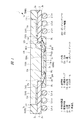
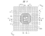
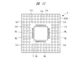
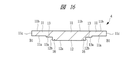
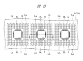
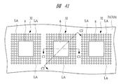
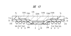
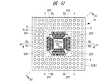
図1および図2は、本発明の一実施の形態である半導体装置1の断面図(側面断面図)であり、図3および図4は、半導体装置1の要部断面図(部分拡大断面図)であり、図5は、半導体装置1の上面図(平面図)であり、図6は、半導体装置1の下面図(底面図、裏面図、平面図)である。図7は、封止部7を透視したときの半導体装置1の上面側の平面透視図(上面図)であり、図8は、封止部8を透視したときの半導体装置1の下面側の平面透視図(下面図)である。図9は、図8において、更にボンディングワイヤBWを外した(透視した)状態の半導体装置1の平面透視図(下面図)である。図10は、図9において、更に半導体チップ5を外した(透視した)状態の半導体装置1の平面透視図(下面図)である。なお、図5〜図10のA1−A1線の断面が図1にほぼ対応し、図5〜図10のA2−A2線の断面が図2にほぼ対応する。また、図3は、図1において、円で囲まれた領域RG1の部分拡大図に対応し、図4は、図2において、円で囲まれた領域RG2の部分拡大図に対応する。図11は、本実施の形態の半導体装置1に使用されている配線基板2の上面図(平面図)であり、図12は、本実施の形態の半導体装置1に使用されている配線基板2の下面図(平面図)である。図13は、本実施の形態の半導体装置1に使用されている放熱板4の上面図(平面図)であり、図14は、本実施の形態の半導体装置1に使用されている放熱板4の下面図(平面図)であり、図15は、本実施の形態の半導体装置1に使用されている放熱板4の側面図であり、図16および図17は、本実施の形態の半導体装置1に使用されている放熱板4の断面図(側面断面図)である。なお、図13および図14のB1−B1線の断面が図16にほぼ対応し、図13および図14のB2−B2線の断面が図17にほぼ対応するが、図13および図14のB1−B1線の位置は、上記図5〜図10のA1−A1線の位置に対応しており、図13および図14のB2−B2線の位置は、上記図5〜図10のA2−A2線の位置に対応している。従って、図16は図1と同じ断面が示され、図17は図2と同じ断面が示されていることになる。また、理解を簡単にするために、図7において、封止部7を透視しても放熱板4で隠れて見えない貫通孔3の位置を点線で示してあり、また、図8において、透視した封止部8の外形位置を点線で示してある。
<Structure of semiconductor device>
1 and 2 are cross-sectional views (side cross-sectional views) of a semiconductor device 1 according to an embodiment of the present invention. FIGS. 3 and 4 are main-portion cross-sectional views (partially enlarged cross-sectional views) of the semiconductor device 1. FIG. 5 is a top view (plan view) of the semiconductor device 1, and FIG. 6 is a bottom view (bottom view, back view, plan view) of the semiconductor device 1. FIG. 7 is a plan perspective view (top view) of the upper surface side of the semiconductor device 1 when the sealing portion 7 is seen through. FIG. 8 is a bottom perspective view of the semiconductor device 1 when the sealing portion 8 is seen through. It is a plane perspective view (bottom view). FIG. 9 is a plan perspective view (bottom view) of the semiconductor device 1 in a state where the bonding wire BW is further removed (seen through) in FIG. FIG. 10 is a plan perspective view (bottom view) of the semiconductor device 1 with the semiconductor chip 5 further removed (seen through) in FIG. 9. 5 to FIG. 10 substantially corresponds to FIG. 1, and the cross section of FIG. 5 to FIG. 10 corresponds to FIG. 3 corresponds to a partially enlarged view of a region RG1 surrounded by a circle in FIG. 1, and FIG. 4 corresponds to a partially enlarged view of a region RG2 surrounded by a circle in FIG. FIG. 11 is a top view (plan view) of the wiring board 2 used in the semiconductor device 1 of the present embodiment. FIG. 12 shows the wiring board 2 used in the semiconductor device 1 of the present embodiment. It is a bottom view (plan view). FIG. 13 is a top view (plan view) of the heat sink 4 used in the semiconductor device 1 of the present embodiment, and FIG. 14 shows the heat sink 4 used in the semiconductor device 1 of the present embodiment. FIG. 15 is a side view of the heat sink 4 used in the semiconductor device 1 of the present embodiment, and FIGS. 16 and 17 are the semiconductor device of the present embodiment. It is sectional drawing (side sectional drawing) of the heat sink 4 currently used for 1. FIG. The cross section taken along line B1-B1 in FIGS. 13 and 14 substantially corresponds to FIG. 16, and the cross section taken along line B2-B2 in FIGS. 13 and 14 substantially corresponds to FIG. 17, but B1 in FIGS. The position of the -B1 line corresponds to the position of the A1-A1 line in FIGS. 5 to 10, and the position of the B2-B2 line in FIGS. 13 and 14 is the position of A2-A2 in FIGS. Corresponds to the position of the line. Therefore, FIG. 16 shows the same cross section as FIG. 1, and FIG. 17 shows the same cross section as FIG. In order to facilitate understanding, in FIG. 7, the positions of the through holes 3 that are hidden by the heat radiating plate 4 even when seen through the sealing portion 7 are shown by dotted lines. In FIG. The outline position of the sealed portion 8 is indicated by a dotted line.

図1〜図10に示される本実施の形態の半導体装置1は、樹脂封止型の半導体パッケージ形態の半導体装置である。   The semiconductor device 1 of the present embodiment shown in FIGS. 1 to 10 is a semiconductor device in the form of a resin-encapsulated semiconductor package.

本実施の形態の半導体装置1は、配線基板2と、配線基板2の貫通孔3内に一部(凸部12)が挿入された放熱板4と、放熱板4の凸部12上に搭載された半導体チップ5と、半導体チップ5の複数の電極パッドPDと配線基板2の複数のボンディングリードBLとを電気的に接続する複数のボンディングワイヤBWとを有している。そして、半導体装置1は、更に、配線基板2の上面2aの一部を覆う封止部7と、半導体チップ5およびボンディングワイヤBWを含む配線基板2の下面2bの一部を覆う封止部8と、配線基板2の下面2bに設けられた複数の半田ボール9とを有している。   The semiconductor device 1 according to the present embodiment is mounted on the wiring board 2, the heat sink 4 in which a part (the convex portion 12) is inserted in the through hole 3 of the wiring substrate 2, and the convex portion 12 of the heat sink 4. And a plurality of bonding wires BW for electrically connecting the plurality of electrode pads PD of the semiconductor chip 5 and the plurality of bonding leads BL of the wiring substrate 2. The semiconductor device 1 further includes a sealing portion 7 that covers a part of the upper surface 2a of the wiring substrate 2 and a sealing portion 8 that covers a part of the lower surface 2b of the wiring substrate 2 including the semiconductor chip 5 and the bonding wires BW. And a plurality of solder balls 9 provided on the lower surface 2 b of the wiring board 2.

図1〜図12に示される配線基板(基板、パッケージ基板、パッケージ用配線基板)2は、一方の主面である上面(表面)2aと、上面2aとは反対側の主面である下面(裏面)2bとを有している。半導体装置1を後述の実装基板21などに実装する際には、配線基板2の下面2b側が実装面(後述の実装基板21に対向する側の面)となるため、配線基板2の下面2bを実装面とみなすこともできる。配線基板2の上面2aと下面2bとは、略平行である。配線基板2の中央部付近には、配線基板2の上面2aから下面2bに到達する貫通孔(孔部、開口部)3が設けられている。   A wiring substrate (substrate, package substrate, package wiring substrate) 2 shown in FIGS. 1 to 12 has an upper surface (front surface) 2a which is one main surface and a lower surface (main surface opposite to the upper surface 2a). Back surface) 2b. When the semiconductor device 1 is mounted on a mounting substrate 21 described later, the lower surface 2b side of the wiring substrate 2 serves as a mounting surface (a surface facing the mounting substrate 21 described later). It can also be regarded as a mounting surface. The upper surface 2a and the lower surface 2b of the wiring board 2 are substantially parallel. Near the center of the wiring board 2, a through hole (hole, opening) 3 that reaches the lower surface 2 b from the upper surface 2 a of the wiring substrate 2 is provided.

図1〜図10および図13〜図17に示される放熱板(放熱用部材、熱伝導部材、ヒートスプレッダ)4は、配線基板2の上面2aに対向する主面11aを有する基材部11と、この基材部11の主面11aにおける中央部に位置し、かつ基材部11から突出する凸部12と、基材部11の主面11aに形成され、かつ配線基板2の上面2aと接触する支持部13とを一体的に有している。放熱板4は、凸部12が貫通孔3内に位置するように、配線基板2の上面2aに配置されて固定されている。   1 to FIG. 10 and FIG. 13 to FIG. 17 are heat radiation plates (heat radiation members, heat conduction members, heat spreaders) 4, a base material portion 11 having a main surface 11 a facing the upper surface 2 a of the wiring substrate 2, The convex part 12 which is located in the central part of the main surface 11a of the base material part 11 and protrudes from the base material part 11 is formed on the main surface 11a of the base material part 11 and is in contact with the upper surface 2a of the wiring board 2. And a support portion 13 to be integrated. The heat sink 4 is arranged and fixed on the upper surface 2 a of the wiring board 2 so that the convex portion 12 is located in the through hole 3.

放熱板4の基材部(ベース部、平板部、放熱部)11は、平板状であり、配線基板2の上面2aに対向する主面11aと、主面11aとは反対側の主面である裏面11bとを有している。この基材部11の裏面11bが封止部7(の上面7a)から露出しており、放熱板4の露出面(放熱面、放熱部)となっている。基材部11の裏面11bはほぼ平坦とすることができる。基材部11の側面11cは、封止部7で覆われている。放熱板4の基材部11は、大きくするほど、放熱性を向上することができる。   A base material portion (base portion, flat plate portion, heat dissipation portion) 11 of the heat radiating plate 4 has a flat plate shape, a main surface 11a facing the upper surface 2a of the wiring board 2 and a main surface opposite to the main surface 11a. And a certain back surface 11b. The back surface 11b of this base material part 11 is exposed from the sealing part 7 (the upper surface 7a), and serves as an exposed surface (heat radiation surface, heat radiation part) of the heat radiating plate 4. The back surface 11b of the base material part 11 can be made substantially flat. The side surface 11 c of the base material part 11 is covered with the sealing part 7. The larger the base material portion 11 of the heat radiating plate 4 is, the more heat radiation can be improved.

基材部11の主面11aの中央付近に、この主面11aに対して略垂直に突出する凸部(突出部、チップ搭載部)12が形成されている。そして、この凸部12は、配線基板2の貫通孔3内に配置(挿入)されている。さらに、この凸部12の主面(表面)12aに半導体チップ5が搭載されている。このため、放熱板4の凸部12を、チップ搭載部とみなすこともできる。すなわち、配線基板2の下面2b側において、配線基板2の貫通孔3内に配置された放熱板4の凸部12上に半導体チップ5が搭載(ダイボンディング)されているため、半導体チップ5は配線基板2の下面2b側に配置された状態となっている。   Near the center of the main surface 11a of the base material part 11, a convex part (protruding part, chip mounting part) 12 that protrudes substantially perpendicular to the main surface 11a is formed. The convex portion 12 is disposed (inserted) in the through hole 3 of the wiring board 2. Further, the semiconductor chip 5 is mounted on the main surface (front surface) 12 a of the convex portion 12. For this reason, the convex part 12 of the heat sink 4 can also be regarded as a chip mounting part. That is, since the semiconductor chip 5 is mounted (die bonding) on the convex portion 12 of the heat sink 4 disposed in the through hole 3 of the wiring substrate 2 on the lower surface 2b side of the wiring substrate 2, the semiconductor chip 5 is The wiring board 2 is disposed on the lower surface 2b side.

また、凸部12は、配線基板2の貫通孔3内に配置されるため、基材部11の主面11aにおいて、配線基板2の貫通孔3と平面的に重なる(内包される)位置に設けられている。一方、支持部13は、配線基板2の貫通孔3外に位置して配線基板2の上面2aに接触するため、基材部11の主面11aにおいて、配線基板2の貫通孔3と平面的に重ならない位置に設けられている。ここで、「平面的に重なる」、「平面的に重ならない」あるいは「平面的に見る」などというときは、配線基板2の上面2aまたは下面2bに平行な平面で見た(投影して見た)場合を言うものとする。   Moreover, since the convex part 12 is arrange | positioned in the through-hole 3 of the wiring board 2, in the main surface 11a of the base material part 11, it is in the position which overlaps with the through-hole 3 of the wiring board 2 planarly (it is included). Is provided. On the other hand, since the support portion 13 is located outside the through hole 3 of the wiring board 2 and contacts the upper surface 2a of the wiring board 2, the support portion 13 is planar with the through hole 3 of the wiring board 2 on the main surface 11a. It is provided at a position that does not overlap. Here, when “overlap in plane”, “does not overlap in plane”, “view in plane”, etc., it is viewed in a plane parallel to the upper surface 2a or the lower surface 2b of the wiring board 2 (projected and viewed). We shall say the case.

半導体装置1において、放熱板4の基材部11の主面11aと配線基板2の上面2aとは、略平行である。また、放熱板4の凸部12は、主面(チップ搭載面)12aおよび側面(側壁)12bを有しており、凸部12の主面12aは凸部12の側面12bで囲まれている。言い換えると、凸部12の側面12bは、凸部12の主面12aと基材部11の主面11aとの間に位置している。放熱板4の凸部12の主面12aは、基材部11の主面11aと略平行であるため、配線基板2の下面2bとも略平行となっている。また、平面的に見ると、凸部12は基材部11に平面的に内包されている。半導体チップ5は、凸部12の主面12aに接合材(接着材、ダイボンディング材)14を介して接合されて固定されている。凸部12の側面12bは、配線基板2の貫通孔3の内壁に対向している。   In the semiconductor device 1, the main surface 11 a of the base material portion 11 of the heat sink 4 and the upper surface 2 a of the wiring substrate 2 are substantially parallel. Further, the convex portion 12 of the heat sink 4 has a main surface (chip mounting surface) 12 a and a side surface (side wall) 12 b, and the main surface 12 a of the convex portion 12 is surrounded by the side surface 12 b of the convex portion 12. . In other words, the side surface 12 b of the convex portion 12 is located between the main surface 12 a of the convex portion 12 and the main surface 11 a of the base material portion 11. The main surface 12 a of the convex portion 12 of the heat radiating plate 4 is substantially parallel to the main surface 11 a of the base material portion 11, and thus is also substantially parallel to the lower surface 2 b of the wiring board 2. Further, when viewed in a plan view, the convex portion 12 is included in the base material portion 11 in a plan view. The semiconductor chip 5 is bonded and fixed to the main surface 12 a of the convex portion 12 via a bonding material (adhesive material, die bonding material) 14. The side surface 12 b of the convex portion 12 faces the inner wall of the through hole 3 of the wiring board 2.

凸部12の側面12bは、基材部11の主面11aに対して略垂直である。但し、後述のように、半導体装置1の製造工程(後述のステップS6に対応する工程)で凸部12の溝16を押し広げて放熱板4(の凸部12)を配線基板2(具体的には後述の配線基板31)にかしめたため、図3に模式的に示されるように、凸部12の側面12bのうち、主面11aに近い領域は、配線基板2の貫通孔3の内壁に近づく側に変形(傾斜)して配線基板2の貫通孔3の内壁に接している。このため、後述のステップS6のかしめ工程を行う前の段階では、放熱板12の凸部12の側面12b全体が、基材部11の主面11aに対して略垂直であり、凸部12の側面12bのうちの主面11aに近い領域も変形(傾斜)していない(後述の図49参照)。   The side surface 12 b of the convex portion 12 is substantially perpendicular to the main surface 11 a of the base material portion 11. However, as will be described later, in the manufacturing process of the semiconductor device 1 (a process corresponding to step S6 described later), the groove 16 of the convex portion 12 is expanded and the heat sink 4 (the convex portion 12) is connected to the wiring board 2 (specifically. Therefore, the region near the main surface 11a of the side surface 12b of the convex portion 12 is formed on the inner wall of the through hole 3 of the wiring substrate 2 as schematically shown in FIG. It is deformed (inclined) toward the approaching side and is in contact with the inner wall of the through hole 3 of the wiring board 2. For this reason, in the stage before performing the caulking process of step S6 described later, the entire side surface 12b of the convex portion 12 of the heat radiating plate 12 is substantially perpendicular to the main surface 11a of the base material portion 11, and The region of the side surface 12b close to the main surface 11a is not deformed (inclined) (see FIG. 49 described later).

基材部11の主面11aに設けられた支持部13は、配線基板2の上面2aに接する支持面13aを有している。この支持面13aは平坦面とすることができる。基材部11の主面11aと支持部13の支持面13aと凸部12の主面12aとは、互いに高さ位置が異なり、基材部11の主面11aを基準にすると、支持部13の支持面13aは、基材部11の主面11aよりも高い位置にあり、凸部12の主面12aは、基材部11の主面11aおよび支持部13の支持面13aよりも更に高い位置にある(ここでは基材部11の主面11aから凸部12の主面12a側を高さが高い方向としている)。換言すれば、支持部13(の支持面13a)は、凸部12(の主面12a)よりも低く、基材部11の主面11a(凸部12と支持部13のいずれも形成されていない領域)は、支持部13(の支持面13a)よりも低くなっている。   The support portion 13 provided on the main surface 11 a of the base material portion 11 has a support surface 13 a in contact with the upper surface 2 a of the wiring board 2. The support surface 13a can be a flat surface. The main surface 11 a of the base material part 11, the support surface 13 a of the support part 13, and the main surface 12 a of the convex part 12 have different height positions, and the support part 13 is based on the main surface 11 a of the base material part 11. The support surface 13a is higher than the main surface 11a of the base material portion 11, and the main surface 12a of the convex portion 12 is higher than the main surface 11a of the base material portion 11 and the support surface 13a of the support portion 13. It is in a position (here, the main surface 12a side of the convex portion 12 from the main surface 11a of the base material portion 11 is set to a height direction). In other words, the support portion 13 (the support surface 13a thereof) is lower than the convex portion 12 (the main surface 12a thereof), and the main surface 11a (the convex portion 12 and the support portion 13) of the base material portion 11 is formed. The non-region) is lower than the support portion 13 (the support surface 13a).

このため、配線基板2の貫通孔3内に凸部12が配置(挿入)され、配線基板2の上面2aに支持部13の支持面13aが接し、基材部11の主面11aにおける凸部12と支持部13のいずれも設けられていない領域は、配線基板2の上面2aから離間した状態となっている。従って、基材部11の主面11aにおける凸部12と支持部13のいずれも設けられていない領域と配線基板2の上面2aとの間には、隙間(隙間部)18が形成されており、この隙間18には、封止部7の一部(すなわち封止部7用の樹脂材料MR)が充填されている。   Therefore, the convex portion 12 is disposed (inserted) in the through hole 3 of the wiring board 2, the support surface 13 a of the support portion 13 is in contact with the upper surface 2 a of the wiring substrate 2, and the convex portion on the main surface 11 a of the base material portion 11. The region where neither 12 nor the support portion 13 is provided is in a state of being separated from the upper surface 2 a of the wiring board 2. Therefore, a gap (gap portion) 18 is formed between the region of the main surface 11 a of the base material portion 11 where neither the convex portion 12 nor the support portion 13 is provided and the upper surface 2 a of the wiring board 2. The gap 18 is filled with a part of the sealing portion 7 (that is, the resin material MR for the sealing portion 7).

このように、貫通孔3の外部で配線基板2の上面2a側に位置する基材部11と、配線基板2の貫通孔3内に配置(挿入)されている凸部12と、配線基板2の上面2aに接触して基材部11の主面11aと配線基板2の上面2aとの間を離間させる(すなわち基材部11の主面11aと配線基板2の上面2aとの間に隙間18を形成する)ための支持部13とが一体的に形成されて、放熱板4を構成している。   Thus, the base material part 11 located on the upper surface 2a side of the wiring board 2 outside the through hole 3, the convex part 12 disposed (inserted) in the through hole 3 of the wiring board 2, and the wiring board 2 The main surface 11a of the base material part 11 and the upper surface 2a of the wiring board 2 are separated from each other in contact with the upper surface 2a (that is, there is a gap between the main surface 11a of the base material part 11 and the upper surface 2a of the wiring board 2). And the support portion 13 for forming the heat sink 18 are integrally formed to constitute the heat radiating plate 4.

凸部12の主面12aが、チップ搭載面(半導体チップ5を搭載する面)であり、放熱板4のチップ搭載面(すなわち凸部12の主面12a)は、配線基板2の下面2bと略同一平面上にある。これは、支持面13の支持面13aと凸部12の主面12aとの高低差(高さの差)を、配線基板2の厚み(すなわち配線基板2の上面2aと下面2bとの高低差)とほぼ同じにすることで実現できる。   The main surface 12 a of the convex portion 12 is a chip mounting surface (surface on which the semiconductor chip 5 is mounted), and the chip mounting surface of the heat sink 4 (that is, the main surface 12 a of the convex portion 12) is connected to the lower surface 2 b of the wiring board 2. It is on substantially the same plane. This is because the difference in height (height difference) between the support surface 13a of the support surface 13 and the main surface 12a of the convex portion 12 is the difference in height between the thickness of the wiring board 2 (that is, the upper surface 2a and the lower surface 2b of the wiring board 2). ) Can be realized by almost the same.

放熱板4は、チップ搭載用の導体部(金属部)と、放熱用の導体部(金属部)とを兼ねたものである。配線基板2の貫通孔3内に凸部12が配置されるように配線基板2の上面2a側に放熱板4を配置し、この放熱板4の凸部12上に半導体チップ5を配置することで、半導体装置1の使用時に半導体チップ5で生じた熱を放熱板4に伝導させ、放熱板4の露出部(基材部11の裏面11b)から半導体装置1の外部に放熱することができる。   The heat radiating plate 4 serves as both a chip mounting conductor (metal part) and a heat radiating conductor (metal part). The heat sink 4 is disposed on the upper surface 2 a side of the wiring board 2 so that the convex portion 12 is disposed in the through hole 3 of the wiring substrate 2, and the semiconductor chip 5 is disposed on the convex portion 12 of the heat sink 4. Thus, heat generated in the semiconductor chip 5 when the semiconductor device 1 is used can be conducted to the heat radiating plate 4 and radiated from the exposed portion of the heat radiating plate 4 (the back surface 11b of the base material portion 11) to the outside of the semiconductor device 1. .

放熱板4は、半導体チップ5で生じた熱を放熱するための部材であるため、熱伝導性が高いことが好ましく、少なくとも配線基板2および封止部7,8の熱伝導性(熱伝導率)よりも放熱板4の熱伝導性(熱伝導率)が高いことが必要である。導電性材料(特に金属材料)は熱伝導性も高いため、放熱板4は、導電性材料からなることが好ましく、金属材料で形成されていればより好ましい。放熱板4に、銅(Cu)または銅(Cu)合金のような銅(Cu)を主成分とする金属材料を用いれば、放熱板4の高い熱伝導性を得られ、加工(放熱板4の形成)もしやすいので、更に好ましい。   Since the heat radiating plate 4 is a member for radiating the heat generated in the semiconductor chip 5, it is preferable that the heat radiating plate 4 has high thermal conductivity, and at least the thermal conductivity (thermal conductivity of the wiring substrate 2 and the sealing portions 7 and 8. ) Is required to have a higher thermal conductivity (thermal conductivity). Since the conductive material (particularly metal material) has high thermal conductivity, the heat sink 4 is preferably made of a conductive material, and more preferably formed of a metal material. If a metal material mainly composed of copper (Cu) such as copper (Cu) or a copper (Cu) alloy is used for the heat sink 4, high heat conductivity of the heat sink 4 can be obtained and processed (heat sink 4 Is more preferable.

配線基板2の貫通孔3と、貫通孔内3に位置する凸部12とは、配線基板2の上面2aに平行な断面形状がほぼ同じであり、凸部12の側面12bは、一部が配線基板2の貫通孔3の内壁(側壁、側面)と直接的に接触(密着)している。しかしながら、チップ搭載部12の側面12bの全面が配線基板2の貫通孔3の内壁に直接的に接触(密着)している訳ではない。   The through hole 3 of the wiring board 2 and the convex part 12 located in the through hole 3 have substantially the same cross-sectional shape parallel to the upper surface 2a of the wiring board 2, and the side surface 12b of the convex part 12 is partially The wiring board 2 is in direct contact (adhesion) with the inner wall (side wall, side surface) of the through hole 3. However, the entire side surface 12 b of the chip mounting portion 12 is not in direct contact (adherence) to the inner wall of the through hole 3 of the wiring board 2.

すなわち、配線基板2の貫通孔3の内壁と凸部12の側面12bとの間における少なくとも一箇所(好ましくは複数個所)に、貫通孔3の内壁と凸部12の側面12bとが離間しかつ配線基板2の上面2a側から下面2b側まで繋がる(連通する、貫通する)隙間部15がある。そして、この隙間部15は、封止部7,8と一体的に形成された樹脂材料で充填されている(満たされている)。   That is, the inner wall of the through hole 3 and the side surface 12b of the convex portion 12 are spaced apart from each other at least at one location (preferably a plurality of locations) between the inner wall of the through hole 3 of the wiring substrate 2 and the side surface 12b of the convex portion 12. There is a gap portion 15 that is connected (communicated or penetrates) from the upper surface 2a side to the lower surface 2b side of the wiring board 2. The gap portion 15 is filled (filled) with a resin material formed integrally with the sealing portions 7 and 8.

凸部12および貫通孔3の平面形状は、種々の形状とすることができるが、矩形状(略矩形)であればより好ましい。図1〜図17には、凸部12および貫通孔3の平面形状を矩形状とした場合が示されている。但し、上記隙間部15を形成可能とするために、凸部12の平面形状と貫通孔3の平面形状とを完全に一致させるのではなく、凸部12の平面形状に比べて貫通孔3の平面形状を局所的に大きくするか、あるいは、貫通孔3の平面形状に比べて凸部12の平面形状を局所的に小さくする。   Although the planar shape of the convex part 12 and the through-hole 3 can be made into various shapes, if it is a rectangular shape (substantially rectangular), it is more preferable. The case where the planar shape of the convex part 12 and the through-hole 3 was made into the rectangular shape is shown by FIGS. However, in order to be able to form the gap portion 15, the planar shape of the convex portion 12 and the planar shape of the through hole 3 are not completely matched, but the through hole 3 is compared with the planar shape of the convex portion 12. The planar shape is locally increased or the planar shape of the convex portion 12 is locally reduced as compared with the planar shape of the through hole 3.

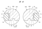
例えば、図11および図12に示されるように、配線基板2における貫通孔3の平面形状を、四隅が略直角の矩形としておき、一方、図14に示されるように、凸部12の平面形状は、矩形状であるが、四隅が完全に直角の矩形ではなく矩形の四隅において角を落した形状とする。あるいは、配線基板2における貫通孔3の平面形状を、矩形状であるが、四隅が完全に直角の矩形ではなく矩形の四隅において角を局所的に広げた形状にしておき、一方、凸部12の平面形状は四隅が略直角の矩形としてもよい。ここで、貫通孔3の平面形状は、配線基板2の上面2aまたは下面2bに平行な平面での形状であり、凸部12の平面形状は、基材部11の主面11aまたは凸部12の主面12aに平行な平面での形状に対応する。また、図14の構成例をより具体的に説明すると、図14の符号17で示した四隅(凸部12の平面形状を構成する矩形の四隅)において、平面形状(凸部12の主面に平行な平面での形状)が例えば円の約1/4(四半円)で、かつ凸部12の側面12bに沿って凸部12の主面12aから基材部11の主面11aまで延在する溝を形成している。   For example, as shown in FIG. 11 and FIG. 12, the planar shape of the through hole 3 in the wiring board 2 is set to a rectangle with four corners having substantially right angles, while the planar shape of the convex portion 12 as shown in FIG. Is a rectangular shape, but the corners are not completely rectangular at right angles, but have a shape with corners dropped at the four corners of the rectangle. Alternatively, the planar shape of the through-hole 3 in the wiring board 2 is a rectangular shape, but the corners are not completely rectangular at right angles, but are formed such that the corners are locally widened at the four corners of the rectangle, while the convex portion 12 The planar shape may be a rectangle whose four corners are substantially perpendicular. Here, the planar shape of the through-hole 3 is a shape in a plane parallel to the upper surface 2 a or the lower surface 2 b of the wiring substrate 2, and the planar shape of the convex portion 12 is the main surface 11 a or the convex portion 12 of the base material portion 11. This corresponds to a shape in a plane parallel to the main surface 12a. Further, the configuration example of FIG. 14 will be described more specifically. At the four corners (rectangular four corners constituting the planar shape of the convex portion 12) indicated by reference numeral 17 in FIG. The shape in a parallel plane) is, for example, about 1/4 of a circle (quarter circle), and extends from the main surface 12a of the convex portion 12 to the main surface 11a of the base material portion 11 along the side surface 12b of the convex portion 12. Grooves are formed.

このようにすることで、放熱板4の凸部12が配線基板2の貫通孔3内に配置(挿入)されると、矩形(凸部12および貫通孔3の平面形状を構成する矩形)の四隅近傍以外では凸部12の側面12bと配線基板2の貫通孔3の内壁とが近接するが、それに比べて、矩形の四隅近傍では、凸部12の側面12bと配線基板2の貫通孔3の内壁との間が離間し、矩形の四隅近傍に隙間部15が生じる。   By doing in this way, when the convex part 12 of the heat sink 4 is arranged (inserted) in the through hole 3 of the wiring board 2, it is rectangular (rectangular that forms the planar shape of the convex part 12 and the through hole 3). The side surface 12b of the convex portion 12 and the inner wall of the through hole 3 of the wiring board 2 are close to each other except near the four corners. However, the side surface 12b of the convex portion 12 and the through hole 3 of the wiring substrate 2 are near the four corners of the rectangle. Are spaced apart from each other and gaps 15 are formed in the vicinity of the four corners of the rectangle.

この隙間部15は、後述のステップS5,S6で放熱板4の凸部12を貫通孔3内に配置(挿入)して固定した(かしめた)段階で、凸部12の側面12bと貫通孔3の内壁との間に形成される。そして、封止部7,8を形成する前は、この隙間部15は空洞であり、隙間部15に樹脂材料MRは充填されていない状態となっており、封止部7,8を形成する際に、隙間部15は樹脂材料MRの流路なるとともに、樹脂材料MRが充填される。   This gap 15 is formed at the stage where the projection 12 of the heat sink 4 is placed (inserted) in the through-hole 3 and fixed (caulked) in steps S5 and S6, which will be described later. 3 and the inner wall. Before the sealing portions 7 and 8 are formed, the gap portion 15 is hollow, and the gap portion 15 is not filled with the resin material MR, and the sealing portions 7 and 8 are formed. At this time, the gap 15 becomes a flow path of the resin material MR and is filled with the resin material MR.

すなわち、詳細は後述するが、封止部7,8を形成する際に(後述のステップS8のモールド工程に対応)、封止部7,8形成用の樹脂材料MRを配線基板2の上面2a側に供給し、この樹脂材料MRを上記隙間8とこの隙間部15とを通じて配線基板2の下面2b側にも供給し、それによって配線基板2の上面2aおよび下面2bに封止部7および封止部8を形成している。このため、各隙間部15は、封止部7,8形成時に封止部7,8形成用の樹脂材料MRが流れることができる程度の寸法とされ、配線基板2の上面2a側から下面2b側まで連続的に延在して繋がっている(貫通している)。従って、各隙間部15は、配線基板2の上面2a側では、基材部11の主面11aと配線基板2の上面2aとの間の上記隙間18と繋がり、配線基板2の下面2b側では、封止部8と繋がっている。そして、封止部7と封止部8とは、同じ樹脂材料MRにより形成されており、これと同じ樹脂材料MRが、隙間18および隙間部15内を充填している(満たしている)。すなわち、封止部7と封止部8とは、隙間部15内を満たす樹脂材料MRを介して一体的に繋がった状態となっている。   That is, although details will be described later, when forming the sealing portions 7 and 8 (corresponding to a molding process in step S8 described later), the resin material MR for forming the sealing portions 7 and 8 is used as the upper surface 2a of the wiring board 2. The resin material MR is also supplied to the lower surface 2b side of the wiring board 2 through the gap 8 and the gap portion 15, whereby the sealing portion 7 and the sealing are formed on the upper surface 2a and the lower surface 2b of the wiring substrate 2. A stop 8 is formed. For this reason, each gap portion 15 has such a dimension that the resin material MR for forming the sealing portions 7 and 8 can flow when the sealing portions 7 and 8 are formed, and the lower surface 2b from the upper surface 2a side of the wiring board 2. It extends continuously to the side and is connected (penetrated). Accordingly, each gap portion 15 is connected to the gap 18 between the main surface 11a of the base material portion 11 and the upper surface 2a of the wiring board 2 on the upper surface 2a side of the wiring board 2 and on the lower surface 2b side of the wiring board 2. , Connected to the sealing portion 8. The sealing portion 7 and the sealing portion 8 are formed of the same resin material MR, and the same resin material MR fills (fills) the gap 18 and the gap portion 15. That is, the sealing portion 7 and the sealing portion 8 are integrally connected through the resin material MR filling the gap portion 15.

また、放熱板4の凸部12の主面12aには、溝(凹部、窪み部)16が形成されている。この溝16は、凸部12の主面12aの周辺部(外周部)に形成されており、半導体チップ5は、凸部12の主面12aにおいて、溝16が形成されている領域よりも中央側に搭載されている。すなわち、凸部12の主面12aにおいて、溝16は、半導体チップ5が搭載されている領域よりも外周側に形成されている。凸部12の主面12aにおいて、溝16は、主面12aの各辺に沿って形成されていることが好ましく、図14に示されるように、主面12aが矩形状である場合には、四隅近傍を除いて主面12aの四辺に沿って形成されていることが好ましい。   Further, a groove (concave portion, recessed portion) 16 is formed on the main surface 12 a of the convex portion 12 of the heat radiating plate 4. The groove 16 is formed in the peripheral portion (outer peripheral portion) of the main surface 12 a of the convex portion 12, and the semiconductor chip 5 is located on the main surface 12 a of the convex portion 12 in the center of the region where the groove 16 is formed. It is mounted on the side. That is, in the main surface 12a of the convex portion 12, the groove 16 is formed on the outer peripheral side with respect to the region where the semiconductor chip 5 is mounted. In the main surface 12a of the convex portion 12, the groove 16 is preferably formed along each side of the main surface 12a. As shown in FIG. 14, when the main surface 12a is rectangular, It is preferably formed along the four sides of the main surface 12a except for the vicinity of the four corners.

溝16は、半導体装置1の製造時に、放熱板4(の凸部12)と配線基板2とをかしめて、固定するために用いたものである。すなわち、半導体装置1の製造時に配線基板2の貫通孔3内に放熱板4の凸部12を挿入した後、後述の治具46などで凸部12の主面12aの溝16を押し広げることで、放熱板4(の凸部12)と配線基板2とを、かしめて、固定している。凸部12の主面12aの溝16を押し広げると、溝16が押し広げられた体積分だけ、水平方向に凸部12の一部が広がり、凸部12の側面12bの一部を配線基板2の貫通孔3の内壁に接触(密着)させることができる。その反作用により、配線基板2の貫通孔3の内壁が凸部12の側面12bの一部に密着して押すような力を作用させ、それによって、放熱板4(の凸部12)と配線基板2とを、かしめることができ、放熱板4を配線基板2に固定することができる。これにより、封止部7,8を形成するまで、放熱板4を配線基板2に固定することができ、半導体装置1の製造が容易になる。   The groove 16 is used for caulking and fixing the heat radiating plate 4 (projection 12 thereof) and the wiring board 2 when the semiconductor device 1 is manufactured. That is, after the protrusion 12 of the heat sink 4 is inserted into the through-hole 3 of the wiring board 2 when the semiconductor device 1 is manufactured, the groove 16 of the main surface 12a of the protrusion 12 is expanded with a jig 46 described later. Thus, the heat radiating plate 4 (projection 12 thereof) and the wiring board 2 are caulked and fixed. When the groove 16 of the main surface 12a of the convex portion 12 is expanded, a part of the convex portion 12 expands in the horizontal direction by the volume of the groove 16 that is expanded, and a part of the side surface 12b of the convex portion 12 is formed on the wiring board. It is possible to make contact (contact) with the inner wall of the two through holes 3. Due to the reaction, a force is applied so that the inner wall of the through hole 3 of the wiring board 2 is in close contact with and pressed against a part of the side surface 12b of the convex part 12, thereby causing the heat sink 4 (the convex part 12) and the wiring board to be pressed. 2 can be caulked, and the heat sink 4 can be fixed to the wiring board 2. Thereby, the heat sink 4 can be fixed to the wiring board 2 until the sealing portions 7 and 8 are formed, and the manufacture of the semiconductor device 1 is facilitated.

半導体チップ5は、その厚さと交差する平面形状が矩形(四角形)であり、例えば、単結晶シリコンなどからなる半導体基板(半導体ウエハ)の主面に種々の半導体素子または半導体集積回路などを形成した後、必要に応じて半導体基板の裏面研削を行ってから、ダイシングなどにより半導体基板を各半導体チップ5に分離したものである。半導体チップ5は、互いに反対側に位置する2つの主面である表面(半導体素子形成側の主面、上面)5aおよび裏面(表面とは反対側の主面、下面)5bを有しており、半導体チップ5の表面5aには、複数の電極パッド(電極、ボンディングパッド、パッド電極)PDが形成されている。各電極パッドPDは、半導体チップ5内部または表層部分に形成された半導体素子または半導体集積回路に電気的に接続されている。   The semiconductor chip 5 has a rectangular (quadrangle) planar shape that intersects its thickness. For example, various semiconductor elements or semiconductor integrated circuits are formed on the main surface of a semiconductor substrate (semiconductor wafer) made of single crystal silicon or the like. Thereafter, the back surface of the semiconductor substrate is ground if necessary, and then the semiconductor substrate is separated into the respective semiconductor chips 5 by dicing or the like. The semiconductor chip 5 has a front surface (main surface and upper surface) 5a and a rear surface (main surface and lower surface opposite to the front surface) 5b, which are two main surfaces located on opposite sides. A plurality of electrode pads (electrodes, bonding pads, pad electrodes) PD are formed on the surface 5 a of the semiconductor chip 5. Each electrode pad PD is electrically connected to a semiconductor element or a semiconductor integrated circuit formed in the semiconductor chip 5 or on the surface layer portion.

半導体チップ5は、放熱板4の凸部12にフェイスアップボンディングされており、半導体チップ5の裏面5bが放熱板4の凸部12の主面12aに接合材(接着材、ダイボンディング材)14を介して接着されて固定されている。配線基板2の貫通孔3および放熱板4の凸部12の平面寸法は、それぞれ半導体チップ5の平面寸法よりも大きく、放熱板4の凸部12上に搭載された半導体チップ5は、配線基板2の貫通孔3および放熱板4の凸部12に平面的に内包されるように配置されている。接着材14としては、熱伝導性が高い接着材を用いることが好ましく、例えば半田や導電性のペースト材(導電性のペースト材として好ましいのは銀ペースト)などを用いることができる。   The semiconductor chip 5 is face-up bonded to the convex portion 12 of the heat sink 4 and the back surface 5b of the semiconductor chip 5 is bonded to the main surface 12a of the convex portion 12 of the heat sink 4 with a bonding material (adhesive or die bonding material) 14. It is bonded and fixed through. The planar dimensions of the through-hole 3 of the wiring board 2 and the convex part 12 of the heat sink 4 are larger than the planar dimension of the semiconductor chip 5, and the semiconductor chip 5 mounted on the convex part 12 of the heat sink 4 The two through holes 3 and the protrusions 12 of the heat sink 4 are arranged so as to be included in a plane. As the adhesive 14, it is preferable to use an adhesive having high thermal conductivity. For example, solder or a conductive paste material (preferably a silver paste as the conductive paste material) can be used.

配線基板2は、絶縁性の基材層(絶縁基板、コア材)と、基材層の上面および下面に形成された導体層(導体パターン、導体膜パターン、配線層)とを有している。配線基板2として、1つの絶縁層(基材層)の上面および下面に導体層が形成された基板を用いても、あるいは複数の絶縁層(基材層)と複数の導体層(配線層)とが多層に亘って交互に形成(積層)されて一体化された多層配線基板(多層基板)を用いてもよいが、配線の引き回しを考慮すると、多層配線基板の方が好ましい。図1〜図4では、配線基板2の内部(基材層の層間)の配線層については、図示を省略している。配線基板2の基材層として、例えば、樹脂材料(例えばガラスエポキシ樹脂)などを用いることができる。   The wiring substrate 2 has an insulating base material layer (insulating substrate, core material) and conductor layers (conductor pattern, conductor film pattern, wiring layer) formed on the upper surface and the lower surface of the base material layer. . The wiring board 2 may be a board in which a conductor layer is formed on the upper and lower surfaces of one insulating layer (base material layer), or a plurality of insulating layers (base material layers) and a plurality of conductor layers (wiring layers). Alternatively, a multilayer wiring board (multilayer board) that is alternately formed (laminated) and integrated over multiple layers may be used. However, in consideration of wiring routing, the multilayer wiring board is preferable. In FIG. 1 to FIG. 4, the illustration of the wiring layer inside the wiring board 2 (interlayer of the base material layer) is omitted. As the base material layer of the wiring board 2, for example, a resin material (for example, a glass epoxy resin) or the like can be used.

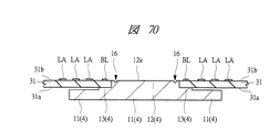
本実施の形態の半導体装置1では、配線基板2の下面2b側(凸部12上)に半導体チップ5を配置し、かつ配線基板2の下面2b側に外部端子(ここでは半田ボール9)を配置している。このため、配線基板2の上面2a側には、端子(ボンディングリード、バンプランド)や配線を構成する導体層がなくともよい。一方、配線基板2の下面2bには、ボンディングワイヤBWを接続するための複数のボンディングリード(電極パッド、接続端子、電極、ボンディングパッド、パッド電極)BLと、バンプ電極である半田ボール9を接続するための複数のバンプランド(電極パッド、導電性ランド、電極、ランド電極、パッド、端子)LAが形成されている。複数のボンディングリードBLおよび複数のバンプランドLAは、導体層の一部から成り、本実施の形態では、例えばめっき法で形成された銅薄膜などの導電性材料により形成することができる。   In the semiconductor device 1 according to the present embodiment, the semiconductor chip 5 is arranged on the lower surface 2b side (on the convex portion 12) of the wiring board 2, and the external terminals (here, solder balls 9) are arranged on the lower surface 2b side of the wiring board 2. It is arranged. For this reason, on the upper surface 2a side of the wiring board 2, there may be no terminals (bonding leads, bump lands) or conductor layers constituting the wiring. On the other hand, a plurality of bonding leads (electrode pads, connection terminals, electrodes, bonding pads, pad electrodes) BL for connecting the bonding wires BW and solder balls 9 as bump electrodes are connected to the lower surface 2b of the wiring board 2. A plurality of bump lands (electrode pads, conductive lands, electrodes, land electrodes, pads, terminals) LA are formed. The plurality of bonding leads BL and the plurality of bump lands LA are formed of a part of a conductor layer, and in this embodiment, can be formed of a conductive material such as a copper thin film formed by plating.

図12に示されるように、複数のボンディングリードBLは、配線基板2の下面2bにおいて、貫通孔3の周囲に配置(形成)されており、複数のバンプランドLAは、配線基板2の下面2bにおいて、複数のボンディングリードBLが配置されている領域の更に周囲に配置(形成)されている。   As shown in FIG. 12, the plurality of bonding leads BL are arranged (formed) around the through hole 3 on the lower surface 2 b of the wiring substrate 2, and the plurality of bump lands LA are formed on the lower surface 2 b of the wiring substrate 2. In FIG. 5, the region is disposed (formed) further around the region where the plurality of bonding leads BL are disposed.

配線基板2において、複数のボンディングリードBLと複数のバンプランドLAとは、配線基板2の配線を介してそれぞれ電気的に接続されている。ここで、各ボンディングリードBLと各バンプランドLAとを電気的に接続する配線には、配線基板2の下面2bの配線層、配線基板2の上面2aの配線層、配線基板2の内部の配線層、配線基板2の異なる配線層間を接続するビア配線などが必要に応じて使用される。また、これらの配線も、ボンディングリードBLおよびバンプランドLAと同様に、配線基板2の導体層の一部から成る。また、図示しないが、必要に応じて、ソルダレジスト層(絶縁層、絶縁膜)を配線基板2の上面2aおよび下面2b上に形成することもでき、この場合、配線基板2の下面2bにおいて、ボンディングリードBLおよびバンプランドLAはソルダレジスト層(の開口部)から露出され、配線基板2の下面2bの配線(ボンディングリードBLおよびバンプランドLA間を結線する配線)はソルダレジスト層で覆われる。配線基板2(31)の上面2a(31a)にソルダレジスト層(絶縁層、絶縁膜)を形成した場合には、そのソルダレジスト層(絶縁層、絶縁膜)の表面を配線基板2(31)の上面2a(31a)とみなすこともでき、放熱板4の支持部13の支持面13aは、そのソルダレジスト層(絶縁層、絶縁膜)の表面に接触することになる。配線基板2(31)の下面2b(31b)にソルダレジスト層(絶縁層、絶縁膜)を形成した場合には、そのソルダレジスト層(絶縁層、絶縁膜)の表面を配線基板2(31)の下面2b(31b)とみなすこともできる。   In the wiring board 2, the plurality of bonding leads BL and the plurality of bump lands LA are electrically connected to each other through the wiring of the wiring board 2. Here, the wiring that electrically connects each bonding lead BL and each bump land LA includes a wiring layer on the lower surface 2b of the wiring substrate 2, a wiring layer on the upper surface 2a of the wiring substrate 2, and a wiring inside the wiring substrate 2. Layers, via wirings connecting different wiring layers of the wiring board 2, and the like are used as necessary. In addition, these wirings are also composed of a part of the conductor layer of the wiring board 2 in the same manner as the bonding leads BL and the bump lands LA. Although not shown, a solder resist layer (insulating layer, insulating film) can be formed on the upper surface 2a and the lower surface 2b of the wiring board 2 as necessary. In this case, on the lower surface 2b of the wiring board 2, The bonding lead BL and the bump land LA are exposed from the solder resist layer (the opening thereof), and the wiring on the lower surface 2b of the wiring substrate 2 (wiring connecting the bonding lead BL and the bump land LA) is covered with the solder resist layer. When a solder resist layer (insulating layer, insulating film) is formed on the upper surface 2a (31a) of the wiring board 2 (31), the surface of the solder resist layer (insulating layer, insulating film) is used as the wiring board 2 (31). The support surface 13a of the support part 13 of the heat sink 4 is in contact with the surface of the solder resist layer (insulating layer, insulating film). When a solder resist layer (insulating layer, insulating film) is formed on the lower surface 2b (31b) of the wiring board 2 (31), the surface of the solder resist layer (insulating layer, insulating film) is used as the wiring board 2 (31). It can also be regarded as the lower surface 2b (31b).

従って、半導体チップ5の複数の電極パッドPDは、複数のボンディングワイヤBWを介して配線基板2の下面2bの複数のボンディングリードBLに電気的に接続され、更に配線基板2の配線などを介して配線基板2の下面2bの複数のバンプランドLA(および複数のバンプランドLAに接続された複数の半田ボール9)に電気的に接続されている。各ボンディングワイヤ(導電性ワイヤ、導電性接続部材)BWは、半導体チップ5の各電極パッドPDと配線基板2の各ボンディングリードBLとを電気的に接続するための導電性接続部材として機能し、好ましくは導電性のワイヤ(接続部材)からなり、例えば金線などの金属細線からなる。   Accordingly, the plurality of electrode pads PD of the semiconductor chip 5 are electrically connected to the plurality of bonding leads BL on the lower surface 2b of the wiring board 2 via the plurality of bonding wires BW, and further via the wiring of the wiring board 2 and the like. The wiring board 2 is electrically connected to a plurality of bump lands LA (and a plurality of solder balls 9 connected to the plurality of bump lands LA) on the lower surface 2b of the wiring board 2. Each bonding wire (conductive wire, conductive connecting member) BW functions as a conductive connecting member for electrically connecting each electrode pad PD of the semiconductor chip 5 and each bonding lead BL of the wiring board 2, Preferably, it consists of a conductive wire (connecting member), for example, a fine metal wire such as a gold wire.

複数のバンプランドLAは、配線基板2の下面2bにおいて、封止部8が配置されていない領域にアレイ状に配置されており、各バンプランドLAに半田ボール(ボール電極、半田バンプ、バンプ電極、突起電極)9が接続されている。このため、配線基板2の下面2bにおいて、封止部8が配置されていない領域に、外部端子として複数の半田ボール9がアレイ状に配置されている。   The plurality of bump lands LA are arranged in an array on the lower surface 2b of the wiring board 2 in the area where the sealing portion 8 is not arranged, and solder balls (ball electrodes, solder bumps, bump electrodes) are arranged on the bump lands LA. , Protruding electrode) 9 is connected. For this reason, on the lower surface 2b of the wiring board 2, a plurality of solder balls 9 are arranged in an array form as external terminals in a region where the sealing portion 8 is not arranged.

半田ボール9が配置された配線基板2の下面2bが、半導体装置1の下面となり、これが半導体装置1の実装面(実装基板に実装する側の主面)となる。従って、本実施の形態の半導体装置1は、BGA(Ball Grid Array package)形態の半導体装置である。半田ボール9は、半田材料からなり、半導体装置の1のバンプ電極(突起電極、半田バンプ)として機能し、半導体装置1の外部端子(外部接続用端子)として機能することができる。このため、配線基板2の複数のバンプランドLA上に複数の外部端子(ここでは半田ボール9)がそれぞれ形成されていると言うことができる。   The lower surface 2b of the wiring board 2 on which the solder balls 9 are arranged becomes the lower surface of the semiconductor device 1, and this becomes the mounting surface (the main surface on the side mounted on the mounting substrate) of the semiconductor device 1. Therefore, the semiconductor device 1 according to the present embodiment is a semiconductor device in the form of a BGA (Ball Grid Array package). The solder ball 9 is made of a solder material, functions as one bump electrode (projection electrode, solder bump) of the semiconductor device, and can function as an external terminal (external connection terminal) of the semiconductor device 1. For this reason, it can be said that a plurality of external terminals (here, solder balls 9) are formed on the plurality of bump lands LA of the wiring board 2, respectively.

封止部(封止樹脂部、樹脂封止部、封止樹脂、封止体)7,8は、例えば熱硬化性樹脂材料などの樹脂材料などからなり、フィラーなどを含むこともできる。例えば、フィラーを含むエポキシ樹脂などを用いて封止部7,8を形成することもできる。   The sealing portions (sealing resin portion, resin sealing portion, sealing resin, sealing body) 7 and 8 are made of, for example, a resin material such as a thermosetting resin material, and may include a filler. For example, the sealing portions 7 and 8 can be formed using an epoxy resin containing a filler.

封止部7は、配線基板2の上面2a側に形成され、封止部8は、配線基板2の下面2b側に形成されているが、封止部8の主面(配線基板2の下面2bから遠い側の主面)8aは、半田ボール9の下端(バンプランドLAに接続している側と反対側の端部、すなわち半田ボール9の先端)の位置よりも配線基板2の下面2b側に位置している。すなわち、半導体装置1を平坦面上に配置したときには、その平坦面には半田ボール9の下端が接し、封止部8(の主面8a)は接しない。これにより、半導体装置1を実装基板に実装する際に、封止部8が邪魔になるのを防止することができる。   The sealing portion 7 is formed on the upper surface 2a side of the wiring substrate 2 and the sealing portion 8 is formed on the lower surface 2b side of the wiring substrate 2, but the main surface of the sealing portion 8 (the lower surface of the wiring substrate 2). The main surface 8a far from 2b is a lower surface 2b of the wiring board 2 from the position of the lower end of the solder ball 9 (the end opposite to the side connected to the bump land LA, that is, the tip of the solder ball 9). Located on the side. That is, when the semiconductor device 1 is arranged on a flat surface, the lower end of the solder ball 9 is in contact with the flat surface, and the sealing portion 8 (the main surface 8a) is not in contact therewith. Thereby, when mounting the semiconductor device 1 on a mounting substrate, it can prevent that the sealing part 8 becomes obstructive.

封止部8は、配線基板2の下面2bおよび放熱板4の凸部12の主面12a上に、半導体チップ5および複数のボンディングワイヤBWを覆うように形成されており、封止部8により、半導体チップ5および複数のボンディングワイヤBWが封止され、保護される。配線基板2の下面2bにおいて、複数のボンディングリードBLは封止部8で覆われているが、複数のバンプランドLAおよびそれらに接続された複数の半田ボール9は封止部8で覆われていない。すなわち、配線基板2の下面2bで複数の半田ボール9が露出されおり、これらが半導体装置1の外部端子として機能する。   The sealing portion 8 is formed on the lower surface 2b of the wiring board 2 and the main surface 12a of the convex portion 12 of the heat sink 4 so as to cover the semiconductor chip 5 and the plurality of bonding wires BW. The semiconductor chip 5 and the plurality of bonding wires BW are sealed and protected. On the lower surface 2 b of the wiring board 2, the plurality of bonding leads BL are covered with the sealing portion 8, but the plurality of bump lands LA and the plurality of solder balls 9 connected thereto are covered with the sealing portion 8. Absent. That is, a plurality of solder balls 9 are exposed on the lower surface 2 b of the wiring substrate 2, and these function as external terminals of the semiconductor device 1.

封止部7は、放熱板4の一部を封止し、配線基板2の上面2a上に、放熱板4の基材部11の側面を覆うように形成されているが、放熱板4の基材部11の裏面11bは封止部7(の上面7a)から露出されている。封止部7の上面7aと、この封止部7の上面7aから露出する放熱板4の基材部11の裏面11bとは、それぞれほぼ平坦な面とすることができるが、封止部7の上面7aから露出する放熱板4の基材部11の裏面11bは、封止部7の上面7aとほぼ同一平面上にあるか、封止部7の上面7aからやや突出していることが好ましい。また、封止部7の一部が、上記隙間18内に形成されている。   The sealing portion 7 seals a part of the heat radiating plate 4 and is formed on the upper surface 2 a of the wiring board 2 so as to cover the side surface of the base material portion 11 of the heat radiating plate 4. The back surface 11b of the base material part 11 is exposed from the sealing part 7 (the upper surface 7a). Although the upper surface 7a of the sealing part 7 and the back surface 11b of the base material part 11 of the heat sink 4 exposed from the upper surface 7a of the sealing part 7 can be substantially flat surfaces, the sealing part 7 It is preferable that the back surface 11b of the base material part 11 of the heat radiating plate 4 exposed from the upper surface 7a is substantially flush with the upper surface 7a of the sealing part 7 or slightly protrudes from the upper surface 7a of the sealing part 7. . Further, a part of the sealing portion 7 is formed in the gap 18.

上述のように、封止部7と封止部8とは、放熱板4の凸部12の側面12bと貫通孔3の内壁との間に設けられた上記隙間部15を満たす樹脂材料MRを介して一体的に繋がった状態となっている。このため、封止部7(封止部7は上記隙間18内の樹脂材料MRも含む)と封止部8と上記隙間部15内の樹脂とは、一体的に形成されており、互いに同じ樹脂材料MRによって形成されている。   As described above, the sealing portion 7 and the sealing portion 8 are made of the resin material MR that fills the gap portion 15 provided between the side surface 12b of the convex portion 12 of the heat sink 4 and the inner wall of the through hole 3. It is in a state of being connected integrally through. For this reason, the sealing part 7 (the sealing part 7 includes the resin material MR in the gap 18), the sealing part 8 and the resin in the gap part 15 are integrally formed and are the same as each other. The resin material MR is used.

このように、本実施の形態の半導体装置1は、半導体チップ5が、配線基板2の貫通孔3内に配置された放熱板4の凸部12上に搭載された半導体装置(半導体パッケージ)である。配線基板2の下面2bには、外部端子として半田ボール9が接合されるとともに、放熱板4(の基材部11)が配線基板2の上面2aの封止部7から露出されている。半導体チップ5の発熱は、接合材14を介して放熱板4(の凸部12)に伝導され、放熱板4のうち、半導体装置1の上面(配線基板2の上面2a)側で露出された部分(放熱板4の基材部11の裏面11b)から、半導体装置1の外部に放熱させることができる。このため、本実施の形態では、半導体装置の放熱性(放熱特性)を向上させることができ、本実施の形態の半導体装置1は、高放熱型の半導体装置(半導体パッケージ)である。また、放熱板4による放熱効果よりは少ないが、半田ボール9も半導体装置1の外部への放熱に寄与することができる。   As described above, the semiconductor device 1 according to the present embodiment is a semiconductor device (semiconductor package) in which the semiconductor chip 5 is mounted on the convex portion 12 of the heat sink 4 disposed in the through hole 3 of the wiring board 2. is there. Solder balls 9 are joined as external terminals to the lower surface 2 b of the wiring board 2, and the heat sink 4 (the base material portion 11) is exposed from the sealing portion 7 on the upper surface 2 a of the wiring board 2. Heat generated in the semiconductor chip 5 is conducted to the heat radiating plate 4 (the convex portion 12) through the bonding material 14, and is exposed on the upper surface of the semiconductor device 1 (the upper surface 2a of the wiring board 2) of the heat radiating plate 4. Heat can be radiated to the outside of the semiconductor device 1 from the portion (the back surface 11b of the base 11 of the heat radiating plate 4). For this reason, in this Embodiment, the heat dissipation (heat dissipation characteristic) of a semiconductor device can be improved, and the semiconductor device 1 of this Embodiment is a high heat dissipation type semiconductor device (semiconductor package). Further, although less than the heat dissipation effect of the heat sink 4, the solder balls 9 can also contribute to heat dissipation to the outside of the semiconductor device 1.

また、封止部7,8が配線基板2と放熱板4とにそれぞれ密着(接着)することで、配線基板2と放熱板4と封止部7,8とが結合し、更に、上記隙間部15と隙間18にも封止部7,8と一体的な樹脂が充填されることで、配線基板2と放熱板4と封止部7,8との結合が強化される。   In addition, the sealing portions 7 and 8 are in close contact (adhesion) with the wiring board 2 and the heat radiating plate 4, so that the wiring substrate 2, the heat radiating plate 4 and the sealing portions 7 and 8 are coupled to each other. By filling the part 15 and the gap 18 with the resin integral with the sealing parts 7 and 8, the coupling between the wiring board 2, the heat sink 4 and the sealing parts 7 and 8 is strengthened.

<半導体装置の実装について>
半導体装置1の実装について説明する。
<About mounting of semiconductor devices>
The mounting of the semiconductor device 1 will be described.

図18は、本実施の形態の半導体装置1の実装例を示す断面図(側面断面図)であり、半導体装置1を実装基板(配線基板)21に実装した状態が示されている。   FIG. 18 is a cross-sectional view (side cross-sectional view) showing a mounting example of the semiconductor device 1 according to the present embodiment, and shows a state in which the semiconductor device 1 is mounted on a mounting substrate (wiring substrate) 21.

図18に示される実装基板21は、半導体装置1を実装するための配線基板(実装基板)であり、半導体装置1を実装する実装面である上面に、半導体装置1の複数の半田ボール9をそれぞれ接続するための複数の基板側端子(端子、電極、パッド電極、導電性ランド)22を有している。なお、図18では、実装基板21の断面構造を簡略化して示しているが、実装基板21は、好ましくは、複数の絶縁体層(誘電体層、絶縁性の基材層)と複数の配線層(導体層、導体パターン層)とを積層して一体化した多層配線基板である。基板側端子22は、半導体装置1の外部端子である半田ボール9(バンプ電極)を接続するための端子であり、実装基板21の上面上に半導体装置1を搭載した際に、半田ボール9に対向する位置に基板側端子22が配置されている。   A mounting substrate 21 shown in FIG. 18 is a wiring substrate (mounting substrate) for mounting the semiconductor device 1, and a plurality of solder balls 9 of the semiconductor device 1 are placed on the upper surface which is a mounting surface for mounting the semiconductor device 1. Each has a plurality of substrate side terminals (terminals, electrodes, pad electrodes, conductive lands) 22 for connection. In FIG. 18, the cross-sectional structure of the mounting substrate 21 is simplified, but the mounting substrate 21 preferably has a plurality of insulator layers (dielectric layers, insulating base material layers) and a plurality of wirings. A multilayer wiring board in which layers (conductor layer, conductor pattern layer) are laminated and integrated. The substrate-side terminal 22 is a terminal for connecting a solder ball 9 (bump electrode) that is an external terminal of the semiconductor device 1. When the semiconductor device 1 is mounted on the upper surface of the mounting substrate 21, the substrate-side terminal 22 is attached to the solder ball 9. Substrate-side terminals 22 are arranged at opposing positions.

半導体装置1を実装基板21に実装するには、実装基板21の複数の基板側端子22上に半田ペースト(この半田ペーストは半田リフローで半田ボール9と一体化する)を印刷法などで供給してから、半導体装置1の半田ボール9と実装基板21の基板側端子22の位置が整合するように実装基板21上に半導体装置1を搭載(配置)し、その後、半田リフロー処理を行う。   In order to mount the semiconductor device 1 on the mounting substrate 21, a solder paste (this solder paste is integrated with the solder balls 9 by solder reflow) is supplied to the plurality of substrate-side terminals 22 of the mounting substrate 21 by a printing method or the like. After that, the semiconductor device 1 is mounted (arranged) on the mounting substrate 21 so that the positions of the solder balls 9 of the semiconductor device 1 and the board-side terminals 22 of the mounting substrate 21 are aligned, and then solder reflow processing is performed.

これにより、図18に示されるように、半導体装置1が実装基板21に実装(半田実装)され、半導体装置1が実装基板21に固定されるとともに、半導体装置1の外部端子としての複数の半田ボール9が、実装基板21の複数の基板側端子22にそれぞれ電気的に接続される。   As a result, as shown in FIG. 18, the semiconductor device 1 is mounted (solder mounted) on the mounting substrate 21, the semiconductor device 1 is fixed to the mounting substrate 21, and a plurality of solders serving as external terminals of the semiconductor device 1. The balls 9 are electrically connected to the plurality of board-side terminals 22 of the mounting board 21, respectively.

図18の実装例の場合には、半導体チップ5の発熱は、放熱板4(の上記凸部12)に伝導し、放熱板4のうち、半導体装置1の上面側で露出した部分(放熱板4の上記基材部11の裏面11b)から、半導体装置1の外部(ここでは大気中)に放熱される。また、放熱板4による放熱効果よりは少ないが、半田ボール9から実装基板21側への放熱もあり得る。   In the case of the mounting example of FIG. 18, the heat generated in the semiconductor chip 5 is conducted to the heat sink 4 (the convex portion 12 thereof), and a portion of the heat sink 4 exposed on the upper surface side of the semiconductor device 1 (heat sink). 4 is dissipated from the back surface 11b) of the base member 11 to the outside of the semiconductor device 1 (in this case, in the atmosphere). Further, although less than the heat dissipation effect by the heat sink 4, there may be heat dissipation from the solder ball 9 to the mounting substrate 21 side.

図19は、本実施の形態の半導体装置1の他の実装例を示す断面図(側面断面図)であり、半導体装置1を実装基板(配線基板)21に実装した状態が示されている。   FIG. 19 is a cross-sectional view (side cross-sectional view) showing another mounting example of the semiconductor device 1 according to the present embodiment, and shows a state in which the semiconductor device 1 is mounted on a mounting substrate (wiring substrate) 21.

図19の実装例は、図18の実装例と以下の点が相違している。   The mounting example of FIG. 19 is different from the mounting example of FIG. 18 in the following points.

すなわち、半導体装置1が実装基板21に実装されて、半導体装置1の各半田ボール9が実装基板21の各基板側端子22に接続されているのは、上記図18の場合と同じであるが、図19の場合には、実装基板21に実装された半導体装置1は、筐体24で覆われている(筐体24内に収容されている)。そして、半導体装置1の上面側で露出している放熱板4(の上記基材部11の裏面11b)が、導電性シート(接着材)23を介して筐体24に接続されている。この筐体24は、放熱型の筐体であり、導電性を有しており、好ましくは金属材料により形成されている。筐体24の一部(リード部)は、実装基板21の基板側端子22aに半田25aなどを介して接続されて固定されている。   That is, the semiconductor device 1 is mounted on the mounting substrate 21 and the solder balls 9 of the semiconductor device 1 are connected to the substrate-side terminals 22 of the mounting substrate 21 as in the case of FIG. In the case of FIG. 19, the semiconductor device 1 mounted on the mounting substrate 21 is covered with the casing 24 (contained in the casing 24). The heat radiating plate 4 exposed on the upper surface side of the semiconductor device 1 (the back surface 11 b of the base material portion 11) is connected to the housing 24 via a conductive sheet (adhesive material) 23. The casing 24 is a heat dissipation type casing, has electrical conductivity, and is preferably formed of a metal material. A part (lead portion) of the housing 24 is connected and fixed to the board-side terminal 22a of the mounting board 21 via solder 25a or the like.

図19の実装例の場合には、半導体チップ5の発熱は、放熱板4(の上記凸部12)に伝導し、放熱板4から導電性シート23を介して筐体24に放熱(伝導)される。放熱板4から筐体24に伝導(放熱)された熱は、筐体24から空気中に放熱される経路と、筐体24から半田25aを介して実装基板21に放熱される経路とで、放熱される。半導体装置1の放熱板4を筐体24に接続したことで、半導体装置1の放熱特性を更に向上させることができる。   In the mounting example of FIG. 19, the heat generated in the semiconductor chip 5 is conducted to the heat radiating plate 4 (the convex portion 12 thereof) and radiated (conducted) from the heat radiating plate 4 to the housing 24 via the conductive sheet 23. Is done. The heat conducted (dissipated) from the radiator plate 4 to the casing 24 is radiated from the casing 24 into the air, and the path radiated from the casing 24 to the mounting substrate 21 via the solder 25a. Heat is dissipated. By connecting the heat sink 4 of the semiconductor device 1 to the housing 24, the heat dissipation characteristics of the semiconductor device 1 can be further improved.

図20は、本実施の形態の半導体装置1の更に他の実装例を示す断面図(側面断面図)であり、半導体装置1を実装基板(配線基板)21に実装した状態が示されている。   FIG. 20 is a cross-sectional view (side cross-sectional view) showing still another example of mounting the semiconductor device 1 according to the present embodiment, and shows a state in which the semiconductor device 1 is mounted on a mounting board (wiring board) 21. .

図20の実装例は、図18の実装例と以下の点が相違している。   The mounting example of FIG. 20 is different from the mounting example of FIG. 18 in the following points.

すなわち、半導体装置1が実装基板21に実装されて、半導体装置1の各半田ボール9が実装基板21の各基板側端子22に接続されているのは、上記図18の場合と同じであるが、図20の場合には、実装基板21上に、半導体装置1以外の部品、例えばチップ部品26や半導体装置(半導体パッケージ)27も実装されている。チップ部品26は、チップコンデンサやチップインダクタなどの受動部品などからなり、チップ部品26の電極が、半田25bなどを介して、実装基板21の基板側端子22bに電気的に接続されて固定されている。また、半導体装置(半導体パッケージ)27のアウタリード部28が、半田25cなどを介して、実装基板21の基板側端子22cに電気的に接続されて固定されている。実装基板21に実装する部品の種類と数は、必要に応じて種々選択することができる。   That is, the semiconductor device 1 is mounted on the mounting substrate 21 and the solder balls 9 of the semiconductor device 1 are connected to the substrate-side terminals 22 of the mounting substrate 21 as in the case of FIG. In the case of FIG. 20, components other than the semiconductor device 1, for example, a chip component 26 and a semiconductor device (semiconductor package) 27 are also mounted on the mounting substrate 21. The chip component 26 includes passive components such as a chip capacitor and a chip inductor, and the electrodes of the chip component 26 are electrically connected and fixed to the board-side terminal 22b of the mounting board 21 via the solder 25b or the like. Yes. Further, the outer lead portion 28 of the semiconductor device (semiconductor package) 27 is electrically connected and fixed to the board-side terminal 22c of the mounting board 21 via the solder 25c or the like. Various types and numbers of components to be mounted on the mounting substrate 21 can be selected as necessary.

図21は、本実施の形態の半導体装置1の更に他の実装例を示す断面図(側面断面図)であり、半導体装置1を実装基板(配線基板)21に実装した状態が示されている。   FIG. 21 is a cross-sectional view (side cross-sectional view) showing still another example of mounting the semiconductor device 1 according to the present embodiment, and shows a state in which the semiconductor device 1 is mounted on a mounting board (wiring board) 21. .

図21の実装例は、図20の実装例と以下の点が相違している。   The mounting example of FIG. 21 is different from the mounting example of FIG. 20 in the following points.

すなわち、半導体装置1、チップ部品26および半導体装置27が実装基板21に実装されているのは、上記図20の場合と同じであるが、図21の場合には、実装基板21に実装された半導体装置1、チップ部品26および半導体装置27は、筐体24で覆われている(筐体24内に収容されている)。そして、半導体装置1の上面側で露出している放熱板4(の上記基材部11の裏面11b)が、導電性シート23を介して筐体24に接続されている。この筐体24は、放熱型の筐体であり、導電性を有しており、好ましくは金属材料により形成されている。筐体24の一部(リード部)は、実装基板21の基板側端子22aに半田25aなどを介して接続されて固定されている。   That is, the semiconductor device 1, the chip component 26, and the semiconductor device 27 are mounted on the mounting substrate 21 in the same manner as in the case of FIG. 20, but in the case of FIG. The semiconductor device 1, the chip component 26, and the semiconductor device 27 are covered with a housing 24 (accommodated in the housing 24). The heat radiating plate 4 exposed on the upper surface side of the semiconductor device 1 (the back surface 11 b of the base material portion 11) is connected to the housing 24 via the conductive sheet 23. The casing 24 is a heat dissipation type casing, has electrical conductivity, and is preferably formed of a metal material. A part (lead portion) of the housing 24 is connected and fixed to the board-side terminal 22a of the mounting board 21 via solder 25a or the like.

図21の実装例の場合には、半導体チップ5の発熱は、放熱板4(の上記凸部12)に伝導し、放熱板4から導電性シート23を介して筐体24に放熱(伝導)される。放熱板4から筐体24に伝導(放熱)された熱は、筐体24から空気中に放熱される経路と、筐体24から半田25aを介して実装基板21に放熱される経路とで、放熱される。半導体装置1の放熱板4を筐体24に接続したことで、半導体装置1の放熱特性を更に向上させることができる。   In the case of the mounting example of FIG. 21, the heat generated in the semiconductor chip 5 is conducted to the heat radiating plate 4 (the convex portion 12), and is radiated (conducted) from the heat radiating plate 4 to the housing 24 via the conductive sheet 23. Is done. The heat conducted (dissipated) from the radiator plate 4 to the casing 24 is radiated from the casing 24 into the air, and the path radiated from the casing 24 to the mounting substrate 21 via the solder 25a. Heat is dissipated. By connecting the heat sink 4 of the semiconductor device 1 to the housing 24, the heat dissipation characteristics of the semiconductor device 1 can be further improved.

<半導体装置の製造工程>
次に、本実施の形態の半導体装置1の製造方法を、図面を参照して説明する。図22は、本実施の形態の半導体装置1の製造工程を示す工程フロー図である。図23〜図46は、本実施の形態の半導体装置1の製造工程中の平面図または断面図である。
<Manufacturing process of semiconductor device>
Next, a method for manufacturing the semiconductor device 1 of the present embodiment will be described with reference to the drawings. FIG. 22 is a process flowchart showing the manufacturing process of the semiconductor device 1 of the present embodiment. 23 to 46 are plan views or cross-sectional views during the manufacturing process of the semiconductor device 1 of the present embodiment.

なお、本実施の形態では、複数の配線基板2が一列にまたはアレイ状に繋がって形成された多数個取りの配線基板(配線基板母体)31を用いて個々の半導体装置1を製造する場合について説明する。   In the present embodiment, each semiconductor device 1 is manufactured using a multi-piece wiring board (wiring board base) 31 formed by connecting a plurality of wiring boards 2 in a line or in an array. explain.

まず、図23〜図26に示されるように、配線基板31を準備する(図22のステップS1)。図23は、配線基板31の上面図、図24および図25は、配線基板31の下面図である。図23には、配線基板31の上面31a全体が示され、図24には、配線基板31の下面31b全体が示され、図25には、図24の一部(すなわち配線基板31の下面31bのうちの3つの半導体装置領域32)を拡大して示してある。また、図26は、配線基板31の断面図(要部断面図)であり、図25のC1−C1線の断面が示されている。なお、図25のC1−C1線の位置は、上記図5〜図10のA1−A1線の位置に対応している。このため、図26は上記図1と同じ断面が示されていることになる。   First, as shown in FIGS. 23 to 26, a wiring board 31 is prepared (step S1 in FIG. 22). FIG. 23 is a top view of the wiring board 31, and FIGS. 24 and 25 are bottom views of the wiring board 31. 23 shows the entire upper surface 31a of the wiring substrate 31, FIG. 24 shows the entire lower surface 31b of the wiring substrate 31, and FIG. 25 shows a part of FIG. 24 (that is, the lower surface 31b of the wiring substrate 31). Of these, three semiconductor device regions 32) are shown enlarged. FIG. 26 is a cross-sectional view (main-portion cross-sectional view) of the wiring substrate 31, and shows a cross section taken along line C1-C1 of FIG. The position of the C1-C1 line in FIG. 25 corresponds to the position of the A1-A1 line in FIGS. Therefore, FIG. 26 shows the same cross section as FIG.

配線基板31は、上記配線基板2の母体であり、配線基板31を後述する切断工程で切断し、各半導体装置領域(基板領域、単位基板領域)32に分離したものが上記半導体装置1の配線基板2に対応する。配線基板31は、そこから1つの半導体装置1が形成される領域である半導体装置領域32が一列にまたはマトリクス状に複数配列した構成を有している。このため、配線基板31における各半導体装置領域32の構成は、上記配線基板2と同様である。従って、配線基板31の各半導体装置領域32の上面(主面)31aと下面(裏面)31bを拡大すると、上記図11および図12とそれぞれ同じになる。   The wiring substrate 31 is a base of the wiring substrate 2, and the wiring substrate 31 is cut into a semiconductor device region (substrate region, unit substrate region) 32 by cutting in a cutting process described later. Corresponds to the substrate 2. The wiring substrate 31 has a configuration in which a plurality of semiconductor device regions 32 from which one semiconductor device 1 is formed are arranged in a row or in a matrix. For this reason, the configuration of each semiconductor device region 32 in the wiring board 31 is the same as that of the wiring board 2. Therefore, when the upper surface (main surface) 31a and the lower surface (back surface) 31b of each semiconductor device region 32 of the wiring substrate 31 are enlarged, they become the same as those in FIGS.

このため、配線基板31は、一方の主面である上面(主面)31aと、上面31aとは反対側の主面である下面(裏面)31bとを有しており、配線基板31の上面31aが、後で配線基板2の上面2aとなり、配線基板31の下面31bが、後で配線基板2の下面2bとなる。そして、配線基板31の各半導体装置領域32には、配線基板31の上面31aから下面31bに到達する上記貫通孔3が形成され、配線基板31の下面31bの各半導体装置領域32には、上記複数のボンディングリードBLおよび複数のバンプランドLAが形成されている。   For this reason, the wiring board 31 has an upper surface (main surface) 31a that is one main surface and a lower surface (back surface) 31b that is the main surface opposite to the upper surface 31a. 31 a later becomes the upper surface 2 a of the wiring substrate 2, and the lower surface 31 b of the wiring substrate 31 later becomes the lower surface 2 b of the wiring substrate 2. The through holes 3 reaching the lower surface 31b from the upper surface 31a of the wiring substrate 31 are formed in each semiconductor device region 32 of the wiring substrate 31, and the semiconductor device regions 32 of the lower surface 31b of the wiring substrate 31 are formed with the above-described holes. A plurality of bonding leads BL and a plurality of bump lands LA are formed.

配線基板31の下面31bの各半導体装置領域32において、上記複数のボンディングリードBLは貫通孔3の周囲に形成されており、複数のバンプランドLAは、配線基板31の下面31bの各半導体装置領域32において、複数のボンディングリードBLが配列されている領域の更に周囲に形成されている。配線基板31の下面31bの各半導体装置領域32における複数のボンディングリードBLと複数のバンプランドLAとは、配線基板31の各半導体装置領域32の配線を介してそれぞれ電気的に接続されている。   In each semiconductor device region 32 on the lower surface 31 b of the wiring substrate 31, the plurality of bonding leads BL are formed around the through hole 3, and the plurality of bump lands LA are formed in each semiconductor device region on the lower surface 31 b of the wiring substrate 31. In 32, a plurality of bonding leads BL are formed further around the area where they are arranged. The plurality of bonding leads BL and the plurality of bump lands LA in each semiconductor device region 32 on the lower surface 31 b of the wiring substrate 31 are electrically connected to each other through the wiring in each semiconductor device region 32 of the wiring substrate 31.

なお、図23〜図25では、各半導体装置領域32をそれぞれ点線で囲んで示してある。また、図23および図24(配線基板31の全体平面図)では、5行×2列に合計10の半導体装置領域32が配列して配線基板31が構成された例が示されているが、これに限定されず、半導体装置領域32が配列する行数および列数は、必要に応じて種々変更可能である。   In FIGS. 23 to 25, each semiconductor device region 32 is surrounded by a dotted line. 23 and 24 (overall plan view of the wiring board 31) show examples in which the wiring board 31 is configured by arranging a total of 10 semiconductor device regions 32 in 5 rows × 2 columns. The number of rows and the number of columns in which the semiconductor device regions 32 are arranged can be variously changed as necessary.

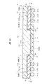
また、図27および図28に示されるように、放熱板4用のフレーム41を準備する(図22のステップS2)。図27には、フレーム41の平面図が示されているが、放熱板4の凸部12が形成されている側が示されている。図28は、図27のD1−D1線の断面図に対応する。なお、図27は、平面図であるが、フレーム41の形状が分かりやすいように、フレーム41にハッチングを付してある。また、図27のD1−D1線の位置は、上記図5〜図10のA1−A1線の位置および上記図13のB1−B1線の位置に対応しているため、図28は上記図16と同じ断面が示されているが、図28と上記図16とでは、上下が逆になっている。   Also, as shown in FIGS. 27 and 28, a frame 41 for the heat sink 4 is prepared (step S2 in FIG. 22). In FIG. 27, a plan view of the frame 41 is shown, but the side on which the convex portion 12 of the heat sink 4 is formed is shown. FIG. 28 corresponds to a cross-sectional view taken along line D1-D1 of FIG. FIG. 27 is a plan view, but the frame 41 is hatched so that the shape of the frame 41 can be easily understood. 27 corresponds to the position of the A1-A1 line in FIGS. 5 to 10 and the position of the B1-B1 line in FIG. 13, and FIG. Although the same cross section is shown, FIG. 28 and FIG. 16 are upside down.

フレーム41は、複数の放熱板4がフレーム枠(枠部)42に一体的に連結された構造を有している。すなわち、同方向に延在する2本のフレーム枠42の間に、複数の放熱板4が所定の間隔で配置され、各放熱板4の基材部11の四隅近傍が連結部43を介してフレーム枠42と連結されている。フレーム41は、例えば、銅板などを金型で加工することなどにより形成することができる。また、フレーム41において、隣り合う放熱板4の間に、フレーム枠42同士を連結する連結部44が、フレーム41の補強のために設けられている。不要であれば、連結部43は省略することもできる。フレーム41においては、放熱板4、フレーム枠42、連結部43および連結部44は、同じ材料により一体的に形成されている。   The frame 41 has a structure in which a plurality of heat radiating plates 4 are integrally connected to a frame frame (frame portion) 42. That is, between the two frame frames 42 extending in the same direction, a plurality of the heat radiating plates 4 are arranged at a predetermined interval, and the vicinity of the four corners of the base material portion 11 of each heat radiating plate 4 is connected via the connecting portion 43. The frame 42 is connected. The frame 41 can be formed, for example, by processing a copper plate or the like with a mold. Further, in the frame 41, a connecting portion 44 that connects the frame frames 42 is provided between the adjacent radiator plates 4 to reinforce the frame 41. If unnecessary, the connecting portion 43 can be omitted. In the frame 41, the heat radiating plate 4, the frame frame 42, the connecting portion 43, and the connecting portion 44 are integrally formed of the same material.

上述したように、各放熱板4は、主面11aと主面11aとは反対側の裏面11bとを有する基材部と、基材部11の主面11aにおける中央部に位置しかつ基材部11aから突出する凸部12と、基材部11の主面11aに形成されかつ凸部12よりも低い支持部13とを一体的に有しており、凸部12の主面12aには溝(凹部、窪み部)16が形成されている。   As described above, each heat radiating plate 4 is located at the center of the base surface 11a and the back surface 11b opposite to the main surface 11a, and at the center of the main surface 11a of the base 11 and The convex portion 12 protruding from the portion 11a and the support portion 13 formed on the main surface 11a of the base material portion 11 and lower than the convex portion 12 are integrally provided, and the main surface 12a of the convex portion 12 has Grooves (recesses and depressions) 16 are formed.

次に、ダイボンディング工程を行って、フレーム41の各放熱板4の凸部12の主面12a上に、半導体チップ5を接合材14を介して搭載して接合する(図22のステップS3)。ステップS3の半導体チップ5の接合工程(すなわちダイボンディング工程)は、次のようにして行うことができる。   Next, a die bonding process is performed, and the semiconductor chip 5 is mounted and bonded to the main surface 12a of the convex portion 12 of each heat sink 4 of the frame 41 via the bonding material 14 (step S3 in FIG. 22). . The bonding process (that is, the die bonding process) of the semiconductor chip 5 in step S3 can be performed as follows.

すなわち、図29(上記図27と同じ領域の平面図)および図30(上記図28に対応する断面図)に示されるように、フレーム41の各放熱板4の凸部12の主面12aが上方を向くように、フレーム41の下面側を上方に向けた状態にしてから、フレーム41の各放熱板4の凸部12の主面12a上に、半田14aを塗布(配置)する。それから、必要に応じてフレーム41の各放熱板4の凸部12の主面12a上の半田14aを攪拌してから、図31(上記図27および図29と同じ領域の平面図)および図32(上記図28および図30に対応する断面図)に示されるように、フレーム41の各放熱板4の凸部12の主面12a上に半導体チップ5を半田14aを介して搭載(配置)する。これらの工程、すなわち、フレーム41の各放熱板4の凸部12への半田14aの塗布工程、半田14aの攪拌工程および放熱板4の凸部12への半導体チップ5の搭載工程は、放熱板4を含むフレーム41全体を加熱しながら行い、放熱板4の凸部12への半導体チップ5の搭載工程後にフレーム41を室温程度まで冷却する。これにより、半導体チップ5の搭載時には溶融状態であった半田14aが固化し、固化した半田14aによって、半導体チップ5が放熱板4の凸部12(の主面12a)に接合されて固定される。この固化した半田14aが、上記接合材14となる。   That is, as shown in FIG. 29 (a plan view of the same region as FIG. 27) and FIG. 30 (a cross-sectional view corresponding to FIG. 28), the main surface 12a of the convex portion 12 of each radiator plate 4 of the frame 41 is Solder 14a is applied (arranged) on the main surface 12a of the convex portion 12 of each heat radiating plate 4 of the frame 41 after the lower surface side of the frame 41 faces upward so as to face upward. Then, if necessary, the solder 14a on the main surface 12a of the convex portion 12 of each heat sink 4 of the frame 41 is stirred, and then FIG. 31 (plan view of the same region as FIG. 27 and FIG. 29) and FIG. As shown in (a cross-sectional view corresponding to FIGS. 28 and 30), the semiconductor chip 5 is mounted (arranged) on the main surface 12a of the convex portion 12 of each heat sink 4 of the frame 41 via the solder 14a. . These steps, that is, the step of applying the solder 14a to the convex portion 12 of each heat sink 4 of the frame 41, the step of stirring the solder 14a, and the step of mounting the semiconductor chip 5 on the convex portion 12 of the heat sink 4 are as follows. 4 is performed while heating the entire frame 41 including 4, and the frame 41 is cooled to about room temperature after the step of mounting the semiconductor chip 5 on the convex portion 12 of the heat sink 4. As a result, the solder 14a in a molten state is solidified when the semiconductor chip 5 is mounted, and the semiconductor chip 5 is joined and fixed to the convex portion 12 (the main surface 12a) of the heat sink 4 by the solidified solder 14a. . The solidified solder 14 a becomes the bonding material 14.

半田14aは、高融点半田を用いることが好ましく、少なくとも、後でバンプランドLA上に形成する外部端子(ここでは半田ボール9)に用いる半田の融点よりも高い融点を有する半田を、半田14aとして用いることが好ましい。これにより、後述するステップS9の半田ボール9接続工程や、完成した半導体装置1の実装工程(上記実装基板21に半導体装置1を実装する工程)で、半田ボール9を溶融させても、半導体チップ5と放熱板4の凸部12とを接合する半田14a(すなわち半田14aからなる接合材14)が溶融するのを防止できる。これにより、半導体チップ5と放熱板4の凸部12との接合信頼性を向上させることができ、半導体チップ5から放熱板4への熱伝導性を向上して、半導体装置1の放熱性を向上させることができる。   The solder 14a is preferably a high melting point solder, and at least a solder having a melting point higher than that of the solder used for the external terminal (here, the solder ball 9) to be formed later on the bump land LA is used as the solder 14a. It is preferable to use it. As a result, even if the solder ball 9 is melted in the solder ball 9 connecting step of step S9 described later or the mounting step of the completed semiconductor device 1 (step of mounting the semiconductor device 1 on the mounting substrate 21), the semiconductor chip It is possible to prevent melting of the solder 14a (that is, the bonding material 14 made of the solder 14a) that joins 5 and the convex portion 12 of the heat radiating plate 4. Thereby, the joining reliability of the semiconductor chip 5 and the convex part 12 of the heat sink 4 can be improved, the thermal conductivity from the semiconductor chip 5 to the heat sink 4 is improved, and the heat dissipation of the semiconductor device 1 is improved. Can be improved.

また、ステップS3の半導体チップ5の接合工程では、各放熱板4の凸部12の主面12aにおいて、溝16が形成されている領域よりも中央側に半導体チップ5が搭載される。そして、各放熱板4の凸部12の主面12aに設けられている溝16には、半田14a(接合材14)が付着しないようにする。なお、溝16と半導体チップ5との間に、更に溝を設けることで、より確実に、各放熱板4の凸部12の主面12aの溝16が接合材14で埋まるのを防止することができる。   Further, in the bonding step of the semiconductor chip 5 in step S3, the semiconductor chip 5 is mounted on the center side of the main surface 12a of the convex portion 12 of each heat sink 4 with respect to the region where the groove 16 is formed. And it is made for the solder 14a (joining material 14) not to adhere to the groove | channel 16 provided in the main surface 12a of the convex part 12 of each heat sink 4. As shown in FIG. In addition, by providing a further groove between the groove 16 and the semiconductor chip 5, it is possible to more reliably prevent the groove 16 of the main surface 12 a of the convex portion 12 of each heat sink 4 from being filled with the bonding material 14. Can do.

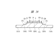
次に、半導体チップ5が搭載されている各放熱板4を、フレーム41のフレーム枠42から切断して分離する(図22のステップS4)。すなわち、放熱板4とフレーム枠42との連結部43を切断することで、半導体チップ5が搭載されている各放熱板4を、フレーム41のフレーム枠42から分離する。図33(平面図)および図34(上記図28、図30および図32に対応する断面図)に示されるように、半導体チップ5が搭載されている放熱板4が個片化される。   Next, each heat sink 4 on which the semiconductor chip 5 is mounted is cut and separated from the frame frame 42 of the frame 41 (step S4 in FIG. 22). That is, by cutting the connecting portion 43 between the heat radiating plate 4 and the frame frame 42, each heat radiating plate 4 on which the semiconductor chip 5 is mounted is separated from the frame frame 42 of the frame 41. As shown in FIG. 33 (plan view) and FIG. 34 (cross-sectional views corresponding to FIGS. 28, 30 and 32), the heat sink 4 on which the semiconductor chip 5 is mounted is separated.

また、本実施の形態では、ステップS3において、フレーム41に複数の放熱板4が連結された状態で、それら複数の放熱板4にの複数の半導体チップ5をそれぞれに接合してから、ステップS4で、半導体チップ5が搭載されている各放熱板4を個片化する場合について説明したが、他の形態として、ステップS3とステップS4との順番を入れ換えることもできる。ステップS3とステップS4との順番を入れ換える場合には、ステップS3のダイボンディング工程を行う前に、ステップS4を行って放熱板4をフレーム枠42から分離して個片化してから、個片化された各放熱板4の凸部12の主面12a上に、ステップS3として半導体チップ5を接合材14を介して接合すればよい。この場合のステップS3のダイボンディング工程の具体的な手法は、放熱板4が既に個片化されている以外は、上述した手法とほぼ同様に行うことができる。   In the present embodiment, in step S3, the plurality of heat sinks 4 are connected to the frame 41, and the plurality of semiconductor chips 5 are joined to the plurality of heat sinks 4, respectively. In the above description, the individual heat sinks 4 on which the semiconductor chips 5 are mounted are separated. However, as another form, the order of step S3 and step S4 can be interchanged. When the order of step S3 and step S4 is interchanged, before performing the die bonding process of step S3, step S4 is performed to separate the heat sink 4 from the frame frame 42 and separate into individual pieces. What is necessary is just to join the semiconductor chip 5 via the bonding | jointing material 14 as step S3 on the main surface 12a of the convex part 12 of each heat sink 4 performed. The specific method of the die bonding process in step S3 in this case can be performed in substantially the same manner as described above, except that the heat radiating plate 4 has already been separated.

次に、図35〜図37に示されるように、半導体チップ5が搭載されている放熱板4の凸部12を、配線基板31の各半導体装置領域32の貫通孔3内に配置(挿入)する(図22のステップS5)。それから、各放熱板4(の凸部12)を配線基板31(の各貫通孔3)にかしめることにより、各放熱板4を配線基板31に固定する(図22のステップS6)。図35〜図37は、ステップS5,S6が行われた段階を示す平面図(図35および図36)または断面図(図37)である。図35および図36には、上記図25と同じ領域(すなわち3つの半導体装置領域32)が示されているが、図35には、配線基板31の下面31b側が示され、図36には、配線基板31の上面31a側が示されている。また、図37には、上記図26に対応する断面図(すなわち図35および図36のC1−C1線の断面図)が示されている。なお、ステップS5,S6を行うと、上記C1−C1線の位置と上記D1−D1線の位置とは一致するものとなる。   Next, as shown in FIGS. 35 to 37, the protrusion 12 of the heat sink 4 on which the semiconductor chip 5 is mounted is disposed (inserted) in the through hole 3 of each semiconductor device region 32 of the wiring substrate 31. (Step S5 in FIG. 22). Then, each heat sink 4 is fixed to the wiring board 31 by caulking each heat sink 4 (projection 12 thereof) to the wiring board 31 (each through hole 3 thereof) (step S6 in FIG. 22). 35 to 37 are plan views (FIGS. 35 and 36) or cross-sectional views (FIG. 37) showing the stage where steps S5 and S6 are performed. 35 and FIG. 36 show the same region as in FIG. 25 (that is, three semiconductor device regions 32). FIG. 35 shows the lower surface 31b side of the wiring board 31, and FIG. The upper surface 31a side of the wiring board 31 is shown. FIG. 37 shows a cross-sectional view corresponding to FIG. 26 (that is, a cross-sectional view taken along line C1-C1 in FIGS. 35 and 36). In addition, if step S5, S6 is performed, the position of the said C1-C1 line will correspond with the position of the said D1-D1 line.

すなわち、ステップS5の放熱板4の配置工程では、放熱板4の基材部11の主面11aが配線基板31の上面31aに対向し、放熱板4の凸部12が配線基板31の貫通孔3内に位置し、放熱板4の支持部13(の支持面13a)が配線基板31の上面31aに接触するように、配線基板31の上面31a側に放熱板4を配置する。これにより、配線基板31の各貫通孔3に放熱板4の凸部12が挿入(配置)された状態となり、貫通孔3内に配置された凸部12の側面12bが貫通孔3の内壁に対向するが、この段階では、放熱板4は配線基板31にまだ固定されていない。そして、ステップS6では、放熱板4の凸部12の主面12aに設けられている溝16を押し広げる(例えば後述の治具46のような治具により溝16を押し広げる)ことにより、凸部12の側面12bの一部を貫通孔3の内壁と直接的に接触させることで、各放熱板4(の凸部12)を配線基板31(の各貫通孔3)にかしめて固定する。   That is, in the step of arranging the heat sink 4 in step S5, the main surface 11a of the base 11 of the heat sink 4 faces the upper surface 31a of the wiring board 31, and the convex portion 12 of the heat sink 4 is a through hole of the wiring board 31. 3, the heat sink 4 is arranged on the upper surface 31 a side of the wiring board 31 so that the support portion 13 (the support surface 13 a thereof) of the heat sink 4 is in contact with the upper surface 31 a of the wiring board 31. As a result, the convex portions 12 of the heat sink 4 are inserted (arranged) into the respective through holes 3 of the wiring board 31, and the side surfaces 12 b of the convex portions 12 disposed in the through holes 3 are formed on the inner walls of the through holes 3. Although facing each other, at this stage, the heat sink 4 is not yet fixed to the wiring board 31. In step S6, the groove 16 provided on the main surface 12a of the convex portion 12 of the heat radiating plate 4 is expanded (for example, the groove 16 is expanded by a jig such as a jig 46 described later). By directly contacting a part of the side surface 12 b of the portion 12 with the inner wall of the through hole 3, each heat radiating plate 4 (the convex portion 12) is caulked and fixed to the wiring board 31 (each through hole 3).

このステップS5,S6を行う前に、上記ステップS1で配線基板31を準備しておく必要がある。このため、上記ステップS1の配線基板31の準備工程は、ステップS2の前、ステップS2と同時、ステップS2の後でステップS3の前、ステップS3と同時、ステップS3の後でステップS4の前、ステップS4と同時、あるいはステップS4の後でステップS5の前に行うこともできる。   Before performing steps S5 and S6, it is necessary to prepare the wiring board 31 in step S1. For this reason, the preparation process of the wiring board 31 in step S1 is performed before step S2, simultaneously with step S2, after step S2, before step S3, simultaneously with step S3, after step S3, before step S4, It can be performed simultaneously with step S4 or after step S4 and before step S5.

ステップS5,S6の放熱板4の配置工程および固定(かしめ)工程については、後でより詳細に説明する。   The arrangement process and the fixing (caulking) process of the heat sink 4 in steps S5 and S6 will be described in detail later.

次に、図38および図39に示されるように、ワイヤボンディング工程を行って、半導体チップ5の各電極パッドPDと、これに対応する配線基板31に形成されたボンディングリードBLとを、導電性接続部材であるボンディングワイヤBWを介して電気的に接続する(図22のステップS7)。図38および図39は、それぞれステップS7のワイヤボンディング工程が行われた段階を示す平面図(図38)および断面図(図39)である。図38には、上記図25および図35と同じ領域(すなわち3つの半導体装置領域32)が示されており、配線基板31の下面31b側が示されている。また、図39には、上記図37に対応する断面図(すなわち上記C1−C1線に対応する位置での断面図)が示されている。   Next, as shown in FIGS. 38 and 39, a wire bonding step is performed to connect each electrode pad PD of the semiconductor chip 5 and the bonding lead BL formed on the wiring substrate 31 corresponding thereto to conductivity. Electrical connection is made via a bonding wire BW which is a connecting member (step S7 in FIG. 22). 38 and 39 are a plan view (FIG. 38) and a cross-sectional view (FIG. 39) showing the stage where the wire bonding process of step S7 is performed, respectively. FIG. 38 shows the same region as FIG. 25 and FIG. 35 (that is, three semiconductor device regions 32), and the lower surface 31b side of the wiring board 31 is shown. FIG. 39 shows a cross-sectional view corresponding to FIG. 37 (that is, a cross-sectional view at a position corresponding to the C1-C1 line).

すなわち、ステップS7のワイヤボンディング工程では、配線基板31の下面31bが上方を向いた状態で、配線基板31の下面31bの各半導体装置領域32の複数のボンディングリードBLと、その半導体装置領域32の貫通孔3内に配置された放熱板4の凸部12上に接合(搭載)された半導体チップ5の複数の電極パッドPDとを、複数のボンディングワイヤ(導電性接続部材)BWを介してそれぞれ電気的に接続する。   That is, in the wire bonding process of step S7, a plurality of bonding leads BL in each semiconductor device region 32 of the lower surface 31b of the wiring substrate 31 and the semiconductor device region 32 in a state where the lower surface 31b of the wiring substrate 31 faces upward. A plurality of electrode pads PD of the semiconductor chip 5 bonded (mounted) on the convex portion 12 of the heat sink 4 disposed in the through hole 3 are respectively connected via a plurality of bonding wires (conductive connection members) BW. Connect electrically.

本実施の形態とは異なり、ステップS6(放熱板4のかしめによる固定工程)を省略した場合には、ステップS7のワイヤボンディング工程や後述のステップS8のモールド工程で、放熱板4が配線基板31から外れてしまう虞がある。それに対して、本実施の形態では、ステップS6で放熱板4を配線基板31にかしめて固定することで、その後に行うステップS7のワイヤボンディング工程などで(すなわち後述のステップS8のモールド工程で封止部7c,8が形成されるまでに)、放熱板4が配線基板31から外れてしまうのを防止することができる。   Unlike this embodiment, when step S6 (fixing step by caulking of the heat sink 4) is omitted, the heat sink 4 is connected to the wiring board 31 in the wire bonding step of step S7 or the molding step of step S8 described later. There is a risk that it will come off. On the other hand, in the present embodiment, the heat sink 4 is caulked and fixed to the wiring board 31 in step S6, so that it is sealed in a wire bonding process in step S7 performed later (that is, in a molding process in step S8 described later). It is possible to prevent the heat radiating plate 4 from being detached from the wiring board 31 until the stop portions 7c and 8 are formed.

ステップS7のワイヤボンディング工程の後、図40〜図42に示されるように、モールド工程(例えばトランスファモールド工程)による樹脂封止を行って封止部7c,8を形成する(図22のステップS8)。封止部8により、配線基板31の下面31b側において、各半導体装置領域32の半導体チップ5および複数のボンディングワイヤBWが封止(樹脂封止)される。このため、ステップS8のモールド工程は、各半導体装置領域32の半導体チップ5および複数のボンディングワイヤ(導電性接続部材)BWを樹脂封止する工程とみなすこともできる。   After the wire bonding process in step S7, as shown in FIGS. 40 to 42, resin sealing is performed by a molding process (for example, transfer molding process) to form the sealing portions 7c and 8 (step S8 in FIG. 22). ). By the sealing portion 8, the semiconductor chip 5 and the plurality of bonding wires BW in each semiconductor device region 32 are sealed (resin sealed) on the lower surface 31 b side of the wiring substrate 31. For this reason, the molding process of step S8 can also be regarded as a process of resin-sealing the semiconductor chip 5 and the plurality of bonding wires (conductive connection members) BW in each semiconductor device region 32.

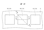
図40〜図42は、ステップS8のモールド工程によって封止部7c,8が形成された段階を示す平面図(図40および図41)または断面図(図42)である。図40および図41には、上記図36および図35と同じ領域(すなわち3つの半導体装置領域32)が示されているが、図40には、配線基板31の上面31a側(すなわち封止部7c側)が示され、図41には、配線基板31の下面31b側が示されている。また、図42には、上記図37および図39に対応する断面図(すなわち図40および図41のC1−C1線の断面図)が示されているが、上記図37および図39は、配線基板31の下面31b側が上方を向いた向きで示されていたのに対して、図42の断面図は、配線基板31の上面31a側が上方を向いた向きで示されている。   40 to 42 are plan views (FIGS. 40 and 41) or cross-sectional views (FIG. 42) showing a stage where the sealing portions 7c and 8 are formed by the molding process of step S8. 40 and 41 show the same region (that is, three semiconductor device regions 32) as in FIGS. 36 and 35, but FIG. 40 shows the upper surface 31a side of the wiring substrate 31 (that is, the sealing portion). 7c side) and FIG. 41 shows the lower surface 31b side of the wiring board 31. 42 shows a cross-sectional view corresponding to FIGS. 37 and 39 (that is, a cross-sectional view taken along line C1-C1 in FIGS. 40 and 41). FIG. 37 and FIG. Whereas the lower surface 31b side of the substrate 31 is shown facing upward, the cross-sectional view of FIG. 42 shows the upper surface 31a side of the wiring substrate 31 facing upward.

本実施の形態では、ステップS8のモールド工程において、配線基板31の上面31a側の封止部7cと下面31b側の封止部8とを一括して(一度に)形成している。封止部7cは、配線基板31の上面31aの複数の半導体装置領域32全体を覆うように形成される。一方、封止部8は、配線基板31の下面31bの複数の半導体装置領域32のそれぞれにおいて、半導体チップ5およびボンディングワイヤBWを覆うように形成され、個々の半導体装置領域32に対して形成された封止部8同士は、互いに分離されている。   In the present embodiment, in the molding step of step S8, the sealing portion 7c on the upper surface 31a side and the sealing portion 8 on the lower surface 31b side of the wiring substrate 31 are formed all at once (at a time). The sealing portion 7 c is formed so as to cover the entire plurality of semiconductor device regions 32 on the upper surface 31 a of the wiring substrate 31. On the other hand, the sealing portion 8 is formed so as to cover the semiconductor chip 5 and the bonding wire BW in each of the plurality of semiconductor device regions 32 on the lower surface 31 b of the wiring substrate 31, and is formed for each semiconductor device region 32. The sealed portions 8 are separated from each other.

また、本実施の形態では、ステップS8のモールド工程において、配線基板31の上面31a側(具体的には後述のキャビティCAV1)に供給した樹脂材料MRを、上記隙間部15を通じて配線基板31の下面31b側(具体的には後述のキャビティCAV2)にも供給し、この樹脂材料MRによって、配線基板31の上面31a側の封止部7cと配線基板31の下面31b側の封止部8とを形成している。このステップS8のモールド工程については、後でより詳細に説明する。   In the present embodiment, the resin material MR supplied to the upper surface 31a side (specifically, a cavity CAV1 described later) of the wiring substrate 31 in the molding step of step S8 is passed through the gap portion 15 to the lower surface of the wiring substrate 31. The resin material MR also supplies the sealing portion 7c on the upper surface 31a side of the wiring substrate 31 and the sealing portion 8 on the lower surface 31b side of the wiring substrate 31 with the resin material MR. Forming. The molding process in step S8 will be described in detail later.

上記ステップS6で配線基板31に放熱板4の凸部12をかしめて固定した後、ステップS8のモールド工程を行うまでは、かしめによって配線基板31に放熱板4が固定される。これにより、封止部7c,8を形成する前に、放熱板4が配線基板31の貫通孔3から外れてしまうのを防止することができる。封止部7c,8を形成すると、放熱板4と配線基板31とは封止部7c,8で強固に結合されるので、封止部7c,8を形成した後は、負荷や荷重などがかかったとしても、放熱板4が配線基板31の貫通孔3から外れてしまうのを的確に防止することができる。   The caulking plate 4 is fixed to the wiring board 31 by caulking after the protrusion 12 of the heat sink 4 is caulked and fixed to the wiring board 31 in step S6 until the molding step of step S8 is performed. Thereby, it can prevent that the heat sink 4 remove | deviates from the through-hole 3 of the wiring board 31 before forming the sealing parts 7c and 8. FIG. When the sealing portions 7c and 8 are formed, the heat radiating plate 4 and the wiring board 31 are firmly coupled by the sealing portions 7c and 8. Therefore, after the sealing portions 7c and 8 are formed, a load or a load is applied. Even if it takes, it can prevent exactly that the heat sink 4 remove | deviates from the through-hole 3 of the wiring board 31. FIG.

次に、図43に示されるように、配線基板31の下面31bの複数のバンプランドLAに複数の半田ボール9をそれぞれ接続(接合)する(図22のステップS9)。図43は、ステップS9の半田ボール9の接続工程を行った段階を示す断面図であり、上記図37、図39および図42に対応する断面図(すなわち上記C1−C1線に対応する位置での断面図)が示されている。但し、図43の断面図は、上記図42と同様、配線基板31の上面31a側が上方を向いた向きで示されている。   Next, as shown in FIG. 43, a plurality of solder balls 9 are respectively connected (joined) to a plurality of bump lands LA on the lower surface 31b of the wiring board 31 (step S9 in FIG. 22). FIG. 43 is a cross-sectional view showing the stage where the solder ball 9 connecting step of step S9 is performed, and is a cross-sectional view corresponding to FIGS. 37, 39 and 42 (that is, at a position corresponding to the C1-C1 line). Is a cross-sectional view). However, the cross-sectional view of FIG. 43 is shown with the upper surface 31a side of the wiring board 31 facing upward as in FIG.

ステップS9の半田ボール9の接続工程においては、例えば、配線基板31の下面31bを上方に向け、配線基板31の下面31bの複数のバンプランドLA上に複数の半田ボール9を配置してフラックスなどで仮固定し、半田リフロー処理(リフロー処理、熱処理)を行って半田を溶融、再固化することで、半田ボール9と配線基板31の下面31bのバンプランドLAとを接合して電気的に接続することができる。その後、必要に応じて洗浄工程を行い、半田ボール9の表面に付着したフラックスなどを取り除くこともできる。このようにして、ステップS9おいて、半導体装置1の外部端子としての半田ボール9が配線基板31の下面31bのバンプランドLA上に形成される。従って、ステップS9の半田ボール9の接続工程は、配線基板31の下面31bの複数のバンプランドLA上に複数の外部端子をそれぞれ形成する工程(すなわち外部端子形成工程)とみなすこともできる。   In the connecting step of the solder balls 9 in step S9, for example, a plurality of solder balls 9 are arranged on the plurality of bump lands LA on the lower surface 31b of the wiring substrate 31 with the lower surface 31b of the wiring substrate 31 facing upward, and flux or the like. And solder reflow treatment (reflow treatment, heat treatment) to melt and resolidify the solder, thereby joining and electrically connecting the solder balls 9 and the bump lands LA on the lower surface 31b of the wiring board 31. can do. Thereafter, if necessary, a cleaning process can be performed to remove flux and the like adhering to the surface of the solder ball 9. In this manner, in step S9, the solder balls 9 as the external terminals of the semiconductor device 1 are formed on the bump lands LA on the lower surface 31b of the wiring board 31. Therefore, the connecting process of the solder balls 9 in step S9 can be regarded as a process of forming a plurality of external terminals on the plurality of bump lands LA on the lower surface 31b of the wiring board 31 (that is, an external terminal forming process).

配線基板31の下面31bに接合された半田ボール9は、バンプ電極(半田バンプ)とみなすことができる。なお、本実施の形態では、半導体装置1の外部端子として半田ボール9をバンプランドLAに接合する場合について説明したが、これに限定されるものではない。例えば、半田ボール9の代わりに印刷法などによりバンプランドLA上に半田を供給して、半導体装置1の外部端子としてのバンプ電極(半田バンプ)をバンプランドLA上に形成することもできる。また、半導体装置1の外部端子(ここでは半田ボール9)の材質には、鉛含有半田や鉛を含有しない鉛フリー半田のいずれを用いることもできるが、含有しない鉛フリー半田を用いればより好ましい。   The solder ball 9 bonded to the lower surface 31b of the wiring board 31 can be regarded as a bump electrode (solder bump). In the present embodiment, the case where the solder ball 9 is bonded to the bump land LA as the external terminal of the semiconductor device 1 has been described. However, the present invention is not limited to this. For example, solder may be supplied onto the bump lands LA by a printing method or the like instead of the solder balls 9 to form bump electrodes (solder bumps) as external terminals of the semiconductor device 1 on the bump lands LA. Further, as the material of the external terminal (here, the solder ball 9) of the semiconductor device 1, either lead-containing solder or lead-free solder not containing lead can be used, but it is more preferable to use lead-free solder that does not contain lead. .

次に、配線基板31とその上面31a上に形成された封止部7cとを各半導体装置領域32に切断(ダイシング)して分離(分割)する(図22のステップS10)。図44および図45は、ステップS10の切断工程を行う直前の状態を示す平面図(全体平面図)であり、それぞれ上記図23および図24と同じ領域、すなわち配線基板31全体が示されており、図44には、配線基板31の上面31a側が示され、図45には、配線基板31の下面31b側が示されている。また、図44および図45は、平面図であるが、図面を見やすくするために封止部7c,8にハッチングを付し、また、ステップS10で切断する際のダイシングラインDLを二点鎖線で示してある。   Next, the wiring substrate 31 and the sealing portion 7c formed on the upper surface 31a are cut (diced) into the semiconductor device regions 32 and separated (divided) (step S10 in FIG. 22). 44 and 45 are plan views (overall plan views) showing a state immediately before the cutting process in step S10, and the same region as that in FIGS. 23 and 24, that is, the entire wiring board 31 is shown. 44 shows the upper surface 31 a side of the wiring board 31, and FIG. 45 shows the lower surface 31 b side of the wiring board 31. FIG. 44 and FIG. 45 are plan views. In order to make the drawings easy to see, the sealing portions 7c and 8 are hatched, and the dicing line DL at the time of cutting in step S10 is a two-dot chain line. It is shown.

ステップS10の切断工程では、図44および図45に示されるダイシングライン(切断線、切断位置)DLに沿って、配線基板31を、その上面31a上の封止部7cとともに切断する。図44および図45と上記図23および図24とを比べると分かるように、上記半導体装置領域32の外周位置に沿って、ダイシングラインDLが延在している。すなわち、ステップS10の切断工程では、配線基板31とその上面31a上の封止部7cとが、各半導体装置領域32に分割されるのである。また、封止部8は、各半導体装置領域32の境界(すなわちダイシングラインDL)上には形成されていないので、ステップS10の切断工程では、封止部8は切断されない。   In the cutting step of Step S10, the wiring board 31 is cut along with the sealing portion 7c on the upper surface 31a along the dicing line (cutting line, cutting position) DL shown in FIGS. As can be seen from a comparison between FIGS. 44 and 45 and FIGS. 23 and 24, the dicing line DL extends along the outer peripheral position of the semiconductor device region 32. That is, in the cutting process of step S10, the wiring substrate 31 and the sealing portion 7c on the upper surface 31a are divided into the semiconductor device regions 32. Moreover, since the sealing part 8 is not formed on the boundary (namely, dicing line DL) of each semiconductor device area | region 32, the sealing part 8 is not cut | disconnected by the cutting process of step S10.

このように、ステップS10で切断・個片化を行うことで、図46に示されるような半導体装置1(すなわち上記図1〜図10に示される半導体装置1)を製造することができる。なお、図46は、上記図1と同じ断面図である。各半導体装置領域32に切断され分離(分割)された配線基板31が配線基板2に対応し、各半導体装置領域32に切断され分離(分割)された封止部7cが封止部7に対応する。また、配線基板31の上面31aが配線基板2の上面2aとなり、配線基板31の下面31bが配線基板2の下面2bとなる。   As described above, by cutting and separating in step S10, the semiconductor device 1 as shown in FIG. 46 (that is, the semiconductor device 1 shown in FIGS. 1 to 10) can be manufactured. 46 is the same cross-sectional view as FIG. The wiring substrate 31 cut and separated (divided) into each semiconductor device region 32 corresponds to the wiring substrate 2, and the sealing portion 7 c cut and separated (divided) into each semiconductor device region 32 corresponds to the sealing portion 7. To do. Further, the upper surface 31 a of the wiring substrate 31 becomes the upper surface 2 a of the wiring substrate 2, and the lower surface 31 b of the wiring substrate 31 becomes the lower surface 2 b of the wiring substrate 2.

<配線基板への放熱板の固定について>
上記ステップS5,S6の放熱板4の配置工程および固定(かしめ)工程について、より詳細に説明する。
<Fixing the heat sink to the wiring board>
The arrangement process and the fixing (caulking) process of the heat sink 4 in steps S5 and S6 will be described in more detail.

ステップS5,S6の放熱板4の配置工程および固定(かしめ)工程の具体的な手法を、図47〜図55を参照して説明する。図47〜図55は、ステップS5,S6の放熱板4の配置工程および固定(かしめ)工程の説明図であり、図47、図48および図50、図51、図53および図55には、上記図37に対応する断面図(すなわち上記C1−C1線およびD1−D1線に対応する位置での断面図)が示されている。また、図49は、図48における円で囲まれた領域RG3,RG4の部分拡大図に対応し、図52は、図51における円で囲まれた領域RG3,RG4の部分拡大図に対応し、図54は、図53における円で囲まれた領域RG3,RG4の部分拡大図に対応する。   The specific method of the arrangement | positioning process and fixing (caulking) process of the heat sink 4 of step S5, S6 is demonstrated with reference to FIGS. 47 to 55 are explanatory diagrams of the disposing process and the fixing (caulking) process of the heat sink 4 in steps S5 and S6. FIG. 47, FIG. 48 and FIG. 50, FIG. 51, FIG. A cross-sectional view corresponding to FIG. 37 (that is, a cross-sectional view at a position corresponding to the C1-C1 line and the D1-D1 line) is shown. 49 corresponds to a partially enlarged view of regions RG3 and RG4 surrounded by a circle in FIG. 48, and FIG. 52 corresponds to a partially enlarged view of regions RG3 and RG4 surrounded by a circle in FIG. 54 corresponds to a partially enlarged view of regions RG3 and RG4 surrounded by a circle in FIG.

まず、配線基板31を構成する半導体装置領域32の数に対応する数の放熱板4を、凸部12の主面12aが上方を向くように並べて配置する。この際、複数の放熱板4が、配線基板31における複数の半導体装置領域32の配列に対応して配列するようにする。例えば、これら複数の放熱板4を、図47に示されるように、トレイまたはキャリア45などに配置する。そして、このトレイまたはキャリア45について、複数の放熱板4の各凸部12を配線基板31の各貫通孔3に一括して挿入できるように各放熱板4を位置決めして配置可能な構成しておけばよい。複数の放熱板4が配置されたトレイまたはキャリア45は、図示しないステージ(台、作業台)などの上に載置(配置)されている。なお、図47および図48などには、1つの半導体装置領域32に対応する領域が示されているが、実際には、上述のように、複数の放熱板4がトレイまたはキャリア45に配置されている。   First, the number of heat radiation plates 4 corresponding to the number of semiconductor device regions 32 constituting the wiring board 31 are arranged side by side so that the main surface 12a of the convex portion 12 faces upward. At this time, the plurality of heat sinks 4 are arranged corresponding to the arrangement of the plurality of semiconductor device regions 32 in the wiring substrate 31. For example, the plurality of heat radiating plates 4 are arranged on a tray or a carrier 45 as shown in FIG. And about this tray or the carrier 45, each heat sink 4 is positioned and arrange | positioned so that each convex part 12 of the several heat sink 4 can be collectively inserted in each through-hole 3 of the wiring board 31. Just keep it. The tray or carrier 45 on which the plurality of heat sinks 4 are arranged is placed (arranged) on a stage (table, work table) or the like (not shown). 47 and 48 show an area corresponding to one semiconductor device area 32. Actually, as described above, a plurality of heat radiation plates 4 are arranged on the tray or carrier 45. ing.

それから、複数の放熱板4の上方に配線基板31を、配線基板31の上面31aが放熱板4の凸部12側を向くように配置してから、配線基板31を複数の放熱板4に近づくように(すなわち図47の矢印で示される方向に)移動(下降)させ、図48に示されるように、配線基板31に設けられた複数の半導体装置領域32の各貫通孔3に複数の放熱板4の各凸部12をそれぞれ挿入させる(差し込む)。   Then, after arranging the wiring board 31 above the plurality of heat sinks 4 so that the upper surface 31a of the wiring board 31 faces the convex portion 12 side of the heat sink 4, the wiring board 31 approaches the plurality of heat sinks 4. (That is, in the direction indicated by the arrow in FIG. 47), and a plurality of heat dissipations are made in the respective through holes 3 of the plurality of semiconductor device regions 32 provided in the wiring board 31 as shown in FIG. Each convex portion 12 of the plate 4 is inserted (inserted).

この際、図47に示されるように、複数の放熱板4を固定(例えばトレイまたはキャリア45に固定)した状態で、配線基板31を移動させて、配線基板31の各貫通孔3に各放熱板4の凸部12をそれぞれ挿入させることが、より好ましいが、他の形態として、配線基板31を固定した状態で放熱板4を移動させて、配線基板31の各貫通孔3に各放熱板4の凸部12をそれぞれ挿入させることもできる。すなわち、ステップS5では、配線基板31と複数の放熱板4との相対的な位置を移動させることで、配線基板31の各貫通孔3に各放熱板4の凸部12をそれぞれ挿入させる。いずれにしても、ステップS5では、半導体チップ5が搭載されている放熱板4の凸部12が、配線基板31の上面31a側(配線基板2の上面2aに対応する側)から、配線基板31の貫通孔3に挿入される。   At this time, as shown in FIG. 47, the wiring board 31 is moved in a state where the plurality of heat radiating plates 4 are fixed (for example, fixed to the tray or the carrier 45), and each heat dissipation is made to each through hole 3 of the wiring board 31. It is more preferable to insert the convex portions 12 of the plate 4, but as another form, the heat radiating plate 4 is moved in a state where the wiring substrate 31 is fixed, and each heat radiating plate is inserted into each through hole 3 of the wiring substrate 31. Each of the four convex portions 12 can be inserted. That is, in step S <b> 5, the protrusion 12 of each heat sink 4 is inserted into each through hole 3 of the wiring board 31 by moving the relative positions of the wiring board 31 and the plurality of heat sinks 4. In any case, in step S5, the convex portion 12 of the heat sink 4 on which the semiconductor chip 5 is mounted is from the upper surface 31a side of the wiring substrate 31 (the side corresponding to the upper surface 2a of the wiring substrate 2). Is inserted into the through hole 3.

放熱板4は、上述のように、基材部11と凸部12と支持部13とからなり、ステップS5では、この凸部12が配線基板31の貫通孔3内に配置(挿入、収容)されるとともに、基材部11は配線基板31の上面31a側に位置し、支持部13の支持面13aが配線基板31の上面31aに接した状態となる。   As described above, the heat radiating plate 4 includes the base portion 11, the convex portion 12, and the support portion 13. In step S 5, the convex portion 12 is disposed (inserted and accommodated) in the through hole 3 of the wiring substrate 31. At the same time, the base material portion 11 is located on the upper surface 31 a side of the wiring substrate 31, and the support surface 13 a of the support portion 13 is in contact with the upper surface 31 a of the wiring substrate 31.

図47〜図49からも分かるように、配線基板31の貫通孔3の内壁は、配線基板31の上面31aおよび下面31bに対して略垂直であり、放熱板4の凸部12の側面12bは、放熱板3の凸部12の主面12a、基材部11の主面11aおよび支持部13の支持面13aに対して略垂直である。そして、放熱板4の凸部12の断面形状(放熱板4の基材部12の主面12aや支持部13の支持面13aに略平行な断面での形状)を、配線基板31における貫通孔3の断面形状(配線基板31の上面31aおよび下面31bに略平行な断面での形状)と比べて同程度か若干小さくするが、若干小さい方が好ましい。放熱板4の凸部12の断面形状を、配線基板31における貫通孔3の断面形状よりも若干小さくしておくことで、ステップS5において放熱板4の凸部12を配線基板31の貫通孔3に挿入しやすくなる。   47 to 49, the inner wall of the through hole 3 of the wiring board 31 is substantially perpendicular to the upper surface 31a and the lower surface 31b of the wiring board 31, and the side surface 12b of the convex portion 12 of the heat sink 4 is The main surface 12 a of the convex portion 12 of the heat radiating plate 3, the main surface 11 a of the base material portion 11, and the support surface 13 a of the support portion 13 are substantially perpendicular. And the cross-sectional shape of the convex part 12 of the heat sink 4 (the shape in a cross section substantially parallel to the main surface 12a of the base 12 and the support surface 13a of the support 13 of the heat sink 4) 3 is substantially the same as or slightly smaller than the cross-sectional shape 3 (the shape of the cross-section substantially parallel to the upper surface 31a and the lower surface 31b of the wiring substrate 31), but is slightly smaller. By making the cross-sectional shape of the convex portion 12 of the heat sink 4 slightly smaller than the cross-sectional shape of the through hole 3 in the wiring substrate 31, the convex portion 12 of the heat sink 4 is made to pass through the through hole 3 of the wiring substrate 31 in step S <b> 5. Easy to insert into.

このようにして上記ステップS5を行うことで、配線基板31の各貫通孔3に放熱板4の凸部12が挿入(配置)された状態となるが、この段階では、放熱板4は配線基板31にまだ固定されていない。そこで、ステップS6で、各放熱板4の凸部12の主面12aに設けられている溝16を押し広げることにより、各放熱板4(の凸部12)を配線基板31(の各貫通孔3)に、かしめて固定する。これは、治具(かしめ用治具)46のような治具により、放熱板4の凸部12の主面12aの溝16を押し広げることで実現できる。   By performing step S5 as described above, the projection 12 of the heat sink 4 is inserted (arranged) into each through hole 3 of the wiring board 31. At this stage, the heat sink 4 is connected to the wiring board. 31 is not yet fixed. Therefore, in step S6, the heat sinks 4 (projections 12 thereof) are connected to the wiring boards 31 (each through-holes) by expanding the grooves 16 provided in the main surface 12a of the projections 12 of the heat sinks 4. 3) Fix by caulking. This can be realized by expanding the groove 16 of the main surface 12a of the convex portion 12 of the heat radiating plate 4 with a jig such as a jig (caulking jig) 46.

具体的に説明すると、放熱板4の凸部12の主面12aの上方に配置されたかしめ用の冶具46を、図50の矢印で示される方向(すなわち放熱板4の凸部12の主面12aに略垂直でかつこの主面12aに近づく方向)に、溝16に向かって移動(降下)させることで、図51に示されるように、治具46の先端部47で溝16を叩く。換言すれば、治具46の先端部47が溝16に重なるように、治具46の先端部47を溝16に押し付ける(押し込む)。   Specifically, the caulking jig 46 disposed above the main surface 12a of the convex portion 12 of the heat radiating plate 4 is moved in the direction indicated by the arrow in FIG. 50 (that is, the main surface of the convex portion 12 of the heat radiating plate 4). By moving (lowering) toward the groove 16 in a direction substantially perpendicular to 12a and approaching the main surface 12a, the groove 16 is hit by the tip 47 of the jig 46 as shown in FIG. In other words, the tip portion 47 of the jig 46 is pressed (pushed) into the groove 16 so that the tip portion 47 of the jig 46 overlaps the groove 16.

この際、治具46の先端部47は、溝16の延在方向に垂直な断面(図50〜図52の断面図)で見ると、先細りのテーパ形状を有している。そして、治具46の先端部47における最先端は、溝16の幅(溝16の延在方向に垂直な方向の幅であって、凸部12の主面12a側の開口幅)W1とほぼ同じか若干小さい。なお、幅W1は図49に図示されている。しかしながら、治具46の先端部47がテーパ形状を有しているために、図51および図52に示されるように、治具46の先端部47の最先端が溝16の底部に到達したときには、放熱板4の凸部12の主面12aの位置では、治具46の先端部47は、溝16の幅W1よりも大きな寸法を有することになる。   At this time, the tip portion 47 of the jig 46 has a tapered shape when viewed in a cross section perpendicular to the extending direction of the groove 16 (cross sectional views of FIGS. 50 to 52). The leading edge of the tip portion 47 of the jig 46 is substantially the same as the width of the groove 16 (the width in the direction perpendicular to the extending direction of the groove 16 and the opening width on the main surface 12a side of the convex portion 12) W1. Same or slightly smaller. The width W1 is illustrated in FIG. However, since the tip portion 47 of the jig 46 has a taper shape, as shown in FIGS. 51 and 52, when the tip end of the tip portion 47 of the jig 46 reaches the bottom of the groove 16. The tip portion 47 of the jig 46 has a size larger than the width W1 of the groove 16 at the position of the main surface 12a of the convex portion 12 of the heat sink 4.

このため、上述のように治具46の先端部47で溝16を叩く(治具46の先端部47を溝16に押し付ける)と、図52に示されるように、溝16が冶具46の先端部47で押し広げられる(すなわち上記幅W1が溝16の上部で広げられる)。そして、押し広げられた体積分だけ、水平方向(凸部12の主面12aに平行な方向)に凸部12の一部が広がり、放熱板4の凸部12の側面12bの一部(側面12bの上部)が、配線基板31の貫通孔3の内壁面に直接的に接触して密着する。この反作用により、配線基板31の貫通孔3の内壁が凸部12の側面12bの一部に密着して押すような力を作用させ、それによって、配線基板31の貫通孔3の内壁によって放熱板4の凸部12の側面12bが締め付けられる。これにより、放熱板4(の凸部12)と配線基板31とを、かしめることができ、放熱板4を配線基板31に固定することができる。   For this reason, when the groove 16 is hit with the tip 47 of the jig 46 as described above (the tip 47 of the jig 46 is pressed against the groove 16), the groove 16 becomes the tip of the jig 46 as shown in FIG. It is pushed and widened at the portion 47 (that is, the width W1 is widened at the upper portion of the groove 16). Then, a part of the convex part 12 spreads in the horizontal direction (a direction parallel to the main surface 12a of the convex part 12) by the expanded volume, and a part of the side surface 12b of the convex part 12 of the heat sink 4 (side surface). 12b) directly contacts and adheres to the inner wall surface of the through hole 3 of the wiring board 31. Due to this reaction, a force is applied such that the inner wall of the through hole 3 of the wiring board 31 is in close contact with and pressed against a part of the side surface 12 b of the convex portion 12. The side surface 12b of the four convex portions 12 is tightened. Thereby, the heat sink 4 (the convex part 12) and the wiring board 31 can be crimped, and the heat sink 4 can be fixed to the wiring board 31.

治具46の先端部47を溝16に押し付けることで、放熱板4の凸部12の主面12aの溝16を押し広げてから、図53に示されるように、治具46を上昇させて放熱板4の凸部12から離れさせる。これにより、治具46の先端部47は溝16から離れるが、図54に示されるように、放熱板4の凸部12の側面12bの一部(側面12bの上部)が、配線基板31の貫通孔3の内壁面に直接的に接触して密着した状態は維持される。すなわち、放熱板4(の凸部12)が配線基板31にかしめられて固定された状態は維持される。   By pressing the tip portion 47 of the jig 46 against the groove 16, the groove 16 on the main surface 12 a of the convex portion 12 of the heat radiating plate 4 is expanded and then the jig 46 is raised as shown in FIG. 53. It is made to separate from the convex part 12 of the heat sink 4. FIG. Thereby, the tip portion 47 of the jig 46 is separated from the groove 16, but as shown in FIG. 54, a part of the side surface 12 b (upper side surface 12 b) of the convex portion 12 of the heat radiating plate 4 is formed on the wiring substrate 31. The state of being in direct contact with the inner wall surface of the through hole 3 is maintained. That is, the state where the heat radiating plate 4 (the convex portion 12) is caulked and fixed to the wiring board 31 is maintained.

なお、放熱板4の凸部12の主面12aの溝16を押し広げて放熱板4(の凸部12)を配線基板31にかしめる(固定する)ことができるのであれば、治具46の形状などについては種々変更可能である。   If the groove 16 on the main surface 12a of the convex portion 12 of the heat sink 4 can be expanded and the heat sink 4 (the convex portion 12) can be caulked (fixed) to the wiring board 31, a jig 46 can be used. Various changes can be made to the shape and the like.

このようにして、上記ステップS6を行って放熱板4(の凸部12)を配線基板31にかしめて固定した後、図55に示されるように、配線基板3に固定された(かしめられた)複数の放熱板4を、トレイまたはキャリア45から離脱させる(取り外す)。これは、トレイまたはキャリア45について、トレイまたはキャリア45から放熱板4を容易に離脱可能(取り外し可能)な構成としておけばよい。その後、複数の放熱板4が固定された(かしめられた)配線基板31は、次の工程(ここでは上記ステップS7のワイヤボンディング工程)に送られる。   Thus, after performing step S6 and caulking and fixing the heat radiating plate 4 (projection 12 thereof) to the wiring board 31, it was fixed (caulked) to the wiring board 3 as shown in FIG. ) Remove (remove) the plurality of heat sinks 4 from the tray or carrier 45. For this purpose, the tray or carrier 45 may be configured such that the heat radiating plate 4 can be easily detached (removable) from the tray or carrier 45. Thereafter, the wiring board 31 to which the plurality of heat sinks 4 are fixed (crimped) is sent to the next step (here, the wire bonding step in step S7).

本実施の形態では、ステップS6で放熱板4を配線基板31にかしめて固定することで、その後に封止部7c,8が形成されるまでに、放熱板4が配線基板31から外れてしまうのを防止することができる。   In this embodiment, the heat sink 4 is detached from the wiring board 31 until the sealing portions 7c and 8 are formed after the heat sink 4 is caulked and fixed to the wiring board 31 in step S6. Can be prevented.

放熱板4の凸部12の主面12aに設けた溝16は、この溝16を治具46で押し広げることにより、放熱板4(の凸部12)を配線基板31(の貫通孔3)にかしめて固定するために用いるものである。このため、上記図8〜図10および図14に示されるように、放熱板4の凸部12の主面12aの周辺部に溝16を設けることが好ましい。また、放熱板4の凸部12の主面12aにおいて、少なくとも対向する二辺のそれぞれに沿って溝16を設けることが好ましく、放熱板4の凸部12の主面12aにおいて、四辺のそれぞれに沿って溝16を設ければ、更に好ましい。このようにすることで、溝16を治具46で押し広げた際に、凸部12の側面12bの一部を配線基板31の貫通孔3の内壁と直接的に接触させて、放熱板4を配線基板に的確にかしめて固定することができるようになる。すなわち、放熱板4の支持部13の支持面13aと、放熱板4の凸部12の側面12bとで、配線基板31の一部を挟み込むことができる。   The groove 16 provided on the main surface 12a of the convex portion 12 of the heat sink 4 is formed by pushing the groove 16 with a jig 46 so that the heat sink 4 (the convex portion 12) is connected to the wiring board 31 (the through hole 3). It is used for caulking and fixing. For this reason, as shown in FIGS. 8 to 10 and 14, it is preferable to provide the groove 16 in the peripheral portion of the main surface 12 a of the convex portion 12 of the heat sink 4. Moreover, it is preferable to provide the groove 16 along each of at least two opposite sides in the main surface 12a of the convex portion 12 of the heat sink 4, and in each of the four sides in the main surface 12a of the convex portion 12 of the heat sink 4 It is more preferable to provide the groove 16 along the groove. In this way, when the groove 16 is pushed out by the jig 46, a part of the side surface 12 b of the convex portion 12 is brought into direct contact with the inner wall of the through hole 3 of the wiring substrate 31, and the heat radiating plate 4. Can be accurately caulked and fixed to the wiring board. That is, a part of the wiring board 31 can be sandwiched between the support surface 13 a of the support portion 13 of the heat sink 4 and the side surface 12 b of the convex portion 12 of the heat sink 4.

また、本実施の形態とは異なり、放熱板4の凸部12の主面12aにおいて、半導体チップ5が搭載される領域(搭載された半導体チップ5と平面的に重なる領域)にのみ溝16を形成し、半導体チップ5が搭載される領域以外に溝16を形成しなかった場合には、ステップS6で、半導体チップ5が邪魔になって凸部12の主面12aの溝16を治具46で押し広げられなくなってしまう。   Further, unlike the present embodiment, the groove 16 is formed only in a region where the semiconductor chip 5 is mounted (a region overlapping the mounted semiconductor chip 5 in a plane) on the main surface 12a of the convex portion 12 of the heat sink 4. In the case where the groove 16 is not formed except for the region where the semiconductor chip 5 is mounted, the groove 16 on the main surface 12a of the convex portion 12 is blocked by the jig 46 in step S6. It becomes impossible to spread with.

それに対して、本実施の形態では、放熱板4の凸部12の主面12aにおいて、かしめ用の溝16は、半導体チップ5が搭載される領域(搭載された半導体チップ5と平面的に重なる領域)以外の領域に形成し、好ましくは、半導体チップ5が搭載される領域の周囲に溝16を形成する。これにより、ステップS6において、凸部12に搭載された半導体チップ5が邪魔になることなく、凸部12の主面12aの溝16を治具46で押し広げることができ、それによって放熱板4を配線基板31にかしめて固定することができる。ここで、半導体チップ5が搭載される領域は、凸部12の主面12aのうち、半導体チップ5を搭載すると半導体チップ5で覆われてしまう領域に対応する。このため、上記ステップS3の半導体チップ5の搭載工程では、放熱板4の凸部12の主面12aにおいて、溝16が形成されている領域よりも中央側に半導体チップ5が搭載されることになる。   On the other hand, in the present embodiment, the caulking groove 16 on the main surface 12a of the convex portion 12 of the heat radiating plate 4 overlaps the region in which the semiconductor chip 5 is mounted (planarly overlaps the mounted semiconductor chip 5). The grooves 16 are preferably formed around the region where the semiconductor chip 5 is mounted. Thereby, in step S6, the groove 16 of the main surface 12a of the convex portion 12 can be pushed out by the jig 46 without the semiconductor chip 5 mounted on the convex portion 12 being in the way, and thereby the heat sink 4 Can be caulked and fixed to the wiring board 31. Here, the region where the semiconductor chip 5 is mounted corresponds to a region of the main surface 12 a of the convex portion 12 that is covered with the semiconductor chip 5 when the semiconductor chip 5 is mounted. For this reason, in the mounting process of the semiconductor chip 5 in the above step S3, the semiconductor chip 5 is mounted on the center side of the main surface 12a of the convex portion 12 of the heat sink 4 with respect to the region where the groove 16 is formed. Become.

また、放熱板4の凸部12の外形寸法は、配線基板31の貫通孔3の内形寸法よりも小さい大きさであることが好ましい。これは、放熱板4の凸部12を貫通孔3内に挿入する際に、放熱板4の凸部12の一部が配線基板31に接触して、配線基板31にクラックが生じる問題を抑制するためである。その代わり、放熱板4の凸部12を配線基板31の貫通孔3内に挿入しただけでは、放熱板4を配線基板31に固定することはできない。しかしながら、本実施の形態では、ステップS6で放熱板4の凸部12の主面12aの溝16を押し広げるため、凸部12の先端部付近(側面12bのうち主面12a近傍の部分)が水平方向(凸部12の主面12aに平行な方向)に拡がって局所的に外形寸法が大きくなり、放熱板4の凸部12の側面12bの一部が配線基板31の貫通孔3の内壁面に直接的に接触して密着する。これにより、配線基板31に放熱板4(の凸部12)をかしめて固定することができる。   Moreover, it is preferable that the external dimension of the convex part 12 of the heat sink 4 is smaller than the internal dimension of the through hole 3 of the wiring board 31. This suppresses the problem that when the convex portion 12 of the heat radiating plate 4 is inserted into the through-hole 3, a part of the convex portion 12 of the heat radiating plate 4 comes into contact with the wiring substrate 31 and the wiring substrate 31 is cracked. It is to do. Instead, the heat sink 4 cannot be fixed to the wiring board 31 simply by inserting the convex portion 12 of the heat sink 4 into the through hole 3 of the wiring board 31. However, in this embodiment, in order to expand the groove 16 of the main surface 12a of the convex portion 12 of the heat sink 4 in step S6, the vicinity of the tip portion of the convex portion 12 (the portion of the side surface 12b near the main surface 12a) is located. It expands in the horizontal direction (direction parallel to the main surface 12 a of the convex portion 12), and the external dimensions are locally increased. A part of the side surface 12 b of the convex portion 12 of the heat sink 4 is inside the through hole 3 of the wiring board 31. Directly contacts and adheres to the wall. Thereby, the heat sink 4 (the convex part 12) can be caulked and fixed to the wiring board 31.

また、ステップS5で放熱板4の凸部12を配線基板31の貫通孔3内に配置(挿入)した段階で、上記隙間部15が、放熱板4の凸部12の側面12bと配線基板31の貫通孔3の内壁との間に形成され、また、上記隙間18が、放熱板4の基材部11の主面11a(凸部12と支持部13のいずれも設けられていない領域)と配線基板31の上面31aとの間に形成され、この状態が、ステップS6で固定される。ステップS8のモールド工程を行う前は、この隙間部15および隙間18は空洞であり、隙間部15および隙間18には樹脂材料MRは充填されていない状態となっている。隙間部15と隙間18の具体的な構成は、この段階(後述の金型51,52のキャビティに樹脂材料MRを注入する前)では樹脂材料MRがまだ充填されていないこと以外は、上述した通りである。   Further, at the stage where the convex portion 12 of the heat radiating plate 4 is disposed (inserted) in the through hole 3 of the wiring board 31 in step S5, the gap 15 is formed between the side surface 12b of the convex portion 12 of the heat radiating plate 4 and the wiring substrate 31. The gap 18 is formed between the main surface 11a of the base 11 of the heat sink 4 (the region where neither the convex portion 12 nor the support 13 is provided). It is formed between the upper surface 31a of the wiring board 31, and this state is fixed in step S6. Prior to performing the molding step in step S8, the gap 15 and the gap 18 are hollow, and the gap 15 and the gap 18 are not filled with the resin material MR. The specific configuration of the gap 15 and the gap 18 is the same as that described above except that the resin material MR is not yet filled at this stage (before injecting the resin material MR into the cavities of the molds 51 and 52 described later). Street.

<モールド工程について>
上記ステップS8のモールド工程について、より詳細に説明する。
<About the molding process>
The molding process in step S8 will be described in more detail.

本実施の形態では、ステップS8のモールド工程において、配線基板31の上面31a側の封止部7cと下面31b側の封止部8とを一括して形成している。このステップS8のモールド工程の具体的な手法を、図56〜図67を参照して説明する。   In the present embodiment, the sealing part 7c on the upper surface 31a side and the sealing part 8 on the lower surface 31b side of the wiring substrate 31 are collectively formed in the molding step of step S8. A specific method of the molding process in step S8 will be described with reference to FIGS.

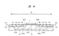
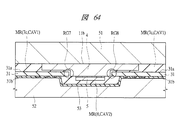
図56〜図67は、ステップS8のモールド工程の説明図である。このうち、図56は、金型51,52で配線基板31をクランプする前の段階を模式的に示す断面図(全体断面図)であり、図57は、金型51,52で配線基板31をクランプした段階を示す断面図(全体断面図)である。図58〜図61は、金型51,52で配線基板31をクランプした段階の要部断面図である。図58および図59には、1つの半導体装置領域32にほぼ対応する領域の断面図が示されており、図58は上記図1や図39および図42と同じ断面(すなわち上記A1−A1線や上記図40および図41のC1−C1線に対応する位置での断面)が示され、図59は、上記図2と同じ断面(すなわち上記A2−A2線や上記図40および図41のC2−C2線に対応する位置での断面)が示されている。また、図60は、図58における円で囲まれた領域RG5,RG6の部分拡大図に対応し、図61は、図59における円で囲まれた領域RG7,RG8の部分拡大図に対応する。なお、領域RG6は、上記領域RG1,RG3に対応し、領域RG5は、上記領域RG4に対応し、領域RG8は、上記領域RG2に対応している。   56 to 67 are explanatory diagrams of the molding process in step S8. 56 is a cross-sectional view (overall cross-sectional view) schematically showing a stage before the wiring board 31 is clamped by the molds 51 and 52, and FIG. 57 is a cross-sectional view of the wiring board 31 by the molds 51 and 52. It is sectional drawing (whole sectional drawing) which shows the step which clamped. 58 to 61 are cross-sectional views of the main parts at the stage where the wiring board 31 is clamped by the molds 51 and 52. 58 and 59 are cross-sectional views of regions substantially corresponding to one semiconductor device region 32. FIG. 58 is the same cross-section as FIG. 1, FIG. 39 and FIG. 42 (that is, the A1-A1 line). FIG. 59 shows the same cross section as FIG. 2 (that is, the A2-A2 line and C2 of FIG. 40 and FIG. 41). (Cross section at a position corresponding to line -C2). 60 corresponds to a partially enlarged view of the regions RG5 and RG6 surrounded by a circle in FIG. 58, and FIG. 61 corresponds to a partially enlarged view of the regions RG7 and RG8 surrounded by a circle in FIG. The region RG6 corresponds to the regions RG1 and RG3, the region RG5 corresponds to the region RG4, and the region RG8 corresponds to the region RG2.

ステップS8のモールド工程では、まず、ステップS1〜S7が行われて放熱板4が固定された(かしめられた)状態の配線基板31を、図56に示されるように、上金型である金型51と下金型である金型52との間に配置し、図57〜図59に示されるように、上下から金型51,52で挟んでクランプ(固定)する。この際、配線基板31の上面31aが上方を向いて金型(上金型)51と対向し、配線基板31の下面31bが下方を向いて金型(下金型)52と対向するように配線基板31を金型51,52で挟む。   In the molding process of step S8, first, steps S1 to S7 are performed, and the wiring board 31 in a state in which the heat sink 4 is fixed (crimped), as shown in FIG. It arrange | positions between the type | mold 51 and the metal mold | die 52 which is a lower metal mold | die, and as shown in FIGS. At this time, the upper surface 31 a of the wiring board 31 faces upward and faces the mold (upper mold) 51, and the lower surface 31 b of the wiring board 31 faces downward and faces the mold (lower mold) 52. The wiring board 31 is sandwiched between molds 51 and 52.

図56〜図59からも分かるように、配線基板31を金型51,52でクランプする際には、金型(下金型)52の上面(金型51や配線基板31と対向する側の主面)に、シート(フィルム、ラミネートフィルム)53を例えば吸着などで貼り付けた状態にし、金型(下金型)52と配線基板31の下面31bとが直接的に接触せずに間にシート53を介在させることが好ましい。このシート53は、金型(下金型)52よりも弾性を有しており、また、モールド工程の温度に耐える耐熱性も有しており、例えばポリイミド樹脂などの樹脂シートにより形成することができる。シート53を用いたことにより、配線基板31の下面31bの各半導体装置領域32の複数のバンプランドLAは、シート53に接するが、金型52と接するのは防止できるため、剛性の高い金型52で配線基板31の下面31bの複数のバンプランドLAが傷つくのを防止することができる。シート53は、ローラ54,55で巻き取りや送りを行うことができる。   As can be seen from FIGS. 56 to 59, when the wiring board 31 is clamped by the molds 51 and 52, the upper surface of the mold (lower mold) 52 (on the side facing the mold 51 and the wiring board 31). The sheet (film, laminate film) 53 is attached to the main surface) by, for example, adsorption, and the mold (lower mold) 52 and the lower surface 31b of the wiring board 31 are not in direct contact with each other. It is preferable to interpose the sheet 53. The sheet 53 is more elastic than the mold (lower mold) 52, and also has heat resistance that can withstand the temperature of the molding process, and can be formed of a resin sheet such as a polyimide resin. it can. By using the sheet 53, the plurality of bump lands LA in each semiconductor device region 32 on the lower surface 31b of the wiring board 31 are in contact with the sheet 53 but can be prevented from coming into contact with the mold 52. 52, it is possible to prevent the plurality of bump lands LA on the lower surface 31b of the wiring board 31 from being damaged. The sheet 53 can be wound and fed by rollers 54 and 55.

配線基板31を金型51,52でクランプすると、図57〜図62に示されるように、配線基板31の上面31aと金型(上金型)51との間にキャビティCAV1が形成され、配線基板31の下面31bと金型(下金型)52との間にキャビティCAV2が形成される。キャビティCAV1は、封止部7c形成用のキャビティ(空洞)であり、キャビティCAV2は、封止部8形成用のキャビティ(空洞)である。なお、封止部7cは、後で半導体装置領域32毎に分割されて上記封止部7となるため、キャビティCAV1は、封止部7形成用とみなすこともできる。   When the wiring board 31 is clamped by the molds 51 and 52, as shown in FIGS. 57 to 62, a cavity CAV1 is formed between the upper surface 31a of the wiring board 31 and the mold (upper mold) 51. A cavity CAV <b> 2 is formed between the lower surface 31 b of the substrate 31 and a mold (lower mold) 52. The cavity CAV1 is a cavity (cavity) for forming the sealing portion 7c, and the cavity CAV2 is a cavity (cavity) for forming the sealing portion 8. In addition, since the sealing part 7c is divided | segmented later for every semiconductor device area | region 32 and becomes the said sealing part 7, cavity CAV1 can also be considered for sealing part 7 formation.

キャビティCAV2は、配線基板31の下面31bと金型(下金型)52との間に形成されるが、シート53を用いた場合には、金型(下金型)52の上面に沿って配置されたシート53と配線基板31の下面31bとの間にキャビティCAV2が形成された状態となる。   The cavity CAV2 is formed between the lower surface 31b of the wiring substrate 31 and the mold (lower mold) 52. When the sheet 53 is used, the cavity CAV2 extends along the upper surface of the mold (lower mold) 52. A cavity CAV2 is formed between the disposed sheet 53 and the lower surface 31b of the wiring board 31.

配線基板31の下面31bと金型(下金型)52との間に形成されているキャビティCAV2は、配線基板31の下面31bの複数の半導体装置領域32の各々に対して、1つずつ設けられている。すなわち、1つの半導体装置領域32毎に1つのキャビティCAV2が設けられている。   One cavity CAV2 formed between the lower surface 31b of the wiring substrate 31 and the mold (lower mold) 52 is provided for each of the plurality of semiconductor device regions 32 on the lower surface 31b of the wiring substrate 31. It has been. That is, one cavity CAV 2 is provided for each semiconductor device region 32.

一方、配線基板31の上面31aと金型(上金型)51との間に形成されているキャビティCAV1は、配線基板31の上面31aの複数の半導体装置領域32全体を内包するように設けられている。すなわち、複数の半導体装置領域32に対して1つのキャビティCAV1が設けられている。但し、放熱板4の上記基材部11の裏面11bは、金型(上金型)51の下面に接している。   On the other hand, the cavity CAV1 formed between the upper surface 31a of the wiring board 31 and the mold (upper mold) 51 is provided so as to enclose the plurality of semiconductor device regions 32 on the upper surface 31a of the wiring board 31. ing. That is, one cavity CAV1 is provided for the plurality of semiconductor device regions 32. However, the back surface 11 b of the base material part 11 of the heat radiating plate 4 is in contact with the lower surface of the mold (upper mold) 51.

配線基板31を金型51,52でクランプした後、図62に示されるように、レジンゲート(レジンゲート口、樹脂注入口)56から、配線基板31の上面31aと金型(上金型)51との間に形成されているキャビティCAV1に、封止部7c,8形成用の樹脂材料MRを注入(導入)する。ここで、レジンゲート56はキャビティCAV1の横に配置されており、金型51,52はサイドゲート方式のモールド金型である。   After clamping the wiring board 31 with the molds 51 and 52, as shown in FIG. 62, the upper surface 31a of the wiring board 31 and the mold (upper mold) are formed from the resin gate (resin gate port, resin injection port) 56. The resin material MR for forming the sealing portions 7 c and 8 is injected (introduced) into the cavity CAV <b> 1 formed between the cavity 51 and the cavity 51. Here, the resin gate 56 is disposed beside the cavity CAV1, and the molds 51 and 52 are side gate type mold dies.

図62は、金型51,52のキャビティに樹脂材料MRを注入した状態(段階)を模式的に示す断面図(全体断面図)であり、図63〜図66は、金型51,52のキャビティに樹脂材料MRを注入した状態(段階)を示す要部断面図である。図63には、上記図58と同じ断面(すなわち上記A1−A1線や上記図40および図41のC1−C1線に対応する位置での断面)が示され、図64には、上記図59と同じ断面(すなわち上記A2−A2線や上記図40および図41のC2−C2線に対応する位置での断面)が示されている。また、図65には、上記図60と同じ断面が示され、図66には、上記図61と同じ断面が示されているので、図65は、図63における円で囲まれた領域RG5,RG6の部分拡大図に対応し、図66は、図64における円で囲まれた領域RG7,RG8の部分拡大図に対応する。   62 is a cross-sectional view (overall cross-sectional view) schematically showing a state (stage) in which the resin material MR is injected into the cavities of the molds 51 and 52. FIGS. It is principal part sectional drawing which shows the state (stage) which injected resin material MR in the cavity. 63 shows the same cross section as FIG. 58 (that is, the cross section at the position corresponding to the A1-A1 line and the C1-C1 line of FIGS. 40 and 41), and FIG. (That is, a cross section at a position corresponding to the line A2-A2 and the line C2-C2 in FIGS. 40 and 41). 65 shows the same cross section as in FIG. 60, and FIG. 66 shows the same cross section as in FIG. 61. Therefore, FIG. 65 shows a region RG5 surrounded by a circle in FIG. 66 corresponds to a partially enlarged view of RG6, and FIG. 66 corresponds to a partially enlarged view of regions RG7 and RG8 surrounded by a circle in FIG.

上記図59および図61にも示されるように、配線基板31の各貫通孔3の内壁とその貫通孔3に挿入された放熱板4の凸部12の側面12bとの間における少なくとも一箇所(好ましくは複数個所)に、貫通孔3の内壁と凸部12の側面12bとが離間しかつ配線基板31の上面31a側から下面31b側まで繋がる(連通する、貫通する)隙間部15がある。また、放熱板4は、支持部13の支持面13aが配線基板31の上面31aに接しているため、放熱板4の基材部11の主面11a(凸部12と支持部13のいずれも設けられていない領域)と配線基板31の上面31aとの間に、隙間18が形成されている。この隙間部15および隙間18は、上記ステップS5で配線基板31の各貫通孔3に放熱板4の凸部12を挿入した段階で形成され、この状態がステップS6で固定され、その後、ステップS8のモールド工程でレジンゲート56から樹脂材料MRを注入する前までは、隙間部15および隙間18は空洞として維持されている。   As shown in FIGS. 59 and 61, at least one location between the inner wall of each through hole 3 of the wiring board 31 and the side surface 12b of the convex portion 12 of the heat sink 4 inserted into the through hole 3 ( There are preferably gap portions 15 at a plurality of locations) in which the inner wall of the through-hole 3 and the side surface 12b of the convex portion 12 are separated from each other and are connected (communicated or penetrated) from the upper surface 31a side to the lower surface 31b side of the wiring board 31. Moreover, since the support surface 13a of the support part 13 is in contact with the upper surface 31a of the wiring board 31, the heat sink 4 has the main surface 11a of the base material part 11 of the heat sink 4 (both the convex part 12 and the support part 13). A gap 18 is formed between the area not provided) and the upper surface 31 a of the wiring substrate 31. The gap 15 and the gap 18 are formed at the stage where the protrusion 12 of the heat sink 4 is inserted into each through hole 3 of the wiring board 31 in step S5, and this state is fixed in step S6, and then step S8. Until the resin material MR is injected from the resin gate 56 in the molding step, the gap 15 and the gap 18 are maintained as cavities.

このため、配線基板31を金型51,52でクランプすると、配線基板31の上面31aと金型51との間に形成されるキャビティCAV1と、配線基板31の下面31bと金型52との間に形成されるキャビティCAV2との間は、放熱板4の基材部11の主面11aと配線基板31の上面31aとの間の隙間18と、放熱板4の凸部12の側面12bと貫通孔3の内壁との間の隙間部15とにより、繋がった状態となる。   For this reason, when the wiring board 31 is clamped by the molds 51 and 52, the cavity CAV1 formed between the upper surface 31a of the wiring board 31 and the mold 51, and the lower surface 31b of the wiring board 31 and the mold 52 are interposed. Between the main surface 11a of the base 11 of the heat radiating plate 4 and the upper surface 31a of the wiring board 31 and the side surface 12b of the convex portion 12 of the heat radiating plate 4 It will be in the connected state by the clearance gap part 15 between the inner walls of the hole 3. FIG.

キャビティCAV1とキャビティCAV2との間が隙間18と隙間部15とにより繋がっているため、レジンゲート56からキャビティCAV1内に注入された樹脂材料MRは、キャビティCAV1全体に行き渡ってキャビティCAV1内全体を充填するだけでなく、更に隙間18と隙間部15とを通って、配線基板31の下面31bと金型(下金型)52との間に形成されているキャビティCAV2内にも注入(導入)される。すなわち、隙間18と隙間部15とが樹脂材料MRの流路となり、レジンゲート56からキャビティCAV1内に樹脂材料MRを注入することで、キャビティCAV1内だけでなく、キャビティCAV2にも樹脂材料MRを充填することができる。また、キャビティCAV1において、放熱板4の基材部11の主面11aと配線基板31の上面31aとの間の隙間18も樹脂材料MRが充填された状態(樹脂材料MRで満たされた状態)となる。また、上記隙間部15も樹脂材料MRが充填された状態(樹脂材料MRで満たされた状態)となる。   Since the cavity CAV1 and the cavity CAV2 are connected by the gap 18 and the gap portion 15, the resin material MR injected into the cavity CAV1 from the resin gate 56 reaches the entire cavity CAV1 and fills the entire cavity CAV1. In addition, it is also injected (introduced) into the cavity CAV2 formed between the lower surface 31b of the wiring substrate 31 and the mold (lower mold) 52 through the gap 18 and the gap 15. The That is, the gap 18 and the gap 15 serve as a flow path for the resin material MR. By injecting the resin material MR from the resin gate 56 into the cavity CAV1, not only the cavity CAV1 but also the cavity CAV2 is filled with the resin material MR. Can be filled. In the cavity CAV1, the gap 18 between the main surface 11a of the base 11 of the heat sink 4 and the upper surface 31a of the wiring board 31 is also filled with the resin material MR (filled with the resin material MR). It becomes. The gap 15 is also filled with the resin material MR (filled with the resin material MR).

なお、キャビティCAV1,CAV2内に入っていた空気は、キャビティCAV1,CAV2に樹脂材料MRが充填されることに伴い、エアベント(エアベント口、ガスベント、ガス排気口)57から抜ける(排気される)ことになる。レジンゲート56およびエアベント57は、上金型である金型51側、すなわち配線基板31の上面31aと金型(上金型)51との間に形成される。   The air that has entered the cavities CAV1, CAV2 escapes (exhausts) from the air vent (air vent port, gas vent, gas exhaust port) 57 as the cavities CAV1, CAV2 are filled with the resin material MR. become. The resin gate 56 and the air vent 57 are formed between the upper mold 31, that is, between the upper surface 31 a of the wiring substrate 31 and the mold (upper mold) 51.

使用する樹脂材料MRは、例えば熱硬化性樹脂材料などからなり、フィラーなどを含むこともできる。例えば、フィラーを含むエポキシ樹脂などを用いて樹脂材料MRを形成することができるが、樹脂材料MRの流動性などは、キャビティCAV1内に注入した樹脂材料MRが上記隙間18と隙間部15とを通ってキャビティCAV2にも導入され得るように調整すればよい。   The resin material MR to be used is made of, for example, a thermosetting resin material, and can include a filler. For example, the resin material MR can be formed using an epoxy resin or the like containing a filler. However, the fluidity of the resin material MR is determined by the resin material MR injected into the cavity CAV1 between the gap 18 and the gap 15. It may be adjusted so that it can also be introduced into the cavity CAV2.

また、樹脂材料MRがフィラーを含む場合には、上記隙間18と隙間部15とは、樹脂材料MRに含まれるフィラーが通過できる寸法を有していることが好ましい。これにより、フィラーを含む樹脂材料MRをキャビティCAV1に導入すれば、上記隙間18および隙間部15を通じてキャビティCAV2に、フィラーを含む樹脂材料MRを導入することができる。このようにすることで、キャビティCAV1内の樹脂材料MRとキャビティCAV2内の樹脂材料MRとの組成(またはフィラー含有率)がほぼ同じになるため、封止部7c(7)と封止部8との組成(またはフィラー含有率)をほぼ同じにすることができる。   When the resin material MR contains a filler, the gap 18 and the gap 15 preferably have dimensions that allow the filler contained in the resin material MR to pass through. Thereby, if the resin material MR containing the filler is introduced into the cavity CAV1, the resin material MR containing the filler can be introduced into the cavity CAV2 through the gap 18 and the gap 15. By doing so, the composition (or filler content) of the resin material MR in the cavity CAV1 and the resin material MR in the cavity CAV2 become substantially the same, so the sealing portion 7c (7) and the sealing portion 8 And the composition (or filler content) can be made substantially the same.

キャビティCAV1,CAV2内に樹脂材料MRが充填された後、キャビティCAV1,CAV2内の樹脂材料MRを、加熱などにより硬化する。キャビティCAV1内の樹脂材料MRが硬化して封止部7cとなり、キャビティCAV2内の樹脂材料MRが硬化して封止部8となり、上記隙間部15も硬化した樹脂材料MRで満たされた状態となる。また、上記隙間18も硬化した樹脂材料MRで満たされた状態となるが、この隙間18を満たす樹脂材料MRも封止部7cの一部を構成する。その後、金型51,52を離型して、封止部7c,8が形成された配線基板31を取り出す。   After the cavities CAV1 and CAV2 are filled with the resin material MR, the resin material MR in the cavities CAV1 and CAV2 is cured by heating or the like. The resin material MR in the cavity CAV1 is cured to become the sealing portion 7c, the resin material MR in the cavity CAV2 is cured to become the sealing portion 8, and the gap portion 15 is also filled with the cured resin material MR. Become. Moreover, although the said clearance gap 18 will also be in the state filled with the hardened resin material MR, the resin material MR which fills this clearance gap 18 also comprises a part of sealing part 7c. Thereafter, the molds 51 and 52 are released, and the wiring board 31 on which the sealing portions 7c and 8 are formed is taken out.

封止部7cは、配線基板31の上面31aの複数の半導体装置領域32全体を覆うように形成されるが、各放熱板4の基材部11の裏面11bは封止部7cの上面から露出する。各放熱板4の基材部11の裏面11b上に樹脂バリが形成された場合には、ステップS8のモールド工程後に、バリ除去工程を行えばよい。   The sealing portion 7c is formed so as to cover the whole of the plurality of semiconductor device regions 32 on the upper surface 31a of the wiring board 31, but the back surface 11b of the base material portion 11 of each heat sink 4 is exposed from the upper surface of the sealing portion 7c. To do. When a resin burr is formed on the back surface 11b of the base material part 11 of each heat sink 4, a burr removing process may be performed after the molding process in step S8.

一方、配線基板31の下面31bの各半導体装置領域32において、バンプランドLAの配列領域上には封止部8は形成されず、バンプランドLAの配列領域よりも中央に形成される。従って、封止部8は、配線基板31の下面31bの各半導体装置領域32において、半導体チップ5、放熱板4の凸部12の主面12a、ボンディングワイヤBWおよびボンディングリードBLを覆うが、バンプランドLAは覆わないように形成される。   On the other hand, in each semiconductor device region 32 on the lower surface 31b of the wiring substrate 31, the sealing portion 8 is not formed on the arrangement region of the bump lands LA, but is formed in the center of the arrangement region of the bump lands LA. Accordingly, the sealing portion 8 covers the semiconductor chip 5, the main surface 12 a of the convex portion 12 of the heat sink 4, the bonding wire BW, and the bonding lead BL in each semiconductor device region 32 on the lower surface 31 b of the wiring substrate 31. The land LA is formed so as not to be covered.

<主要な特徴について>
本実施の形態では、放熱板4を用いたことにより、半導体装置の放熱特性を向上させることができる。半導体装置を製造する際には、この放熱板4を配線基板31に固定しないと、ワイヤボンディング工程やモールド工程、あるいは工程間の搬送などで、放熱板4が配線基板31から外れてしまう可能性がある。このため、半導体装置を製造する際には、放熱板4を配線基板31に固定する必要がある。
<About main features>
In the present embodiment, the use of the heat sink 4 can improve the heat dissipation characteristics of the semiconductor device. When manufacturing a semiconductor device, if the heat sink 4 is not fixed to the wiring board 31, the heat sink 4 may be detached from the wiring board 31 in a wire bonding process, a molding process, or conveyance between processes. There is. For this reason, when manufacturing a semiconductor device, it is necessary to fix the heat sink 4 to the wiring board 31.

本実施の形態では、放熱板4を配線基板31に固定するのに接着材を使用せず、かしめを用いて放熱板4を配線基板31に固定する。すなわち、上記ステップS6において、放熱板4の凸部12の主面12aの溝16を押し広げて、凸部12の側面12aの一部を配線基板31の貫通孔3の内壁と直接的に接触させることで、放熱板4を配線基板31にかしめて固定する。   In the present embodiment, the heat sink 4 is fixed to the wiring board 31 using caulking without using an adhesive to fix the heat sink 4 to the wiring board 31. That is, in step S <b> 6, the groove 16 of the main surface 12 a of the convex portion 12 of the heat radiating plate 4 is expanded to directly contact a part of the side surface 12 a of the convex portion 12 with the inner wall of the through hole 3 of the wiring board 31. By doing so, the heat sink 4 is caulked and fixed to the wiring board 31.

本実施の形態とは異なり、放熱板4を配線基板3に固定するのに接着材を使用した場合には、配線基板31の貫通孔3の寸法(内寸)と放熱板4の凸部12の寸法(外形寸法)とが変動すると、接着材の不足または過剰を招いてしまい、放熱板4の固定が上手くいかなくなる虞がある。また、放熱板4固定用の接着材が、配線基板31の下面31bにおいて貫通孔3の周囲に溢れてボンディングリードBLに付着してしまい、ワイヤボンディング不良を招く虞もある。また、接着材で固定する場合、放熱板4の凸部12を配線基板31の貫通孔3内に挿入する際、放熱板4の挿入性を考慮して、凸部12の側面12bと貫通孔3の内壁と間に隙間が形成されるため、放熱板4の保持力が低くなる虞がある。これらは、半導体装置の信頼性を低下させてしまう。   Unlike the present embodiment, when an adhesive is used to fix the heat sink 4 to the wiring board 3, the dimension (inner dimension) of the through hole 3 of the wiring board 31 and the convex portion 12 of the heat sink 4. If the dimensions (outer dimensions) vary, there will be a shortage or excess of the adhesive, and there is a possibility that the heat sink 4 will not be fixed properly. In addition, the adhesive for fixing the heat sink 4 overflows around the through hole 3 on the lower surface 31b of the wiring board 31 and adheres to the bonding lead BL, which may cause a wire bonding failure. Further, when fixing with the adhesive, when inserting the convex portion 12 of the heat sink 4 into the through hole 3 of the wiring substrate 31, the side surface 12 b of the convex portion 12 and the through hole are taken into consideration in consideration of the insertability of the heat sink 4. Since a gap is formed between the inner walls of the heat sink 3, the holding power of the heat sink 4 may be reduced. These deteriorate the reliability of the semiconductor device.

それに対して、本実施の形態では、凸部12の溝16を押し広げることで放熱板4を配線基板31にかしめる(固定する)ため、配線基板31の貫通孔3の寸法(内寸)と放熱板4の凸部12の寸法(外形寸法)とが多少変動したとしても、放熱板4を固定しやすい。また、放熱板4固定用の接着材を使用しないため、その接着材がボンディングリードBLに付着することがないため、ワイヤボンディング不良の発生を防止できる。また、配線基板31の貫通孔3と放熱板4の凸部12の寸法精度(クリアランス)を、放熱板4の固定に接着材を使用する場合に比べて低く設定することもでき、半導体装置の製造コストを低減することができる。   On the other hand, in the present embodiment, the heat sink 4 is caulked (fixed) to the wiring board 31 by expanding the groove 16 of the convex portion 12, so the dimension (inner dimension) of the through hole 3 of the wiring board 31. Even if the dimensions (outer dimensions) of the projections 12 of the heat sink 4 vary somewhat, it is easy to fix the heat sink 4. Further, since the adhesive for fixing the heat sink 4 is not used, the adhesive does not adhere to the bonding lead BL, so that it is possible to prevent the occurrence of defective wire bonding. In addition, the dimensional accuracy (clearance) of the through hole 3 of the wiring board 31 and the convex portion 12 of the heat sink 4 can be set lower than when an adhesive is used to fix the heat sink 4. Manufacturing cost can be reduced.

また、本実施の形態では、放熱板4の凸部12の溝16を押し広げることで放熱板4を配線基板31にかしめている(固定している)ため、上記図54および図60に示されるように、凸部12の側面12bのうち、主面11aに近い領域は、配線基板31の貫通孔3の内壁に接しているが、基材部11に近い領域は、配線基板31の貫通孔3の内壁との間に、若干の隙間19がある。すなわち、隙間部15を除く凸部12の側面12bは、配線基板31の貫通孔3の内壁に接する領域(主面12aに近い領域)と接しない領域とがある。このため、ステップS8のモールド工程を行うと、図65に示されるように、放熱板4の凸部12の側面12bと貫通孔3の内壁との間の隙間19にも樹脂材料MRが充填される。すなわち、放熱板4の凸部12の側面12bのうちの貫通孔3の内壁と直接接していない部分と貫通孔3の内壁との間にも樹脂材料MRが充填されるのである。この隙間19への樹脂材料MRの充填は、上記隙間18や上記隙間部15から隙間19へ樹脂材料MRが侵入することによって達成され得る。このため、ステップS8のモールド工程を行って封止部7c,8を形成すると、隙間部15を除く放熱板4の凸部12の側面12bのうち、一部(主面12aに近い領域)は配線基板31の貫通孔3の内壁に接し、他の部分は、配線基板31の貫通孔3の内壁との間に硬化した樹脂材料MRが介在した状態となり、この状態は製造された半導体装置1においても維持されている。隙間19は、上記隙間18や隙間部15の寸法よりも小さく、樹脂材料MRが含んでいるフィラーが通過できなくともよい。   Further, in the present embodiment, the heat sink 4 is caulked (fixed) to the wiring board 31 by expanding the groove 16 of the convex portion 12 of the heat sink 4. As shown, the region near the main surface 11 a of the side surface 12 b of the convex portion 12 is in contact with the inner wall of the through hole 3 of the wiring substrate 31, but the region close to the base material portion 11 penetrates the wiring substrate 31. There is a slight gap 19 between the inner wall of the hole 3. That is, the side surface 12 b of the convex portion 12 excluding the gap portion 15 has a region that does not contact the region (region close to the main surface 12 a) that contacts the inner wall of the through hole 3 of the wiring substrate 31. Therefore, when the molding process of step S8 is performed, the resin material MR is also filled in the gap 19 between the side surface 12b of the convex portion 12 of the heat sink 4 and the inner wall of the through hole 3 as shown in FIG. The That is, the resin material MR is also filled between the portion of the side surface 12 b of the convex portion 12 of the heat radiating plate 4 that is not in direct contact with the inner wall of the through hole 3 and the inner wall of the through hole 3. The filling of the resin material MR into the gap 19 can be achieved by the resin material MR entering the gap 19 from the gap 18 or the gap portion 15. For this reason, when the molding step of step S8 is performed to form the sealing portions 7c and 8, a part (region close to the main surface 12a) of the side surface 12b of the convex portion 12 of the heat radiating plate 4 excluding the gap portion 15 is formed. The hardened resin material MR is interposed between the inner wall of the through hole 3 of the wiring board 31 and the other part between the inner wall of the through hole 3 of the wiring board 31, and this state is the manufactured semiconductor device 1. Is also maintained. The gap 19 is smaller than the dimensions of the gap 18 and the gap portion 15, and the filler contained in the resin material MR may not pass therethrough.

このように、本実施の形態では、放熱板4の凸部12の溝16を押し広げることで放熱板4を配線基板31にかしめている(固定している)ため、放熱板4の凸部12の側面12bの全面が貫通孔3の内壁と接している訳ではなく、上記隙間19に樹脂材料MRが入って(充填されて)、放熱板4と配線基板2(31)との密着性を向上させている。このため、製造された半導体装置1において、放熱板4と配線基板2との密着性(接着性)を向上させることができるため、配線基板2や封止部7,8に放熱板4をしっかりと固定することができる。従って、半導体装置1の信頼性を向上させることができる。   As described above, in the present embodiment, the heat sink 4 is crimped (fixed) to the wiring board 31 by expanding the groove 16 of the protrusion 12 of the heat sink 4. The entire surface of the side surface 12b of 12 is not in contact with the inner wall of the through-hole 3, but the resin material MR is filled (filled) in the gap 19, and the adhesion between the heat sink 4 and the wiring board 2 (31) Has improved. For this reason, in the manufactured semiconductor device 1, since the adhesiveness (adhesiveness) between the heat sink 4 and the wiring board 2 can be improved, the heat sink 4 is firmly attached to the wiring board 2 and the sealing portions 7 and 8. And can be fixed. Therefore, the reliability of the semiconductor device 1 can be improved.

また、ステップS7のワイヤボンディング工程は、配線基板31の下面31bを上方に向けた状態で行い、ステップS8のモールド工程は、配線基板31の上面31aを上方に向けた状態で行うため、ステップS7からステップS8の間に、配線基板31を上下反転させる。本実施の形態では、放熱板4の凸部12の溝16を押し広げることで放熱板4を配線基板31にかしめている(固定している)ため、ステップS7からステップS8の間に配線基板31を上下反転させて、ステップS8のモールド工程を配線基板31の上面31aを上方に向けた状態で行っても、放熱板4が配線基板31から外れてしまうのを防止することができる。このため、半導体装置の製造工程を的確に行うことができる。   Further, the wire bonding process of step S7 is performed with the lower surface 31b of the wiring board 31 facing upward, and the molding process of step S8 is performed with the upper surface 31a of the wiring board 31 facing upward, so step S7. To step S8, the wiring board 31 is turned upside down. In the present embodiment, the heat sink 4 is caulked (fixed) to the wiring board 31 by pushing the groove 16 of the convex portion 12 of the heat sink 4, so that the wiring board is between step S7 and step S8. Even if 31 is turned upside down and the molding process of step S8 is performed with the upper surface 31a of the wiring board 31 facing upward, it is possible to prevent the heat sink 4 from being detached from the wiring board 31. For this reason, the manufacturing process of a semiconductor device can be performed accurately.

また、本実施の形態では、外部接続端子(ここでは半田ボール9)形成側の主面である配線基板2の下面2b側に半導体チップ5を配置している。このため、配線基板2(31)の下面2b(31b)側に封止部8を形成する必要があるが、外部端子形成用の端子であるバンプランドLA上には、封止部8を形成してはいけない。このため、配線基板2(31)の下面2b(31b)側の封止部8は、個々の半導体装置領域32に対してそれぞれ形成する必要がある。   Further, in the present embodiment, the semiconductor chip 5 is arranged on the lower surface 2b side of the wiring board 2 which is the main surface on the external connection terminal (here, solder ball 9) formation side. For this reason, it is necessary to form the sealing portion 8 on the lower surface 2b (31b) side of the wiring board 2 (31), but the sealing portion 8 is formed on the bump land LA which is a terminal for forming an external terminal. Do not. For this reason, the sealing portion 8 on the lower surface 2b (31b) side of the wiring board 2 (31) needs to be formed for each semiconductor device region 32.

そこで、本実施の形態では、ステップS8のモールド工程において、配線基板31の上面31a側(すなわちキャビティCAV1)に供給した樹脂材料MRを、上記隙間部15(および上記隙間18)を通じて配線基板31の下面31b側(すなわちキャビティCAV2)にも供給し、それによって、配線基板31の上面31a側に封止部7cを、配線基板31の下面31b側に封止部8を、それぞれ形成している。これにより、配線基板31の下面31b側の封止部8を、バンプランドLAを覆わないように、容易かつ的確に形成することができる。また、配線基板31の上面31a側の封止部7cと、配線基板31の下面31b側の封止部8とを一度に形成することができるため、半導体装置の製造工程数を抑制することができる。   Therefore, in the present embodiment, the resin material MR supplied to the upper surface 31a side (that is, the cavity CAV1) of the wiring board 31 in the molding process of step S8 is passed through the gap 15 (and the gap 18) of the wiring board 31. This is also supplied to the lower surface 31b side (that is, the cavity CAV2), thereby forming the sealing portion 7c on the upper surface 31a side of the wiring substrate 31 and the sealing portion 8 on the lower surface 31b side of the wiring substrate 31, respectively. Thereby, the sealing portion 8 on the lower surface 31b side of the wiring substrate 31 can be easily and accurately formed so as not to cover the bump land LA. Further, since the sealing portion 7c on the upper surface 31a side of the wiring substrate 31 and the sealing portion 8 on the lower surface 31b side of the wiring substrate 31 can be formed at a time, the number of manufacturing steps of the semiconductor device can be suppressed. it can.

また、配線基板2の上面2a側の封止部7と配線基板2の下面2b側の封止部8とが、隙間部15内を満たす樹脂材料MRを介して一体的に繋がった状態となるため、半導体装置1における封止部7,8の剥離(配線基板2からの剥離)を抑制または防止することができる。このため、半導体装置の信頼性を更に向上させることができる。   Further, the sealing portion 7 on the upper surface 2 a side of the wiring substrate 2 and the sealing portion 8 on the lower surface 2 b side of the wiring substrate 2 are integrally connected via the resin material MR filling the gap portion 15. Therefore, peeling of the sealing portions 7 and 8 (peeling from the wiring board 2) in the semiconductor device 1 can be suppressed or prevented. For this reason, the reliability of the semiconductor device can be further improved.

また、配線基板31の上面31a側(のキャビティCAV1)に供給した樹脂材料MRを、上記隙間部15(および上記隙間18)を通じて配線基板31の下面31b側(のキャビティCAV2)に供給する際に、放熱板4の凸部12の側面12bと貫通孔3の内壁との間の上記隙間19にも樹脂材料MRが充填されやすいため、放熱板4と配線基板2(31)との密着性を向上させることができる。このため、半導体装置1の信頼性を向上させることができる。   When the resin material MR supplied to the upper surface 31a side (cavity CAV1) of the wiring board 31 is supplied to the lower surface 31b side (cavity CAV2) of the wiring board 31 through the gap 15 (and the gap 18). Since the resin material MR is also easily filled in the gap 19 between the side surface 12b of the convex portion 12 of the heat sink 4 and the inner wall of the through hole 3, adhesion between the heat sink 4 and the wiring board 2 (31) is improved. Can be improved. For this reason, the reliability of the semiconductor device 1 can be improved.

また、各半導体装置領域32に対して(すなわち1つの放熱板4に対して)、上記隙間部15は少なくとも1つ設けるが、複数設けることが好ましい。図67は、キャビティCAV2に樹脂材料MRが充填される途中の段階を示す断面図である。   Further, at least one gap portion 15 is provided for each semiconductor device region 32 (that is, for one heat radiating plate 4), but a plurality of gap portions 15 are preferably provided. FIG. 67 is a cross-sectional view showing a stage in the middle of filling the cavity CAV2 with the resin material MR.

上記レジンゲート56からキャビティCAV1に注入された樹脂材料MRは、隙間18と隙間部15を通ってキャビティCAV2に導入される。このとき、個々の半導体装置領域32(のキャビティCAV2)に対して隙間部15が複数あると、複数の隙間部15のうち、レジンゲート56に近い側の隙間部15aからキャビティCAV2に樹脂材料MRが導入され、キャビティCAV2内の空気は他の隙間部(エアベント57に近い隙間部)15bからキャビティCAV1へ排気され、更に上記エアベント57から金型51,52の外に排気される。   The resin material MR injected from the resin gate 56 into the cavity CAV1 is introduced into the cavity CAV2 through the gap 18 and the gap 15. At this time, if there are a plurality of gaps 15 with respect to each semiconductor device region 32 (cavity CAV2 thereof), the resin material MR enters the cavity CAV2 from the gap 15a closer to the resin gate 56 among the plurality of gaps 15. Is introduced, and the air in the cavity CAV2 is exhausted to the cavity CAV1 from the other gap part (gap part close to the air vent 57) 15b, and is further exhausted from the air vent 57 to the outside of the molds 51 and 52.

このため、各半導体装置領域32に対して(すなわち1つの放熱板4に対して)、上記隙間部15を複数設ければ、それら複数の隙間部15のうち、キャビティCAV2への樹脂注入口(レジンゲート)として機能するものと、キャビティCAV2からのガス排気口(エアベント)として機能するものとが、それぞれ1つ以上確保される。これにより、キャビティCAV1に注入された樹脂材料MRを、隙間部15を介してキャビティCAV2に的確に導入することができ、封止部8を的確に形成できるようになる。   For this reason, if a plurality of gaps 15 are provided for each semiconductor device region 32 (that is, for one heat sink 4), a resin injection port (into the cavity CAV2 among the plurality of gaps 15) ( One or more that functions as a resin gate and one that functions as a gas exhaust port (air vent) from the cavity CAV2 are secured. Accordingly, the resin material MR injected into the cavity CAV1 can be accurately introduced into the cavity CAV2 through the gap portion 15, and the sealing portion 8 can be accurately formed.

また、各半導体装置領域32に対して(すなわち1つの放熱板4に対して)設けられた複数の隙間部15は、それぞれほぼ同じ寸法とすることが好ましい。これは、隙間部15(ここでは隙間部15a)からキャビティCAV2内に導入された樹脂材料MRは、他の隙間部15(ここでは隙間部15b)からキャビティCAV1に戻って、封止部7cや他の封止部8を形成するために使用できるためである。こうすることで、封止部7c,8を形成しやすくなる。このため、キャビティCAV2に樹脂材料MRが注入される際には、樹脂注入口(レジンゲート)として機能する隙間部15(ここでは隙間部15a)とガス排気口(エアベント)として機能する隙間部15(ここでは隙間部15b)との寸法がほぼ同じであり、封止部8はスルーモールドで形成されることになる。一方、上記レジンゲート56は樹脂材料MRが通過できるが、エアベント57は、排気用であり、樹脂材料MRはほとんど通過しないようにするため、上記エアベント57(の隙間)は、上記レジンゲート56、上記隙間部15および上記隙間18よりも小さい。   Moreover, it is preferable that the plurality of gaps 15 provided for each semiconductor device region 32 (that is, for one heat sink 4) have substantially the same dimensions. This is because the resin material MR introduced into the cavity CAV2 from the gap portion 15 (here, the gap portion 15a) returns from the other gap portion 15 (here, the gap portion 15b) to the cavity CAV1, and the sealing portion 7c or This is because it can be used to form another sealing portion 8. By doing so, the sealing portions 7c and 8 are easily formed. Therefore, when the resin material MR is injected into the cavity CAV2, the gap portion 15 (here, the gap portion 15a) that functions as a resin injection port (resin gate) and the gap portion 15 that functions as a gas exhaust port (air vent). The dimensions with (here, the gap portion 15b) are substantially the same, and the sealing portion 8 is formed by through molding. On the other hand, although the resin material MR can pass through the resin gate 56, the air vent 57 is used for exhaustion, and the resin material MR hardly passes therethrough. It is smaller than the gap 15 and the gap 18.

また、配線基板31(2)の貫通孔3の平面形状と放熱板4の凸部12の平面形状とを、それぞれ矩形状とし、隙間部15を、この矩形状の四隅の位置(上記四隅17の位置)にそれぞれ形成すれば、より好ましい。これにより、キャビティCAV1に注入した樹脂材料MRを、隙間部15を通してキャビティCAV2にバランスよく導入することができ、封止部8をより的確に形成できるようになる。   Further, the planar shape of the through-hole 3 of the wiring board 31 (2) and the planar shape of the convex portion 12 of the heat sink 4 are each rectangular, and the gap portion 15 is positioned at the four corners of the rectangular shape (the four corners 17). It is more preferable to form them at the respective positions. As a result, the resin material MR injected into the cavity CAV1 can be introduced into the cavity CAV2 with a good balance through the gap portion 15, and the sealing portion 8 can be formed more accurately.

(実施の形態2)
上記実施の形態1で説明した製造工程では、放熱板4の凸部12上に半導体チップ5を搭載してから、半導体チップ5が搭載された放熱板4を配線基板31の貫通孔3内に配置していた。本実施の形態では、放熱板4の凸部12に半導体チップ5を搭載する前に、放熱板4を配線基板31の貫通孔3内に配置し、その後、配線基板31の貫通孔3内に配置された放熱板4の凸部12に半導体チップ5を搭載する。この場合を、図68〜図74を参照して説明する。
(Embodiment 2)
In the manufacturing process described in the first embodiment, after the semiconductor chip 5 is mounted on the convex portion 12 of the heat sink 4, the heat sink 4 on which the semiconductor chip 5 is mounted is placed in the through hole 3 of the wiring substrate 31. It was arranged. In the present embodiment, before the semiconductor chip 5 is mounted on the convex portion 12 of the heat sink 4, the heat sink 4 is disposed in the through hole 3 of the wiring board 31, and then in the through hole 3 of the wiring board 31. The semiconductor chip 5 is mounted on the convex portion 12 of the arranged heat sink 4. This case will be described with reference to FIGS.

図68は、本実施の形態の半導体装置1の他の製造工程を示す工程フロー図であり、上記実施の形態1の上記図22に対応するものである。図69〜図74は、本実施の形態の半導体装置1の製造工程中の平面図または断面図である。図69〜図74のうち、図69、図71および図73は平面図であり、図70、図72および図74は断面図である。   FIG. 68 is a process flowchart showing another manufacturing process of the semiconductor device 1 of the present embodiment, and corresponds to FIG. 22 of the first embodiment. 69 to 74 are plan views or cross-sectional views during the manufacturing process of the semiconductor device 1 of the present embodiment. 69 to 74, FIGS. 69, 71, and 73 are plan views, and FIGS. 70, 72, and 74 are sectional views.

まず、ステップS1,S2で、配線基板31およびフレーム41を準備する。配線基板31を先に準備しても、フレーム41を先に準備しても、あるいは配線基板31およびフレーム41を同時に準備してもよい。   First, in steps S1 and S2, the wiring board 31 and the frame 41 are prepared. The wiring board 31 may be prepared first, the frame 41 may be prepared first, or the wiring board 31 and the frame 41 may be prepared simultaneously.

次に、本実施の形態では、ダイボンディング工程を行うことなく、ステップS4で、フレーム41の各放熱板4を、フレーム41のフレーム枠42から切断して分離する。これにより、放熱板4が個片化される。   Next, in the present embodiment, without performing the die bonding process, each heat radiation plate 4 of the frame 41 is cut and separated from the frame frame 42 of the frame 41 in step S4. Thereby, the heat sink 4 is separated into pieces.

次に、図69および70に示されるように、ステップS5で放熱板4(ここでは半導体チップ5が搭載されていない放熱板4)の凸部12を、配線基板31の各半導体装置領域32の貫通孔3内に配置(挿入)し、それから、ステップS6で各放熱板4(の凸部12)を配線基板31(の各貫通孔3)にかしめることにより、各放熱板4を配線基板31に固定する。図69および図70は、ステップS6まで行われた段階を示す平面図(図69)および断面図(図70)である。図69には、上記図35と同じ領域(すなわち3つの半導体装置領域32)が示され、配線基板31の下面31b側が示されている。図70には、上記図37に対応する断面図(すなわち図69のC1−C1線の断面図)が示されている。   Next, as shown in FIGS. 69 and 70, in step S <b> 5, the protrusions 12 of the heat sink 4 (here, the heat sink 4 on which the semiconductor chip 5 is not mounted) are moved to the respective semiconductor device regions 32 of the wiring board 31. Each heat sink 4 is placed (inserted) in the through hole 3 and then each heat sink 4 (projection 12) is caulked to the wiring board 31 (each through hole 3) in step S6. Fix to 31. FIGS. 69 and 70 are a plan view (FIG. 69) and a cross-sectional view (FIG. 70) showing the steps performed up to step S6. 69 shows the same region (that is, three semiconductor device regions 32) as FIG. 35, and shows the lower surface 31b side of the wiring board 31. FIG. 70 is a sectional view corresponding to FIG. 37 (that is, a sectional view taken along line C1-C1 in FIG. 69).

半導体チップ5が放熱板4上に搭載されていないこと以外、ステップS5の放熱板4の配置工程およびステップS6の放熱板4の固定(かしめ)工程は、上記実施の形態1で説明したのと同様にして行われるので、ここではその詳細な説明は省略する。従って、ステップS6の放熱板4の固定(かしめ)工程までを行った段階では、配線基板31にかしめられた固定された各放熱板4の凸部12上には、半導体チップ5は搭載されていない。   Except that the semiconductor chip 5 is not mounted on the heat sink 4, the step of arranging the heat sink 4 in step S <b> 5 and the step of fixing (caulking) the heat sink 4 in step S <b> 6 have been described in the first embodiment. Since it is performed in the same manner, detailed description thereof is omitted here. Accordingly, at the stage where the heat sink 4 is fixed (caulked) in step S6, the semiconductor chip 5 is mounted on the convex portion 12 of each heat sink 4 fixed to the wiring board 31. Absent.

次に、ステップS3のダイボンディング工程を行って、配線基板31に固定された(かしめられた)各放熱板4の凸部12の主面12a上に、半導体チップ5を接合材14を介して搭載して接合する。本実施の形態では、ステップS3のダイボンディング工程は、次のようにして行うことができる。   Next, the die bonding process of step S3 is performed, and the semiconductor chip 5 is placed on the main surface 12a of the convex portion 12 of each heat sink 4 fixed (crimped) to the wiring board 31 via the bonding material 14. Mount and join. In the present embodiment, the die bonding process of step S3 can be performed as follows.

すなわち、図71(上記図69と同じ領域の平面図)および図72(上記図70に対応する断面図)に示されるように、配線基板31の各半導体装置領域32の貫通孔3内に配置されて固定された各放熱板4の凸部12の主面12a上に、導電性のペースト材、好ましくは銀ペースト14bを塗布する。それから、図73(上記図69および図71と同じ領域の平面図)および図74(上記図70および図72に対応する断面図)に示されるように、配線基板31の各半導体装置領域32の貫通孔3内に配置されて固定された各放熱板4の凸部12の主面12a上に、半導体チップ5を銀ペースト14bを介して搭載する。その後、加熱処理などを行って、銀ペースト14bを硬化させる。これにより、半導体チップ5の搭載時にはペースト状態であった銀ペースト14bが硬化し、硬化した銀ペースト14bによって、半導体チップ5が放熱板4の凸部12に接合されて固定される。この硬化した銀ペースト14bが、上記接着材14となる。なお、ステップS5のダイボンディング工程は、図71〜図74からも分かるように、配線基板31の下面31bが上方を向いた状態で行う。   That is, as shown in FIG. 71 (a plan view of the same region as FIG. 69) and FIG. 72 (a cross-sectional view corresponding to FIG. 70), it is arranged in the through hole 3 of each semiconductor device region 32 of the wiring board 31. Then, a conductive paste material, preferably a silver paste 14b, is applied onto the main surface 12a of the convex portion 12 of each heat sink 4 fixed. Then, as shown in FIG. 73 (plan view of the same region as in FIGS. 69 and 71) and FIG. 74 (cross-sectional view corresponding to FIGS. 70 and 72), each semiconductor device region 32 of the wiring board 31 is formed. The semiconductor chip 5 is mounted on the main surface 12a of the convex portion 12 of each heat radiating plate 4 arranged and fixed in the through hole 3 via a silver paste 14b. Thereafter, heat treatment or the like is performed to cure the silver paste 14b. Thereby, the silver paste 14b which was in a paste state when the semiconductor chip 5 is mounted is cured, and the semiconductor chip 5 is bonded and fixed to the convex portion 12 of the heat sink 4 by the cured silver paste 14b. This hardened silver paste 14 b becomes the adhesive 14. The die bonding process in step S5 is performed with the lower surface 31b of the wiring board 31 facing upward, as can be seen from FIGS.

これ以降の工程は、上記実施の形態1で説明した製造工程と同様である。すなわち、上記ステップS7のワイヤボンディング工程を行い、上記ステップS8のモールド工程を行い、上記ステップS9の半田ボール9接続工程を行い、上記ステップS10の切断工程を行う。このようにして、上記図1〜図10に示されるような半導体装置1が製造される。   The subsequent steps are the same as the manufacturing steps described in the first embodiment. That is, the wire bonding process of step S7 is performed, the molding process of step S8 is performed, the solder ball 9 connection process of step S9 is performed, and the cutting process of step S10 is performed. In this way, the semiconductor device 1 as shown in FIGS. 1 to 10 is manufactured.

樹脂基板からなる配線基板31は、金属材料からなるフレーム41(放熱板4)に比べて高温の熱処理への耐久性が低い。上記実施の形態1で説明した製造工程では、ステップS5,S6で配線基板31に放熱板4を配置して固定する前に、ステップS3で放熱板4上に半導体チップ5を接合しているため、ステップS3の半導体チップ5の接合工程の熱処理時には、配線基板31は加熱されない。このため、配線基板31の耐熱性を気にすることなく、ステップS3の半導体チップ5の接合工程の熱処理に高温の熱処理を行うことができる。従って、ステップS3の半導体チップ5の接合工程の熱処理に高温の熱処理を行う場合、例えば、バンプランドLA上に形成する外部端子(ここでは半田ボール9)に用いる半田よりも高融点の半田14aを用いて半導体チップ5を放熱板4に接合する場合には、上記実施の形態1で説明した製造工程を適用すれば、ステップS3の半導体チップ5の接合工程の半田リフロー時に配線基板31がダメージを受けないので、好適である。   The wiring substrate 31 made of a resin substrate is less durable to high-temperature heat treatment than the frame 41 (heat radiating plate 4) made of a metal material. In the manufacturing process described in the first embodiment, the semiconductor chip 5 is bonded onto the heat sink 4 in step S3 before the heat sink 4 is arranged and fixed to the wiring board 31 in steps S5 and S6. During the heat treatment in the bonding process of the semiconductor chip 5 in step S3, the wiring board 31 is not heated. For this reason, high temperature heat treatment can be performed in the heat treatment of the bonding process of the semiconductor chip 5 in step S3 without worrying about the heat resistance of the wiring board 31. Therefore, when high-temperature heat treatment is performed as the heat treatment in the bonding process of the semiconductor chip 5 in step S3, for example, a solder 14a having a melting point higher than that of the solder used for the external terminal (here, the solder ball 9) formed on the bump land LA is used. When the semiconductor chip 5 is bonded to the heat sink 4 by using the manufacturing process described in the first embodiment, the wiring board 31 is damaged during the solder reflow in the bonding process of the semiconductor chip 5 in step S3. Since it does not receive, it is suitable.

すなわち、半田ボール9に鉛フリー半田を使用した場合の半導体装置1の実装時(上記実装基板21などへの実装時)の半田リフロー温度は例えば220℃程度であり、半田ボール9に鉛含有半田を使用した場合の半導体装置1の実装時(上記実装基板21などへの実装時)の半田リフロー温度は例えば180℃程度である。一方、半田14aに高温半田を用いた場合のステップS3での半田リフロー温度は、350〜400℃程度が望ましいが、このような高温には配線基板31が耐えられない可能性があるが、上記実施の形態1で説明した製造工程では、ステップS5,S6で配線基板31に放熱板4を配置して固定する前に、ステップS3で放熱板4上に半導体チップ5を接合しているため、半田リフロー時の配線基板31の耐久性の問題が無くなる。   That is, when lead-free solder is used for the solder balls 9, the solder reflow temperature when the semiconductor device 1 is mounted (when mounted on the mounting substrate 21 or the like) is about 220 ° C., for example. When the semiconductor device 1 is used, the solder reflow temperature when mounting the semiconductor device 1 (when mounting on the mounting substrate 21 or the like) is about 180 ° C., for example. On the other hand, the solder reflow temperature in step S3 when high-temperature solder is used for the solder 14a is preferably about 350 to 400 ° C. The wiring board 31 may not be able to withstand such a high temperature. In the manufacturing process described in the first embodiment, the semiconductor chip 5 is bonded onto the heat sink 4 in step S3 before the heat sink 4 is arranged and fixed to the wiring board 31 in steps S5 and S6. The problem of durability of the wiring board 31 during solder reflow is eliminated.

また、接着材14として半田を用いれば、銀ペーストを用いる場合に比べて、接着材14の熱伝導性が高くなるため、半導体チップ5から放熱板4への熱伝導性をより高めて、半導体装置1の放熱性をより向上させることができる。   In addition, when solder is used as the adhesive 14, the thermal conductivity of the adhesive 14 is higher than when silver paste is used. Therefore, the thermal conductivity from the semiconductor chip 5 to the heat radiating plate 4 is further increased, and the semiconductor The heat dissipation of the device 1 can be further improved.

一方、本実施の形態で説明した製造工程では、ステップS5,S6で配線基板31に放熱板4を配置して固定した後に、ステップS3で放熱板4上に半導体チップ5を接合しているため、ステップS3の半導体チップ5の接合工程の熱処理時に、配線基板31は加熱される。このため、本実施の形態で説明した製造工程を行う場合には、ステップS3の半導体チップ5の接合工程の熱処理にあまり高温の熱処理を行なわないことが好ましく、上述のように、銀ペースト14bを用いて半導体チップ5を放熱板4に接合すれば、ステップS3の半導体チップ5の接合工程の接着材(銀ペースト14b)の硬化用熱処理時に配線基板31がダメージを受けないので、好適である。   On the other hand, in the manufacturing process described in the present embodiment, the semiconductor chip 5 is bonded onto the heat sink 4 in step S3 after the heat sink 4 is arranged and fixed on the wiring board 31 in steps S5 and S6. The wiring substrate 31 is heated during the heat treatment in the bonding process of the semiconductor chip 5 in step S3. For this reason, when the manufacturing process described in the present embodiment is performed, it is preferable not to perform a heat treatment at a very high temperature in the bonding process of the semiconductor chip 5 in step S3. If the semiconductor chip 5 is bonded to the heat dissipation plate 4 by using, it is preferable because the wiring board 31 is not damaged during the heat treatment for curing the adhesive (silver paste 14b) in the bonding process of the semiconductor chip 5 in step S3.

(実施の形態3)
図75および図76は、本実施の形態の半導体装置1aの断面図(側面断面図)であり、上記実施の形態1の上記図1および図2にそれぞれ対応するものである。
(Embodiment 3)
75 and 76 are cross-sectional views (side cross-sectional views) of the semiconductor device 1a of the present embodiment, and correspond to FIGS. 1 and 2 of the first embodiment, respectively.

上記実施の形態1の半導体装置1は、放熱板4の凸部12の主面12aが、配線基板2の下面2bと略同一平面上にあり、放熱板4の凸部12の主面12aの高さ位置と、配線基板2の下面2bの高さ位置とがほぼ同じであった。   In the semiconductor device 1 of the first embodiment, the main surface 12a of the convex portion 12 of the heat sink 4 is substantially flush with the lower surface 2b of the wiring board 2, and the main surface 12a of the convex portion 12 of the heat sink 4 is formed. The height position and the height position of the lower surface 2b of the wiring board 2 were almost the same.

それに対して、本実施の形態の半導体装置1aでは、放熱板4の凸部12の主面12aは、配線基板2の下面2bと同一平面上にはなく、配線基板2の下面2bと上面2aとの間の位置(高さ位置)にある。すなわち、本実施の形態の半導体装置1aでは、放熱板4の凸部12の主面12aの高さ位置は、配線基板2の下面2bの高さ位置と一致しておらず、また、配線基板2の上面2aの高さ位置とも一致しておらず、配線基板2の下面2bと上面2aの間の高さ位置にある。これは、放熱板4において、支持面13の支持面13aと凸部12の主面12aとの高低差(高さの差)を、配線基板2の厚み(すなわち配線基板2の上面2aと下面2bとの高低差)よりも薄くすることで実現できる。ここで、放熱板4の凸部12の主面12aの高さ位置、配線基板2の下面2bの高さ位置、および配線基板2の上面2aの高さ位置は、これら主面12a、下面2bおよび上面2aに垂直な方向の高さ位置を指している。   On the other hand, in the semiconductor device 1a of the present embodiment, the main surface 12a of the convex portion 12 of the heat sink 4 is not flush with the lower surface 2b of the wiring board 2, but the lower surface 2b and the upper surface 2a of the wiring substrate 2. It is in the position (height position) between. That is, in the semiconductor device 1a of the present embodiment, the height position of the main surface 12a of the convex portion 12 of the heat sink 4 does not coincide with the height position of the lower surface 2b of the wiring board 2, and the wiring board 2 does not coincide with the height position of the upper surface 2a of the wiring board 2, and is at a height position between the lower surface 2b and the upper surface 2a of the wiring board 2. This is because, in the heat sink 4, the height difference (height difference) between the support surface 13 a of the support surface 13 and the main surface 12 a of the convex portion 12 is the thickness of the wiring substrate 2 (that is, the upper surface 2 a and the lower surface of the wiring substrate 2). This can be realized by making it thinner than the difference in height from 2b. Here, the height position of the main surface 12a of the convex portion 12 of the heat sink 4, the height position of the lower surface 2b of the wiring board 2, and the height position of the upper surface 2a of the wiring board 2 are the main surface 12a and the lower surface 2b. And the height position in the direction perpendicular to the upper surface 2a.

また、本実施の形態の半導体装置1aは、放熱板4の凸部12の主面12aの高さ位置が、配線基板2の下面2bと上面2aの間の高さ位置にあるため、放熱板4の凸部12の主面12aの高さ位置が配線基板2の下面2bの高さ位置に一致する上記実施の形態1の半導体装置1に比べて、半導体チップ5の表面5aの高さ位置が低くなる。なお、ここでは、配線基板2の上面2aを基準とし、配線基板2の下面2b側を高さが高い方向としている。このため、本実施の形態の半導体装置1aは、上記実施の形態1の半導体装置1に比べて、封止部8の厚みを薄くすることができる。   Further, in the semiconductor device 1a of the present embodiment, since the height position of the main surface 12a of the convex portion 12 of the heat radiating plate 4 is at the height position between the lower surface 2b and the upper surface 2a of the wiring board 2, the heat radiating plate The height position of the front surface 5a of the semiconductor chip 5 is higher than that of the semiconductor device 1 according to the first embodiment in which the height position of the main surface 12a of the four convex portions 12 matches the height position of the lower surface 2b of the wiring board 2. Becomes lower. Here, the upper surface 2a of the wiring board 2 is used as a reference, and the lower surface 2b side of the wiring board 2 is set to a height direction. For this reason, the semiconductor device 1a of this Embodiment can make the thickness of the sealing part 8 thin compared with the semiconductor device 1 of the said Embodiment 1. FIG.

本実施の形態の半導体装置1aの他の構成は、上記実施の形態1の半導体装置1とほぼ同様であるので、ここではその説明は省略する。また、本実施の形態の半導体装置1aの製造工程は、上記半導体装置1の製造工程とほぼ同じである。このため、本実施の形態の半導体装置1aは、上記実施の形態1または実施の形態2と同様にして製造することができる。   The other configuration of the semiconductor device 1a according to the present embodiment is almost the same as that of the semiconductor device 1 according to the first embodiment, and therefore the description thereof is omitted here. The manufacturing process of the semiconductor device 1a of the present embodiment is almost the same as the manufacturing process of the semiconductor device 1. Therefore, the semiconductor device 1a of the present embodiment can be manufactured in the same manner as in the first embodiment or the second embodiment.

本実施の形態の半導体装置1aは、放熱板4の凸部12の主面12aの高さ位置を、配線基板2の下面2bよりも低い位置(ここでは、配線基板2の上面2aを基準とし、配線基板2の下面2b側を高さが高い方向としている)としたことで、半導体チップ5の表面5aの高さ位置を低くして、半導体チップ5の表面5aの高さ位置を配線基板2の下面2bの高さ位置に近づけることができる。ワイヤボンディング工程は、半導体チップ5の電極パッドPDと配線基板2のボンディングリードBLとの高低差が小さい方が行いやすいため、本実施の形態の半導体装置1aでは、半導体チップ5の表面5aの高さ位置が配線基板2の下面2bの高さ位置に近づいたことで、上記ステップS7のワイヤボンディング工程を行いやすくなる。   In the semiconductor device 1a of the present embodiment, the height position of the main surface 12a of the convex portion 12 of the heat sink 4 is lower than the lower surface 2b of the wiring board 2 (here, the upper surface 2a of the wiring board 2 is used as a reference). The lower surface 2b side of the wiring board 2 is set to a higher height), so that the height position of the surface 5a of the semiconductor chip 5 is lowered and the height position of the surface 5a of the semiconductor chip 5 is set to the wiring board. 2 can be brought close to the height position of the lower surface 2b. In the semiconductor device 1a of the present embodiment, the height of the surface 5a of the semiconductor chip 5 is easier to perform the wire bonding process because the difference in height between the electrode pad PD of the semiconductor chip 5 and the bonding lead BL of the wiring board 2 is easier. Since the position has approached the height position of the lower surface 2b of the wiring board 2, the wire bonding process in step S7 is facilitated.

また、本実施の形態では、半導体チップ5の表面5aの高さ位置が配線基板2の下面2bの高さ位置に近づいたことで、封止部8の厚みを薄くすることができるため、半導体装置の薄型化に有利となる。   In the present embodiment, since the height position of the front surface 5a of the semiconductor chip 5 approaches the height position of the lower surface 2b of the wiring substrate 2, the thickness of the sealing portion 8 can be reduced, so that the semiconductor This is advantageous for making the device thinner.

一方、上記実施の形態1の半導体装置1のように、放熱板4の凸部12の主面12aを、配線基板2の下面2bとほぼ同じ高さ位置にした場合には、放熱板4の凸部12の体積(ひいては放熱板4の体積)を大きくすることができるため、半導体装置の放熱性(放熱特性)をより向上させることができる。   On the other hand, when the main surface 12a of the convex portion 12 of the heat radiating plate 4 is set to the same height as the lower surface 2b of the wiring board 2 as in the semiconductor device 1 of the first embodiment, the heat radiating plate 4 Since the volume of the convex portion 12 (and consequently the volume of the heat dissipation plate 4) can be increased, the heat dissipation (heat dissipation characteristics) of the semiconductor device can be further improved.

(実施の形態4)
図77および図78は、本実施の形態の半導体装置1bの断面図(側面断面図)であり、上記実施の形態1の上記図1および図2にそれぞれ対応するものである。図79は、本実施の形態の半導体装置1bの上面図であり、上記実施の形態1の上記図5に対応するものであり、図80は、本実施の形態の半導体装置1bの下面図であり、上記実施の形態1の上記図6に対応するものである。図81は、封止部8を透視したときの半導体装置1bの下面側の平面透視図(下面図)であり、上記実施の形態1の上記図8に対応するものである。図82は、図81において、更にボンディングワイヤBWおよび半導体チップ5を外した(透視した)状態の半導体装置1の平面透視図(下面図)であり、上記実施の形態1の上記図10に対応するものである。なお、図79〜図82のA1−A1線の断面が図77にほぼ対応し、図79〜図82のA2−A2線の断面が図78にほぼ対応する。また、理解を簡単にするために、図81において、透視した封止部8の外形位置を点線で示してある。
(Embodiment 4)
77 and 78 are cross-sectional views (side cross-sectional views) of the semiconductor device 1b of the present embodiment, and correspond to FIGS. 1 and 2 of the first embodiment, respectively. 79 is a top view of the semiconductor device 1b of the present embodiment, corresponding to FIG. 5 of the first embodiment, and FIG. 80 is a bottom view of the semiconductor device 1b of the present embodiment. Yes, which corresponds to FIG. 6 of the first embodiment. FIG. 81 is a plan perspective view (bottom view) of the lower surface side of the semiconductor device 1b when the sealing portion 8 is seen through, and corresponds to FIG. 8 of the first embodiment. 82 is a plan perspective view (bottom view) of the semiconductor device 1 in a state where the bonding wire BW and the semiconductor chip 5 are further removed (seen through) in FIG. 81, and corresponds to FIG. 10 in the first embodiment. To do. Note that the cross section taken along the line A1-A1 in FIGS. 79 to 82 substantially corresponds to FIG. 77, and the cross section taken along the line A2-A2 in FIGS. Further, in order to facilitate understanding, in FIG. 81, the outer position of the see-through sealing portion 8 is indicated by a dotted line.

上記実施の形態1の半導体装置1では、配線基板2の上面2a側に封止部7が形成され、配線基板2の下面2b側に封止部8が形成されていた。それに対して、図77〜図82に示される本実施の形態の半導体装置1bでは、配線基板2の下面2b側に封止部8が形成されているが、配線基板2の上面2a側には、上記封止部7に相当するものは形成されていない。このため、本実施の形態の半導体装置1bでは、放熱板4の基材部11の裏面11bだけでなく、基材部11の側面11cも露出されている。   In the semiconductor device 1 of the first embodiment, the sealing portion 7 is formed on the upper surface 2 a side of the wiring substrate 2, and the sealing portion 8 is formed on the lower surface 2 b side of the wiring substrate 2. On the other hand, in the semiconductor device 1b of the present embodiment shown in FIGS. 77 to 82, the sealing portion 8 is formed on the lower surface 2b side of the wiring substrate 2, but on the upper surface 2a side of the wiring substrate 2. A portion corresponding to the sealing portion 7 is not formed. For this reason, in the semiconductor device 1b of this Embodiment, not only the back surface 11b of the base material part 11 of the heat sink 4, but the side surface 11c of the base material part 11 is also exposed.

上記封止部7に相当するものを形成しないことに伴い、本実施の形態では、上記配線基板31の上面31a側から下面31b側への樹脂材料MRの流路として機能する上記隙間部15は不要となる。このため、本実施の形態では、配線基板2の貫通孔3の内壁と放熱板4の凸部12の側面12bとの間に上記隙間部15は形成されていない。また、上記実施の形態1では、放熱板4の基材部11の主面11aと配線基板2の上面2aとの間の上記隙間18も上記隙間部15への樹脂材料MRの流路として機能したが、本実施の形態では、上記隙間部15とともに、上記隙間18も不要となる。このため、本実施の形態では、放熱板4において、上記支持部13は設ける必要が無く、放熱板4の基材部11の主面11a(凸部12が設けられていない領域)は配線基板2の上面2aと接していることが好ましい。このため、放熱板4の基材部11の主面11a(凸部12が設けられていない領域)と配線基板2の上面2aとの間には、樹脂材料MRは充填されていない。これ以外は、本実施の形態の半導体装置1bは、上記実施の形態1の半導体装置1と基本的には同様の構成を有しているので、ここではその説明は省略する。   In accordance with the fact that the portion corresponding to the sealing portion 7 is not formed, in the present embodiment, the gap portion 15 that functions as a flow path of the resin material MR from the upper surface 31a side to the lower surface 31b side of the wiring substrate 31 is provided. It becomes unnecessary. For this reason, in the present embodiment, the gap 15 is not formed between the inner wall of the through hole 3 of the wiring board 2 and the side surface 12b of the convex portion 12 of the heat sink 4. In the first embodiment, the gap 18 between the main surface 11 a of the base 11 of the heat sink 4 and the upper surface 2 a of the wiring board 2 also functions as a flow path for the resin material MR to the gap 15. However, in the present embodiment, the gap 18 is unnecessary together with the gap 15. For this reason, in this Embodiment, it is not necessary to provide the said support part 13 in the heat sink 4, and the main surface 11a (area | region where the convex part 12 is not provided) of the base material part 11 of the heat sink 4 is a wiring board. 2 is preferably in contact with the upper surface 2a. For this reason, the resin material MR is not filled between the main surface 11 a of the base material portion 11 of the heat radiating plate 4 (the region where the convex portion 12 is not provided) and the upper surface 2 a of the wiring substrate 2. Except for this, the semiconductor device 1b of the present embodiment has basically the same configuration as that of the semiconductor device 1 of the first embodiment, and a description thereof will be omitted here.

次に、本実施の形態の半導体装置1bの製造工程について説明する。図83〜図86は、本実施の形態の半導体装置1bの製造工程の説明図であり、上記図77に対応する断面が示されている。   Next, the manufacturing process of the semiconductor device 1b of the present embodiment will be described. 83 to 86 are explanatory diagrams of the manufacturing process of the semiconductor device 1b of the present embodiment, and a cross section corresponding to FIG. 77 is shown.

本実施の形態の半導体装置の製造工程は、上記ステップS8のモールド工程の前までは、上記実施の形態1または上記実施の形態2と基本的には同じである。但し、上記隙間部15が不要であるため、放熱板4の凸部12の形状(平面形状)と配線基板31の貫通孔3の形状(平面形状)とは、上記隙間部15が形成されないような形状にしておく。例えば、配線基板31における貫通孔3の平面形状と、放熱板4における凸部12の平面形状とを、いずれも四隅が略直角の矩形としておけばよい。これにより、上記ステップS5,S6を行って放熱板4を配線基板31に固定すると、配線基板31の貫通孔3の内壁と放熱板4の凸部12の側面12bとは、ほぼ全領域で近接し、上記隙間部15は形成されなくなる。また、放熱板4の基材部11の主面11aには凸部12は設けるが、支持部13を設けず、放熱板4の基材部11の主面11a(凸部12が設けられていない領域全体)が配線基板31の下面31bに接するようにすることが好ましい。これにより、基材部11の主面11a(凸部12が設けられていない領域全体)自体が、上記支持部13として機能することになる。   The manufacturing process of the semiconductor device of the present embodiment is basically the same as that of the first embodiment or the second embodiment before the molding process in step S8. However, since the gap 15 is not necessary, the shape of the convex portion 12 (planar shape) of the heat sink 4 and the shape of the through hole 3 (planar shape) of the wiring board 31 do not form the gap 15. Keep it in a proper shape. For example, the planar shape of the through-hole 3 in the wiring board 31 and the planar shape of the convex portion 12 in the heat sink 4 may be set as rectangles having substantially right angles at the four corners. As a result, when steps S5 and S6 are performed to fix the heat sink 4 to the wiring board 31, the inner wall of the through hole 3 of the wiring board 31 and the side surface 12b of the convex portion 12 of the heat sink 4 are close to each other in almost the entire region. However, the gap 15 is not formed. Moreover, although the convex part 12 is provided in the main surface 11a of the base material part 11 of the heat sink 4, the support part 13 is not provided, but the main surface 11a (the convex part 12 is provided in the base material part 11 of the heat sink 4. It is preferable that the entire region not in contact with the lower surface 31 b of the wiring substrate 31. As a result, the main surface 11 a of the base material portion 11 (the entire region where the convex portion 12 is not provided) itself functions as the support portion 13.

上記実施の形態1または上記実施の形態2と同様にして上記ステップS7のワイヤボンディング工程までを行って、上記図39に対応する図83の構造を得た後、モールド工程による樹脂封止を行って封止部8を形成するが、このモールド工程の手法が、上記実施の形態1,2と異なっている。以下、本実施の形態のモールド工程(封止部8形成工程)について説明する。   In the same manner as in the first embodiment or the second embodiment, the process up to the wire bonding process in step S7 is performed to obtain the structure in FIG. 83 corresponding to FIG. 39, and then the resin sealing is performed in the molding process. Thus, the sealing part 8 is formed, but the method of this molding step is different from those of the first and second embodiments. Hereinafter, the molding process (sealing part 8 formation process) of this Embodiment is demonstrated.

まず、上記ステップS1〜S7が行われて放熱板4が固定された(かしめられた)状態の配線基板31を、図84に示されるように、上金型である金型61と下金型である金型62との間に配置し、上下から金型61,62で挟んでクランプ(固定)する。   First, as shown in FIG. 84, the wiring substrate 31 in a state in which the above-described steps S1 to S7 are performed and the heat radiating plate 4 is fixed (crimped) is used as a mold 61 and a lower mold, which are upper molds. Between the upper and lower molds 62 and clamped (fixed) between the upper and lower molds 61 and 62.

上記実施の形態1では、配線基板31の上面31aが上方を向いて上金型(上記金型51)に対向し、配線基板31の下面31bが下金型(金型52)と対向するように、配線基板31を金型51,52で挟んでクランプしていた。それに対して、本実施の形態では、配線基板31の下面31bが上方を向いて上金型(金型61)に対向し、配線基板31の上面31aが下金型(金型62)と対向するように、配線基板31を金型61,62で挟んでクランプしている。   In the first embodiment, the upper surface 31a of the wiring board 31 faces upward and faces the upper mold (the mold 51), and the lower surface 31b of the wiring board 31 faces the lower mold (the mold 52). In addition, the wiring board 31 is clamped with the molds 51 and 52 interposed therebetween. On the other hand, in the present embodiment, the lower surface 31b of the wiring board 31 faces upward and faces the upper mold (mold 61), and the upper surface 31a of the wiring board 31 faces the lower mold (mold 62). As described above, the wiring board 31 is clamped with the dies 61 and 62 interposed therebetween.

配線基板31を金型61,62でクランプすると、図84に示されるように、配線基板31の下面31bと金型(上金型)61との間にキャビティCAV3が形成される。このキャビティCAV3は、封止部8形成用のキャビティ(空洞)であり、半導体装置領域32毎に形成される。   When the wiring board 31 is clamped by the molds 61 and 62, a cavity CAV3 is formed between the lower surface 31b of the wiring board 31 and the mold (upper mold) 61, as shown in FIG. The cavity CAV3 is a cavity (cavity) for forming the sealing portion 8, and is formed for each semiconductor device region 32.

また、配線基板31を金型61,62でクランプする際には、金型(上金型)61の配線基板31の下面31bに接する面に、シート53を貼り付けた状態にし、金型(上金型)61と配線基板31の下面31bとが直接的に接触しないように、金型(上金型)61と配線基板31との間にシート53を介在させることが好ましい。このとき、シート53において、封止部8形成用のキャビティに対応する部分には、開口部が形成されている。これにより、キャビティCAV3の上部(キャビティの底面)に形成されたレジンゲート63を介して樹脂をキャビティCAV3内に充填することが可能となる。このシート53は、金型(上金型)61よりも弾性を有しており、また、モールド工程の温度に耐える耐熱性も有しており、例えばポリイミド樹脂などの樹脂シートにより形成することができる。シート53を用いたことにより、配線基板31の下面31bの各半導体装置領域32の複数のバンプランドLAは、シート53に接するが、金型61と接するのは防止できるため、剛性の高い金型61で配線基板31の下面31bの複数のバンプランドLAが傷つくのを防止することができる。なお、バンプランドLAに形成される傷が、外部端子となる半田ボールとの接合性に問題ない度合いであれば、必ずしも、シート53を使用しなくても良い。   Further, when clamping the wiring board 31 with the molds 61 and 62, the sheet 53 is attached to the surface of the mold (upper mold) 61 in contact with the lower surface 31b of the wiring board 31, and the mold ( It is preferable to interpose a sheet 53 between the mold (upper mold) 61 and the wiring board 31 so that the upper mold) 61 and the lower surface 31 b of the wiring board 31 are not in direct contact. At this time, an opening is formed in a portion of the sheet 53 corresponding to the cavity for forming the sealing portion 8. Accordingly, the resin can be filled into the cavity CAV3 through the resin gate 63 formed on the upper portion of the cavity CAV3 (bottom surface of the cavity). The sheet 53 is more elastic than the mold (upper mold) 61 and has heat resistance that can withstand the temperature of the molding process, and can be formed of a resin sheet such as a polyimide resin. it can. By using the sheet 53, the plurality of bump lands LA in each semiconductor device region 32 on the lower surface 31b of the wiring substrate 31 are in contact with the sheet 53 but can be prevented from coming into contact with the mold 61. 61 can prevent the plurality of bump lands LA on the lower surface 31b of the wiring board 31 from being damaged. Note that the sheet 53 is not necessarily used as long as the scratches formed on the bump lands LA are of a level that does not cause any problem in the bondability with the solder balls serving as the external terminals.

配線基板31を金型61,62でクランプした後、図85に示されるように、レジンゲート(レジンゲート口、樹脂注入口)63から、配線基板31の下面31bと金型(上金型)61との間に形成されているキャビティCAV3に、封止部8形成用の樹脂材料MRを注入(導入)する。ここで、レジンゲート63は、キャビティCAV3の上部に配置されており、金型61,62はトップゲート方式のモールド金型である。   After clamping the wiring board 31 with the molds 61 and 62, as shown in FIG. 85, the lower surface 31b of the wiring board 31 and the mold (upper mold) are formed from the resin gate (resin gate port, resin injection port) 63. The resin material MR for forming the sealing portion 8 is injected (introduced) into the cavity CAV3 formed between the first and second cavities 61. Here, the resin gate 63 is disposed above the cavity CAV3, and the dies 61 and 62 are top gate type mold dies.

キャビティCAV3内に樹脂材料MRが充填された後、キャビティCAV3内の樹脂材料MRを、加熱などにより硬化する。キャビティCAV3内の樹脂材料MRが硬化して封止部8なる。その後、金型61,62を離型して、図86に示されるように、封止部8が形成された配線基板31が取り出される。   After the resin material MR is filled in the cavity CAV3, the resin material MR in the cavity CAV3 is cured by heating or the like. The resin material MR in the cavity CAV3 is cured to form the sealing portion 8. Thereafter, the molds 61 and 62 are released, and the wiring board 31 on which the sealing portion 8 is formed is taken out as shown in FIG.

封止部8は、配線基板31の下面31bの複数の半導体装置領域32のそれぞれにおいて、半導体チップ5およびボンディングワイヤBWを覆うように形成され、個々の半導体装置領域32に対して形成された封止部8同士は、分離されている。配線基板31の下面31bの各半導体装置領域32において、バンプランドLAの配列領域上には封止部8は形成されず、バンプランドLAの配列領域よりも中央に形成される。従って、封止部8は、配線基板31の下面31bの各半導体装置領域32において、半導体チップ5、放熱板4の凸部12の主面12a、ボンディングワイヤBWおよびボンディングリードBLを覆うが、バンプランドLAは覆わないように形成される。   The sealing portion 8 is formed so as to cover the semiconductor chip 5 and the bonding wire BW in each of the plurality of semiconductor device regions 32 on the lower surface 31 b of the wiring substrate 31, and is formed for each semiconductor device region 32. The stop portions 8 are separated from each other. In each semiconductor device region 32 on the lower surface 31 b of the wiring board 31, the sealing portion 8 is not formed on the bump land LA array region, but is formed in the center of the bump land LA array region. Accordingly, the sealing portion 8 covers the semiconductor chip 5, the main surface 12 a of the convex portion 12 of the heat sink 4, the bonding wire BW, and the bonding lead BL in each semiconductor device region 32 on the lower surface 31 b of the wiring substrate 31. The land LA is formed so as not to be covered.

その後、上記ステップS9の半田ボール9の接続工程と、上記ステップS10の配線基板31の切断工程を行う。上記ステップS9の半田ボール9の接続工程は、本実施の形態においても、上記実施の形態1と同様に行うことができる。一方、上記ステップS10の配線基板31の切断工程については、上記実施の形態1では、配線基板31とともに封止部7cも切断していたが、本実施の形態では、封止部7cを形成していないため、配線基板31を切断すればよい。   Thereafter, the solder ball 9 connecting step in step S9 and the wiring substrate 31 cutting step in step S10 are performed. The connecting step of the solder ball 9 in step S9 can be performed in the present embodiment as in the first embodiment. On the other hand, regarding the cutting process of the wiring substrate 31 in step S10, the sealing portion 7c is cut together with the wiring substrate 31 in the first embodiment, but in this embodiment, the sealing portion 7c is formed. Therefore, the wiring board 31 may be cut.

本実施の形態では、トップゲート方式(キャビティCAV3の上部のレジンゲート63からキャビティCAV3に樹脂材料MRを導入する方式)で封止部8を形成する場合について説明したが、他の形態として、ポッティング方式で封止部8を形成することもできる。ポッティング方式で封止部8を形成する場合にも、配線基板31の下面31bのバンプランドLAに樹脂材料MRが付着しないようにし、バンプランドLAが封止部8で覆われないようにする。   In the present embodiment, the case where the sealing portion 8 is formed by the top gate method (the method in which the resin material MR is introduced into the cavity CAV3 from the resin gate 63 above the cavity CAV3) has been described. The sealing part 8 can also be formed by a method. Even when the sealing portion 8 is formed by the potting method, the resin material MR is prevented from adhering to the bump land LA on the lower surface 31 b of the wiring substrate 31 so that the bump land LA is not covered with the sealing portion 8.

また、本実施の形態においても、上記実施の形態3と同様に、放熱板4の凸部12の主面12aの高さ位置を、配線基板2の下面2bと上面2aの間の高さ位置とすることもできる。   Also in the present embodiment, as in the third embodiment, the height position of the main surface 12a of the convex portion 12 of the heat sink 4 is set to the height position between the lower surface 2b and the upper surface 2a of the wiring board 2. It can also be.

本実施の形態では、配線基板2(31)の上面2a(31a)側に封止樹脂部を形成しないため、放熱板4の基材部11の裏面11bや側面11cに樹脂材料(樹脂バリなど)が付着せず、放熱板4を露出させやすい。このため、半導体装置1bにおける放熱板4を、放熱用のフィン(図示せず)や、あるいは上記筐体24などに接続しやすくなる。   In this embodiment, since the sealing resin portion is not formed on the upper surface 2a (31a) side of the wiring board 2 (31), a resin material (resin burrs or the like) is formed on the back surface 11b or the side surface 11c of the base material portion 11 of the radiator plate 4. ) Does not adhere, and the heat sink 4 is easily exposed. For this reason, it becomes easy to connect the heat sink 4 in the semiconductor device 1b to a fin (not shown) for heat dissipation, the housing 24, or the like.

一方、上記実施の形態1〜3の半導体装置1,1aでは、上述したように、配線基板31の上面31a側(のキャビティCAV1)に供給した樹脂材料MRを、上記隙間18と上記隙間部15を通じて配線基板31の下面31b側(のキャビティCAV2)にも供給する。このため、上記実施の形態1〜3では、放熱板4の基材部11の主面11aと配線基板2(31)の上面2a(31a)との間の上記隙間18にも樹脂材料MRが充填され、また、放熱板4の凸部12の側面12bと貫通孔3の内壁との間の上記隙間部15にも樹脂材料MRが充填される。これにより、放熱板4が配線基板2にしっかりと固定されるため、半導体装置1,1aの信頼性を、より向上させることができる。このため、半導体装置1に,1a,1bにおける放熱板4の保持力を高めるという観点からは、上記実施の形態1〜3の半導体装置1,1aが有利である。   On the other hand, in the semiconductor devices 1 and 1a of the first to third embodiments, as described above, the resin material MR supplied to the upper surface 31a side (cavity CAV1) of the wiring substrate 31 is replaced with the gap 18 and the gap portion 15. To the lower surface 31b side (cavity CAV2) of the wiring board 31. Therefore, in the first to third embodiments, the resin material MR is also present in the gap 18 between the main surface 11a of the base 11 of the heat sink 4 and the upper surface 2a (31a) of the wiring board 2 (31). The resin material MR is also filled in the gap 15 between the side surface 12b of the convex portion 12 of the heat radiating plate 4 and the inner wall of the through hole 3. Thereby, since the heat sink 4 is firmly fixed to the wiring board 2, the reliability of the semiconductor devices 1 and 1a can be further improved. For this reason, the semiconductor devices 1 and 1a of the first to third embodiments are advantageous from the viewpoint of increasing the holding power of the heat sink 4 in 1a and 1b.

また、上記実施の形態1〜3および本実施の形態では、上述したように、放熱板4の凸部12の溝16を押し広げることで放熱板4を配線基板31にかしめている(固定している)ため、上記図54および図60に示されるように、凸部12の側面12bのうち、主面11aに近い領域は、配線基板31の貫通孔3の内壁に接しているが、基材部11に近い領域は、配線基板31の貫通孔3の内壁との間に、若干の隙間19がある。この隙間19には、上記実施の形態1〜3では封止部7c,8を形成する際に、本実施の形態では封止部8を形成する際に、樹脂材料MRが充填され得る。これにより、放熱板4と配線基板2との密着性(接着性)を向上させ、放熱板4の保持力を高めることができる。しかしながら、上記隙間19は、凸部12の側面12bのうち、基材部11側に形成され、主面11aに近い領域は、配線基板31の貫通孔3の内壁に接している。このため、上記隙間19に樹脂材料MRを充填するには、配線基板31の下面31b側に樹脂材料MRを供給する本実施の形態よりも、配線基板31の上面31a側から樹脂材料を供給する上記実施の形態1〜3の方が有利である。すなわち、上記隙間19における樹脂材料MRの充填率は、本実施の形態よりも、上記実施の形態1〜3の方が高くなりやすい。この観点からも、本実施の形態4の半導体装置1bよりも、上記実施の形態1〜3の半導体装置1,1aの方が、放熱板4の保持力を高めることができる。   In the first to third embodiments and the present embodiment, as described above, the heat sink 4 is caulked (fixed) to the wiring board 31 by expanding the groove 16 of the convex portion 12 of the heat sink 4. 54 and 60, the region of the side surface 12b of the convex portion 12 that is close to the main surface 11a is in contact with the inner wall of the through hole 3 of the wiring board 31. There is a slight gap 19 between the region close to the material part 11 and the inner wall of the through hole 3 of the wiring board 31. The gap 19 can be filled with the resin material MR when the sealing portions 7c and 8 are formed in the first to third embodiments, and when the sealing portion 8 is formed in the present embodiment. Thereby, the adhesiveness (adhesiveness) of the heat sink 4 and the wiring board 2 can be improved, and the holding power of the heat sink 4 can be improved. However, the gap 19 is formed on the base member 11 side of the side surface 12 b of the convex portion 12, and a region close to the main surface 11 a is in contact with the inner wall of the through hole 3 of the wiring substrate 31. For this reason, in order to fill the gap 19 with the resin material MR, the resin material is supplied from the upper surface 31 a side of the wiring substrate 31 rather than the present embodiment in which the resin material MR is supplied to the lower surface 31 b side of the wiring substrate 31. The above first to third embodiments are more advantageous. That is, the filling rate of the resin material MR in the gap 19 is likely to be higher in the first to third embodiments than in the present embodiment. Also from this viewpoint, the holding power of the heat sink 4 can be increased in the semiconductor devices 1 and 1a in the first to third embodiments than in the semiconductor device 1b in the fourth embodiment.

(実施の形態5)
本実施の形態は、上記実施の形態1の変形例に対応する。
(Embodiment 5)
The present embodiment corresponds to a modification of the first embodiment.

図87および図88は、本実施の形態の半導体装置1cの断面図(側面断面図)であり、上記実施の形態1の上記図1および図2にそれぞれ対応するものである。図89は、本実施の形態の半導体装置1cに使用されている放熱板4の下面図(平面図)であり、上記実施の形態1の上記図14に対応するものである。なお、図87の断面は、上記図1に対応した断面(上記A1−A1線での断面)であるが、放熱板4で見ると図89のB1−B1線の断面に対応する。図88の断面は、上記図2に対応した断面(上記A2−A2線での断面)であるが、放熱板4で見ると図89のB2−B2線の断面に対応する。   87 and 88 are cross-sectional views (side cross-sectional views) of the semiconductor device 1c of the present embodiment, and correspond to FIGS. 1 and 2 of the first embodiment, respectively. FIG. 89 is a bottom view (plan view) of the heat sink 4 used in the semiconductor device 1c of the present embodiment, and corresponds to FIG. 14 of the first embodiment. The cross section in FIG. 87 corresponds to the cross section in FIG. 1 (the cross section taken along the line A1-A1), but corresponds to the cross section taken along the line B1-B1 in FIG. 88 is a cross section corresponding to the above FIG. 2 (cross section taken along the line A2-A2), but when viewed from the heat sink 4, it corresponds to a cross section taken along the line B2-B2 in FIG.

上記実施の形態1でも説明したように、放熱板4は、配線基板2の上面2aに対向する主面11aを有する基材部11と、基材部11の主面11aにおける中央部に位置しかつ基材部11から突出して配線基板2の貫通孔3内に配置される凸部12と、基材部11の主面11aに形成され、かつ配線基板2の上面2aと接触する支持部13とを一体的に有している。放熱板4のうち、凸部12が配線基板2の上面2a側から貫通孔3内に挿入され、基材部11と支持部13とは、配線基板2の上面2a側でかつ貫通孔3の外部に位置している。支持部13は、この支持部13の支持面13aが配線基板2の上面2aに接触することで、基材部11の主面11aと配線基板2の上面2aとの間を離間させる(すなわち隙間18を形成する)ために設けられている。この隙間18は、放熱板4の凸部12の側面12bと貫通孔3の内壁との間の隙間部15とともに、上記ステップS8のモールド工程での樹脂材料MRの流路となる。このため、放熱板4の凸部12の側面12bと貫通孔3の内壁との間の隙間部15は、放熱板4の基材部11の主面11aと配線基板2の上面2aとの間の隙間18を通じて、基材部11の側面11cまで繋がっている必要がある。この点は、本実施の形態も上記実施の形態1と共通である。   As described in the first embodiment, the heat radiating plate 4 is located at the base portion 11 having the main surface 11a facing the upper surface 2a of the wiring board 2 and the central portion of the main surface 11a of the base portion 11. And the convex part 12 which protrudes from the base material part 11 and is arrange | positioned in the through-hole 3 of the wiring board 2, and the support part 13 which is formed in the main surface 11a of the base material part 11, and contacts the upper surface 2a of the wiring board 2 Are integrated. Of the heat sink 4, the convex portion 12 is inserted into the through hole 3 from the upper surface 2 a side of the wiring substrate 2, and the base material portion 11 and the support portion 13 are located on the upper surface 2 a side of the wiring substrate 2 and the through hole 3. Located outside. The support portion 13 causes the main surface 11a of the base material portion 11 and the upper surface 2a of the wiring substrate 2 to be separated from each other (that is, a gap) by the support surface 13a of the support portion 13 coming into contact with the upper surface 2a of the wiring substrate 2. 18). The gap 18 together with the gap portion 15 between the side surface 12b of the convex portion 12 of the heat radiating plate 4 and the inner wall of the through hole 3 serves as a flow path for the resin material MR in the molding step of step S8. For this reason, the clearance 15 between the side surface 12 b of the convex portion 12 of the heat sink 4 and the inner wall of the through hole 3 is between the main surface 11 a of the base material portion 11 of the heat sink 4 and the upper surface 2 a of the wiring board 2. It is necessary to connect to the side surface 11 c of the base material part 11 through the gap 18. This point is also common to the first embodiment.

しかしながら、図89と上記図14とを比べると分かるように、本実施の形態と上記実施の形態1とでは、放熱板4の基材部11の主面11aにおける支持部13のレイアウトが異なっている。放熱板4の基材部11の主面11aにおける支持部13のレイアウト以外は、本実施の形態の半導体装置1cは、上記実施の形態1の半導体装置1とほぼ同様の構成を有している。   However, as can be seen from a comparison between FIG. 89 and FIG. 14, the layout of the support portion 13 on the main surface 11a of the base material portion 11 of the heat sink 4 is different between the present embodiment and the first embodiment. Yes. The semiconductor device 1c of the present embodiment has substantially the same configuration as the semiconductor device 1 of the first embodiment except for the layout of the support portion 13 on the main surface 11a of the base material portion 11 of the heat sink 4. .

すなわち、上記実施の形態1では、上記図14に示されるように、放熱板4の基材部11の主面11aにおいて、凸部12の4つの側面12bの各々に隣接しかつ隙間部15を避ける位置(ここでは四隅17を避ける位置)に支持部13を配置し、基材部11の主面11aの外周領域には支持部13も凸部12も配置していない。このため、支持部13の面積に比べて、基材部11の主面11a(支持部13も凸部12も配置していない領域)の面積の方が大きくなり、隙間18が形成されている平面領域(配線基板2の上面2aに平行な平面で見た場合の平面領域に対応)の面積が、配線基板2の上面2aに接する支持部13の支持面13aの面積よりも大きくなる。このため、上記ステップS8のモールド工程で、配線基板31の上面31a側(のキャビティCAV1)に供給した樹脂材料MRを、隙間18を通じて、放熱板4の凸部12の側面12bと貫通孔3の内壁との間の隙間部15まで流れやすくすることができる。このため、上記図14のレイアウトは、極めて好適である。   That is, in the first embodiment, as shown in FIG. 14, the main surface 11 a of the base material portion 11 of the heat radiating plate 4 is adjacent to each of the four side surfaces 12 b of the convex portion 12 and the gap portion 15 is formed. The support portion 13 is disposed at a position to be avoided (here, a position avoiding the four corners 17), and neither the support portion 13 nor the convex portion 12 is disposed in the outer peripheral region of the main surface 11 a of the base material portion 11. For this reason, compared with the area of the support part 13, the area of the main surface 11a of the base material part 11 (area | region which has not arrange | positioned the support part 13 and the convex part 12) becomes larger, and the clearance gap 18 is formed. The area of the planar area (corresponding to the planar area when viewed in a plane parallel to the upper surface 2a of the wiring board 2) is larger than the area of the support surface 13a of the support portion 13 in contact with the upper surface 2a of the wiring board 2. For this reason, the resin material MR supplied to the upper surface 31a side (cavity CAV1) of the wiring board 31 in the molding step of step S8 is passed through the gap 18 between the side surface 12b of the convex portion 12 of the heat sink 4 and the through hole 3. It can be made easy to flow to the clearance 15 between the inner wall. For this reason, the layout of FIG. 14 is very suitable.

しかしながら、放熱板4の基材部11の主面11aと配線基板2の上面2aとの間の隙間18は、樹脂材料MRの流路として設けているため、放熱板4の凸部12の側面12bと貫通孔3の内壁との間の隙間部15が、放熱板4の基材部11の主面11aと配線基板2の上面2aとの間の隙間18を通じて、基材部11の側面11cまで繋がっていれば、最低限の樹脂材料MRの流路としての機能は確保できる。このため、放熱板4の基材部11の主面11aにおける支持部13のレイアウトは、種々変更可能である。つまり、放熱板4の凸部12の側面12bと貫通孔3の内壁との間の隙間部15が、放熱板4の基材部11の主面11aと配線基板2の上面2aとの間の隙間18を通じて、基材部11の側面11cまで繋がるように、支持部13のレイアウトを設計すればよい。   However, since the gap 18 between the main surface 11a of the base 11 of the heat sink 4 and the upper surface 2a of the wiring board 2 is provided as a flow path for the resin material MR, the side surface of the convex portion 12 of the heat sink 4 is provided. The gap portion 15 between 12b and the inner wall of the through hole 3 passes through the gap 18 between the main surface 11a of the base portion 11 of the heat radiating plate 4 and the upper surface 2a of the wiring board 2, and the side surface 11c of the base portion 11 Can be secured as a minimum flow path of the resin material MR. For this reason, the layout of the support part 13 in the main surface 11a of the base material part 11 of the heat sink 4 can be variously changed. That is, the gap 15 between the side surface 12 b of the convex portion 12 of the heat sink 4 and the inner wall of the through hole 3 is between the main surface 11 a of the base material portion 11 of the heat sink 4 and the upper surface 2 a of the wiring board 2. What is necessary is just to design the layout of the support part 13 so that it may connect to the side surface 11c of the base material part 11 through the clearance gap 18. FIG.

例えば、図89に示されるように、放熱板4の基材部11の主面11a(凸部12が形成されていない領域)において、凸部12の四隅17から基材部11の四隅まで放射状に支持部13よりも窪んだ領域(すなわち配線基板2の上面2aに接しない領域)71を設けて、そこを隙間18とし、この窪んだ領域71以外の主面11a全体を支持部13にして配線基板2の上面2aに接するようにすることもできる。この場合には、図87〜図89から分かるように、凸部12の四隅17に形成される上記隙間部15から基材部11の四隅に向かって放射状に上記隙間18が形成されるため、上記ステップS8のモールド工程で、配線基板31の上面31a側(のキャビティCAV1)に供給した樹脂材料MRを、隙間18と隙間部15とを通じて、配線基板31の下面31b側(のキャビティCAV2)に供給することができる。   For example, as shown in FIG. 89, in the main surface 11a of the base material portion 11 of the heat radiating plate 4 (region where the convex portions 12 are not formed), the radial shape extends from the four corners 17 of the convex portion 12 to the four corners of the base material portion 11. A region 71 (that is, a region not in contact with the upper surface 2 a of the wiring board 2) 71 is provided in the support portion 13, and this is used as a gap 18, and the entire main surface 11 a other than the recessed region 71 is used as the support portion 13. The wiring board 2 can be in contact with the upper surface 2a. In this case, as can be seen from FIGS. 87 to 89, the gaps 18 are formed radially from the gaps 15 formed at the four corners 17 of the convex part 12 toward the four corners of the base material part 11. The resin material MR supplied to the upper surface 31a side (cavity CAV1) of the wiring board 31 in the molding process of step S8 is passed through the gap 18 and the gap portion 15 to the lower surface 31b side (cavity CAV2) of the wiring board 31. Can be supplied.

以上、本発明者によってなされた発明をその実施の形態に基づき具体的に説明したが、本発明は前記実施の形態に限定されるものではなく、その要旨を逸脱しない範囲で種々変更可能であることは言うまでもない。   As mentioned above, the invention made by the present inventor has been specifically described based on the embodiment. However, the invention is not limited to the embodiment, and various modifications can be made without departing from the scope of the invention. Needless to say.

本発明は、半導体パッケージ形態の半導体装置およびその製造方法に適用して好適なものである。   The present invention is suitable for application to a semiconductor device in the form of a semiconductor package and a method for manufacturing the same.

1,1a,1b,1c 半導体装置
2 配線基板
2a 上面
2b 下面
3 貫通孔
4 放熱板
5 半導体チップ
5a 表面
5b 裏面
7 封止部
7a 上面
7c 封止部
8 封止部
8a 主面
9 半田ボール
11 基材部
11a 主面
11b 裏面
11c 側面
12 凸部
12a 主面
12b 側面
13 支持部
13a 支持面
14 接合材
14a 半田
14b 銀ペースト
15,15a,15b 隙間部
16 溝
17 四隅
18,19 隙間
21 実装基板
22,22a,22b,22c 基板側端子
23 導電性シート
24 筐体
25a,25b,25c 半田
26 チップ部品
27 半導体装置
28 アウタリード部
31 配線基板
31a 上面
31b 下面
32 半導体装置領域
41 フレーム
42 フレーム枠
43,44 連結部
45 キャリア
46 治具
47 先端部
51,52 金型
53 シート
54,55 ローラ
56 レジンゲート
57 エアベント
61,62 金型
71 領域
BL ボンディングリード
BW ボンディングワイヤ
CAV1,CAV2,CAV3 キャビティ
LA バンプランド
MR 樹脂材料
PD 電極パッド
RG1,RG2,RG3,RG4,RG5,RG6,RG7,RG8 領域
DESCRIPTION OF SYMBOLS 1, 1a, 1b, 1c Semiconductor device 2 Wiring board 2a Upper surface 2b Lower surface 3 Through-hole 4 Heat sink 5 Semiconductor chip 5a Front surface 5b Back surface 7 Sealing part 7a Upper surface 7c Sealing part 8 Sealing part 8a Main surface 9 Solder ball 11 Base part 11a Main surface 11b Back surface 11c Side surface 12 Convex portion 12a Main surface 12b Side surface 13 Support portion 13a Support surface 14 Joining material 14a Solder 14b Silver paste 15, 15a, 15b Gap portion 16 Groove 17 Four corners 18, 19 Gap 21 Mounting substrate 22, 22a, 22b, 22c Substrate side terminal 23 Conductive sheet 24 Housing 25a, 25b, 25c Solder 26 Chip component 27 Semiconductor device 28 Outer lead portion 31 Wiring substrate 31a Upper surface 31b Lower surface 32 Semiconductor device region 41 Frame 42 Frame frame 43, 44 Connecting portion 45 Carrier 46 Jig 47 Tip portion 51, 52 Mold 53 54, 55 Roller 56 Resin gate 57 Air vent 61, 62 Die 71 Area BL Bonding lead BW Bonding wire CAV1, CAV2, CAV3 Cavity LA Bump land MR Resin material PD Electrode pads RG1, RG2, RG3, RG4, RG5, RG6 , RG7, RG8 region

Claims (20)

(a)第1主面と、前記第1主面とは反対側の第1裏面と、前記第1主面から前記第1裏面に到達する貫通孔と、前記第1裏面において前記貫通孔の周囲に形成された複数のボンディングリードと、前記第1裏面に形成されかつ前記複数のボンディングリードとそれぞれ電気的に接続された複数のバンプランドとを有する配線基板を準備する工程、
(b)第2主面および前記第2主面とは反対側の第2裏面を有する基材部と、前記基材部の前記第2主面における中央部に位置し、かつ前記基材部から突出する凸部と、前記基材部の前記第2主面に形成されかつ前記凸部よりも低い支持部とを有する放熱板を準備する工程、
(c)複数の電極パッドが形成された第3主面を有する半導体チップを、前記放熱板の前記凸部に搭載する工程、
(d)前記第2主面が前記配線基板の前記第1主面と対向し、かつ前記凸部が前記貫通孔内に位置し、かつ前記支持部が前記配線基板の前記第1主面に接触するように、前記配線基板の前記第1主面側に前記放熱板を配置する工程、
(e)前記(d)工程後、前記放熱板を前記配線基板に固定する工程、
(f)前記(e)工程後、前記半導体チップの前記複数の電極パッドと前記配線基板の前記複数のボンディングリードとを複数の導電性接続部材を介して電気的に接続する工程、
(g)前記(f)工程後、前記半導体チップおよび前記複数の導電性接続部材を樹脂封止する工程、
を含み、
前記(b)工程で準備された前記放熱板の前記凸部は、溝が形成された第4主面と、前記第4主面と前記基材部の前記第2主面との間に位置する側面とを有しており、
前記(c)工程では、前記凸部の前記第4主面に前記半導体チップを搭載し、
前記(d)工程では、前記貫通孔内に配置された前記凸部の前記側面が前記貫通孔の内壁と対向するように、前記放熱板を前記配線基板の前記第1主面に配置し、
前記(e)工程では、前記凸部の前記第4主面の前記溝を押し広げることで前記凸部の前記側面の一部を前記貫通孔の内壁と接触させて、前記放熱板を前記配線基板に固定することを特徴とする半導体装置の製造方法。
(A) a first main surface, a first back surface opposite to the first main surface, a through hole reaching the first back surface from the first main surface, and the through holes on the first back surface. Preparing a wiring board having a plurality of bonding leads formed around and a plurality of bump lands formed on the first back surface and electrically connected to the plurality of bonding leads,
(B) a base material portion having a second main surface and a second back surface opposite to the second main surface; and a base material portion located at a central portion of the base material portion on the second main surface; A step of preparing a heat sink having a convex portion protruding from the base portion and a support portion formed on the second main surface of the base portion and lower than the convex portion,
(C) mounting a semiconductor chip having a third main surface on which a plurality of electrode pads are formed on the convex portion of the heat sink;
(D) The second main surface is opposed to the first main surface of the wiring substrate, the convex portion is located in the through hole, and the support portion is on the first main surface of the wiring substrate. A step of disposing the heat sink on the first main surface side of the wiring board so as to contact,
(E) After the step (d), a step of fixing the heat sink to the wiring board;
(F) After the step (e), electrically connecting the plurality of electrode pads of the semiconductor chip and the plurality of bonding leads of the wiring board via a plurality of conductive connection members;
(G) After the step (f), a step of resin-sealing the semiconductor chip and the plurality of conductive connection members;
Including
The convex portion of the heat radiating plate prepared in the step (b) is located between a fourth main surface in which a groove is formed, and the fourth main surface and the second main surface of the base material portion. And have side faces to
In the step (c), the semiconductor chip is mounted on the fourth main surface of the convex portion,
In the step (d), the heat sink is disposed on the first main surface of the wiring board so that the side surface of the convex portion disposed in the through hole faces the inner wall of the through hole.
In the step (e), a part of the side surface of the convex portion is brought into contact with the inner wall of the through hole by expanding the groove of the fourth main surface of the convex portion, and the heat sink is connected to the wiring. A method of manufacturing a semiconductor device, wherein the method is fixed to a substrate.
請求項1記載の半導体装置の製造方法において、
前記(e)工程では、治具により、前記凸部の前記第4主面の前記溝を押し広げることを特徴とする半導体装置の製造方法。
In the manufacturing method of the semiconductor device according to claim 1,
In the step (e), the groove of the fourth main surface of the convex portion is pushed and expanded with a jig.
請求項2記載の半導体装置の製造方法において、
前記放熱板の前記凸部では、前記第4主面の周辺部に前記溝が形成されていることを特徴とする半導体装置の製造方法。
The method of manufacturing a semiconductor device according to claim 2.
The semiconductor device manufacturing method, wherein the groove is formed in a peripheral portion of the fourth main surface in the convex portion of the heat sink.
請求項3記載の半導体装置の製造方法において、
前記(c)工程では、前記凸部の前記第4主面において、前記溝が形成されている領域よりも中央側に前記半導体チップが搭載されることを特徴とする半導体装置の製造方法。
In the manufacturing method of the semiconductor device according to claim 3,
In the step (c), the semiconductor chip is mounted on the fourth main surface of the convex portion closer to the center than the region where the groove is formed.
請求項4記載の半導体装置の製造方法において、
前記(g)工程後、
(h)前記配線基板の前記複数のバンプランド上に複数の外部端子をそれぞれ形成する工程、
を更に有することを特徴とする半導体装置の製造方法。
In the manufacturing method of the semiconductor device according to claim 4,
After the step (g),
(H) forming a plurality of external terminals on each of the plurality of bump lands of the wiring board;
A method for manufacturing a semiconductor device, further comprising:
請求項5記載の半導体装置の製造方法において、
前記(e)工程後、前記凸部の前記側面と前記貫通孔の内壁との間における少なくとも1箇所に、前記凸部の前記側面と前記貫通孔の内壁とが離間しかつ前記配線基板の前記第1主面から前記第1裏面まで繋がる第1隙間部があり、
前記(g)工程では、前記配線基板の前記第1主面側に供給した樹脂材料を、前記第1隙間部を通じて前記配線基板の前記第1裏面側にも供給することを特徴とする半導体装置の製造方法。
In the manufacturing method of the semiconductor device according to claim 5,
After the step (e), at least one position between the side surface of the convex portion and the inner wall of the through hole is spaced from the side surface of the convex portion and the inner wall of the through hole, and the wiring board There is a first gap that connects from the first main surface to the first back surface,
In the step (g), the resin material supplied to the first main surface side of the wiring substrate is also supplied to the first back surface side of the wiring substrate through the first gap portion. Manufacturing method.
請求項6記載の半導体装置の製造方法において、
前記(g)工程では、前記配線基板の前記第1裏面側に第1封止部が、前記第1主面側に第2封止部が、それぞれ前記樹脂材料によって形成され、
前記半導体チップおよび前記複数の導電性接続部材は前記第1封止部で封止されることを特徴とする半導体装置の製造方法。
The method of manufacturing a semiconductor device according to claim 6.
In the step (g), a first sealing portion is formed on the first back surface side of the wiring board, and a second sealing portion is formed on the first main surface side with the resin material, respectively.
The method for manufacturing a semiconductor device, wherein the semiconductor chip and the plurality of conductive connection members are sealed by the first sealing portion.
請求項7記載の半導体装置の製造方法において、
前記(e)工程後、前記凸部の前記側面と前記貫通孔の内壁との間における複数箇所に前記第1隙間部があることを特徴とする半導体装置の製造方法。
The method of manufacturing a semiconductor device according to claim 7.
After the step (e), the semiconductor device manufacturing method is characterized in that the first gap portions are present at a plurality of locations between the side surface of the convex portion and the inner wall of the through hole.
請求項8記載の半導体装置の製造方法において、
前記(e)工程後、前記支持部が前記配線基板の前記第1主面に接し、前記基材部の前記第2主面と前記配線基板の前記第1主面との間に隙間が形成されており、
前記(g)工程では、前記配線基板の前記第1主面側に供給した前記樹脂材料を、前記隙間および前記第1隙間部を通じて、前記配線基板の前記第1裏面側に供給することを特徴とする半導体装置の製造方法。
The method of manufacturing a semiconductor device according to claim 8.
After the step (e), the support portion is in contact with the first main surface of the wiring board, and a gap is formed between the second main surface of the base material portion and the first main surface of the wiring substrate. Has been
In the step (g), the resin material supplied to the first main surface side of the wiring board is supplied to the first back surface side of the wiring board through the gap and the first gap portion. A method for manufacturing a semiconductor device.
請求項9記載の半導体装置の製造方法において、
前記(g)工程では、前記隙間および前記第1隙間部にも前記樹脂材料が充填されることを特徴とする半導体装置の製造方法。
In the manufacturing method of the semiconductor device according to claim 9,
In the step (g), the resin material is also filled in the gap and the first gap portion.
請求項10記載の半導体装置の製造方法において、
前記第1封止部から前記放熱板の前記基材部の前記第2裏面が露出することを特徴とする半導体装置の製造方法。
The method of manufacturing a semiconductor device according to claim 10.
The method of manufacturing a semiconductor device, wherein the second back surface of the base portion of the heat radiating plate is exposed from the first sealing portion.
請求項11記載の半導体装置の製造方法において、
前記(g)工程では、前記凸部の前記側面のうちの前記貫通孔の内壁と直接接していない部分と前記貫通孔の内壁との間にも前記樹脂材料が充填されることを特徴とする半導体装置の製造方法。
The method of manufacturing a semiconductor device according to claim 11.
In the step (g), the resin material is also filled between a portion of the side surface of the convex portion that is not in direct contact with the inner wall of the through hole and the inner wall of the through hole. A method for manufacturing a semiconductor device.
請求項12記載の半導体装置の製造方法において、
前記(a)工程で準備された前記配線基板の前記貫通孔の平面形状と前記(b)工程で準備された前記放熱板の前記凸部の平面形状とは、それぞれ矩形状であり、
前記第1隙間部は、前記矩形状の四隅の位置にそれぞれ形成されることを特徴とする半導体装置の製造方法。
In the manufacturing method of the semiconductor device according to claim 12,
The planar shape of the through hole of the wiring board prepared in the step (a) and the planar shape of the convex portion of the heat sink prepared in the step (b) are each rectangular.
The method of manufacturing a semiconductor device, wherein the first gap portion is formed at each of the four corners of the rectangular shape.
請求項13記載の半導体装置の製造方法において、
前記(e)工程で前記配線基板に固定された前記放熱板の前記凸部の前記第4主面は、前記配線基板の前記第1主面と前記第1裏面との間の高さ位置にあることを特徴とする半導体装置の製造方法。
14. The method of manufacturing a semiconductor device according to claim 13,
The fourth main surface of the convex portion of the heat sink fixed to the wiring board in the step (e) is at a height position between the first main surface and the first back surface of the wiring board. A method for manufacturing a semiconductor device, comprising:
請求項13記載の半導体装置の製造方法において、
前記(e)工程で前記配線基板に固定された前記放熱板の前記凸部の前記第4主面は、前記配線基板の前記第1主面とほぼ同じ高さ位置にあることを特徴とする半導体装置の製造方法。
14. The method of manufacturing a semiconductor device according to claim 13,
The fourth main surface of the convex portion of the heat sink fixed to the wiring board in the step (e) is substantially at the same height as the first main surface of the wiring board. A method for manufacturing a semiconductor device.
請求項1記載の半導体装置の製造方法において、
前記(c)工程の後に、前記(d)工程が行われ、
前記(d)工程では、前記半導体チップが搭載された前記凸部が前記貫通孔内に位置するように、前記配線基板の前記第1主面側に前記放熱板を配置することを特徴とする半導体装置の製造方法。
In the manufacturing method of the semiconductor device according to claim 1,
The step (d) is performed after the step (c),
In the step (d), the heat radiating plate is disposed on the first main surface side of the wiring board so that the convex portion on which the semiconductor chip is mounted is located in the through hole. A method for manufacturing a semiconductor device.
請求項16記載の半導体装置の製造方法において、
前記(c)工程では、前記半導体チップが前記放熱板の前記凸部の前記第4主面に半田を介して搭載されて接合されることを特徴とする半導体装置の製造方法。
In the manufacturing method of the semiconductor device according to claim 16,
In the step (c), the semiconductor chip is mounted and joined via solder to the fourth main surface of the convex portion of the heat radiating plate.
請求項1記載の半導体装置の製造方法において、
前記(c)工程の前に、前記(d)工程が行われることを特徴とする半導体装置の製造方法。
In the manufacturing method of the semiconductor device according to claim 1,
The method of manufacturing a semiconductor device, wherein the step (d) is performed before the step (c).
請求項18記載の半導体装置の製造方法において、
前記(c)工程では、前記半導体チップが前記放熱板の前記凸部の前記第4主面に銀ペーストを介して搭載されて接合されることを特徴とする半導体装置の製造方法。
The method of manufacturing a semiconductor device according to claim 18.
In the step (c), the semiconductor chip is mounted and bonded to the fourth main surface of the convex portion of the heat sink via a silver paste.
第1主面および前記第1主面とは反対側の第1裏面を有する配線基板であって、前記第1主面から前記第1裏面に到達する貫通孔と、前記第1裏面において前記貫通孔の周囲に形成された複数のボンディングリードと、前記第1裏面に形成されかつ前記複数のボンディングリードとそれぞれ電気的に接続された複数のバンプランドとを有する前記配線基板と、
前記配線基板の前記第1主面と対向する第2主面を有する基材部と、前記基材部の前記第2主面における中央部に位置しかつ前記基材部から突出する凸部と、前記基材部の前記第2主面に形成されかつ前記配線基板の前記第1主面と接触する支持部とを有する放熱板であって、前記凸部が前記配線基板の前記貫通孔内に位置するように前記配線基板の前記第1主面に配置された前記放熱板と、
第3主面と、前記第3主面に形成された複数の電極パッドと、前記第3主面と反対側の第3裏面とを有し、前記放熱板の前記凸部に搭載された半導体チップと、
前記配線基板の前記第1裏面側に形成され、前記半導体チップを封止する第1封止部と、
前記配線基板の前記第1主面側に形成され、前記基材部の一部を封止する第2封止部と、
を含み、
前記放熱板の前記凸部の側面の一部は、前記貫通孔の内壁と直接的に接触し、
前記凸部の前記側面と前記貫通孔の内壁との間における少なくとも1箇所に、前記凸部の前記側面と前記貫通孔の内壁とが離間しかつ前記配線基板の前記第1主面から前記第1裏面まで繋がる第1隙間部があり、
前記第1封止部と前記第2封止部とは、前記第1隙間部内に充填された樹脂を介して一体的に繋がっていることを特徴とする半導体装置。
A wiring board having a first main surface and a first back surface opposite to the first main surface, the through hole reaching the first back surface from the first main surface, and the through-hole in the first back surface The wiring board having a plurality of bonding leads formed around the hole, and a plurality of bump lands formed on the first back surface and electrically connected to the bonding leads, respectively;
A base material portion having a second main surface facing the first main surface of the wiring board; a convex portion located at a central portion of the second main surface of the base material portion and protruding from the base material portion; A heat radiating plate having a support portion formed on the second main surface of the base portion and in contact with the first main surface of the wiring board, wherein the convex portion is in the through-hole of the wiring board. The heat dissipating plate disposed on the first main surface of the wiring board so as to be located at
A semiconductor having a third main surface, a plurality of electrode pads formed on the third main surface, and a third back surface opposite to the third main surface and mounted on the convex portion of the heat sink Chips,
A first sealing portion that is formed on the first back side of the wiring substrate and seals the semiconductor chip;
A second sealing portion that is formed on the first main surface side of the wiring board and seals a part of the base material portion;
Including
A part of the side surface of the convex portion of the heat radiating plate is in direct contact with the inner wall of the through hole,
The side surface of the convex portion and the inner wall of the through hole are spaced apart from each other at least at one location between the side surface of the convex portion and the inner wall of the through hole. 1 there is a first gap that leads to the back,
The semiconductor device, wherein the first sealing portion and the second sealing portion are integrally connected through a resin filled in the first gap portion.
JP2009278214A 2009-12-08 2009-12-08 Semiconductor device and manufacturing method thereof Expired - Fee Related JP5271886B2 (en)

Priority Applications (4)

Application Number Priority Date Filing Date Title
JP2009278214A JP5271886B2 (en) 2009-12-08 2009-12-08 Semiconductor device and manufacturing method thereof
TW099142656A TWI502665B (en) 2009-12-08 2010-12-07 Semiconductor device and manufacturing method thereof
US12/962,625 US8310044B2 (en) 2009-12-08 2010-12-07 Semiconductor device and method of manufacturing the same
CN201010578397.4A CN102097339B (en) 2009-12-08 2010-12-08 Semiconductor device and method of manufacturing the same

Applications Claiming Priority (1)

Application Number Priority Date Filing Date Title
JP2009278214A JP5271886B2 (en) 2009-12-08 2009-12-08 Semiconductor device and manufacturing method thereof

Publications (2)

Publication Number Publication Date
JP2011124251A true JP2011124251A (en) 2011-06-23
JP5271886B2 JP5271886B2 (en) 2013-08-21

Family

ID=44081216

Family Applications (1)

Application Number Title Priority Date Filing Date
JP2009278214A Expired - Fee Related JP5271886B2 (en) 2009-12-08 2009-12-08 Semiconductor device and manufacturing method thereof

Country Status (4)

Country Link
US (1) US8310044B2 (en)
JP (1) JP5271886B2 (en)
CN (1) CN102097339B (en)
TW (1) TWI502665B (en)

Cited By (7)

* Cited by examiner, † Cited by third party
Publication number Priority date Publication date Assignee Title
WO2015005181A1 (en) * 2013-07-08 2015-01-15 株式会社 村田製作所 Power conversion member
JP2015142108A (en) * 2014-01-30 2015-08-03 新光電気工業株式会社 Heat sink and semiconductor device
JPWO2014020787A1 (en) * 2012-08-03 2016-07-21 パナソニック株式会社 Electronic component module and its mounting body
JP2017050539A (en) * 2015-09-02 2017-03-09 株式会社ダイワ工業 Manufacturing method for wiring board laminate and wiring board laminate
WO2019087911A1 (en) * 2017-10-30 2019-05-09 日本精機株式会社 Composite substrate
JP2020191410A (en) * 2019-05-23 2020-11-26 三菱電機株式会社 Heat dissipating device
JP6963269B1 (en) * 2020-12-28 2021-11-05 エレファンテック株式会社 Heat dissipation board and its manufacturing method

Families Citing this family (20)

* Cited by examiner, † Cited by third party
Publication number Priority date Publication date Assignee Title
DE102013110815B3 (en) 2013-09-30 2014-10-30 Semikron Elektronik Gmbh & Co. Kg Power semiconductor device and method for producing a power semiconductor device
DE102013220880B4 (en) * 2013-10-15 2016-08-18 Infineon Technologies Ag An electronic semiconductor package having an electrically insulating, thermal interface structure on a discontinuity of an encapsulation structure, and a manufacturing method therefor, and an electronic device having the same
CN104576411A (en) * 2013-10-25 2015-04-29 飞思卡尔半导体公司 Top gateway mold with double corners
US20150287697A1 (en) 2014-04-02 2015-10-08 Taiwan Semiconductor Manufacturing Company, Ltd. Semiconductor Device and Method
US9406650B2 (en) * 2014-01-31 2016-08-02 Taiwan Semiconductor Manufacturing Company, Ltd. Methods of packaging semiconductor devices and packaged semiconductor devices
JP6457206B2 (en) * 2014-06-19 2019-01-23 株式会社ジェイデバイス Semiconductor package and manufacturing method thereof
CN113690209A (en) * 2015-01-13 2021-11-23 迪睿合株式会社 Multilayer substrate
JP6283379B2 (en) * 2016-01-29 2018-02-21 本田技研工業株式会社 Capacitor layout
JP6817858B2 (en) * 2017-03-17 2021-01-20 日本電波工業株式会社 Surface mount device and its manufacturing method
KR102391008B1 (en) * 2017-08-08 2022-04-26 현대자동차주식회사 Power module and power conversion system including the power module
JPWO2019039258A1 (en) * 2017-08-25 2020-09-17 京セラ株式会社 Package and electronic device for mounting electronic components
CN108598048B (en) * 2018-03-29 2020-07-28 番禺得意精密电子工业有限公司 Heat sink assembly
JP6674501B2 (en) * 2018-05-18 2020-04-01 本田技研工業株式会社 Power converter
CN111211059B (en) * 2018-11-22 2023-07-04 矽品精密工业股份有限公司 Electronic package, manufacturing method thereof and heat dissipation part
WO2020157965A1 (en) * 2019-02-01 2020-08-06 三菱電機株式会社 Semiconductor device and method for manufacturing same, and power conversion device
US11004786B2 (en) * 2019-03-15 2021-05-11 Taiwan Semiconductor Manufacturing Company, Ltd. Package structure and method of forming the same
TWI692846B (en) * 2019-03-21 2020-05-01 旭德科技股份有限公司 Heat dissipation substrate and fabricating method thereof
JP7386435B2 (en) 2019-03-28 2023-11-27 パナソニックIpマネジメント株式会社 Wiring board and its manufacturing method
CN112447614A (en) * 2019-08-30 2021-03-05 朋程科技股份有限公司 Power device packaging structure
US11804452B2 (en) * 2021-07-30 2023-10-31 Globalfoundries U.S. Inc. Pic structure having barrier surrounding opening for optical element to prevent stress damage

Citations (6)

* Cited by examiner, † Cited by third party
Publication number Priority date Publication date Assignee Title
JPS617039U (en) * 1984-06-19 1986-01-16 住友軽金属工業株式会社 heat sink
JPH0290655A (en) * 1988-09-28 1990-03-30 Nec Corp Package for semiconductor use
JPH11317478A (en) * 1998-02-25 1999-11-16 Suzuki Co Ltd Heat spreader for semiconductor device and package for the semiconductor device
JP2000174179A (en) * 1998-12-07 2000-06-23 Pioneer Electronic Corp Radiating structure of heating element
JP2003197816A (en) * 2001-12-26 2003-07-11 Hitachi Cable Ltd Semiconductor device and tape carrier employed therefor
JP2005332937A (en) * 2004-05-19 2005-12-02 Mitsui High Tec Inc Lead frame with heat releasing member and method for manufacturing the same

Family Cites Families (6)

* Cited by examiner, † Cited by third party
Publication number Priority date Publication date Assignee Title
US5583377A (en) * 1992-07-15 1996-12-10 Motorola, Inc. Pad array semiconductor device having a heat sink with die receiving cavity
US5991156A (en) * 1993-12-20 1999-11-23 Stmicroelectronics, Inc. Ball grid array integrated circuit package with high thermal conductivity
JPH11163230A (en) 1997-11-26 1999-06-18 Hitachi Ltd Semiconductor device, manufacture thereof, and mounting structure
US6683795B1 (en) * 2002-04-10 2004-01-27 Amkor Technology, Inc. Shield cap and semiconductor package including shield cap
CN101101881A (en) * 2006-07-03 2008-01-09 矽品精密工业股份有限公司 Heat-radiation type package structure and its method for making
JP2008071953A (en) * 2006-09-14 2008-03-27 Nec Electronics Corp Semiconductor device

Patent Citations (6)

* Cited by examiner, † Cited by third party
Publication number Priority date Publication date Assignee Title
JPS617039U (en) * 1984-06-19 1986-01-16 住友軽金属工業株式会社 heat sink
JPH0290655A (en) * 1988-09-28 1990-03-30 Nec Corp Package for semiconductor use
JPH11317478A (en) * 1998-02-25 1999-11-16 Suzuki Co Ltd Heat spreader for semiconductor device and package for the semiconductor device
JP2000174179A (en) * 1998-12-07 2000-06-23 Pioneer Electronic Corp Radiating structure of heating element
JP2003197816A (en) * 2001-12-26 2003-07-11 Hitachi Cable Ltd Semiconductor device and tape carrier employed therefor
JP2005332937A (en) * 2004-05-19 2005-12-02 Mitsui High Tec Inc Lead frame with heat releasing member and method for manufacturing the same

Cited By (12)

* Cited by examiner, † Cited by third party
Publication number Priority date Publication date Assignee Title
JPWO2014020787A1 (en) * 2012-08-03 2016-07-21 パナソニック株式会社 Electronic component module and its mounting body
WO2015005181A1 (en) * 2013-07-08 2015-01-15 株式会社 村田製作所 Power conversion member
JPWO2015005181A1 (en) * 2013-07-08 2017-03-02 株式会社村田製作所 Power conversion parts
JP2015142108A (en) * 2014-01-30 2015-08-03 新光電気工業株式会社 Heat sink and semiconductor device
JP2017050539A (en) * 2015-09-02 2017-03-09 株式会社ダイワ工業 Manufacturing method for wiring board laminate and wiring board laminate
WO2019087911A1 (en) * 2017-10-30 2019-05-09 日本精機株式会社 Composite substrate
JPWO2019087911A1 (en) * 2017-10-30 2020-11-12 日本精機株式会社 Composite board
JP7176528B2 (en) 2017-10-30 2022-11-22 日本精機株式会社 Composite substrate
JP2020191410A (en) * 2019-05-23 2020-11-26 三菱電機株式会社 Heat dissipating device
JP7236930B2 (en) 2019-05-23 2023-03-10 三菱電機株式会社 Heat dissipation device
JP6963269B1 (en) * 2020-12-28 2021-11-05 エレファンテック株式会社 Heat dissipation board and its manufacturing method
WO2022144955A1 (en) * 2020-12-28 2022-07-07 エレファンテック株式会社 Heat dissipation substrate and method for manufacturing same

Also Published As

Publication number Publication date
TWI502665B (en) 2015-10-01
CN102097339A (en) 2011-06-15
CN102097339B (en) 2015-02-18
US20110133329A1 (en) 2011-06-09
JP5271886B2 (en) 2013-08-21
TW201133669A (en) 2011-10-01
US8310044B2 (en) 2012-11-13

Similar Documents

Publication Publication Date Title
JP5271886B2 (en) Semiconductor device and manufacturing method thereof
JP5155890B2 (en) Semiconductor device and manufacturing method thereof
TWI441299B (en) Pre-molded clip structure
JP4699353B2 (en) Alternative FLMP package design and package manufacturing method
JP5579402B2 (en) Semiconductor device, method for manufacturing the same, and electronic device
JP6076675B2 (en) Semiconductor device
KR20010066939A (en) Semiconductor device and method of producing the same
JP5149881B2 (en) Manufacturing method of semiconductor device
KR20050100656A (en) Thin multiple semiconductor die package
JP2003017517A (en) Hybrid integrated circuit device and its manufacturing method
TW200818423A (en) Thermally enhanced BGA packages and methods
JP6480550B2 (en) Wire bonding method and semiconductor device
US8722465B1 (en) Method of assembling semiconductor device including insulating substrate and heat sink
JP5147295B2 (en) Semiconductor device
JP2011165793A (en) Semiconductor device and method of manufacturing the same, and electronic device
JP3628991B2 (en) Semiconductor device and manufacturing method thereof
JP5119092B2 (en) Manufacturing method of semiconductor device
US8878070B2 (en) Wiring board and method of manufacturing a semiconductor device
TWI413226B (en) Leadframe using hybrid metallic alloys for power semiconductor device packaging and manufactory method thereof
JPH118335A (en) Circuit board, manufacture thereof, and manufacturing semiconductor package using the same
JP2002093828A (en) Manufacturing method of semiconductor device
JP2007273698A (en) Circuit device and manufacturing method therefor
JP2006147992A (en) Semiconductor device, and manufacturing method thereof

Legal Events

Date Code Title Description
A621 Written request for application examination

Free format text: JAPANESE INTERMEDIATE CODE: A621

Effective date: 20120731

A977 Report on retrieval

Free format text: JAPANESE INTERMEDIATE CODE: A971007

Effective date: 20130124

A131 Notification of reasons for refusal

Free format text: JAPANESE INTERMEDIATE CODE: A131

Effective date: 20130129

A521 Written amendment

Free format text: JAPANESE INTERMEDIATE CODE: A523

Effective date: 20130327

TRDD Decision of grant or rejection written
A01 Written decision to grant a patent or to grant a registration (utility model)

Free format text: JAPANESE INTERMEDIATE CODE: A01

Effective date: 20130416

A61 First payment of annual fees (during grant procedure)

Free format text: JAPANESE INTERMEDIATE CODE: A61

Effective date: 20130513

R150 Certificate of patent or registration of utility model

Ref document number: 5271886

Country of ref document: JP

Free format text: JAPANESE INTERMEDIATE CODE: R150

Free format text: JAPANESE INTERMEDIATE CODE: R150

S531 Written request for registration of change of domicile

Free format text: JAPANESE INTERMEDIATE CODE: R313531

R350 Written notification of registration of transfer

Free format text: JAPANESE INTERMEDIATE CODE: R350

LAPS Cancellation because of no payment of annual fees