JP2010541215A - 放射放出半導体チップ - Google Patents
放射放出半導体チップ Download PDFInfo
- Publication number
- JP2010541215A JP2010541215A JP2010526146A JP2010526146A JP2010541215A JP 2010541215 A JP2010541215 A JP 2010541215A JP 2010526146 A JP2010526146 A JP 2010526146A JP 2010526146 A JP2010526146 A JP 2010526146A JP 2010541215 A JP2010541215 A JP 2010541215A
- Authority
- JP
- Japan
- Prior art keywords
- radiation
- semiconductor chip
- layer
- emitting semiconductor
- pattern element
- Prior art date
- Legal status (The legal status is an assumption and is not a legal conclusion. Google has not performed a legal analysis and makes no representation as to the accuracy of the status listed.)
- Pending
Links
- 239000004065 semiconductor Substances 0.000 title claims abstract description 114
- 230000005855 radiation Effects 0.000 title claims abstract description 25
- 239000000463 material Substances 0.000 claims abstract description 60
- 238000000059 patterning Methods 0.000 claims abstract description 49
- 238000004519 manufacturing process Methods 0.000 claims abstract description 9
- 238000005530 etching Methods 0.000 claims description 29
- 238000002161 passivation Methods 0.000 claims description 23
- 238000000034 method Methods 0.000 claims description 22
- 238000010521 absorption reaction Methods 0.000 claims description 14
- 230000008878 coupling Effects 0.000 claims description 14
- 238000010168 coupling process Methods 0.000 claims description 14
- 238000005859 coupling reaction Methods 0.000 claims description 14
- 230000008569 process Effects 0.000 claims description 12
- 239000010410 layer Substances 0.000 description 173
- 229910052719 titanium Inorganic materials 0.000 description 8
- 150000004767 nitrides Chemical class 0.000 description 7
- 230000007704 transition Effects 0.000 description 7
- 229910052726 zirconium Inorganic materials 0.000 description 6
- 230000008901 benefit Effects 0.000 description 5
- 229910052710 silicon Inorganic materials 0.000 description 5
- 239000000758 substrate Substances 0.000 description 5
- 229910052782 aluminium Inorganic materials 0.000 description 4
- 229910052733 gallium Inorganic materials 0.000 description 4
- 229910052735 hafnium Inorganic materials 0.000 description 4
- 229910052738 indium Inorganic materials 0.000 description 4
- 238000000465 moulding Methods 0.000 description 4
- 229910052758 niobium Inorganic materials 0.000 description 4
- 229910052814 silicon oxide Inorganic materials 0.000 description 4
- 229910052715 tantalum Inorganic materials 0.000 description 4
- 229910052725 zinc Inorganic materials 0.000 description 4
- VYPSYNLAJGMNEJ-UHFFFAOYSA-N Silicium dioxide Chemical compound O=[Si]=O VYPSYNLAJGMNEJ-UHFFFAOYSA-N 0.000 description 3
- 239000002800 charge carrier Substances 0.000 description 3
- 239000000203 mixture Substances 0.000 description 3
- 238000003486 chemical etching Methods 0.000 description 2
- 150000001875 compounds Chemical class 0.000 description 2
- 238000000151 deposition Methods 0.000 description 2
- 230000008021 deposition Effects 0.000 description 2
- 239000003989 dielectric material Substances 0.000 description 2
- 238000010292 electrical insulation Methods 0.000 description 2
- 238000000605 extraction Methods 0.000 description 2
- 239000002184 metal Substances 0.000 description 2
- 229910052751 metal Inorganic materials 0.000 description 2
- 229910052759 nickel Inorganic materials 0.000 description 2
- -1 nitride compound Chemical class 0.000 description 2
- 229920002120 photoresistant polymer Polymers 0.000 description 2
- 229910052697 platinum Inorganic materials 0.000 description 2
- 229920000642 polymer Polymers 0.000 description 2
- 239000011241 protective layer Substances 0.000 description 2
- 239000010409 thin film Substances 0.000 description 2
- 230000002745 absorbent Effects 0.000 description 1
- 239000002250 absorbent Substances 0.000 description 1
- 238000013459 approach Methods 0.000 description 1
- 230000002238 attenuated effect Effects 0.000 description 1
- 230000015572 biosynthetic process Effects 0.000 description 1
- 230000001427 coherent effect Effects 0.000 description 1
- 230000001419 dependent effect Effects 0.000 description 1
- 238000011161 development Methods 0.000 description 1
- 230000018109 developmental process Effects 0.000 description 1
- 239000012777 electrically insulating material Substances 0.000 description 1
- 230000003993 interaction Effects 0.000 description 1
- 238000001459 lithography Methods 0.000 description 1
- 230000005012 migration Effects 0.000 description 1
- 238000013508 migration Methods 0.000 description 1
- 230000003287 optical effect Effects 0.000 description 1
- 230000035515 penetration Effects 0.000 description 1
- 230000002093 peripheral effect Effects 0.000 description 1
- 238000013139 quantization Methods 0.000 description 1
- 239000002096 quantum dot Substances 0.000 description 1
- 238000001228 spectrum Methods 0.000 description 1
- 238000004544 sputter deposition Methods 0.000 description 1
- 238000007740 vapor deposition Methods 0.000 description 1
Images


Classifications
-
- H—ELECTRICITY
- H01—ELECTRIC ELEMENTS
- H01L—SEMICONDUCTOR DEVICES NOT COVERED BY CLASS H10
- H01L33/00—Semiconductor devices having potential barriers specially adapted for light emission; Processes or apparatus specially adapted for the manufacture or treatment thereof or of parts thereof; Details thereof
- H01L33/44—Semiconductor devices having potential barriers specially adapted for light emission; Processes or apparatus specially adapted for the manufacture or treatment thereof or of parts thereof; Details thereof characterised by the coatings, e.g. passivation layer or anti-reflective coating
-
- H—ELECTRICITY
- H01—ELECTRIC ELEMENTS
- H01S—DEVICES USING THE PROCESS OF LIGHT AMPLIFICATION BY STIMULATED EMISSION OF RADIATION [LASER] TO AMPLIFY OR GENERATE LIGHT; DEVICES USING STIMULATED EMISSION OF ELECTROMAGNETIC RADIATION IN WAVE RANGES OTHER THAN OPTICAL
- H01S5/00—Semiconductor lasers
- H01S5/20—Structure or shape of the semiconductor body to guide the optical wave ; Confining structures perpendicular to the optical axis, e.g. index or gain guiding, stripe geometry, broad area lasers, gain tailoring, transverse or lateral reflectors, special cladding structures, MQW barrier reflection layers
- H01S5/22—Structure or shape of the semiconductor body to guide the optical wave ; Confining structures perpendicular to the optical axis, e.g. index or gain guiding, stripe geometry, broad area lasers, gain tailoring, transverse or lateral reflectors, special cladding structures, MQW barrier reflection layers having a ridge or stripe structure
-
- H—ELECTRICITY
- H01—ELECTRIC ELEMENTS
- H01L—SEMICONDUCTOR DEVICES NOT COVERED BY CLASS H10
- H01L2924/00—Indexing scheme for arrangements or methods for connecting or disconnecting semiconductor or solid-state bodies as covered by H01L24/00
- H01L2924/0001—Technical content checked by a classifier
- H01L2924/0002—Not covered by any one of groups H01L24/00, H01L24/00 and H01L2224/00
-
- H—ELECTRICITY
- H01—ELECTRIC ELEMENTS
- H01S—DEVICES USING THE PROCESS OF LIGHT AMPLIFICATION BY STIMULATED EMISSION OF RADIATION [LASER] TO AMPLIFY OR GENERATE LIGHT; DEVICES USING STIMULATED EMISSION OF ELECTROMAGNETIC RADIATION IN WAVE RANGES OTHER THAN OPTICAL
- H01S5/00—Semiconductor lasers
- H01S5/20—Structure or shape of the semiconductor body to guide the optical wave ; Confining structures perpendicular to the optical axis, e.g. index or gain guiding, stripe geometry, broad area lasers, gain tailoring, transverse or lateral reflectors, special cladding structures, MQW barrier reflection layers
- H01S5/2004—Confining in the direction perpendicular to the layer structure
- H01S5/2018—Optical confinement, e.g. absorbing-, reflecting- or waveguide-layers
- H01S5/2022—Absorbing region or layer parallel to the active layer, e.g. to influence transverse modes
-
- H—ELECTRICITY
- H01—ELECTRIC ELEMENTS
- H01S—DEVICES USING THE PROCESS OF LIGHT AMPLIFICATION BY STIMULATED EMISSION OF RADIATION [LASER] TO AMPLIFY OR GENERATE LIGHT; DEVICES USING STIMULATED EMISSION OF ELECTROMAGNETIC RADIATION IN WAVE RANGES OTHER THAN OPTICAL
- H01S5/00—Semiconductor lasers
- H01S5/20—Structure or shape of the semiconductor body to guide the optical wave ; Confining structures perpendicular to the optical axis, e.g. index or gain guiding, stripe geometry, broad area lasers, gain tailoring, transverse or lateral reflectors, special cladding structures, MQW barrier reflection layers
- H01S5/22—Structure or shape of the semiconductor body to guide the optical wave ; Confining structures perpendicular to the optical axis, e.g. index or gain guiding, stripe geometry, broad area lasers, gain tailoring, transverse or lateral reflectors, special cladding structures, MQW barrier reflection layers having a ridge or stripe structure
- H01S5/2205—Structure or shape of the semiconductor body to guide the optical wave ; Confining structures perpendicular to the optical axis, e.g. index or gain guiding, stripe geometry, broad area lasers, gain tailoring, transverse or lateral reflectors, special cladding structures, MQW barrier reflection layers having a ridge or stripe structure comprising special burying or current confinement layers
- H01S5/2218—Structure or shape of the semiconductor body to guide the optical wave ; Confining structures perpendicular to the optical axis, e.g. index or gain guiding, stripe geometry, broad area lasers, gain tailoring, transverse or lateral reflectors, special cladding structures, MQW barrier reflection layers having a ridge or stripe structure comprising special burying or current confinement layers having special optical properties
- H01S5/222—Structure or shape of the semiconductor body to guide the optical wave ; Confining structures perpendicular to the optical axis, e.g. index or gain guiding, stripe geometry, broad area lasers, gain tailoring, transverse or lateral reflectors, special cladding structures, MQW barrier reflection layers having a ridge or stripe structure comprising special burying or current confinement layers having special optical properties having a refractive index lower than that of the cladding layers or outer guiding layers
Landscapes
- Physics & Mathematics (AREA)
- Engineering & Computer Science (AREA)
- Manufacturing & Machinery (AREA)
- Computer Hardware Design (AREA)
- Microelectronics & Electronic Packaging (AREA)
- Power Engineering (AREA)
- Geometry (AREA)
- Condensed Matter Physics & Semiconductors (AREA)
- General Physics & Mathematics (AREA)
- Electromagnetism (AREA)
- Optics & Photonics (AREA)
- Semiconductor Lasers (AREA)
- Led Devices (AREA)
Abstract
Description
Claims (15)
- ・波長λの放射を生成するための活性ゾーン(2)と、
・不規則に配置されたパターンエレメントを有するパターニング領域(3)
とを有する放射放出半導体チップ(1)において、
前記パターンエレメントは第1の屈折率n1を有する第1の材料を含み、第2の屈折率n2を有する第2の材料を含む媒質によって包囲されていることを特徴とする、放射放出半導体チップ。 - 前記パターンエレメントの各幅bはb≦4μmであり、該パターンエレメントの相互間の間隔aはa≦4μmである、請求項1記載の放射放出半導体チップ。
- 前記パターンエレメントの各幅bはb≦λであり、該パターンエレメントの相互間の間隔aはa≦λである、請求項1記載の放射放出半導体チップ。
- 前記パターンエレメントと前記媒質を有する中間層の厚さは、該パターンエレメントの最大高さに相応し、
前記中間層の有効屈折率neffには、n2<neff<n1が適用される、請求項1または3記載の放射放出半導体チップ。 - 前記有効屈折率neffは、前記中間層中の第2の材料の濃度に対する第1の材料の相対的な濃度によって調整される、請求項4記載の放射放出半導体チップ。
- 前記パターンエレメントの各基面の基面幅gは、各パターンエレメントの高さh未満である、請求項4または5記載の放射放出半導体チップ。
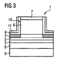
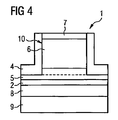
- 当該放射放出半導体チップ(1)は、ウェブ(10)を有するストライプレーザであり、
前記パターニング領域(3)は前記ウェブ(10)のエッジ面に配置されている、請求項1から6までのいずれか1項記載の放射放出半導体チップ。 - 前記パターンエレメントは当該放射放出半導体チップ(1)の半導体層から形成され、
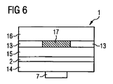
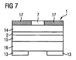
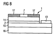
前記媒質は、前記パターンエレメントをカバーするパッシベーション層(4)または吸収層(11)である、請求項7記載の放射放出半導体チップ。 - 当該放射放出半導体チップ(1)は誘電体ミラー(17)を有し、
前記パターンエレメントは前記誘電体ミラー(17)の第1の層から形成され、該誘電体ミラー(17)の第2の層によって包囲されている、請求項1または請求項3から6までのいずれか1項記載の放射放出半導体チップ。 - 前記活性ゾーン(2)は前記パターニング領域(2)を有し、該パターニング領域(2)は量子井戸構造を形成する、請求項1から3までのいずれか1項記載の放射放出半導体チップ。
- 前記パターンエレメントの各基面の基面幅gは、各パターンエレメントの高さhを上回る、請求項1または2記載の放射放出半導体チップ。
- 当該放射放出半導体チップは発光ダイオードであり、
前記パターニング領域(3)は前記発光ダイオードの出力結合層である、請求項11記載の放射放出半導体チップ。 - 当該放射放出半導体チップ(1)は、ウェブ(10)を有するストライプレーザであり、
前記パターニング領域(3)は散乱光を出力結合するために前記ウェブ(10)に隣接して配置されている、請求項11記載の放射放出半導体チップ。 - 請求項1から13までのいずれか1項記載の放射放出半導体チップ(1)の製造方法において、
中断部を有するマスク層を、パターニングすべき領域(30)上に設け、
前記中断部内で前記パターニングすべき領域(30)をエッチングすることにより、前記マスク層が剥離されて、前記パターンエレメントを有するパターニング領域(3)が形成されることを特徴とする、製造方法。 - 請求項1から13までのいずれか1項記載の放射放出半導体チップ(1)の製造方法において、
マスク材料(19)を、パターニングすべき領域(30)から離隔して配置し、エッチングプロセス中に該マスク材料の少なくとも一部を除去して該パターニングすべき領域(30)に堆積させると同時に、前記パターニングすべき領域(30)をエッチングすることにより、前記パターンエレメントが形成されることを特徴とする、製造方法。
Applications Claiming Priority (3)
| Application Number | Priority Date | Filing Date | Title |
|---|---|---|---|
| DE102007046497 | 2007-09-28 | ||
| DE102007060204.0A DE102007060204B4 (de) | 2007-09-28 | 2007-12-14 | Strahlung emittierender Halbleiterchip |
| PCT/DE2008/001423 WO2009039811A2 (de) | 2007-09-28 | 2008-08-27 | Strahlung emittierender halbleiterchip |
Related Child Applications (1)
| Application Number | Title | Priority Date | Filing Date |
|---|---|---|---|
| JP2013269316A Division JP2014057113A (ja) | 2007-09-28 | 2013-12-26 | 放射放出半導体チップ |
Publications (2)
| Publication Number | Publication Date |
|---|---|
| JP2010541215A true JP2010541215A (ja) | 2010-12-24 |
| JP2010541215A5 JP2010541215A5 (ja) | 2013-06-20 |
Family
ID=40435571
Family Applications (2)
| Application Number | Title | Priority Date | Filing Date |
|---|---|---|---|
| JP2010526146A Pending JP2010541215A (ja) | 2007-09-28 | 2008-08-27 | 放射放出半導体チップ |
| JP2013269316A Pending JP2014057113A (ja) | 2007-09-28 | 2013-12-26 | 放射放出半導体チップ |
Family Applications After (1)
| Application Number | Title | Priority Date | Filing Date |
|---|---|---|---|
| JP2013269316A Pending JP2014057113A (ja) | 2007-09-28 | 2013-12-26 | 放射放出半導体チップ |
Country Status (9)
| Country | Link |
|---|---|
| US (1) | US8340146B2 (ja) |
| EP (2) | EP2193556B1 (ja) |
| JP (2) | JP2010541215A (ja) |
| KR (2) | KR101718271B1 (ja) |
| CN (1) | CN101809772B (ja) |
| DE (2) | DE102007063957B3 (ja) |
| PL (1) | PL2193556T3 (ja) |
| TW (1) | TWI385827B (ja) |
| WO (1) | WO2009039811A2 (ja) |
Families Citing this family (6)
| Publication number | Priority date | Publication date | Assignee | Title |
|---|---|---|---|---|
| DE102011100175B4 (de) | 2011-05-02 | 2021-12-23 | OSRAM Opto Semiconductors Gesellschaft mit beschränkter Haftung | Laserlichtquelle mit einer Stegwellenleiterstruktur und einer Modenfilterstruktur |
| DE102012103549B4 (de) | 2012-04-23 | 2020-06-18 | Osram Opto Semiconductors Gmbh | Halbleiterlaserlichtquelle mit einem kantenemittierenden Halbleiterkörper und Licht streuenden Teilbereich |
| DE102013216527A1 (de) * | 2013-08-21 | 2015-02-26 | Osram Opto Semiconductors Gmbh | Laserbauelement und Verfahren zum Herstellen eines Laserbauelements |
| KR20160034534A (ko) | 2014-09-19 | 2016-03-30 | 삼성전자주식회사 | 반도체 발광 소자 |
| KR101689468B1 (ko) * | 2015-05-19 | 2016-12-26 | 주식회사 솔탑 | 라이다식 운고계 장치 및 라이다식 운고계 장치 구현 방법 |
| DE102016106495A1 (de) * | 2016-04-08 | 2017-10-12 | Osram Opto Semiconductors Gmbh | Halbleiterlaser |
Citations (4)
| Publication number | Priority date | Publication date | Assignee | Title |
|---|---|---|---|---|
| JP2000106454A (ja) * | 1998-07-28 | 2000-04-11 | Interuniv Micro Electronica Centrum Vzw | 高効率で放射線を発するデバイスおよびそのようなデバイスの製造方法 |
| JP2004119768A (ja) * | 2002-09-27 | 2004-04-15 | Nippon Telegr & Teleph Corp <Ntt> | 半導体光素子 |
| JP2005311308A (ja) * | 2004-03-05 | 2005-11-04 | Nichia Chem Ind Ltd | 半導体レーザ素子 |
| JP2007220971A (ja) * | 2006-02-17 | 2007-08-30 | Showa Denko Kk | 発光素子及びその製造方法、並びにランプ |
Family Cites Families (13)
| Publication number | Priority date | Publication date | Assignee | Title |
|---|---|---|---|---|
| JPS61108176A (ja) * | 1984-11-01 | 1986-05-26 | Fuji Electric Co Ltd | 粗面化方法 |
| JP2755357B2 (ja) * | 1991-08-30 | 1998-05-20 | シャープ株式会社 | 半導体レーザ素子 |
| JP3448441B2 (ja) * | 1996-11-29 | 2003-09-22 | 三洋電機株式会社 | 発光装置 |
| JP3356436B2 (ja) | 1997-01-27 | 2002-12-16 | インターナシヨナル・ビジネス・マシーンズ・コーポレーシヨン | レーザ装置 |
| JP3633447B2 (ja) * | 1999-09-29 | 2005-03-30 | 豊田合成株式会社 | Iii族窒化物系化合物半導体素子 |
| US6515305B2 (en) * | 2000-09-18 | 2003-02-04 | Regents Of The University Of Minnesota | Vertical cavity surface emitting laser with single mode confinement |
| EP1492209B1 (en) * | 2003-06-27 | 2008-01-09 | Nichia Corporation | Nitride semiconductor laser device having current blocking layer and method of manufacturing the same |
| TWI330413B (en) * | 2005-01-25 | 2010-09-11 | Epistar Corp | A light-emitting device |
| KR100674836B1 (ko) | 2005-02-28 | 2007-01-26 | 삼성전기주식회사 | 고출력 단일모드 반도체 레이저소자 및 그 제조방법 |
| US20060204865A1 (en) * | 2005-03-08 | 2006-09-14 | Luminus Devices, Inc. | Patterned light-emitting devices |
| JP4852972B2 (ja) * | 2005-10-26 | 2012-01-11 | パナソニック電工株式会社 | 光学部品の製造方法及び発光素子 |
| JP2007134445A (ja) * | 2005-11-09 | 2007-05-31 | Nichia Chem Ind Ltd | 窒化物半導体レーザ素子 |
| DE102006017573A1 (de) * | 2006-04-13 | 2007-10-18 | Osram Opto Semiconductors Gmbh | Optoelektronischer Halbleiterkörper und Verfahren zu dessen Herstellung |
-
2007
- 2007-12-14 DE DE102007063957.2A patent/DE102007063957B3/de active Active
- 2007-12-14 DE DE102007060204.0A patent/DE102007060204B4/de active Active
-
2008
- 2008-08-27 KR KR1020157022923A patent/KR101718271B1/ko active IP Right Grant
- 2008-08-27 US US12/679,832 patent/US8340146B2/en active Active
- 2008-08-27 EP EP08834637.4A patent/EP2193556B1/de active Active
- 2008-08-27 CN CN2008801093260A patent/CN101809772B/zh active Active
- 2008-08-27 JP JP2010526146A patent/JP2010541215A/ja active Pending
- 2008-08-27 WO PCT/DE2008/001423 patent/WO2009039811A2/de active Application Filing
- 2008-08-27 PL PL08834637T patent/PL2193556T3/pl unknown
- 2008-08-27 EP EP17157898.2A patent/EP3206239B1/de active Active
- 2008-08-27 KR KR1020107009391A patent/KR101567613B1/ko active IP Right Grant
- 2008-09-02 TW TW097133529A patent/TWI385827B/zh active
-
2013
- 2013-12-26 JP JP2013269316A patent/JP2014057113A/ja active Pending
Patent Citations (4)
| Publication number | Priority date | Publication date | Assignee | Title |
|---|---|---|---|---|
| JP2000106454A (ja) * | 1998-07-28 | 2000-04-11 | Interuniv Micro Electronica Centrum Vzw | 高効率で放射線を発するデバイスおよびそのようなデバイスの製造方法 |
| JP2004119768A (ja) * | 2002-09-27 | 2004-04-15 | Nippon Telegr & Teleph Corp <Ntt> | 半導体光素子 |
| JP2005311308A (ja) * | 2004-03-05 | 2005-11-04 | Nichia Chem Ind Ltd | 半導体レーザ素子 |
| JP2007220971A (ja) * | 2006-02-17 | 2007-08-30 | Showa Denko Kk | 発光素子及びその製造方法、並びにランプ |
Also Published As
| Publication number | Publication date |
|---|---|
| EP3206239A1 (de) | 2017-08-16 |
| KR101567613B1 (ko) | 2015-11-09 |
| WO2009039811A2 (de) | 2009-04-02 |
| DE102007060204B4 (de) | 2019-02-28 |
| TWI385827B (zh) | 2013-02-11 |
| DE102007063957B3 (de) | 2022-10-27 |
| EP3206239B1 (de) | 2021-06-30 |
| CN101809772A (zh) | 2010-08-18 |
| DE102007060204A1 (de) | 2009-04-16 |
| EP2193556B1 (de) | 2017-07-26 |
| KR20100089833A (ko) | 2010-08-12 |
| CN101809772B (zh) | 2012-09-05 |
| WO2009039811A3 (de) | 2009-09-03 |
| US8340146B2 (en) | 2012-12-25 |
| US20100278203A1 (en) | 2010-11-04 |
| TW200917534A (en) | 2009-04-16 |
| KR101718271B1 (ko) | 2017-03-20 |
| KR20150104637A (ko) | 2015-09-15 |
| PL2193556T3 (pl) | 2017-12-29 |
| EP2193556A2 (de) | 2010-06-09 |
| JP2014057113A (ja) | 2014-03-27 |
Similar Documents
| Publication | Publication Date | Title |
|---|---|---|
| TWI499075B (zh) | 具有光擷取結構的半導體發光裝置 | |
| JP4713190B2 (ja) | 面内発光層を含む半導体発光素子 | |
| US7012279B2 (en) | Photonic crystal light emitting device | |
| JP5379434B2 (ja) | 発光素子用サファイア基板の製造方法 | |
| KR101417541B1 (ko) | 반도체 발광 소자 | |
| TWI390759B (zh) | 製造三族氮化物裝置之方法及使用該方法製造之裝置 | |
| US5793062A (en) | Transparent substrate light emitting diodes with directed light output | |
| JP2014057113A (ja) | 放射放出半導体チップ | |
| US20050230699A1 (en) | Light-emitting device with improved optical efficiency | |
| US8232568B2 (en) | High brightness LED utilizing a roughened active layer and conformal cladding | |
| US20100265979A1 (en) | Horizontal emitting, vertical emitting, beam shaped, distributed feedback (dfb) lasers fabricated by growth over a patterned substrate with multiple overgrowth | |
| JP2015099946A (ja) | Ledおよびledの組立方法 | |
| Xi et al. | Enhanced light extraction in GaInN light-emitting diode with pyramid reflector | |
| KR20070081184A (ko) | 질화물계 반도체 발광소자 및 그 제조방법 | |
| CN1729600A (zh) | 具有自对准半导体平台和接触层的半导体器件和相关器件的制造方法 | |
| JP2000174339A (ja) | GaN系半導体発光素子およびGaN系半導体受光素子 | |
| KR101254817B1 (ko) | 반도체 레이저 다이오드 | |
| US7656919B2 (en) | Semiconductor system having a ring laser fabricated by epitaxial layer overgrowth | |
| TWI697076B (zh) | 發光元件及其製造方法 | |
| JP2006190854A (ja) | 発光ダイオード | |
| KR20090103855A (ko) | 질화물계 반도체 발광소자 및 그 제조방법 |
Legal Events
| Date | Code | Title | Description |
|---|---|---|---|
| RD04 | Notification of resignation of power of attorney |
Free format text: JAPANESE INTERMEDIATE CODE: A7424 Effective date: 20101228 |
|
| A521 | Request for written amendment filed |
Free format text: JAPANESE INTERMEDIATE CODE: A523 Effective date: 20110707 |
|
| A621 | Written request for application examination |
Free format text: JAPANESE INTERMEDIATE CODE: A621 Effective date: 20110707 |
|
| A977 | Report on retrieval |
Free format text: JAPANESE INTERMEDIATE CODE: A971007 Effective date: 20121019 |
|
| A131 | Notification of reasons for refusal |
Free format text: JAPANESE INTERMEDIATE CODE: A131 Effective date: 20121026 |
|
| A601 | Written request for extension of time |
Free format text: JAPANESE INTERMEDIATE CODE: A601 Effective date: 20130123 |
|
| A602 | Written permission of extension of time |
Free format text: JAPANESE INTERMEDIATE CODE: A602 Effective date: 20130130 |
|
| A601 | Written request for extension of time |
Free format text: JAPANESE INTERMEDIATE CODE: A601 Effective date: 20130225 |
|
| A602 | Written permission of extension of time |
Free format text: JAPANESE INTERMEDIATE CODE: A602 Effective date: 20130304 |
|
| A524 | Written submission of copy of amendment under article 19 pct |
Free format text: JAPANESE INTERMEDIATE CODE: A524 Effective date: 20130326 |
|
| A02 | Decision of refusal |
Free format text: JAPANESE INTERMEDIATE CODE: A02 Effective date: 20130826 |