JP2010534935A - Method and apparatus for cleaning a substrate surface - Google Patents
Method and apparatus for cleaning a substrate surface Download PDFInfo
- Publication number
- JP2010534935A JP2010534935A JP2010518270A JP2010518270A JP2010534935A JP 2010534935 A JP2010534935 A JP 2010534935A JP 2010518270 A JP2010518270 A JP 2010518270A JP 2010518270 A JP2010518270 A JP 2010518270A JP 2010534935 A JP2010534935 A JP 2010534935A
- Authority
- JP
- Japan
- Prior art keywords
- substrate
- chamber
- gas
- plasma
- processing region
- Prior art date
- Legal status (The legal status is an assumption and is not a legal conclusion. Google has not performed a legal analysis and makes no representation as to the accuracy of the status listed.)
- Pending
Links
Images


Classifications
-
- H—ELECTRICITY
- H01—ELECTRIC ELEMENTS
- H01L—SEMICONDUCTOR DEVICES NOT COVERED BY CLASS H10
- H01L21/00—Processes or apparatus adapted for the manufacture or treatment of semiconductor or solid state devices or of parts thereof
- H01L21/67—Apparatus specially adapted for handling semiconductor or electric solid state devices during manufacture or treatment thereof; Apparatus specially adapted for handling wafers during manufacture or treatment of semiconductor or electric solid state devices or components ; Apparatus not specifically provided for elsewhere
- H01L21/67005—Apparatus not specifically provided for elsewhere
- H01L21/67011—Apparatus for manufacture or treatment
- H01L21/67017—Apparatus for fluid treatment
-
- H—ELECTRICITY
- H01—ELECTRIC ELEMENTS
- H01L—SEMICONDUCTOR DEVICES NOT COVERED BY CLASS H10
- H01L21/00—Processes or apparatus adapted for the manufacture or treatment of semiconductor or solid state devices or of parts thereof
- H01L21/02—Manufacture or treatment of semiconductor devices or of parts thereof
- H01L21/04—Manufacture or treatment of semiconductor devices or of parts thereof the devices having at least one potential-jump barrier or surface barrier, e.g. PN junction, depletion layer or carrier concentration layer
- H01L21/18—Manufacture or treatment of semiconductor devices or of parts thereof the devices having at least one potential-jump barrier or surface barrier, e.g. PN junction, depletion layer or carrier concentration layer the devices having semiconductor bodies comprising elements of Group IV of the Periodic System or AIIIBV compounds with or without impurities, e.g. doping materials
- H01L21/20—Deposition of semiconductor materials on a substrate, e.g. epitaxial growth solid phase epitaxy
-
- C—CHEMISTRY; METALLURGY
- C30—CRYSTAL GROWTH
- C30B—SINGLE-CRYSTAL GROWTH; UNIDIRECTIONAL SOLIDIFICATION OF EUTECTIC MATERIAL OR UNIDIRECTIONAL DEMIXING OF EUTECTOID MATERIAL; REFINING BY ZONE-MELTING OF MATERIAL; PRODUCTION OF A HOMOGENEOUS POLYCRYSTALLINE MATERIAL WITH DEFINED STRUCTURE; SINGLE CRYSTALS OR HOMOGENEOUS POLYCRYSTALLINE MATERIAL WITH DEFINED STRUCTURE; AFTER-TREATMENT OF SINGLE CRYSTALS OR A HOMOGENEOUS POLYCRYSTALLINE MATERIAL WITH DEFINED STRUCTURE; APPARATUS THEREFOR
- C30B25/00—Single-crystal growth by chemical reaction of reactive gases, e.g. chemical vapour-deposition growth
- C30B25/02—Epitaxial-layer growth
- C30B25/08—Reaction chambers; Selection of materials therefor
-
- C—CHEMISTRY; METALLURGY
- C30—CRYSTAL GROWTH
- C30B—SINGLE-CRYSTAL GROWTH; UNIDIRECTIONAL SOLIDIFICATION OF EUTECTIC MATERIAL OR UNIDIRECTIONAL DEMIXING OF EUTECTOID MATERIAL; REFINING BY ZONE-MELTING OF MATERIAL; PRODUCTION OF A HOMOGENEOUS POLYCRYSTALLINE MATERIAL WITH DEFINED STRUCTURE; SINGLE CRYSTALS OR HOMOGENEOUS POLYCRYSTALLINE MATERIAL WITH DEFINED STRUCTURE; AFTER-TREATMENT OF SINGLE CRYSTALS OR A HOMOGENEOUS POLYCRYSTALLINE MATERIAL WITH DEFINED STRUCTURE; APPARATUS THEREFOR
- C30B29/00—Single crystals or homogeneous polycrystalline material with defined structure characterised by the material or by their shape
- C30B29/02—Elements
- C30B29/06—Silicon
-
- H—ELECTRICITY
- H01—ELECTRIC ELEMENTS
- H01L—SEMICONDUCTOR DEVICES NOT COVERED BY CLASS H10
- H01L21/00—Processes or apparatus adapted for the manufacture or treatment of semiconductor or solid state devices or of parts thereof
- H01L21/02—Manufacture or treatment of semiconductor devices or of parts thereof
- H01L21/02041—Cleaning
- H01L21/02043—Cleaning before device manufacture, i.e. Begin-Of-Line process
- H01L21/02046—Dry cleaning only
-
- H—ELECTRICITY
- H01—ELECTRIC ELEMENTS
- H01L—SEMICONDUCTOR DEVICES NOT COVERED BY CLASS H10
- H01L21/00—Processes or apparatus adapted for the manufacture or treatment of semiconductor or solid state devices or of parts thereof
- H01L21/02—Manufacture or treatment of semiconductor devices or of parts thereof
- H01L21/02104—Forming layers
- H01L21/02107—Forming insulating materials on a substrate
- H01L21/02225—Forming insulating materials on a substrate characterised by the process for the formation of the insulating layer
- H01L21/02227—Forming insulating materials on a substrate characterised by the process for the formation of the insulating layer formation by a process other than a deposition process
- H01L21/0223—Forming insulating materials on a substrate characterised by the process for the formation of the insulating layer formation by a process other than a deposition process formation by oxidation, e.g. oxidation of the substrate
- H01L21/02233—Forming insulating materials on a substrate characterised by the process for the formation of the insulating layer formation by a process other than a deposition process formation by oxidation, e.g. oxidation of the substrate of the semiconductor substrate or a semiconductor layer
- H01L21/02236—Forming insulating materials on a substrate characterised by the process for the formation of the insulating layer formation by a process other than a deposition process formation by oxidation, e.g. oxidation of the substrate of the semiconductor substrate or a semiconductor layer group IV semiconductor
- H01L21/02238—Forming insulating materials on a substrate characterised by the process for the formation of the insulating layer formation by a process other than a deposition process formation by oxidation, e.g. oxidation of the substrate of the semiconductor substrate or a semiconductor layer group IV semiconductor silicon in uncombined form, i.e. pure silicon
-
- H—ELECTRICITY
- H01—ELECTRIC ELEMENTS
- H01L—SEMICONDUCTOR DEVICES NOT COVERED BY CLASS H10
- H01L21/00—Processes or apparatus adapted for the manufacture or treatment of semiconductor or solid state devices or of parts thereof
- H01L21/02—Manufacture or treatment of semiconductor devices or of parts thereof
- H01L21/02104—Forming layers
- H01L21/02107—Forming insulating materials on a substrate
- H01L21/02225—Forming insulating materials on a substrate characterised by the process for the formation of the insulating layer
- H01L21/02227—Forming insulating materials on a substrate characterised by the process for the formation of the insulating layer formation by a process other than a deposition process
- H01L21/02255—Forming insulating materials on a substrate characterised by the process for the formation of the insulating layer formation by a process other than a deposition process formation by thermal treatment
-
- H—ELECTRICITY
- H01—ELECTRIC ELEMENTS
- H01L—SEMICONDUCTOR DEVICES NOT COVERED BY CLASS H10
- H01L21/00—Processes or apparatus adapted for the manufacture or treatment of semiconductor or solid state devices or of parts thereof
- H01L21/02—Manufacture or treatment of semiconductor devices or of parts thereof
- H01L21/04—Manufacture or treatment of semiconductor devices or of parts thereof the devices having at least one potential-jump barrier or surface barrier, e.g. PN junction, depletion layer or carrier concentration layer
- H01L21/18—Manufacture or treatment of semiconductor devices or of parts thereof the devices having at least one potential-jump barrier or surface barrier, e.g. PN junction, depletion layer or carrier concentration layer the devices having semiconductor bodies comprising elements of Group IV of the Periodic System or AIIIBV compounds with or without impurities, e.g. doping materials
- H01L21/30—Treatment of semiconductor bodies using processes or apparatus not provided for in groups H01L21/20 - H01L21/26
- H01L21/31—Treatment of semiconductor bodies using processes or apparatus not provided for in groups H01L21/20 - H01L21/26 to form insulating layers thereon, e.g. for masking or by using photolithographic techniques; After treatment of these layers; Selection of materials for these layers
- H01L21/314—Inorganic layers
- H01L21/316—Inorganic layers composed of oxides or glassy oxides or oxide based glass
- H01L21/3165—Inorganic layers composed of oxides or glassy oxides or oxide based glass formed by oxidation
- H01L21/31654—Inorganic layers composed of oxides or glassy oxides or oxide based glass formed by oxidation of semiconductor materials, e.g. the body itself
- H01L21/31658—Inorganic layers composed of oxides or glassy oxides or oxide based glass formed by oxidation of semiconductor materials, e.g. the body itself by thermal oxidation, e.g. of SiGe
- H01L21/31662—Inorganic layers composed of oxides or glassy oxides or oxide based glass formed by oxidation of semiconductor materials, e.g. the body itself by thermal oxidation, e.g. of SiGe of silicon in uncombined form
-
- H—ELECTRICITY
- H01—ELECTRIC ELEMENTS
- H01L—SEMICONDUCTOR DEVICES NOT COVERED BY CLASS H10
- H01L21/00—Processes or apparatus adapted for the manufacture or treatment of semiconductor or solid state devices or of parts thereof
- H01L21/67—Apparatus specially adapted for handling semiconductor or electric solid state devices during manufacture or treatment thereof; Apparatus specially adapted for handling wafers during manufacture or treatment of semiconductor or electric solid state devices or components ; Apparatus not specifically provided for elsewhere
- H01L21/67005—Apparatus not specifically provided for elsewhere
- H01L21/67011—Apparatus for manufacture or treatment
- H01L21/67017—Apparatus for fluid treatment
- H01L21/67028—Apparatus for fluid treatment for cleaning followed by drying, rinsing, stripping, blasting or the like
-
- H—ELECTRICITY
- H01—ELECTRIC ELEMENTS
- H01L—SEMICONDUCTOR DEVICES NOT COVERED BY CLASS H10
- H01L21/00—Processes or apparatus adapted for the manufacture or treatment of semiconductor or solid state devices or of parts thereof
- H01L21/67—Apparatus specially adapted for handling semiconductor or electric solid state devices during manufacture or treatment thereof; Apparatus specially adapted for handling wafers during manufacture or treatment of semiconductor or electric solid state devices or components ; Apparatus not specifically provided for elsewhere
- H01L21/67005—Apparatus not specifically provided for elsewhere
- H01L21/67011—Apparatus for manufacture or treatment
- H01L21/67017—Apparatus for fluid treatment
- H01L21/67063—Apparatus for fluid treatment for etching
- H01L21/67069—Apparatus for fluid treatment for etching for drying etching
-
- H—ELECTRICITY
- H01—ELECTRIC ELEMENTS
- H01L—SEMICONDUCTOR DEVICES NOT COVERED BY CLASS H10
- H01L21/00—Processes or apparatus adapted for the manufacture or treatment of semiconductor or solid state devices or of parts thereof
- H01L21/02—Manufacture or treatment of semiconductor devices or of parts thereof
- H01L21/02104—Forming layers
- H01L21/02365—Forming inorganic semiconducting materials on a substrate
- H01L21/02518—Deposited layers
- H01L21/02521—Materials
- H01L21/02524—Group 14 semiconducting materials
- H01L21/02532—Silicon, silicon germanium, germanium
-
- H—ELECTRICITY
- H01—ELECTRIC ELEMENTS
- H01L—SEMICONDUCTOR DEVICES NOT COVERED BY CLASS H10
- H01L21/00—Processes or apparatus adapted for the manufacture or treatment of semiconductor or solid state devices or of parts thereof
- H01L21/02—Manufacture or treatment of semiconductor devices or of parts thereof
- H01L21/02104—Forming layers
- H01L21/02365—Forming inorganic semiconducting materials on a substrate
- H01L21/02612—Formation types
- H01L21/02617—Deposition types
- H01L21/0262—Reduction or decomposition of gaseous compounds, e.g. CVD
-
- H—ELECTRICITY
- H01—ELECTRIC ELEMENTS
- H01L—SEMICONDUCTOR DEVICES NOT COVERED BY CLASS H10
- H01L21/00—Processes or apparatus adapted for the manufacture or treatment of semiconductor or solid state devices or of parts thereof
- H01L21/02—Manufacture or treatment of semiconductor devices or of parts thereof
- H01L21/02104—Forming layers
- H01L21/02365—Forming inorganic semiconducting materials on a substrate
- H01L21/02656—Special treatments
- H01L21/02658—Pretreatments
- H01L21/02661—In-situ cleaning
-
- Y—GENERAL TAGGING OF NEW TECHNOLOGICAL DEVELOPMENTS; GENERAL TAGGING OF CROSS-SECTIONAL TECHNOLOGIES SPANNING OVER SEVERAL SECTIONS OF THE IPC; TECHNICAL SUBJECTS COVERED BY FORMER USPC CROSS-REFERENCE ART COLLECTIONS [XRACs] AND DIGESTS
- Y10—TECHNICAL SUBJECTS COVERED BY FORMER USPC
- Y10S—TECHNICAL SUBJECTS COVERED BY FORMER USPC CROSS-REFERENCE ART COLLECTIONS [XRACs] AND DIGESTS
- Y10S438/00—Semiconductor device manufacturing: process
- Y10S438/976—Temporary protective layer
Abstract
本発明は概して、クリーンかつダメージのない表面を半導体基板上に形成するための装置および方法を提供する。本発明の一実施形態は、エピタキシャル層を形成する前にプラズマ洗浄プロセスに基板の表面を暴露するように適合された洗浄チャンバを含有するシステムを提供する。一実施形態において、洗浄プロセスを基板に実施する前に、該洗浄チャンバの内部表面にゲッタリング材料を堆積することによって、該洗浄チャンバで処理された基板の汚染物を減少するための方法が用いられる。一実施形態において、酸化およびエッチングステップが洗浄チャンバにおいて基板に繰り返し実施されて、エピタキシャルを配置可能な基板にクリーンな表面を暴露および生成する。一実施形態において、低エネルギプラズマが該洗浄ステップ時に使用される。
【選択図】 図3The present invention generally provides an apparatus and method for forming a clean and damage free surface on a semiconductor substrate. One embodiment of the present invention provides a system containing a cleaning chamber adapted to expose the surface of a substrate to a plasma cleaning process prior to forming an epitaxial layer. In one embodiment, a method is used to reduce contamination of a substrate processed in the cleaning chamber by depositing gettering material on the internal surface of the cleaning chamber before performing the cleaning process on the substrate. It is done. In one embodiment, the oxidation and etching steps are repeatedly performed on the substrate in a cleaning chamber to expose and create a clean surface on the substrate on which the epitaxial can be placed. In one embodiment, a low energy plasma is used during the cleaning step.
[Selection] Figure 3
Description
発明の分野
[0001]本発明の実施形態は概して、半導体基板を処理するための方法および装置に関する。より具体的には、本発明の実施形態は、シリコン基板の表面を洗浄するための方法および装置に関する。
Field of Invention
[0001] Embodiments of the present invention generally relate to methods and apparatus for processing semiconductor substrates. More specifically, embodiments of the present invention relate to a method and apparatus for cleaning the surface of a silicon substrate.
関連技術の説明
[0002]集積回路がシリコンおよび他の半導体基板に形成されている。単結晶シリコンの場合、基板は、溶融シリコンの浴からインゴットを成長させてから、固化インゴットを複数のウェーハに切り取ることによって作られる。次いでエピタキシャルシリコン層が、ドープまたはアンドープ可能な欠陥のないシリコン層を形成するために、単結晶シリコンウェーハ上に形成されてもよい。トランジスタなどの半導体デバイスは、エピタキシャルシリコン層から製造される。形成されたエピタキシャルシリコンの電気特性は概して、単結晶シリコン基板の特性よりも良好である。
Explanation of related technology
[0002] Integrated circuits are formed on silicon and other semiconductor substrates. In the case of single crystal silicon, the substrate is made by growing an ingot from a bath of molten silicon and then cutting the solidified ingot into multiple wafers. An epitaxial silicon layer may then be formed on the single crystal silicon wafer to form a defect-free silicon layer that can be doped or undoped. Semiconductor devices such as transistors are manufactured from epitaxial silicon layers. The electrical properties of the formed epitaxial silicon are generally better than those of the single crystal silicon substrate.
[0003]単結晶シリコンおよびエピタキシャルシリコン層の表面は、通常の周囲条件に暴露される場合に、汚染に感染しやすい。したがって、基板は、エピタキシャル層の形成などの種々の半導体プロセスを実施する前に、シリコンウェーハ表面に見られる不純物および粒子を除去するために洗浄される必要がある。 [0003] The surfaces of single crystal silicon and epitaxial silicon layers are susceptible to contamination when exposed to normal ambient conditions. Therefore, the substrate needs to be cleaned to remove impurities and particles found on the silicon wafer surface before performing various semiconductor processes such as the formation of an epitaxial layer.
[0004]在来、半導体基板は、ウェット洗浄プロセスや在来のプラズマ洗浄プロセスを使用して洗浄される。しかしながら、ウェット洗浄プロセスは「待ち時間」の問題を有しており、これは、1つのロット内の異なるウェーハごとのアイドル時間の変動によって、ウェーハロットにおけるウェーハ間の変動をもたらす恐れがある。在来のリモートまたはイン・シトゥープラズマ洗浄プロセスは、気相または洗浄プロセス中に形成される不要な種の生成によって、チャンバおよびこのチャンバで処理された基板の汚染に起因して極めて困難である。これらの不要な種は、所望の種の洗浄動作を制限するか、洗浄プロセスに他の複雑な問題を持ち込む。 [0004] Conventionally, semiconductor substrates are cleaned using a wet cleaning process or a conventional plasma cleaning process. However, the wet cleaning process has a “latency” problem, which can result in variations between wafers in a wafer lot due to idle time variations for different wafers within a lot. Conventional remote or in-situ plasma cleaning processes are extremely difficult due to contamination of the chamber and the substrate processed in this chamber by the generation of unwanted species formed during the gas phase or cleaning process . These unwanted species limit the cleaning operation of the desired species or introduce other complex problems into the cleaning process.
[0005]したがって、基板表面を洗浄するための、とりわけ、エピタキシャル堆積プロセスを実施する前に基板表面を洗浄するための方法および装置が必要とされる。 [0005] Accordingly, there is a need for a method and apparatus for cleaning a substrate surface, particularly for cleaning a substrate surface prior to performing an epitaxial deposition process.
[0006]本発明は概して、基板を処理するための装置であって、処理領域を形成する1つ以上の壁と、該処理領域に電磁エネルギを送出するように適合されたプラズマ発生源と、該処理領域にシリコン含有ガスを送出するように適合された第1のガス源と、該処理領域に酸化ガスを送出するように適合された第2のガス源とを備える低エネルギ洗浄チャンバと;エピタキシャル層堆積チャンバと;移送領域と、該低エネルギ洗浄チャンバ内の第1の位置と、該エピタキシャル層堆積チャンバ内の第1の位置との間に基板を移送するように適合されたロボットとを囲む1つ以上の壁を有する移送チャンバとを備える装置を提供する。 [0006] The present invention is generally an apparatus for processing a substrate, wherein one or more walls forming a processing region, a plasma generation source adapted to deliver electromagnetic energy to the processing region, A low energy cleaning chamber comprising a first gas source adapted to deliver a silicon-containing gas to the processing region and a second gas source adapted to deliver an oxidizing gas to the processing region; An epitaxial layer deposition chamber; a transfer region; a robot adapted to transfer a substrate between a first position in the low energy cleaning chamber and a first position in the epitaxial layer deposition chamber; And a transfer chamber having one or more walls surrounding it.
[0007]本発明の実施形態はさらに、処理領域を形成する1つ以上の壁と、該処理領域に電磁エネルギを送出するように適合されたプラズマ発生源と、該処理領域内に位置決めされたシールドであって、該シールドが作られた材料が、シリコン、イットリウム、酸化イットリウム、ゲルマニウム、ホウ素、リンおよびシリコンゲルマニウム化合物からなる群より選択されるシールドと、基板サポート表面、およびRF電源によってバイアスされるように適合されたバイアス電極を有する基板サポートと、該処理領域に酸化ガスを送出するように適合された第1のガス源と、該処理領域に不活性ガスを送出するように適合された第2のガス源と、該処理領域にシリコン含有ガスを送出するように適合された第3のガス源とを備える、低エネルギ洗浄プロセスを実施するための装置を提供する。 [0007] Embodiments of the present invention further include one or more walls forming a processing region, a plasma source adapted to deliver electromagnetic energy to the processing region, and positioned within the processing region A shield, wherein the material from which the shield is made is biased by a shield selected from the group consisting of silicon, yttrium, yttrium oxide, germanium, boron, phosphorus, and silicon germanium compounds, a substrate support surface, and an RF power source. A substrate support having a bias electrode adapted to, a first gas source adapted to deliver an oxidizing gas to the processing region, and adapted to deliver an inert gas to the processing region A low energy cleaning comprising a second gas source and a third gas source adapted to deliver a silicon-containing gas to the processing region It provides an apparatus for carrying out the process.
[0008]本発明の実施形態はさらに、エピタキシャル層を形成するための方法であって、洗浄チャンバの処理領域に位置決めされたチャンバコンポーネントの表面にゲッタリング層を堆積するステップと、該洗浄チャンバの該処理領域内に位置決めされた基板サポート上に基板を位置決めするステップと、該基板サポート上に位置決めされた該基板の表面を酸化するステップと、該基板サポート上に位置決めされた該基板の該酸化表面の少なくとも一部を除去するステップと、該表面を水素含有ガスに暴露することによって該酸化表面の少なくとも一部を除去した後に該基板の該表面をパッシベーションするステップと、該基板を該洗浄チャンバからエピタキシャル層堆積チャンバに移送するステップと、該パッシベーション表面の少なくとも一部にエピタキシャル層を堆積するステップとを備える方法を提供する。 [0008] Embodiments of the present invention further provide a method for forming an epitaxial layer, the method comprising depositing a gettering layer on a surface of a chamber component positioned in a processing region of the cleaning chamber; Positioning a substrate on a substrate support positioned in the processing region; oxidizing a surface of the substrate positioned on the substrate support; and oxidizing the substrate positioned on the substrate support Removing at least a portion of the surface; passivating the surface of the substrate after removing at least a portion of the oxidized surface by exposing the surface to a hydrogen-containing gas; and removing the substrate from the cleaning chamber. Transferring to the epitaxial layer deposition chamber from at least one of the passivation surfaces A method comprising the steps of depositing an epitaxial layer.
[0009]本発明の実施形態はさらに、処理領域を形成する1つ以上の壁であって、該1つ以上の壁のうちの少なくとも1つは、該1つ以上の壁の該少なくとも1つの温度を制御するための熱交換デバイスを含有する壁と、電磁エネルギを該処理領域に送出するように適合されたプラズマ発生源と、該処理領域内に位置決めされたシールドと、基板サポート表面、RF電源によってバイアスされるように適合されたバイアス電極、および該基板サポート表面の温度を制御するための基板サポート熱交換デバイスを有する基板サポートと、該処理領域に酸化ガスを送出するように適合された第1のガス源と、該処理領域にエッチングガスを送出するように適合された第2のガス源とを備える、低エネルギ洗浄プロセスを実施するための装置を提供する。 [0009] Embodiments of the present invention further comprise one or more walls forming a processing region, wherein at least one of the one or more walls is the at least one of the one or more walls. A wall containing a heat exchange device for temperature control, a plasma source adapted to deliver electromagnetic energy to the processing region, a shield positioned in the processing region, a substrate support surface, RF A substrate support having a bias electrode adapted to be biased by a power source and a substrate support heat exchange device for controlling the temperature of the substrate support surface, and adapted to deliver an oxidizing gas to the processing region Provided is an apparatus for performing a low energy cleaning process comprising a first gas source and a second gas source adapted to deliver an etching gas to the processing region.
[0010]本発明の上記に引用された特徴が詳細に理解されるように、上記で簡潔に要約された本発明のより具体的な説明が実施形態を参照してなされてもよく、この一部は添付の図面に例示されている。しかしながら、添付の図面は本発明の通常の実施形態のみを例示しており、また、本発明は他の等しく効果的な実施形態を許容可能であるため、この範囲を制限するものとはみなされるべきではない点に留意されたい。
[0017]理解を容易にするために、図面に共通の同一要素を示すのに、可能な場合は同一の参照符号が使用されている。一実施形態に開示されている要素は、特に記載なく他の実施形態に利用されてもよいことが想定されている。 [0017] To facilitate understanding, identical reference numerals have been used, where possible, to designate identical elements that are common to the figures. It is envisioned that elements disclosed in one embodiment may be utilized in other embodiments without specific description.
[0018]本発明は概して、半導体基板(またはウェーハ)上にクリーンかつダメージのない表面を形成するための装置および方法を提供する。本発明の一実施形態は、エピタキシャル層を形成する前に、プラズマ洗浄プロセスに基板表面を暴露するように適合された洗浄チャンバを含有するシステムを提供する。一実施形態において、洗浄プロセスを基板に実施する前に洗浄チャンバの内部表面にゲッタリング材料を堆積することによって、洗浄チャンバで処理された基板の汚染物を減少するための方法が用いられる。ゲッタリング材料は、洗浄チャンバで見られる汚染物を捕捉するものであるため、処理済み基板がクリーンであることを保証することができ、また後にチャンバで処理された基板は同じ所望の洗浄結果を有することになる。一実施形態において、酸化およびエッチングステップは、上部にエピタキシャル膜を有することができる基板にクリーンな表面を暴露または生成するために、洗浄チャンバで基板に対して繰り返し実施される。一実施形態において、低エネルギプラズマがエッチングステップ中に使用される。低エネルギのプラズマは、基板のRFバイアス電力を低下させ、基板全体に印加されるバイアス電位を調整し、処理チャンバでプラズマを発生させるのに使用されるRF電力をパルスにし、基板のRFバイアス電力をパルスにし、軽量な原子種を含有するプラズマを形成し、プラズマを閉じ込めるためにプラズマシールドを使用し、プラズマに対する基板の処理位置を調整することによって、かつ/またはこれらの組み合わせによって達成されてもよい。 [0018] The present invention generally provides an apparatus and method for forming a clean and damage free surface on a semiconductor substrate (or wafer). One embodiment of the present invention provides a system containing a cleaning chamber adapted to expose a substrate surface to a plasma cleaning process prior to forming an epitaxial layer. In one embodiment, a method is used to reduce contamination of a substrate processed in the cleaning chamber by depositing gettering material on the internal surface of the cleaning chamber prior to performing the cleaning process on the substrate. Since the gettering material captures contaminants found in the cleaning chamber, it can ensure that the processed substrate is clean, and the substrate processed later in the chamber will have the same desired cleaning result. Will have. In one embodiment, the oxidation and etching steps are repeatedly performed on the substrate in a cleaning chamber to expose or create a clean surface on the substrate that can have an epitaxial film thereon. In one embodiment, a low energy plasma is used during the etching step. The low energy plasma reduces the RF bias power of the substrate, adjusts the bias potential applied across the substrate, pulses the RF power used to generate the plasma in the processing chamber, and the substrate RF bias power. Can be achieved by forming a plasma containing light atomic species, using a plasma shield to confine the plasma, adjusting the processing position of the substrate relative to the plasma, and / or combinations thereof Good.
洗浄チャンバ
[0019]図1は、本発明の一実施形態にしたがった洗浄チャンバ100の側断面図を概略的に例示している。洗浄チャンバ100は、処理領域122において基板102を洗浄可能な誘導結合プラズマ処理チャンバである。一実施形態において、洗浄チャンバ100は、誘導結合無線周波数(RF)源を使用する、Applied Materials of Santa Claraから入手可能な改良型減結合プラズマ窒化(DPN)チャンバである。DPNチャンバについての詳細な説明は、本明細書に説明されているプロセスのうちの1つ以上を実施するように適合されてもよく、「Plasma Method and Apparatus for Processing a Substrate」と題された米国特許第6,660,659号、および「Method for improving nitrogen profile in plasma nitrided gate dielectric layers」と題された米国特許第7,122,454号に見られ、両者とも参照により本明細書に組み入れられる。
Cleaning chamber
[0019] FIG. 1 schematically illustrates a cross-sectional side view of a
[0020]洗浄チャンバ100は概して、RF源アセンブリ191と、処理チャンバアセンブリ193と、基板サポートアセンブリ194とを備える。処理チャンバアセンブリ193は概して、処理領域122に真空を形成するために使用される複数のコンポーネントを備え、プラズマプロセスはここで実施可能である。一般的に、処理チャンバアセンブリ193は、処理領域122を密閉するチャンバベース127と、チャンバ壁128とチャンバ蓋129とを備える。処理領域122は、チャンバベース127および/またはチャンバ壁128を介して処理領域122に接続されている真空ポンプ110を使用して所望の真空圧にされることが可能である。概して、チャンバ壁128およびチャンバベース127は、アルミニウムなどの金属や他の適切な材料から形成されてもよい。
[0020] The
[0021]一実施形態において、チャンバ壁128およびチャンバ蓋129は温度制御されてもよい。在来の方法および/または熱交換デバイスが、種々のチャンバコンポーネントを加熱および冷却するために使用されてもよい。例えば、チャンバ壁128およびチャンバ蓋129は、処理チャンバアセンブリ193外に位置決めされた、ランプアレイなどのヒーター(図示せず)によって加熱されてもよい。別の例では、チャンバ壁128およびチャンバ蓋129を冷却するために、冷却ガスが処理チャンバアセンブリ193外で循環されてもよい。別の例では、チャンバ壁128およびチャンバ蓋129に埋め込まれてもよい加熱および/または冷却導管が、温度を制御するための流体加熱/冷却デバイスに接続されてもよい。処理チャンバアセンブリ193の温度を制御するために使用されてもよい方法および装置が、「Method for Controlling the Temperature of the Walls of a Reaction Chamber During Processing」と題された米国特許第6,083,323号に見られ、これは参照により本明細書に組み入れられる。
[0021] In one embodiment,
[0022]一実施形態において、RF源アセンブリ191は、コイル109に接続されているRF発生器108およびRF整合回路108Aを概して含有する誘導タイプRF源である。コイル109はチャンバ蓋129に隣接して位置決めされている。一実施形態において、RF発生器108は、約400kHz〜約60MHzの周波数で約0〜約3000Wで動作してもよい。一例において、RF発生器108は13.56MHzの周波数で動作する。一実施形態において、RF発生器108は、低エネルギレベルおよび/またはプラズマ密度を有するプラズマを発生させるために、RFエネルギのパルスをコイル109に提供してもよい。
[0022] In one embodiment, the
[0023]チャンバ蓋129は概して、誘導RF源アセンブリ191から送出されたRFエネルギによって処理領域122にプラズマを形成可能になっている誘電コンポーネント(例えば、石英、セラミック材料(例えばアルミナ))である。
[0023] The
[0024]一実施形態において、処理チャンバアセンブリ193はまた、チャンバベース127と、チャンバ壁128とチャンバ蓋129とによって画成されている処理領域122に1つ以上のプロセスガスを送出するように適合されたガス送出システム150を含有する。一実施形態において、処理領域122は、発生したプラズマと、チャンバで実施された準備プロセスとからチャンバ壁128および/またはチャンバ蓋129を保護するための1つ以上のシールド130によって囲まれている。一実施形態において、ガス送出システム150は、高濃度オゾン(O3)を含有するガスのストリームを発生させるように構成されているオゾン発生器を備える。一実施形態において、ガス送出システムは、ごく少数を列挙するが、シリコン含有ガス(例えば、シラン)、水素含有ガス(例えば、H2)、ゲルマニウム含有ガス、塩素含有ガス、酸素含有ガス(例えば、O2)、三フッ化窒素(NF3)、ホウ素含有ガス(例えば、ジボラン)、および/またはリン含有ガス(例えば、ホスフィン)などの反応ガスを送出するように適合される。一実施形態において、ガス送出システムは、アルゴン(Ar)、ヘリウム(He)、クリプトン(Kr)および/または窒素(N2)などの不活性ガスを送出するように適合される。処理チャンバ122の圧力は、ガス送出システム150によって送出されたガスの流量と、真空ポンプ110のポンピングスピードを調整することによって制御可能である。スロットルバルブ111が、真空ポンプ110のポンピングスピードを調整するために使用されてもよい。
[0024] In one embodiment, the
[0025]基板サポートアセンブリ194は概して、基板サポート部材162Aを含有する基板サポート162を含む。基板サポート部材162Aは、処理中に基板をアクティブに保持するために使用可能な在来の静電チャックであってもよく、あるいは簡素な基板サポートを備えてもよい。温度コントローラ161は概して、温度コントローラ161と、在来の熱交換器(図示せず)に結合された埋め込み型抵抗加熱要素や流体冷却チャネルなどの熱交換デバイスとを使用して基板サポート部材162Aを所望の温度に加熱および/または冷却するように適合される。一実施形態において、温度コントローラ161は、動作し、かつ基板サポート部材162A上に位置決めされた基板102を約20℃〜約800℃の温度に加熱するように適合される。
[0025] The
[0026]処理中、基板サポート162はRF発生器123に接続されてもよいため、処理領域122に形成されたプラズマに存在するイオンを基板102の表面に引き付けるために、RFバイアスが基板サポート162の一部に配置された導電要素に印加可能である。一実施形態において、RF発生器123は、基板洗浄プロセスのうちの1つ以上の部分で基板に陰極または陽極バイアスを発生させて、基板上の保有電荷を調整し、かつ/または基板表面のイオンおよびプラズマ衝突量を制御するように適合される。一実施形態において、基板サポート部材162Aは接地されるかDC(直流)バイアスされる。別の実施形態において、基板サポート部材162Aおよび基板は、基板102のイオン衝突ダメージを最小化するために、プラズマプロセス時には電気的に浮遊している。
[0026] During processing, the
[0027]図1を参照すると、RF発生器108から処理領域122へのRFエネルギの送出によって処理領域122のガス原子はイオン化される。洗浄プロセス中に処理領域122で発生されたプラズマに基板が暴露されると、基板102の表面上の汚染物は、基板102の表面に当たるプラズマのイオン化原子によって移送されたエネルギゆえに、表面から払い落されるか離脱されることがある。一実施形態において、プラズマのイオン化ガス原子は、基板サポート部材162Aを介して基板102に印加されたバイアスゆえに、基板102の表面に引き付けられることもある。
[0027] Referring to FIG. 1, the delivery of RF energy from the
[0028]一実施形態において、RF発生器108によってコイル109に送出されたRF電力は、低エネルギプラズマを形成するためにパルスされる。一実施形態において、パルスされたプラズマプロセスは概して、RF発生器108によってコイル109を使用することによって、時間の関数として処理領域122に送出された一連のシーケンシャルエネルギパルスである。処理領域122に形成されたプラズマを励起するために誘導RF源をパルスすることは、在来のプラズマ処理チャンバで共通して形成されたプラズマ電位ゆえに基板の表面にもたらされたダメージ量を最小化することになる。洗浄プロセスによって基板表面にもたらされたダメージを最小化または排除する必要性は、エピタキシャル層を形成するために準備された単結晶基板にとって重要である。基板表面へのダメージは、形成されたエピタキシャル層における欠陥およびストレスの数を減少するために、最小化される必要がある。したがって、誘導RF源電力をパルスすることによって、低電子温度および低イオンエネルギプラズマを生成および持続させることができる。概して、パルスRF誘導プラズマによって発生されたイオンは、低イオンエネルギ(例えば、<10eV)でイオンを生成し、プラズマ内に位置決めされた基板にダメージを与えることはない。本明細書に説明されている実施形態のうちの1つ以上を享受可能なRF電力のパルス方法の一例は、2003年6月12日に出願された、共に譲渡された米国特許第6,831,021号でさらに論じられており、これは参照により本明細書に組み入れられる。
[0028] In one embodiment, the RF power delivered to the
[0029]図2Aは、本発明の別の実施形態にしたがった洗浄チャンバ100aの側断面図を概略的に例示している。洗浄チャンバ100aは容量結合プラズマチャンバである。洗浄チャンバ100aは、処理チャンバアセンブリ196に結合され、かつ処理領域133を画成するチャンバ蓋129を備える。この構成において、チャンバ蓋アセンブリ130は、(シャワーヘッドとしても知られている)ガス分配プレート132と、ガス分配プレート132に略平行なブロッカープレート134を有するベースプレート131とを備える。ガス分配プレート132は、電気絶縁体135を使用してチャンバ壁128から分離されている。チャンバ蓋アセンブリ130はガス送出アセンブリ150に接続されている。ガス送出システム150からの反応および/または洗浄ガスは、ガス通路136を介して処理領域133に流されてもよい。RF源アセンブリ191は、RF電源を提供してプラズマを発生させるベースプレート131に結合されている。容量プラズマ発生のためのRF源は概して、無線周波数(RF)電源、例えば13.56MHzのRF発生器を備える。処理中、基板サポート部材162Aは接地されてもよい。基板サポート部材162Aとベースプレート131間のバイアス電位は、処理領域133でプラズマに着火してもよい。プラズマの活性種は、基板102を処理するために使用可能である。処理中、基板サポート162AはRF発生器123に接続されてもよいため、処理領域122で発生されたプラズマに存在するイオンを基板102の表面に引き付けるために、基板サポート部材162Aの複数の部分に配置されている導電要素にRFバイアスが印加可能である。容量結合プラズマ反応器についてのより詳細な説明は、「Apparatus for distributing gases in a chemical vapor deposition system」と題された米国特許第6,495,233号に見ることができ、これは参照により本明細書に組み入れられる。
[0029] FIG. 2A schematically illustrates a cross-sectional side view of a
[0030]上記の洗浄チャンバ100および100a(図1および2)は、半導体基板を洗浄するために使用されてもよい。特に、本発明の洗浄チャンバ100および100aは、ダメージのない洗浄をシリコン表面に実施するために使用されてもよい。
[0030] The
[0031]別の実施形態において、洗浄チャンバは、ここに説明されている洗浄プロセスを実施するために使用されるプラズマを発生させるために、マイクロ波エネルギ源(図示せず)を使用してもよい。 [0031] In another embodiment, the cleaning chamber may use a microwave energy source (not shown) to generate a plasma that is used to perform the cleaning process described herein. Good.
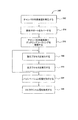
基板表面の洗浄方法
[0032]図3は、本発明の一実施形態にしたがった、半導体基板の洗浄方法200のフローチャートを例示している。一実施形態において、方法200は、上記の洗浄チャンバ100または100aで実施されてもよい。一実施形態において、洗浄プロセスは概して、プラズマ洗浄プロセスを使用して、クリーンかつダメージのない表面を半導体基板上に形成する方法を提供する。
Substrate surface cleaning method
[0032] FIG. 3 illustrates a flowchart of a
[0033]ステップ212において、洗浄チャンバ100や洗浄チャンバ100aなどの洗浄チャンバの内部表面が再生されてもよい。一実施形態において、ステップ212は、洗浄チャンバの種々の内側表面に見られる不要な残渣材料および/または汚染物を除去するためのエッチングプロセスを行うことを備える。在来のスパッタエッチングおよび/または化学支援エッチングプロセスが、チャンバ壁やシールド130などの洗浄チャンバの内部表面を再生するために実施されてもよい。
[0033] In
[0034]一実施形態において、反応ガスのリモートまたはイン・シトゥ−プラズマが、洗浄チャンバの内部表面の汚染物を除去するために使用されてもよい。反応ガスは、共通して使用されているハロゲンおよびハロゲン化合物を含む広範囲のガスから選択されてもよい。例えば、反応ガスは、除去される堆積材料に応じて、三フッ化窒素(NF3)、四フッ化炭素(CF4)、六フッ化硫黄(SF6)、ヘキサフルオロエタン(C2F6)、四塩化炭素(CCl4)、ヘキサクロロエタン(C2Cl6)またはこれらの組み合わせなどの塩化物、フッ化物またはこれらの化合物であってもよい。 [0034] In one embodiment, a remote or in-situ plasma of the reactive gas may be used to remove contaminants on the interior surface of the cleaning chamber. The reaction gas may be selected from a wide range of gases including commonly used halogens and halogen compounds. For example, the reactive gas may be nitrogen trifluoride (NF 3 ), carbon tetrafluoride (CF 4 ), sulfur hexafluoride (SF 6 ), hexafluoroethane (C 2 F 6 ) depending on the deposition material to be removed. ), Carbon tetrachloride (CCl 4 ), hexachloroethane (C 2 Cl 6 ), or combinations thereof, fluorides or compounds thereof.
[0035]一実施形態において、アルゴン、窒素、ヘリウム、水素または酸素などのキャリアガスが、不要な種を除去し、かつ/またはエッチングプロセスを支援したり、洗浄チャンバにおけるプラズマの初期化および/または安定化の助けとなるように、洗浄チャンバの処理領域に送出されてもよい。 [0035] In one embodiment, a carrier gas, such as argon, nitrogen, helium, hydrogen or oxygen, removes unwanted species and / or assists in the etching process, initializes the plasma in the cleaning chamber, and / or It may be delivered to the processing area of the cleaning chamber to aid in stabilization.
[0036]一実施形態において、洗浄ガスが、洗浄チャンバの内部表面の、シリコン(Si)などの(後述の)ゲッタリング材料を含むコーティングをエッチングするために洗浄チャンバに送出されてもよい。洗浄ガスは、加熱された三フッ化窒素(NF3)、塩化水素(HCl)またはこれらの組み合わせを含んでもよい。一実施形態において、在来のリモートプラズマ源(RPS)は、処理チャンバの処理領域に結合されてもよい。RPSは概して、真空ポンプ110によって空にされているチャンバコンポーネントから堆積物や他のプロセス副生成物を除去する、解離(Disassociated)フッ素などの反応性洗浄剤を提供する。
[0036] In one embodiment, a cleaning gas may be delivered to the cleaning chamber to etch a coating that includes a gettering material (described below), such as silicon (Si), on the inner surface of the cleaning chamber. The cleaning gas may include heated nitrogen trifluoride (NF 3 ), hydrogen chloride (HCl), or combinations thereof. In one embodiment, a conventional remote plasma source (RPS) may be coupled to the processing region of the processing chamber. RPS generally provides a reactive cleaning agent, such as dissociated fluorine, that removes deposits and other process by-products from the chamber components evacuated by
[0037]ステップ214において、シャッターディスクまたはダミー基板が、図1および2Aの基板サポート部材162Aなどの基板サポート部材の上部表面をカバーするために使用されてもよい。シャッターディスクまたはダミー基板は、ステップ216などの後続の堆積時に基板サポート部材への堆積を防止するために使用され、処理中の基板は、洗浄チャンバ内に形成されたコーティングとは接触しない。基板サポート部材をカバーすることはまた、基板サポート部材が、処理中に基板を保持するように構成されている静電チャックである場合には、チャックに関する問題を回避することも可能である。
[0037] In
[0038]ステップ216において、一実施形態において、チャンバ壁128、シールド130、シャワーリング138、チャンバ蓋129などの洗浄チャンバコンポーネントのうちの1つ以上が、ゲッタリングコーティングをこの上に堆積することによって調節されてもよい。ゲッタリングコーティングは1つ以上のゲッタリング材料を含んでもよい。ゲッタリング材料という用語は概して、洗浄プロセス前またはこの最中に洗浄チャンバに見られる不純物を固定化および/または吸収(つまり、物理吸収または化学吸収)するために使用される任意の材料のことをいう。ゲッタリング材料は、洗浄チャンバにおける不要な副生成物を除去するように選択される一方で、新たな副生成物の発生、粒子の発生、RF電力の不要な消耗、または処理領域122に見られる所望の種の除去などの厄介な問題を提示することはない。ステップ216で形成された堆積ゲッタリングコーティングの厚さは約10A〜約1μmであってもよい。内部表面のコーティングは、引き続き処理された基板の汚染物を減少または防止するために使用されてもよい。コーティングは、純シリコン材料(例えば、エピタキシャルSi層、多結晶Si層、アモルファスSi層)、シリコン含有層、ゲルマニウム含有層、および/または、所望のレベルの1つ以上の共通ドーパント材料(例えば、ホウ素(B)、リン(P))を含有するシリコンまたはゲルマニウム層、あるいはこれらの組み合わせを含んでもよい。純シリコンから形成されるコーティングは、エピタキシャル層をこの上に形成するシリコン基板に共通してみられる多くの汚染物に対して強力なゲッタリング作用を有すると考えられている。シリコンの使用はまた、金属汚染物や、基板の洗浄済み表面に後に形成されたエピタキシャル層の位置決めによってもたらされるデバイス歩留まりに対する粒子汚染の効果を最小化するのに有用である。一例では、ゲッタリングコーティングは、処理チャンバの処理領域に送出されたシラン(SiH4)含有ガスを使用して、約0.1〜約5.0トールの圧力、および約200ワット〜約2kWのRF電力に堆積されるのに対して、チャンバコンポーネントの温度は約200℃〜約500℃の範囲に維持される。
[0038] At
[0039]一実施形態において、酸素をゲッタリングするように構成されているゲッタリング材料の層が、洗浄チャンバの内部表面に堆積されてもよい。一実施形態において、コーティングは、約10A〜約1μmの厚さのシリコン(Si)層を備える。シリコンコーティングは、チャンバの処理領域に位置決めされた加熱済みコンポーネントにシリコン含有前駆体を送出する通常のCVDまたはALDタイププロセスを使用して堆積されてもよい。ゲッタリング材料を受け取るコンポーネントは、外部ランプや埋め込み型抵抗加熱要素を使用して加熱されてもよく、かつ/またはRFプラズマを使用して加熱されてもよい。 [0039] In one embodiment, a layer of gettering material configured to getter oxygen may be deposited on the interior surface of the cleaning chamber. In one embodiment, the coating comprises a silicon (Si) layer that is about 10 A to about 1 μm thick. The silicon coating may be deposited using a conventional CVD or ALD type process that delivers a silicon-containing precursor to a heated component positioned in the processing region of the chamber. The component that receives the gettering material may be heated using an external lamp, an embedded resistive heating element, and / or may be heated using an RF plasma.
[0040]ステップ216で堆積されたゲッタリング材料のコーティングは、洗浄プロセス時に生成された望ましくない種を固定化、吸収または吸着することができる。結果として、コーティングのゲッタリング能力は、アクティブ表面がカバーされるか、反応性が小さくなると低下する。この問題を補償するために、ゲッタリング材料の新たなコーティングが、ステップ212、214、216を繰り返すことによって処理領域122のコンポーネントに形成されてもよい。一実施形態において、ステップ212、214、216は、洗浄チャンバで各基板を処理する前に繰り返されてもよい。別の実施形態において、ステップ212、214、216は、洗浄チャンバで複数の基板を処理した後に繰り返されてもよい。
[0040] The coating of gettering material deposited in
[0041]ゲッタリング材料の層を堆積した後、シャッターディスク、ダミーディスクまたはダミー基板は洗浄チャンバから除去される。次に、洗浄される基板が洗浄チャンバに配置される。洗浄チャンバは概して真空状態に保たれるため、酸素、炭素、フッ素、シリコンおよび塩素などの、基板表面に見られる汚染物および粒子は離脱または除去されてもよく、洗浄チャンバの内部表面に形成されたコーティングによってゲッタリングされることが可能である。 [0041] After depositing the layer of gettering material, the shutter disk, dummy disk or dummy substrate is removed from the cleaning chamber. Next, the substrate to be cleaned is placed in a cleaning chamber. Since the cleaning chamber is generally kept in a vacuum, contaminants and particles found on the substrate surface, such as oxygen, carbon, fluorine, silicon and chlorine, may be detached or removed and formed on the inner surface of the cleaning chamber. It can be gettered by a different coating.
[0042]基板は次いで、後述される1つ以上の酸化およびエッチングステップを実施することによって洗浄される。酸化プロセスは、基板の表面に見られる、汚染され、またはダメージを受けたシリコンを消費するために使用される。形成された酸化層は次いで、新たなクリーンなシリコン表面を暴露するために除去される。酸化プロセスはステップ220で説明されており、エッチングステップはステップ222で説明されている。
[0042] The substrate is then cleaned by performing one or more oxidation and etching steps described below. The oxidation process is used to consume contaminated or damaged silicon found on the surface of the substrate. The formed oxide layer is then removed to expose a new clean silicon surface. The oxidation process is described at
[0043]ステップ220において、酸化剤が、洗浄中の基板の上部層に酸化物を発生させるために洗浄チャンバに送出される。一実施形態において、酸化剤はオゾン(O3)を含んでおり、これは、比較的低い温度でシリコンの酸化を可能にする。一実施形態において、オゾンは、プラズマ、紫外線(UV)エネルギ、またはプラズマおよびUVエネルギの組み合わせに酸素を暴露することによって、オゾン発生器で発生されてもよい。一実施形態において、UVランプ145が、処理中に基板の表面にエネルギを送出するように位置決めされている。一実施形態(図示せず)では、UVランプは、チャンバ壁128のうちの1つに形成されたポートを介してUV光を送出できるように位置決めされている。酸化方法についての詳細な説明は、「Thermally Oxidizing Silicon Using Ozone」と題された米国特許出願公開第2006/0223315号と、「Method and a System For Sealing An Epitaxial Silicon Layer On A Substrate」と題された米国特許出願公開第2002/0115266号に見ることができ、両者とも参照により本明細書に組み入れられる。
[0043] In
[0044]一実施形態において、基板表面は、高温酸化プロセスを使用して酸化される。この場合、基板は、図1の基板サポート部材162Aなどの基板サポート部材で、約400℃〜約700℃の温度に加熱されてもよい。酸化時に、洗浄チャンバは、基板より低い温度に維持される。例えば、ガス分配経路を含む洗浄チャンバコンポーネント(例えば、壁、シールド)は、400℃未満、つまり400℃より実質的に低い温度に維持される。一実施形態において、基板サポート部材/ヒーターは約700℃に維持され、洗浄チャンバは約350℃に維持される。一実施形態において、壁は、処理チャンバの壁に形成されたチャネルを流れる流体を使用して温度制御される。
[0044] In one embodiment, the substrate surface is oxidized using a high temperature oxidation process. In this case, the substrate may be heated to a temperature of about 400 ° C. to about 700 ° C. with a substrate support member, such as the
[0045]ステップ222において、次いでエッチングプロセスが、ステップ220で形成された酸化物を除去するために実施される。エッチングプロセスは、物理的、化学的、あるいは物理的および化学的エッチング技術の組み合わせを使用して達成されてもよい。
[0045] In
[0046]化学的エッチングの場合、エッチングガスが洗浄チャンバに送出されてもよく、プラズマが、基板上で材料と化学反応する反応種を発生させるために着火されてもよい。この反応の揮発性副生成物は、洗浄チャンバに接続された真空システムによって除去され、さらに/またはステップ216でチャンバコンポーネントの表面に形成されたコーティングによってゲッタリングされる。エッチングガスは、塩素、フッ素、または、ステップ220で基板表面に形成された酸化物の除去に適した他の化合物を含んでもよい。一実施形態において、エッチングガスは、三フッ化窒素(NF3)、塩素イオン(Cl)、およびアルゴンなどのキャリアガスを含む。
[0046] In the case of chemical etching, an etching gas may be delivered to the cleaning chamber and the plasma may be ignited to generate reactive species that chemically react with the material on the substrate. Volatile by-products of this reaction are removed by a vacuum system connected to the cleaning chamber and / or gettered by a coating formed on the surface of the chamber component at
[0047]物理的エッチングが、基板表面に衝突して、基板表面から材料を物理的に除去するために使用されるエネルギ種を提供するプラズマを発生させることによって実施される。場合によっては、基板サポートにバイアスを提供して、プラズマに形成されたイオンを基板表面に向かって加速させることが望ましい。衝突イオンは、スパッタエッチング動作によって、基板表面の材料を物理的に除去する。基板表面の低エネルギの物理的衝突は概して、基板表面のシリコン格子へのダメージ量を減少するのに望ましい。低電力バイアスは、酸化層を除去して、基板の表面へのダメージを最小化するために使用されてもよい。在来のドライエッチングプロセスは概して、プラズマ支援材料除去プロセスによって生成された基板材料格子のダメージに関係なく、材料を急速に除去するために使用される。在来のスパッタエッチング技術は概して、衝突イオン/および副生成物の高エネルギゆえに、エピタキシャル堆積ステップを実施する前に基板を洗浄するのには望ましくない。より具体的には、本発明のエッチングプロセスは、ステップ222において基板表面で暴露された結晶性材料へのダメージを最小化するために、エッチングプロセス時に形成されたイオンのエネルギを調整する工程を備える。一実施形態において、ゲッタリング層をこの中に配置しているチャンバにおいて低RF電力の材料除去プロセスを使用することによって、ステップ222で実施された材料除去プロセスは、ダメージのない、かつクリーンな表面を基板に形成することになり、このことは、後続の堆積プロセス時に高品質のエピタキシャル層が形成されることを保証するのに重要である。一実施形態において、RF発生器123は、約25W〜約500Wの平均RFバイアス電力を、基板サポート162に配置された導電要素に送出して、エッチングプロセスを実施するように適合される。
[0047] Physical etching is performed by generating a plasma that impacts the substrate surface and provides the energy species used to physically remove material from the substrate surface. In some cases, it may be desirable to provide a bias to the substrate support to accelerate ions formed in the plasma toward the substrate surface. The collision ions physically remove the material on the substrate surface by a sputter etching operation. Low energy physical collisions of the substrate surface are generally desirable to reduce the amount of damage to the silicon lattice on the substrate surface. A low power bias may be used to remove the oxide layer and minimize damage to the surface of the substrate. Conventional dry etching processes are generally used to rapidly remove material regardless of the damage to the substrate material lattice produced by the plasma assisted material removal process. Conventional sputter etching techniques are generally undesirable for cleaning a substrate prior to performing an epitaxial deposition step because of the high energy of impact ions / and byproducts. More specifically, the etching process of the present invention comprises adjusting the energy of ions formed during the etching process to minimize damage to the crystalline material exposed at the substrate surface in
[0048]方法200の代替実施形態において、ステップ216は、ステップ220の後で、ステップ222を実施する前に実施される。この代替実施形態の一態様では、ステップ220および222は異なるチャンバで実施されるため、ゲッタリング層は、ステップ222を実施する前に、酸化基板の表面には堆積されない(ステップ216)。単一の洗浄チャンバが使用される代替実施形態の別の態様では、ステップ220が基板に実施されてから、基板は洗浄チャンバから除去されるため、ダミー基板は、酸化基板の表面をゲッタリング材料でコーティングすることなくステップ216が実施されるように挿入可能であり、そしてダミー基板は除去されて、酸化基板が保有されるため、ステップ222は実施可能である。
[0048] In an alternative embodiment of
[0049]図4は、物理的エッチングプロセスをもたらしうる機構を概して例示している、洗浄チャンバ300の部分的側断面図を概略的に例示している。洗浄チャンバ300は、処理領域302を画成するチャンバ本体301を有する。洗浄される基板303は、処理領域302において基板サポート304上に配置されてもよい。コイル305が、処理領域302の上部にプラズマ308を発生させるために、チャンバ本体301の上部の外側に位置決めされる。RF源306が、プラズマを発生させるためのRFエネルギを提供するために、コイル305に接続されてもよい。バイアス源307が、基板303および/または基板サポート304にバイアス電位を提供するために、基板サポート304に結合されてもよい。プラズマ308で発生された活性種309またはイオン310は、基板303の上部表面303Aに引き付けられてもよく、この上の材料を除去する。
[0049] FIG. 4 schematically illustrates a partial cross-sectional side view of a
[0050]一実施形態において、活性種309および/またはイオン310のエネルギは、材料の除去中に上部表面303Aに物理的ダメージが生じないように調整されてもよい。この調整は、基板RFバイアス電力を低下させ、基板全体に印加されたバイアス電位を調整し、プラズマ発生コンポーネント(例えば、誘導結合デバイス(例えば、コイル))、容量結合デバイス(例えば、シャワーヘッド、マイクロ波源))に送出されたRF電力をパルスにし、基板のRFバイアス電力をパルスにし、エッチングガスに軽量な原子種を含有するプラズマを形成し、プラズマを閉じ込めるためにプラズマシールドを使用し、プラズマに対する基板の処理位置を調整することによって、かつ/またはこれらの組み合わせによって達成されてもよい。
[0050] In one embodiment, the energy of the
[0051]一実施形態において、活性種のエネルギは、基板サポートに送出された低RFバイアス電力を使用することによって減少されてもよい。一実施形態において、図4のバイアス源307などのバイアス源の電力は、基板の上部表面から二酸化シリコンを除去するために、約50Wに設定されてもよい。
[0051] In one embodiment, the energy of the active species may be reduced by using low RF bias power delivered to the substrate support. In one embodiment, the power of a bias source, such as
[0052]一実施形態において、図4のバイアス源307などのバイアス源の電位は、基板上のバイアスを低下させるために陰極でなくなるように調整されてもよい。一実施形態において、バイアス源は排除されてもよく、また基板は、接地された基板サポートに位置決めされる。別の実施形態において、リバースバイアスが、プラズマにおけるイオンおよび反応性イオン種に反発力を加えるために印加されてもよい。例えば、シリコン・オン・インシュレータ基板を洗浄する場合にリバースバイアスが使用されてもよい。
[0052] In one embodiment, the potential of a bias source, such as
[0053]一実施形態において、プラズマエネルギは、RF源および/または基板バイアス源をパルスすることによって低下されてもよい。エネルギ低下の度合いは、プラズマ発生コンポーネント(例えば、コイル、シャワーヘッド、マイクロ波源)に送出されたRFパルスのデューティサイクルを調整することによって制御されてもよい。RF源をパルスすることによって、RF源によって発生されたプラズマの活性種の密度を低下させる。一実施形態において、洗浄プロセス時に洗浄チャンバに低エネルギプラズマを維持するように、RF源がパルスされる。RF源をパルスすることによって、プラズマ処理領域の全プラズマおよび活性種密度を低下させることによって、衝突する種のエネルギおよび数を減少して、基板へのダメージを回避する。パルスプラズマプロセスに関する詳細な記述は、2007年12月20に出願され、「Method and Apparatus for Fabricating a High Dielectric Constant Transistor Gate Using a Low Energy Plasma Apparatus」と題された米国特許出願第11/614,019号(整理番号第APPM10983号)に見られ、これは参照により本明細書に組み入れられる。 [0053] In one embodiment, the plasma energy may be reduced by pulsing the RF source and / or the substrate bias source. The degree of energy reduction may be controlled by adjusting the duty cycle of the RF pulses delivered to the plasma generating component (eg, coil, showerhead, microwave source). By pulsing the RF source, the density of active species in the plasma generated by the RF source is reduced. In one embodiment, the RF source is pulsed to maintain a low energy plasma in the cleaning chamber during the cleaning process. By pulsing the RF source, the total plasma and active species density in the plasma processing region is reduced, thereby reducing the energy and number of impinging species and avoiding damage to the substrate. A detailed description of the pulsed plasma process was filed on Dec. 20, 2007, entitled “Method and Apparatus for Fabricating a High Dielectric Constant Transistor Gate, US Patent No. 9 / Apr. No. (Docket No. APPM10983), which is incorporated herein by reference.
[0054]一実施形態において、エッチングガスは、低エネルギプラズマを発生させて、物理的エッチングプロセスによって基板表面に生成されたダメージを減少または最小化するために使用される1つ以上のより軽量な種を含む。一実施形態において、ヘリウム(He)、ネオン(Ne)、水素(H2)またはこれらの組み合わせなどのより軽量なガス種が、アルゴン(Ar)などの他のプロセスガスを含有するエッチングガスに添加されてもよい。一実施形態において、エッチングガスはアルゴンおよびヘリウムを含む。別の実施形態において、エッチングガスは、アルゴン、ヘリウムおよび水素ガスを実質的に含む。別の実施形態において、エッチングガスはアルゴンおよび水素を含む。別の実施形態において、エッチングガスはアルゴンおよび窒素を含む。さらに別の実施形態において、エッチングガスは、ヘリウム(He)、ネオン(Ne)または水素(H2)を実質的に含む。 [0054] In one embodiment, the etching gas generates one or more lighter plasmas that are used to generate a low energy plasma to reduce or minimize damage generated on the substrate surface by the physical etching process. Including species. In one embodiment, a lighter gas species such as helium (He), neon (Ne), hydrogen (H 2 ) or combinations thereof is added to an etching gas containing other process gases such as argon (Ar). May be. In one embodiment, the etching gas includes argon and helium. In another embodiment, the etching gas substantially comprises argon, helium and hydrogen gas. In another embodiment, the etching gas includes argon and hydrogen. In another embodiment, the etching gas includes argon and nitrogen. In yet another embodiment, the etching gas substantially comprises helium (He), neon (Ne), or hydrogen (H 2 ).
[0055]別の実施形態において、プラズマシールド140(図2B)は、処理中に基板の表面付近に位置決めされてもよい。図2Bは、プラズマシールド140を含有する洗浄チャンバ100の一実施形態の側断面図を概略的に例示している。プラズマシールドは、基板の表面付近で衝突する種の量および/またはエネルギを減少または最小化するために使用される。プラズマシールド140は、処理中にプラズマおよび/またはプロセスガスの一部を通過させる孔あきまたは多孔性材料であってもよい。一実施形態において、孔は、プラズマシールドを通過する複数のホール141である。一実施形態において、プラズマシールドは誘電材料からなるか、誘電材料でコーティングされ、これはプラズマおよびプロセスガス(例えば、石英、SiO2)と両立する。一実施形態において、プラズマシールドは、チャンバ蓋129やチャンバ壁128が作られる材料などの、チャンバの他のコンポーネントと同じ材料からなる。一実施形態において、プラズマシールドは、シリコン、イットリウム、酸化イットリウム、ゲルマニウム、ホウ素、リンおよびシリコンゲルマニウム化合物からなる群より選択された材料からなる。
[0055] In another embodiment, the plasma shield 140 (FIG. 2B) may be positioned near the surface of the substrate during processing. FIG. 2B schematically illustrates a side cross-sectional view of one embodiment of the
[0056]別の実施形態において、処理中の基板と、洗浄チャンバで発生されたプラズマとの相対的位置は、プラズマにおけるイオンや活性種による基板表面への衝突量を調整するように調整されてもよい。同様の調整は、「Multi−Layer High Quality Gate Dielectric for Low−Temperature Poly−Silicon TFTs」と題された、共に譲渡された米国特許出願公開第2006/0105114号に説明されており、これは参照により本明細書に組み入れられる。 [0056] In another embodiment, the relative position of the substrate being processed and the plasma generated in the cleaning chamber is adjusted to adjust the amount of ions or active species impacting the substrate surface in the plasma. Also good. A similar adjustment is described in co-assigned US Patent Application Publication No. 2006/0105114 entitled “Multi-Layer High Quality Gate Dielectric for Low-Temperature Poly-Silicon TFTs”. It is incorporated herein.
[0057]図3を再度参照すると、ステップ222の例示的エッチングプロセスは、図1の洗浄チャンバ100に類似する洗浄チャンバにおいて、基板の上部表面に形成されたシリコン酸化物を除去するために実施されてもよい。処理中、チャンバ圧力は約1ミリトール〜約1トールに維持されてもよい。一実施形態において、チャンバ圧力は約20ミリトール〜約800ミリトールに維持されてもよい。ヘリウムおよびアルゴンを含むエッチングガスが処理領域に提供されてもよい。一実施形態において、チャンバ圧力は約5ミリトール〜約20ミリトールであってもよく、エッチングガスは主にヘリウムを含む。処理中の基板はまた、最大約700℃の温度に加熱されてもよい。洗浄チャンバは、約20℃〜約400℃の温度に維持されてもよい。一実施形態において、チャンバは約30℃の温度に維持される。チャンバ壁をより低い温度に維持することは、チャンバ壁の腐食を少なくする助けとなりうると思われる。
[0057] Referring back to FIG. 3, the exemplary etching process of
[0058]図3に戻ると、ステップ220、222は、基板が洗浄されるまで、1回以上繰り返されてもよい。基板表面が洗浄されると、ステップ224および/またはステップ226は、クリーンな基板表面に実施されてもよい。
[0058] Returning to FIG. 3,
[0059]ステップ224において、パッシベーション処置は洗浄済み基板に実施されるため、後続のエピタキシャル堆積プロセスまで基板がクリーンなままである。一実施形態において、パッシベーション処置は、パッシベーションガスを流すステップと、パッシベーションガスのプラズマを発生させるステップとを備える。一実施形態において、パッシベーションガスは、洗浄済みシリコン表面を水素で終端するために使用される希釈濃度の水素ガス(H2)を含む。一実施形態において、パッシベーション処置は、約1%の水素ガスを含む水素含有ガスを送出するステップを備えるが、基板は約50〜約500℃の温度に維持される。
[0059] In
[0060]ステップ226において、エピタキシャルシリコン層が、エピタキシャルチャンバにおいて洗浄済み基板上に成長されてもよい。CVDプロセスを使用してシリコンエピタキシャル層を成長させるために、基板は、例えば約500℃〜800℃の高温、かつ低圧力状態または大気圧に設定されたエピタキシャルチャンバに位置決めされる。高温および低圧力状態を維持しつつ、モノシランガスやジクロロシランガスなどのシリコン含有ガスがエピタキシャルチャンバに供給されて、シリコンエピタキシャル層が気相成長によって成長されて、基板と同じ結晶配向を有する半導体層を形成する。プロセスは、約0.1トール〜約760トールの範囲の圧力で動作してもよい。シリコン含有膜を堆積するために使用されてもよいハードウェアは、Santa Clara,CalifにあるApplied Materials,incから入手可能なEpi Centura RTMシステムおよびPoly Gen RTMシステムを含む。エピタキシャルチャンバについての詳細な説明は、「Modular CVD EPI 300mm Reactor」と題され、2007年6月25日に出願された米国特許出願第11/767,619号(整理番号第10394号)に見られ、参照により本明細書に組み入れられる。
[0060] In
[0061]方法200は、洗浄チャンバおよびエピタキシャルチャンバを備えるクラスタツールで実施されてもよい。在来の構成では、基板は、在来の洗浄プロセス(例えば、ウェット洗浄プロセス)を実施した後、エピタキシャル堆積チャンバに移送されてエピタキシャル層を形成するまでの期間待機させられてもよい。待機するプロセスは、基板表面の清浄度に影響する恐れがあり、これはウェーハ間のプロセス結果に影響する恐れがある。一実施形態において、ステップ224の完了と後続のエピタキシャル層堆積プロセス(つまり、ステップ226)との間のタイミングは、パッシベーションプロセスが完了された直後に基板がエピタキシャルチャンバに移送されるようにスケジューリングされる。プロセスタイミング、つまりスケジューリングを制御するコントローラ147の使用は、プロセス反復性およびデバイス歩留まりを改良することができる。一実施形態において、待ちステップが、パッシベーション後の待機を排除するために、ステップ224の前に追加されてもよい。別の実施形態において、ステップ222および/または224が完了されるとエピタキシャル堆積チャンバが基板を受け取る用意ができることをコントローラ147が確認するまで、ステップ222および/またはステップ224は開始されない。
[0061] The
[0062]一実施形態において、ステップ220は第1の洗浄チャンバ100で実施され、ステップ222は第2の洗浄チャンバ100で実施されて、ステップ220がステップ222に対して有する、またはこの反対のプロセス作用を減少させる。一実施形態において、第1の洗浄チャンバ100はステップ212〜220を実施してもよく、第2の洗浄チャンバ100はステップ212〜216およびステップ222〜224を実施してもよい。
[0062] In one embodiment,
[0063]コントローラ147は概して、第1の洗浄チャンバ100およびシステム400(図5)の制御および自動化を容易にするように設計されており、また通常、中央演算処理装置(CPU)(図示せず)と、メモリ(図示せず)と、サポート回路(またはI/O)(図示せず)とを含んでもよい。CPUは、種々のチャンバプロセスおよびハードウェア(例えば、検出器、モータ、流体送出ハードウェアなど)を制御するための工業設定で使用され、かつシステムおよびチャンバプロセス(例えば、基板位置、プロセス時間、検出信号など)を監視する任意の形態のコンピュータプロセッサのうちの1つであってもよい。メモリはCPUに接続されており、またランダムアクセスメモリ(RAM)、リードオンリーメモリ(ROM)、フロッピーディスク、ハードディスク、あるいは他の形態のローカルまたはリモートディジタル記憶装置などの容易に入手可能なメモリのうちの1つ以上であってもよい。ソフトウェア命令およびデータは、CPUに命令するために、コード化されてメモリに記憶可能である。サポート回路はまた、在来の方法でプロセスをサポートするために、CPUに接続されている。サポート回路は、キャッシュ、電源、クロック回路、入力/出力回路、サブシステムなどを含んでもよい。コントローラ147によって読み取り可能なプログラム(またはコンピュータ命令)は、いずれのタスクが基板に実施可能であるかを判断する。好ましくは、プログラムは、コントローラ147によって読み取り可能なソフトウェアであり、これは、少なくともプロセスレシピシーケンシング、基板位置情報、種々の制御コンポーネントの動きシーケンス、プロセス制御、プロセスタイミング、スケジューリング、待ちステップ、およびこれらの組み合わせを発生および記憶するためのコードを含む。
[0063] The
クラスタツール
[0064]図5は、本発明の一実施形態にしたがった、半導体処理用のクラスタツール400の平面図を例示している。クラスタツールは、半導体製作プロセスで種々の機能を実施する複数のチャンバを備えるモジュラシステムである。クラスタツール400は、1対のロードロック405を介してフロントエンド環境404に接続されている中央移送チャンバ401を備える。ファクトリインタフェースロボット408Aおよび408Bはフロントエンド環境404に配置されており、また、ロードロック405と、フロントエンド環境404に搭載されている複数のポッド403との間で基板をシャトル移送するように構成されている。
Cluster tool
[0064] FIG. 5 illustrates a top view of a
[0065]複数のチャンバ407、408、409および410が、所望のプロセスを実施するために、中央移送チャンバ401に搭載されている。中央移送チャンバ401に配置されている中央ロボット406は、ロードロック405とチャンバ407、408、409、410の間、あるいはチャンバ407、408、409、410の間に基板を移送するように構成されている。
[0065] A plurality of
[0066]一実施形態において、クラスタツール400は、図1の洗浄チャンバ100などの洗浄チャンバと、2つのエピタキシャルチャンバ407、408とを備える。チャンバ410は、図1に説明されている洗浄チャンバ100などの洗浄チャンバであってもよい。チャンバ410は、エピタキシャル成長プロセスの前に基板を洗浄するように構成されている。チャンバ407、408は、エピタキシャル成長プロセスを実施可能なエピタキシャルチャンバであってもよい。例示的なエピタキシャルチャンバは、「Modular CVD EPI 300mm Reactor」と題され、2007年6月25日に出願された米国特許出願第11/767,619号(整理番号第10394号)に見られ、これは参照により本明細書に組み入れられる。
[0066] In one embodiment, the
[0067]クラスタツール400は、上記の方法200を実施するために使用されてもよい。処理中、処理される基板は、ポッド403のクラスタツール400に到着してもよい。基板は、ファクトリインタフェースロボット408Aまたは408Bによってポッド403から、真空互換ロードロック405に移送される。基板は次いで、概して真空状態に保たれている移送チャンバ401において中央ロボット406によって取り上げられる。中央ロボット406は次いで、基板を洗浄チャンバ410にロードし、この内部表面は、方法200のステップ212、214、216に説明されているように再生およびコーティングされている。方法200のステップ220、222、224を含む洗浄プロセスは、洗浄チャンバ410において基板に実施されてもよい。中央ロボット406は次いで、洗浄チャンバ410から基板を取り上げ、使用可能なエピタキシャルチャンバ407または408にこの基板をロードする。エピタキシャル層は、エピタキシャルチャンバ407または408において洗浄済み基板上に成長されてもよい。
[0067] The
[0068]一実施形態において、クラスタツール400は、チャンバ409およびチャンバ410の位置(図5)に位置決めされている2つの洗浄チャンバ100(または100a)と、チャンバ407またはチャンバ408の位置に位置決めされている2つのエピタキシャルチャンバとを含有するように構成されている。上記のように、この構成では、エピタキシャルチャンバ407、408のいずれかでエピタキシャル層堆積ステップ226を実施する前に、一方の洗浄チャンバ(例えば、チャンバ410)でステップ220を実施し、もう一方の洗浄チャンバ(例えば、チャンバ409)でステップ222および224を実施するのが望ましいこともある。
[0068] In one embodiment,
[0069]別の実施形態において、クラスタツールは、プラズマ含浸イオン注入(P3I)チャンバを備える。例えば、チャンバ409は、基板上のエピタキシャル層に1つ以上のドーパントを注入するように構成されているP3Iチャンバであってもよい。例示的なP3Iチャンバは、「Externally Excited Torroidal Plasma Source with Magnetic Control of Ion Distribution」と題された米国特許第6,939,434号と、「Fabrication of Silicon−on−Insulator Structure Using Plasma Immersion Ion Implantation」と題された米国特許第6,893,907号に見られ、これらは参照により本明細書に組み入れられる。
[0069] In another embodiment, the cluster tool comprises a plasma impregnated ion implantation (P3I) chamber. For example, the
[0070]上記は本発明の実施形態を目的としているが、本発明の他のさらなる実施形態も、この基本的範囲から逸脱することなく考案されてもよく、またこの範囲は以下の特許請求の範囲によって判断される。 [0070] While the above is directed to embodiments of the present invention, other and further embodiments of the invention may be devised without departing from the basic scope thereof, which scope is Judged by range.
100、100a…洗浄チャンバ、102…基板、108…RF発生器、108A…RF整合回路、109…コイル、110…真空ポンプ、111…スロットルバルブ、122…処理領域、127…チャンバベース、128…チャンバ壁、129…チャンバ蓋、130…シールド、131…ベースプレート、132…ガス分配プレート、135…電気絶縁体、140…プラズマシールド、141…ホール、150…ガス送出システム、161…温度コントローラ、162…基板サポート、162A…基板サポート部材、191…RF源アセンブリ、193…処理チャンバアセンブリ、194…基板サポートアセンブリ、200…方法、300…洗浄チャンバ、301…チャンバ本体、302…処理領域、303…基板、303A…上部表面、304…基板サポート、305…コイル、306…RF源、307…バイアス源、308…プラズマ、309…活性種、310…イオン、400…クラスタツール、401…中央移送チャンバ、403…ポッド、404…フロントエンド環境、405…ロードロック、406…中央ロボット、407、408、409、410…チャンバ、408A、408B…ファクトリインタフェースロボット。
DESCRIPTION OF
Claims (15)
処理チャンバの処理領域に配置されたチャンバコンポーネントの表面上にゲッタリング層を堆積するステップであって、前記ゲッタリング層が、シリコンおよびゲルマニウムからなる群より選択された材料を含むステップと、
基板の表面を酸化するステップと、
前記チャンバコンポーネント上に前記ゲッタリング層を堆積した後に、前記処理チャンバに配置された基板サポート上に前記基板を位置決めするステップと、
非酸化表面を暴露するために、前記基板サポート上に位置決めされた前記基板から前記酸化表面の少なくとも一部を除去するステップと、
前記非酸化表面の少なくとも一部にエピタキシャル層を堆積するステップと、
を備える方法。 A method for forming an epitaxial layer on a semiconductor substrate, comprising:
Depositing a gettering layer on a surface of a chamber component disposed in a processing region of the processing chamber, the gettering layer comprising a material selected from the group consisting of silicon and germanium;
Oxidizing the surface of the substrate;
Positioning the substrate on a substrate support disposed in the processing chamber after depositing the gettering layer on the chamber component;
Removing at least a portion of the oxidized surface from the substrate positioned on the substrate support to expose a non-oxidized surface;
Depositing an epitaxial layer on at least a portion of the non-oxidized surface;
A method comprising:
前記ダミー基板の表面上にゲッタリング層を堆積する一方で、前記チャンバコンポーネントの前記表面上に前記ゲッタリング層を堆積するステップと、
をさらに備える、請求項1に記載の方法。 Positioning a dummy substrate on the substrate support positioned in the processing region of the processing chamber;
Depositing a gettering layer on the surface of the dummy substrate while depositing the gettering layer on the surface of the chamber component;
The method of claim 1, further comprising:
酸化表面の前記少なくとも一部を前記複数の基板から除去した後に前記チャンバコンポーネントの前記表面上にもう1つのゲッタリング層を堆積するステップと、
をさらに備える、請求項1に記載の方法。 Removing at least a portion of the oxidized surface from a plurality of substrates each separately positioned on the substrate support;
Depositing another gettering layer on the surface of the chamber component after removing at least a portion of the oxidized surface from the plurality of substrates;
The method of claim 1, further comprising:
非酸化表面の少なくとも一部にエピタキシャル層を堆積するステップの前に、前記非酸化表面を暴露するために前記再酸化表面の少なくとも一部を除去するステップと、
をさらに備える、請求項1に記載の方法。 Re-oxidizing the surface of the substrate after removing at least a portion of the oxidized surface from the surface of the substrate;
Removing at least a portion of the reoxidized surface to expose the non-oxidized surface prior to depositing an epitaxial layer on at least a portion of the non-oxidized surface;
The method of claim 1, further comprising:
処理領域を形成する1つ以上の壁と、
電磁エネルギを前記処理領域に送出するように適合されたプラズマ発生源と、
シリコン含有ガスまたはゲルマニウム含有ガスを前記処理領域に送出するように適合された第1のガス源と、
酸化ガスを前記処理領域に送出するように適合された第2のガス源と、
エッチングガスを前記処理領域に送出するように適合されたエッチングガス源と、
基板サポート表面と、RF電源によってバイアスされるように適合されたバイアス電極と、前記基板サポート表面の温度を制御するための基板サポート熱交換デバイスとを有する基板サポートとを備える低エネルギ洗浄チャンバと、
エピタキシャル層堆積チャンバであって、
処理領域を形成する1つ以上の壁と、
シリコン含有ガスを前記処理領域に送出するように適合された第1のガス源と、
を備えるエピタキシャル層堆積チャンバと、
移送領域を囲む1つ以上の壁と、前記低エネルギ洗浄チャンバ内の第1の位置と、前記エピタキシャル層堆積チャンバ内の第1の位置との間に基板を移送するように適合されたロボットとを有する移送チャンバとを備える、基板処理装置。 A low energy cleaning chamber,
One or more walls forming a treatment area;
A plasma source adapted to deliver electromagnetic energy to the processing region;
A first gas source adapted to deliver a silicon-containing gas or a germanium-containing gas to the processing region;
A second gas source adapted to deliver oxidizing gas to the processing region;
An etching gas source adapted to deliver an etching gas to the processing region;
A low energy cleaning chamber comprising a substrate support having a substrate support surface, a bias electrode adapted to be biased by an RF power source, and a substrate support heat exchange device for controlling the temperature of the substrate support surface;
An epitaxial layer deposition chamber comprising:
One or more walls forming a treatment area;
A first gas source adapted to deliver a silicon-containing gas to the processing region;
An epitaxial layer deposition chamber comprising:
One or more walls surrounding a transfer region, a robot adapted to transfer a substrate between a first position in the low energy cleaning chamber and a first position in the epitaxial layer deposition chamber; A substrate processing apparatus.
Applications Claiming Priority (3)
| Application Number | Priority Date | Filing Date | Title |
|---|---|---|---|
| US95223007P | 2007-07-26 | 2007-07-26 | |
| US12/146,177 US8008166B2 (en) | 2007-07-26 | 2008-06-25 | Method and apparatus for cleaning a substrate surface |
| PCT/US2008/069430 WO2009014894A1 (en) | 2007-07-26 | 2008-07-08 | Method and apparatus for cleaning a substrate surface |
Related Child Applications (1)
| Application Number | Title | Priority Date | Filing Date |
|---|---|---|---|
| JP2012177167A Division JP5599437B2 (en) | 2007-07-26 | 2012-08-09 | Method for processing a semiconductor substrate |
Publications (2)
| Publication Number | Publication Date |
|---|---|
| JP2010534935A true JP2010534935A (en) | 2010-11-11 |
| JP2010534935A5 JP2010534935A5 (en) | 2011-08-04 |
Family
ID=40281712
Family Applications (2)
| Application Number | Title | Priority Date | Filing Date |
|---|---|---|---|
| JP2010518270A Pending JP2010534935A (en) | 2007-07-26 | 2008-07-08 | Method and apparatus for cleaning a substrate surface |
| JP2012177167A Expired - Fee Related JP5599437B2 (en) | 2007-07-26 | 2012-08-09 | Method for processing a semiconductor substrate |
Family Applications After (1)
| Application Number | Title | Priority Date | Filing Date |
|---|---|---|---|
| JP2012177167A Expired - Fee Related JP5599437B2 (en) | 2007-07-26 | 2012-08-09 | Method for processing a semiconductor substrate |
Country Status (6)
| Country | Link |
|---|---|
| US (3) | US8008166B2 (en) |
| JP (2) | JP2010534935A (en) |
| KR (3) | KR101389801B1 (en) |
| CN (2) | CN101765900B (en) |
| TW (2) | TWI368267B (en) |
| WO (1) | WO2009014894A1 (en) |
Cited By (1)
| Publication number | Priority date | Publication date | Assignee | Title |
|---|---|---|---|---|
| JP2016528734A (en) * | 2013-08-09 | 2016-09-15 | アプライド マテリアルズ インコーポレイテッドApplied Materials,Incorporated | Method and apparatus for precleaning a substrate surface prior to epitaxial growth |
Families Citing this family (525)
| Publication number | Priority date | Publication date | Assignee | Title |
|---|---|---|---|---|
| US7371467B2 (en) | 2002-01-08 | 2008-05-13 | Applied Materials, Inc. | Process chamber component having electroplated yttrium containing coating |
| DE102006051550B4 (en) * | 2006-10-30 | 2012-02-02 | Fhr Anlagenbau Gmbh | Method and device for structuring components using a material based on silicon oxide |
| KR100954116B1 (en) * | 2006-11-06 | 2010-04-23 | 주식회사 하이닉스반도체 | Method for forming recess pattern in semiconductor device |
| US8008166B2 (en) | 2007-07-26 | 2011-08-30 | Applied Materials, Inc. | Method and apparatus for cleaning a substrate surface |
| JP5665289B2 (en) | 2008-10-29 | 2015-02-04 | 株式会社日立国際電気 | Semiconductor device manufacturing method, substrate processing method, and substrate processing apparatus |
| US10378106B2 (en) | 2008-11-14 | 2019-08-13 | Asm Ip Holding B.V. | Method of forming insulation film by modified PEALD |
| TWI449092B (en) * | 2009-01-08 | 2014-08-11 | United Microelectronics Corp | Method for cleaning semiconductor equipment |
| JP5350043B2 (en) * | 2009-03-31 | 2013-11-27 | 東京エレクトロン株式会社 | Plasma processing apparatus and plasma processing method |
| US9394608B2 (en) | 2009-04-06 | 2016-07-19 | Asm America, Inc. | Semiconductor processing reactor and components thereof |
| US8110889B2 (en) * | 2009-04-28 | 2012-02-07 | Applied Materials, Inc. | MOCVD single chamber split process for LED manufacturing |
| US8802201B2 (en) | 2009-08-14 | 2014-08-12 | Asm America, Inc. | Systems and methods for thin-film deposition of metal oxides using excited nitrogen-oxygen species |
| FR2949237B1 (en) * | 2009-08-24 | 2011-09-30 | Ecole Polytech | METHOD OF CLEANING THE SURFACE OF A SILICON SUBSTRATE |
| EP2390906A1 (en) * | 2010-05-26 | 2011-11-30 | Applied Materials, Inc. | Apparatus and method for electrostatic discharge (ESD) reduction |
| US9324576B2 (en) | 2010-05-27 | 2016-04-26 | Applied Materials, Inc. | Selective etch for silicon films |
| JP2013541178A (en) * | 2010-08-04 | 2013-11-07 | アプライド マテリアルズ インコーポレイテッド | Method of removing contaminants and native oxides from the surface of a substrate |
| US8926788B2 (en) * | 2010-10-27 | 2015-01-06 | Lam Research Ag | Closed chamber for wafer wet processing |
| US8741778B2 (en) | 2010-12-14 | 2014-06-03 | Applied Materials, Inc. | Uniform dry etch in two stages |
| US10283321B2 (en) | 2011-01-18 | 2019-05-07 | Applied Materials, Inc. | Semiconductor processing system and methods using capacitively coupled plasma |
| US8465811B2 (en) * | 2011-01-28 | 2013-06-18 | Asm Japan K.K. | Method of depositing film by atomic layer deposition with pulse-time-modulated plasma |
| US8771539B2 (en) | 2011-02-22 | 2014-07-08 | Applied Materials, Inc. | Remotely-excited fluorine and water vapor etch |
| US8999856B2 (en) | 2011-03-14 | 2015-04-07 | Applied Materials, Inc. | Methods for etch of sin films |
| US9064815B2 (en) | 2011-03-14 | 2015-06-23 | Applied Materials, Inc. | Methods for etch of metal and metal-oxide films |
| US9512520B2 (en) * | 2011-04-25 | 2016-12-06 | Applied Materials, Inc. | Semiconductor substrate processing system |
| US8758638B2 (en) * | 2011-05-10 | 2014-06-24 | Applied Materials, Inc. | Copper oxide removal techniques |
| US9312155B2 (en) | 2011-06-06 | 2016-04-12 | Asm Japan K.K. | High-throughput semiconductor-processing apparatus equipped with multiple dual-chamber modules |
| US9793148B2 (en) | 2011-06-22 | 2017-10-17 | Asm Japan K.K. | Method for positioning wafers in multiple wafer transport |
| US10364496B2 (en) | 2011-06-27 | 2019-07-30 | Asm Ip Holding B.V. | Dual section module having shared and unshared mass flow controllers |
| US10854498B2 (en) | 2011-07-15 | 2020-12-01 | Asm Ip Holding B.V. | Wafer-supporting device and method for producing same |
| US20130023129A1 (en) | 2011-07-20 | 2013-01-24 | Asm America, Inc. | Pressure transmitter for a semiconductor processing environment |
| US8771536B2 (en) | 2011-08-01 | 2014-07-08 | Applied Materials, Inc. | Dry-etch for silicon-and-carbon-containing films |
| US8679982B2 (en) | 2011-08-26 | 2014-03-25 | Applied Materials, Inc. | Selective suppression of dry-etch rate of materials containing both silicon and oxygen |
| US8679983B2 (en) | 2011-09-01 | 2014-03-25 | Applied Materials, Inc. | Selective suppression of dry-etch rate of materials containing both silicon and nitrogen |
| US8927390B2 (en) | 2011-09-26 | 2015-01-06 | Applied Materials, Inc. | Intrench profile |
| US9250178B2 (en) | 2011-10-07 | 2016-02-02 | Kla-Tencor Corporation | Passivation of nonlinear optical crystals |
| US8808563B2 (en) | 2011-10-07 | 2014-08-19 | Applied Materials, Inc. | Selective etch of silicon by way of metastable hydrogen termination |
| JP2013093489A (en) * | 2011-10-27 | 2013-05-16 | Mitsubishi Electric Corp | Semiconductor device manufacturing method |
| US9017481B1 (en) | 2011-10-28 | 2015-04-28 | Asm America, Inc. | Process feed management for semiconductor substrate processing |
| WO2013070436A1 (en) | 2011-11-08 | 2013-05-16 | Applied Materials, Inc. | Methods of reducing substrate dislocation during gapfill processing |
| US8946830B2 (en) | 2012-04-04 | 2015-02-03 | Asm Ip Holdings B.V. | Metal oxide protective layer for a semiconductor device |
| US9698386B2 (en) * | 2012-04-13 | 2017-07-04 | Oti Lumionics Inc. | Functionalization of a substrate |
| US8853070B2 (en) * | 2012-04-13 | 2014-10-07 | Oti Lumionics Inc. | Functionalization of a substrate |
| US9267739B2 (en) | 2012-07-18 | 2016-02-23 | Applied Materials, Inc. | Pedestal with multi-zone temperature control and multiple purge capabilities |
| US9558931B2 (en) | 2012-07-27 | 2017-01-31 | Asm Ip Holding B.V. | System and method for gas-phase sulfur passivation of a semiconductor surface |
| US9373517B2 (en) | 2012-08-02 | 2016-06-21 | Applied Materials, Inc. | Semiconductor processing with DC assisted RF power for improved control |
| US9659799B2 (en) | 2012-08-28 | 2017-05-23 | Asm Ip Holding B.V. | Systems and methods for dynamic semiconductor process scheduling |
| US9021985B2 (en) | 2012-09-12 | 2015-05-05 | Asm Ip Holdings B.V. | Process gas management for an inductively-coupled plasma deposition reactor |
| US9034770B2 (en) | 2012-09-17 | 2015-05-19 | Applied Materials, Inc. | Differential silicon oxide etch |
| US9023734B2 (en) | 2012-09-18 | 2015-05-05 | Applied Materials, Inc. | Radical-component oxide etch |
| US9390937B2 (en) | 2012-09-20 | 2016-07-12 | Applied Materials, Inc. | Silicon-carbon-nitride selective etch |
| US9132436B2 (en) | 2012-09-21 | 2015-09-15 | Applied Materials, Inc. | Chemical control features in wafer process equipment |
| US9324811B2 (en) | 2012-09-26 | 2016-04-26 | Asm Ip Holding B.V. | Structures and devices including a tensile-stressed silicon arsenic layer and methods of forming same |
| US10714315B2 (en) | 2012-10-12 | 2020-07-14 | Asm Ip Holdings B.V. | Semiconductor reaction chamber showerhead |
| US8765574B2 (en) | 2012-11-09 | 2014-07-01 | Applied Materials, Inc. | Dry etch process |
| US8969212B2 (en) | 2012-11-20 | 2015-03-03 | Applied Materials, Inc. | Dry-etch selectivity |
| US9064816B2 (en) | 2012-11-30 | 2015-06-23 | Applied Materials, Inc. | Dry-etch for selective oxidation removal |
| US8980763B2 (en) | 2012-11-30 | 2015-03-17 | Applied Materials, Inc. | Dry-etch for selective tungsten removal |
| US20140151331A1 (en) * | 2012-12-05 | 2014-06-05 | Applied Materials, Inc. | Deposition shield for plasma enhanced substrate processing |
| US9111877B2 (en) | 2012-12-18 | 2015-08-18 | Applied Materials, Inc. | Non-local plasma oxide etch |
| US8921234B2 (en) | 2012-12-21 | 2014-12-30 | Applied Materials, Inc. | Selective titanium nitride etching |
| US9640416B2 (en) | 2012-12-26 | 2017-05-02 | Asm Ip Holding B.V. | Single-and dual-chamber module-attachable wafer-handling chamber |
| US20160376700A1 (en) | 2013-02-01 | 2016-12-29 | Asm Ip Holding B.V. | System for treatment of deposition reactor |
| US10256079B2 (en) | 2013-02-08 | 2019-04-09 | Applied Materials, Inc. | Semiconductor processing systems having multiple plasma configurations |
| US9362130B2 (en) | 2013-03-01 | 2016-06-07 | Applied Materials, Inc. | Enhanced etching processes using remote plasma sources |
| US9040422B2 (en) | 2013-03-05 | 2015-05-26 | Applied Materials, Inc. | Selective titanium nitride removal |
| US8801952B1 (en) | 2013-03-07 | 2014-08-12 | Applied Materials, Inc. | Conformal oxide dry etch |
| US10170282B2 (en) | 2013-03-08 | 2019-01-01 | Applied Materials, Inc. | Insulated semiconductor faceplate designs |
| US9484191B2 (en) | 2013-03-08 | 2016-11-01 | Asm Ip Holding B.V. | Pulsed remote plasma method and system |
| US9589770B2 (en) | 2013-03-08 | 2017-03-07 | Asm Ip Holding B.V. | Method and systems for in-situ formation of intermediate reactive species |
| US20140271097A1 (en) | 2013-03-15 | 2014-09-18 | Applied Materials, Inc. | Processing systems and methods for halide scavenging |
| US8895449B1 (en) | 2013-05-16 | 2014-11-25 | Applied Materials, Inc. | Delicate dry clean |
| US9114438B2 (en) | 2013-05-21 | 2015-08-25 | Applied Materials, Inc. | Copper residue chamber clean |
| US9493879B2 (en) | 2013-07-12 | 2016-11-15 | Applied Materials, Inc. | Selective sputtering for pattern transfer |
| US8993054B2 (en) | 2013-07-12 | 2015-03-31 | Asm Ip Holding B.V. | Method and system to reduce outgassing in a reaction chamber |
| US9018111B2 (en) | 2013-07-22 | 2015-04-28 | Asm Ip Holding B.V. | Semiconductor reaction chamber with plasma capabilities |
| US9793115B2 (en) | 2013-08-14 | 2017-10-17 | Asm Ip Holding B.V. | Structures and devices including germanium-tin films and methods of forming same |
| US9443728B2 (en) | 2013-08-16 | 2016-09-13 | Applied Materials, Inc. | Accelerated relaxation of strain-relaxed epitaxial buffers by use of integrated or stand-alone thermal processing |
| US9773648B2 (en) | 2013-08-30 | 2017-09-26 | Applied Materials, Inc. | Dual discharge modes operation for remote plasma |
| US8956980B1 (en) | 2013-09-16 | 2015-02-17 | Applied Materials, Inc. | Selective etch of silicon nitride |
| US9240412B2 (en) | 2013-09-27 | 2016-01-19 | Asm Ip Holding B.V. | Semiconductor structure and device and methods of forming same using selective epitaxial process |
| US9556516B2 (en) | 2013-10-09 | 2017-01-31 | ASM IP Holding B.V | Method for forming Ti-containing film by PEALD using TDMAT or TDEAT |
| US8951429B1 (en) | 2013-10-29 | 2015-02-10 | Applied Materials, Inc. | Tungsten oxide processing |
| US9236265B2 (en) | 2013-11-04 | 2016-01-12 | Applied Materials, Inc. | Silicon germanium processing |
| US9576809B2 (en) | 2013-11-04 | 2017-02-21 | Applied Materials, Inc. | Etch suppression with germanium |
| US9520303B2 (en) | 2013-11-12 | 2016-12-13 | Applied Materials, Inc. | Aluminum selective etch |
| US10179947B2 (en) | 2013-11-26 | 2019-01-15 | Asm Ip Holding B.V. | Method for forming conformal nitrided, oxidized, or carbonized dielectric film by atomic layer deposition |
| US9245762B2 (en) | 2013-12-02 | 2016-01-26 | Applied Materials, Inc. | Procedure for etch rate consistency |
| US9117855B2 (en) | 2013-12-04 | 2015-08-25 | Applied Materials, Inc. | Polarity control for remote plasma |
| US9263278B2 (en) | 2013-12-17 | 2016-02-16 | Applied Materials, Inc. | Dopant etch selectivity control |
| US9287095B2 (en) | 2013-12-17 | 2016-03-15 | Applied Materials, Inc. | Semiconductor system assemblies and methods of operation |
| US9190293B2 (en) | 2013-12-18 | 2015-11-17 | Applied Materials, Inc. | Even tungsten etch for high aspect ratio trenches |
| KR101455263B1 (en) | 2014-01-06 | 2014-10-31 | 연세대학교 산학협력단 | Method for reducing native oxide on substrate and method for manufacturing a semiconductor device using the same |
| US9287134B2 (en) | 2014-01-17 | 2016-03-15 | Applied Materials, Inc. | Titanium oxide etch |
| US9293568B2 (en) | 2014-01-27 | 2016-03-22 | Applied Materials, Inc. | Method of fin patterning |
| US9396989B2 (en) | 2014-01-27 | 2016-07-19 | Applied Materials, Inc. | Air gaps between copper lines |
| US9385028B2 (en) | 2014-02-03 | 2016-07-05 | Applied Materials, Inc. | Air gap process |
| US10683571B2 (en) | 2014-02-25 | 2020-06-16 | Asm Ip Holding B.V. | Gas supply manifold and method of supplying gases to chamber using same |
| US9499898B2 (en) | 2014-03-03 | 2016-11-22 | Applied Materials, Inc. | Layered thin film heater and method of fabrication |
| US9299575B2 (en) | 2014-03-17 | 2016-03-29 | Applied Materials, Inc. | Gas-phase tungsten etch |
| US9447498B2 (en) | 2014-03-18 | 2016-09-20 | Asm Ip Holding B.V. | Method for performing uniform processing in gas system-sharing multiple reaction chambers |
| US10167557B2 (en) | 2014-03-18 | 2019-01-01 | Asm Ip Holding B.V. | Gas distribution system, reactor including the system, and methods of using the same |
| US11015245B2 (en) | 2014-03-19 | 2021-05-25 | Asm Ip Holding B.V. | Gas-phase reactor and system having exhaust plenum and components thereof |
| US9299537B2 (en) | 2014-03-20 | 2016-03-29 | Applied Materials, Inc. | Radial waveguide systems and methods for post-match control of microwaves |
| US9299538B2 (en) | 2014-03-20 | 2016-03-29 | Applied Materials, Inc. | Radial waveguide systems and methods for post-match control of microwaves |
| US9136273B1 (en) | 2014-03-21 | 2015-09-15 | Applied Materials, Inc. | Flash gate air gap |
| US9903020B2 (en) | 2014-03-31 | 2018-02-27 | Applied Materials, Inc. | Generation of compact alumina passivation layers on aluminum plasma equipment components |
| US9269590B2 (en) | 2014-04-07 | 2016-02-23 | Applied Materials, Inc. | Spacer formation |
| US9404587B2 (en) | 2014-04-24 | 2016-08-02 | ASM IP Holding B.V | Lockout tagout for semiconductor vacuum valve |
| US9309598B2 (en) | 2014-05-28 | 2016-04-12 | Applied Materials, Inc. | Oxide and metal removal |
| US9847289B2 (en) | 2014-05-30 | 2017-12-19 | Applied Materials, Inc. | Protective via cap for improved interconnect performance |
| US9378969B2 (en) | 2014-06-19 | 2016-06-28 | Applied Materials, Inc. | Low temperature gas-phase carbon removal |
| US9406523B2 (en) | 2014-06-19 | 2016-08-02 | Applied Materials, Inc. | Highly selective doped oxide removal method |
| US9425058B2 (en) | 2014-07-24 | 2016-08-23 | Applied Materials, Inc. | Simplified litho-etch-litho-etch process |
| US10858737B2 (en) | 2014-07-28 | 2020-12-08 | Asm Ip Holding B.V. | Showerhead assembly and components thereof |
| US9653282B2 (en) | 2014-07-29 | 2017-05-16 | Applied Materials, Inc. | Silicon-containing substrate cleaning procedure |
| US9159606B1 (en) | 2014-07-31 | 2015-10-13 | Applied Materials, Inc. | Metal air gap |
| US9378978B2 (en) | 2014-07-31 | 2016-06-28 | Applied Materials, Inc. | Integrated oxide recess and floating gate fin trimming |
| US9496167B2 (en) | 2014-07-31 | 2016-11-15 | Applied Materials, Inc. | Integrated bit-line airgap formation and gate stack post clean |
| US9543180B2 (en) | 2014-08-01 | 2017-01-10 | Asm Ip Holding B.V. | Apparatus and method for transporting wafers between wafer carrier and process tool under vacuum |
| US9165786B1 (en) | 2014-08-05 | 2015-10-20 | Applied Materials, Inc. | Integrated oxide and nitride recess for better channel contact in 3D architectures |
| US9659753B2 (en) | 2014-08-07 | 2017-05-23 | Applied Materials, Inc. | Grooved insulator to reduce leakage current |
| US9553102B2 (en) | 2014-08-19 | 2017-01-24 | Applied Materials, Inc. | Tungsten separation |
| US9890456B2 (en) | 2014-08-21 | 2018-02-13 | Asm Ip Holding B.V. | Method and system for in situ formation of gas-phase compounds |
| US9355856B2 (en) | 2014-09-12 | 2016-05-31 | Applied Materials, Inc. | V trench dry etch |
| US9368364B2 (en) | 2014-09-24 | 2016-06-14 | Applied Materials, Inc. | Silicon etch process with tunable selectivity to SiO2 and other materials |
| US9478434B2 (en) | 2014-09-24 | 2016-10-25 | Applied Materials, Inc. | Chlorine-based hardmask removal |
| US9613822B2 (en) | 2014-09-25 | 2017-04-04 | Applied Materials, Inc. | Oxide etch selectivity enhancement |
| US9657845B2 (en) | 2014-10-07 | 2017-05-23 | Asm Ip Holding B.V. | Variable conductance gas distribution apparatus and method |
| US10941490B2 (en) | 2014-10-07 | 2021-03-09 | Asm Ip Holding B.V. | Multiple temperature range susceptor, assembly, reactor and system including the susceptor, and methods of using the same |
| US9966240B2 (en) | 2014-10-14 | 2018-05-08 | Applied Materials, Inc. | Systems and methods for internal surface conditioning assessment in plasma processing equipment |
| US9355922B2 (en) | 2014-10-14 | 2016-05-31 | Applied Materials, Inc. | Systems and methods for internal surface conditioning in plasma processing equipment |
| TWI607492B (en) * | 2014-11-14 | 2017-12-01 | 漢辰科技股份有限公司 | Method of pressure control during implantation process and ion implantaion apparatus thereof |
| KR102300403B1 (en) | 2014-11-19 | 2021-09-09 | 에이에스엠 아이피 홀딩 비.브이. | Method of depositing thin film |
| US11637002B2 (en) | 2014-11-26 | 2023-04-25 | Applied Materials, Inc. | Methods and systems to enhance process uniformity |
| US9299583B1 (en) | 2014-12-05 | 2016-03-29 | Applied Materials, Inc. | Aluminum oxide selective etch |
| US10573496B2 (en) | 2014-12-09 | 2020-02-25 | Applied Materials, Inc. | Direct outlet toroidal plasma source |
| US10224210B2 (en) | 2014-12-09 | 2019-03-05 | Applied Materials, Inc. | Plasma processing system with direct outlet toroidal plasma source |
| KR102263121B1 (en) | 2014-12-22 | 2021-06-09 | 에이에스엠 아이피 홀딩 비.브이. | Semiconductor device and manufacuring method thereof |
| US9502258B2 (en) | 2014-12-23 | 2016-11-22 | Applied Materials, Inc. | Anisotropic gap etch |
| US9474163B2 (en) * | 2014-12-30 | 2016-10-18 | Asm Ip Holding B.V. | Germanium oxide pre-clean module and process |
| US9343272B1 (en) | 2015-01-08 | 2016-05-17 | Applied Materials, Inc. | Self-aligned process |
| US11257693B2 (en) | 2015-01-09 | 2022-02-22 | Applied Materials, Inc. | Methods and systems to improve pedestal temperature control |
| US9373522B1 (en) | 2015-01-22 | 2016-06-21 | Applied Mateials, Inc. | Titanium nitride removal |
| KR102189137B1 (en) * | 2015-01-22 | 2020-12-09 | 에스케이실트론 주식회사 | Method for Preparing Reactor For Epitaxial Wafer Growth |
| KR20160090698A (en) * | 2015-01-22 | 2016-08-01 | 주식회사 엘지실트론 | Method for Preparing Reactor For Epitaxial Wafer Growth |
| US9449846B2 (en) | 2015-01-28 | 2016-09-20 | Applied Materials, Inc. | Vertical gate separation |
| US20160225652A1 (en) | 2015-02-03 | 2016-08-04 | Applied Materials, Inc. | Low temperature chuck for plasma processing systems |
| US9728437B2 (en) | 2015-02-03 | 2017-08-08 | Applied Materials, Inc. | High temperature chuck for plasma processing systems |
| US9478415B2 (en) | 2015-02-13 | 2016-10-25 | Asm Ip Holding B.V. | Method for forming film having low resistance and shallow junction depth |
| US9881805B2 (en) | 2015-03-02 | 2018-01-30 | Applied Materials, Inc. | Silicon selective removal |
| US10529542B2 (en) | 2015-03-11 | 2020-01-07 | Asm Ip Holdings B.V. | Cross-flow reactor and method |
| US10276355B2 (en) | 2015-03-12 | 2019-04-30 | Asm Ip Holding B.V. | Multi-zone reactor, system including the reactor, and method of using the same |
| US9397011B1 (en) * | 2015-04-13 | 2016-07-19 | Lam Research Corporation | Systems and methods for reducing copper contamination due to substrate processing chambers with components made of alloys including copper |
| US20160362782A1 (en) * | 2015-06-15 | 2016-12-15 | Taiwan Semiconductor Manufacturing Co., Ltd. | Gas dispenser and deposition apparatus using the same |
| US10458018B2 (en) | 2015-06-26 | 2019-10-29 | Asm Ip Holding B.V. | Structures including metal carbide material, devices including the structures, and methods of forming same |
| US10600673B2 (en) | 2015-07-07 | 2020-03-24 | Asm Ip Holding B.V. | Magnetic susceptor to baseplate seal |
| US9899291B2 (en) | 2015-07-13 | 2018-02-20 | Asm Ip Holding B.V. | Method for protecting layer by forming hydrocarbon-based extremely thin film |
| US10043661B2 (en) | 2015-07-13 | 2018-08-07 | Asm Ip Holding B.V. | Method for protecting layer by forming hydrocarbon-based extremely thin film |
| US10083836B2 (en) | 2015-07-24 | 2018-09-25 | Asm Ip Holding B.V. | Formation of boron-doped titanium metal films with high work function |
| US10087525B2 (en) | 2015-08-04 | 2018-10-02 | Asm Ip Holding B.V. | Variable gap hard stop design |
| US9741593B2 (en) | 2015-08-06 | 2017-08-22 | Applied Materials, Inc. | Thermal management systems and methods for wafer processing systems |
| US9691645B2 (en) | 2015-08-06 | 2017-06-27 | Applied Materials, Inc. | Bolted wafer chuck thermal management systems and methods for wafer processing systems |
| US9349605B1 (en) | 2015-08-07 | 2016-05-24 | Applied Materials, Inc. | Oxide etch selectivity systems and methods |
| US9647114B2 (en) | 2015-08-14 | 2017-05-09 | Asm Ip Holding B.V. | Methods of forming highly p-type doped germanium tin films and structures and devices including the films |
| US9711345B2 (en) | 2015-08-25 | 2017-07-18 | Asm Ip Holding B.V. | Method for forming aluminum nitride-based film by PEALD |
| US10504700B2 (en) | 2015-08-27 | 2019-12-10 | Applied Materials, Inc. | Plasma etching systems and methods with secondary plasma injection |
| US9960072B2 (en) | 2015-09-29 | 2018-05-01 | Asm Ip Holding B.V. | Variable adjustment for precise matching of multiple chamber cavity housings |
| CN106571293A (en) * | 2015-10-09 | 2017-04-19 | 北京北方微电子基地设备工艺研究中心有限责任公司 | Silicon chip etching method |
| US9909214B2 (en) | 2015-10-15 | 2018-03-06 | Asm Ip Holding B.V. | Method for depositing dielectric film in trenches by PEALD |
| US10211308B2 (en) | 2015-10-21 | 2019-02-19 | Asm Ip Holding B.V. | NbMC layers |
| US10322384B2 (en) | 2015-11-09 | 2019-06-18 | Asm Ip Holding B.V. | Counter flow mixer for process chamber |
| US9455138B1 (en) | 2015-11-10 | 2016-09-27 | Asm Ip Holding B.V. | Method for forming dielectric film in trenches by PEALD using H-containing gas |
| WO2017091327A1 (en) * | 2015-11-25 | 2017-06-01 | Applied Materials, Inc. | Method for modifying epitaxial growth shape |
| US9905420B2 (en) | 2015-12-01 | 2018-02-27 | Asm Ip Holding B.V. | Methods of forming silicon germanium tin films and structures and devices including the films |
| CN108369894B (en) | 2015-12-04 | 2019-10-15 | 应用材料公司 | For cleaning the method and solution of INGAAS (or iii-v) substrate |
| WO2017106089A1 (en) * | 2015-12-18 | 2017-06-22 | Applied Materials, Inc. | Cleaning method |
| US9607837B1 (en) | 2015-12-21 | 2017-03-28 | Asm Ip Holding B.V. | Method for forming silicon oxide cap layer for solid state diffusion process |
| US9627221B1 (en) | 2015-12-28 | 2017-04-18 | Asm Ip Holding B.V. | Continuous process incorporating atomic layer etching |
| US9735024B2 (en) | 2015-12-28 | 2017-08-15 | Asm Ip Holding B.V. | Method of atomic layer etching using functional group-containing fluorocarbon |
| US11139308B2 (en) | 2015-12-29 | 2021-10-05 | Asm Ip Holding B.V. | Atomic layer deposition of III-V compounds to form V-NAND devices |
| US10468251B2 (en) | 2016-02-19 | 2019-11-05 | Asm Ip Holding B.V. | Method for forming spacers using silicon nitride film for spacer-defined multiple patterning |
| US10529554B2 (en) | 2016-02-19 | 2020-01-07 | Asm Ip Holding B.V. | Method for forming silicon nitride film selectively on sidewalls or flat surfaces of trenches |
| US9754779B1 (en) | 2016-02-19 | 2017-09-05 | Asm Ip Holding B.V. | Method for forming silicon nitride film selectively on sidewalls or flat surfaces of trenches |
| US10501866B2 (en) | 2016-03-09 | 2019-12-10 | Asm Ip Holding B.V. | Gas distribution apparatus for improved film uniformity in an epitaxial system |
| US10343920B2 (en) | 2016-03-18 | 2019-07-09 | Asm Ip Holding B.V. | Aligned carbon nanotubes |
| US9892913B2 (en) | 2016-03-24 | 2018-02-13 | Asm Ip Holding B.V. | Radial and thickness control via biased multi-port injection settings |
| US10096473B2 (en) * | 2016-04-07 | 2018-10-09 | Aixtron Se | Formation of a layer on a semiconductor substrate |
| US10190213B2 (en) | 2016-04-21 | 2019-01-29 | Asm Ip Holding B.V. | Deposition of metal borides |
| US10865475B2 (en) | 2016-04-21 | 2020-12-15 | Asm Ip Holding B.V. | Deposition of metal borides and silicides |
| US10087522B2 (en) | 2016-04-21 | 2018-10-02 | Asm Ip Holding B.V. | Deposition of metal borides |
| US10367080B2 (en) | 2016-05-02 | 2019-07-30 | Asm Ip Holding B.V. | Method of forming a germanium oxynitride film |
| US10032628B2 (en) | 2016-05-02 | 2018-07-24 | Asm Ip Holding B.V. | Source/drain performance through conformal solid state doping |
| KR102592471B1 (en) | 2016-05-17 | 2023-10-20 | 에이에스엠 아이피 홀딩 비.브이. | Method of forming metal interconnection and method of fabricating semiconductor device using the same |
| US10504754B2 (en) | 2016-05-19 | 2019-12-10 | Applied Materials, Inc. | Systems and methods for improved semiconductor etching and component protection |
| US10522371B2 (en) | 2016-05-19 | 2019-12-31 | Applied Materials, Inc. | Systems and methods for improved semiconductor etching and component protection |
| US11453943B2 (en) | 2016-05-25 | 2022-09-27 | Asm Ip Holding B.V. | Method for forming carbon-containing silicon/metal oxide or nitride film by ALD using silicon precursor and hydrocarbon precursor |
| US10388509B2 (en) | 2016-06-28 | 2019-08-20 | Asm Ip Holding B.V. | Formation of epitaxial layers via dislocation filtering |
| US9865484B1 (en) | 2016-06-29 | 2018-01-09 | Applied Materials, Inc. | Selective etch using material modification and RF pulsing |
| US10612137B2 (en) | 2016-07-08 | 2020-04-07 | Asm Ip Holdings B.V. | Organic reactants for atomic layer deposition |
| US9859151B1 (en) | 2016-07-08 | 2018-01-02 | Asm Ip Holding B.V. | Selective film deposition method to form air gaps |
| CN107591314A (en) * | 2016-07-08 | 2018-01-16 | 上海新昇半导体科技有限公司 | It is a kind of to form oxide layer and the method for epitaxial layer |
| US9793135B1 (en) | 2016-07-14 | 2017-10-17 | ASM IP Holding B.V | Method of cyclic dry etching using etchant film |
| US10714385B2 (en) | 2016-07-19 | 2020-07-14 | Asm Ip Holding B.V. | Selective deposition of tungsten |
| KR102354490B1 (en) | 2016-07-27 | 2022-01-21 | 에이에스엠 아이피 홀딩 비.브이. | Method of processing a substrate |
| KR102532607B1 (en) | 2016-07-28 | 2023-05-15 | 에이에스엠 아이피 홀딩 비.브이. | Substrate processing apparatus and method of operating the same |
| US9887082B1 (en) | 2016-07-28 | 2018-02-06 | Asm Ip Holding B.V. | Method and apparatus for filling a gap |
| US10395919B2 (en) | 2016-07-28 | 2019-08-27 | Asm Ip Holding B.V. | Method and apparatus for filling a gap |
| US10177025B2 (en) | 2016-07-28 | 2019-01-08 | Asm Ip Holding B.V. | Method and apparatus for filling a gap |
| US9812320B1 (en) | 2016-07-28 | 2017-11-07 | Asm Ip Holding B.V. | Method and apparatus for filling a gap |
| US10090316B2 (en) | 2016-09-01 | 2018-10-02 | Asm Ip Holding B.V. | 3D stacked multilayer semiconductor memory using doped select transistor channel |
| US10629473B2 (en) | 2016-09-09 | 2020-04-21 | Applied Materials, Inc. | Footing removal for nitride spacer |
| US10062575B2 (en) | 2016-09-09 | 2018-08-28 | Applied Materials, Inc. | Poly directional etch by oxidation |
| US10438828B2 (en) | 2016-10-03 | 2019-10-08 | Applied Materials, Inc. | Methods and apparatus to prevent interference between processing chambers |
| US10062585B2 (en) | 2016-10-04 | 2018-08-28 | Applied Materials, Inc. | Oxygen compatible plasma source |
| US9721789B1 (en) | 2016-10-04 | 2017-08-01 | Applied Materials, Inc. | Saving ion-damaged spacers |
| US9934942B1 (en) | 2016-10-04 | 2018-04-03 | Applied Materials, Inc. | Chamber with flow-through source |
| US10546729B2 (en) | 2016-10-04 | 2020-01-28 | Applied Materials, Inc. | Dual-channel showerhead with improved profile |
| US10062579B2 (en) | 2016-10-07 | 2018-08-28 | Applied Materials, Inc. | Selective SiN lateral recess |
| CN107919298B (en) | 2016-10-08 | 2021-01-29 | 北京北方华创微电子装备有限公司 | Gas phase etching device and equipment |
| US9947549B1 (en) | 2016-10-10 | 2018-04-17 | Applied Materials, Inc. | Cobalt-containing material removal |
| US10410943B2 (en) | 2016-10-13 | 2019-09-10 | Asm Ip Holding B.V. | Method for passivating a surface of a semiconductor and related systems |
| US10643826B2 (en) | 2016-10-26 | 2020-05-05 | Asm Ip Holdings B.V. | Methods for thermally calibrating reaction chambers |
| US11532757B2 (en) | 2016-10-27 | 2022-12-20 | Asm Ip Holding B.V. | Deposition of charge trapping layers |
| US10229833B2 (en) | 2016-11-01 | 2019-03-12 | Asm Ip Holding B.V. | Methods for forming a transition metal nitride film on a substrate by atomic layer deposition and related semiconductor device structures |
| US10714350B2 (en) | 2016-11-01 | 2020-07-14 | ASM IP Holdings, B.V. | Methods for forming a transition metal niobium nitride film on a substrate by atomic layer deposition and related semiconductor device structures |
| US10435790B2 (en) | 2016-11-01 | 2019-10-08 | Asm Ip Holding B.V. | Method of subatmospheric plasma-enhanced ALD using capacitively coupled electrodes with narrow gap |
| US10643904B2 (en) | 2016-11-01 | 2020-05-05 | Asm Ip Holdings B.V. | Methods for forming a semiconductor device and related semiconductor device structures |
| US10134757B2 (en) | 2016-11-07 | 2018-11-20 | Asm Ip Holding B.V. | Method of processing a substrate and a device manufactured by using the method |
| US10163696B2 (en) | 2016-11-11 | 2018-12-25 | Applied Materials, Inc. | Selective cobalt removal for bottom up gapfill |
| US9768034B1 (en) | 2016-11-11 | 2017-09-19 | Applied Materials, Inc. | Removal methods for high aspect ratio structures |
| US10242908B2 (en) | 2016-11-14 | 2019-03-26 | Applied Materials, Inc. | Airgap formation with damage-free copper |
| US10026621B2 (en) | 2016-11-14 | 2018-07-17 | Applied Materials, Inc. | SiN spacer profile patterning |
| KR102546317B1 (en) | 2016-11-15 | 2023-06-21 | 에이에스엠 아이피 홀딩 비.브이. | Gas supply unit and substrate processing apparatus including the same |
| US10340135B2 (en) | 2016-11-28 | 2019-07-02 | Asm Ip Holding B.V. | Method of topologically restricted plasma-enhanced cyclic deposition of silicon or metal nitride |
| KR20180068582A (en) | 2016-12-14 | 2018-06-22 | 에이에스엠 아이피 홀딩 비.브이. | Substrate processing apparatus |
| US11447861B2 (en) | 2016-12-15 | 2022-09-20 | Asm Ip Holding B.V. | Sequential infiltration synthesis apparatus and a method of forming a patterned structure |
| US9916980B1 (en) | 2016-12-15 | 2018-03-13 | Asm Ip Holding B.V. | Method of forming a structure on a substrate |
| US11581186B2 (en) | 2016-12-15 | 2023-02-14 | Asm Ip Holding B.V. | Sequential infiltration synthesis apparatus |
| KR20180070971A (en) | 2016-12-19 | 2018-06-27 | 에이에스엠 아이피 홀딩 비.브이. | Substrate processing apparatus |
| US10269558B2 (en) | 2016-12-22 | 2019-04-23 | Asm Ip Holding B.V. | Method of forming a structure on a substrate |
| US10566206B2 (en) | 2016-12-27 | 2020-02-18 | Applied Materials, Inc. | Systems and methods for anisotropic material breakthrough |
| US10867788B2 (en) | 2016-12-28 | 2020-12-15 | Asm Ip Holding B.V. | Method of forming a structure on a substrate |
| US11390950B2 (en) | 2017-01-10 | 2022-07-19 | Asm Ip Holding B.V. | Reactor system and method to reduce residue buildup during a film deposition process |
| US10403507B2 (en) | 2017-02-03 | 2019-09-03 | Applied Materials, Inc. | Shaped etch profile with oxidation |
| US10431429B2 (en) | 2017-02-03 | 2019-10-01 | Applied Materials, Inc. | Systems and methods for radial and azimuthal control of plasma uniformity |
| US10043684B1 (en) | 2017-02-06 | 2018-08-07 | Applied Materials, Inc. | Self-limiting atomic thermal etching systems and methods |
| US10319739B2 (en) | 2017-02-08 | 2019-06-11 | Applied Materials, Inc. | Accommodating imperfectly aligned memory holes |
| US10655221B2 (en) | 2017-02-09 | 2020-05-19 | Asm Ip Holding B.V. | Method for depositing oxide film by thermal ALD and PEALD |
| KR20240005999A (en) * | 2017-02-10 | 2024-01-12 | 어플라이드 머티어리얼스, 인코포레이티드 | Method and apparatus for low temperature selective epitaxy in a deep trench |
| US10468261B2 (en) | 2017-02-15 | 2019-11-05 | Asm Ip Holding B.V. | Methods for forming a metallic film on a substrate by cyclical deposition and related semiconductor device structures |
| US10943834B2 (en) | 2017-03-13 | 2021-03-09 | Applied Materials, Inc. | Replacement contact process |
| US10283353B2 (en) | 2017-03-29 | 2019-05-07 | Asm Ip Holding B.V. | Method of reforming insulating film deposited on substrate with recess pattern |
| US10529563B2 (en) | 2017-03-29 | 2020-01-07 | Asm Ip Holdings B.V. | Method for forming doped metal oxide films on a substrate by cyclical deposition and related semiconductor device structures |
| US10103040B1 (en) | 2017-03-31 | 2018-10-16 | Asm Ip Holding B.V. | Apparatus and method for manufacturing a semiconductor device |
| USD830981S1 (en) | 2017-04-07 | 2018-10-16 | Asm Ip Holding B.V. | Susceptor for semiconductor substrate processing apparatus |
| US10319649B2 (en) | 2017-04-11 | 2019-06-11 | Applied Materials, Inc. | Optical emission spectroscopy (OES) for remote plasma monitoring |
| KR102457289B1 (en) | 2017-04-25 | 2022-10-21 | 에이에스엠 아이피 홀딩 비.브이. | Method for depositing a thin film and manufacturing a semiconductor device |
| US10446393B2 (en) | 2017-05-08 | 2019-10-15 | Asm Ip Holding B.V. | Methods for forming silicon-containing epitaxial layers and related semiconductor device structures |
| US10770286B2 (en) | 2017-05-08 | 2020-09-08 | Asm Ip Holdings B.V. | Methods for selectively forming a silicon nitride film on a substrate and related semiconductor device structures |
| US10892156B2 (en) | 2017-05-08 | 2021-01-12 | Asm Ip Holding B.V. | Methods for forming a silicon nitride film on a substrate and related semiconductor device structures |
| US11276559B2 (en) | 2017-05-17 | 2022-03-15 | Applied Materials, Inc. | Semiconductor processing chamber for multiple precursor flow |
| US11276590B2 (en) | 2017-05-17 | 2022-03-15 | Applied Materials, Inc. | Multi-zone semiconductor substrate supports |
| US10504742B2 (en) | 2017-05-31 | 2019-12-10 | Asm Ip Holding B.V. | Method of atomic layer etching using hydrogen plasma |
| US10049891B1 (en) | 2017-05-31 | 2018-08-14 | Applied Materials, Inc. | Selective in situ cobalt residue removal |
| US10497579B2 (en) | 2017-05-31 | 2019-12-03 | Applied Materials, Inc. | Water-free etching methods |
| US10886123B2 (en) | 2017-06-02 | 2021-01-05 | Asm Ip Holding B.V. | Methods for forming low temperature semiconductor layers and related semiconductor device structures |
| US10920320B2 (en) | 2017-06-16 | 2021-02-16 | Applied Materials, Inc. | Plasma health determination in semiconductor substrate processing reactors |
| US10541246B2 (en) | 2017-06-26 | 2020-01-21 | Applied Materials, Inc. | 3D flash memory cells which discourage cross-cell electrical tunneling |
| US11306395B2 (en) | 2017-06-28 | 2022-04-19 | Asm Ip Holding B.V. | Methods for depositing a transition metal nitride film on a substrate by atomic layer deposition and related deposition apparatus |
| US10685834B2 (en) | 2017-07-05 | 2020-06-16 | Asm Ip Holdings B.V. | Methods for forming a silicon germanium tin layer and related semiconductor device structures |
| US10727080B2 (en) | 2017-07-07 | 2020-07-28 | Applied Materials, Inc. | Tantalum-containing material removal |
| US10541184B2 (en) | 2017-07-11 | 2020-01-21 | Applied Materials, Inc. | Optical emission spectroscopic techniques for monitoring etching |
| US10354889B2 (en) | 2017-07-17 | 2019-07-16 | Applied Materials, Inc. | Non-halogen etching of silicon-containing materials |
| KR20190009245A (en) | 2017-07-18 | 2019-01-28 | 에이에스엠 아이피 홀딩 비.브이. | Methods for forming a semiconductor device structure and related semiconductor device structures |
| US11374112B2 (en) | 2017-07-19 | 2022-06-28 | Asm Ip Holding B.V. | Method for depositing a group IV semiconductor and related semiconductor device structures |
| US11018002B2 (en) | 2017-07-19 | 2021-05-25 | Asm Ip Holding B.V. | Method for selectively depositing a Group IV semiconductor and related semiconductor device structures |
| US10541333B2 (en) | 2017-07-19 | 2020-01-21 | Asm Ip Holding B.V. | Method for depositing a group IV semiconductor and related semiconductor device structures |
| US10605530B2 (en) | 2017-07-26 | 2020-03-31 | Asm Ip Holding B.V. | Assembly of a liner and a flange for a vertical furnace as well as the liner and the vertical furnace |
| US10590535B2 (en) | 2017-07-26 | 2020-03-17 | Asm Ip Holdings B.V. | Chemical treatment, deposition and/or infiltration apparatus and method for using the same |
| US10312055B2 (en) | 2017-07-26 | 2019-06-04 | Asm Ip Holding B.V. | Method of depositing film by PEALD using negative bias |
| US10170336B1 (en) | 2017-08-04 | 2019-01-01 | Applied Materials, Inc. | Methods for anisotropic control of selective silicon removal |
| US10043674B1 (en) | 2017-08-04 | 2018-08-07 | Applied Materials, Inc. | Germanium etching systems and methods |
| US10297458B2 (en) | 2017-08-07 | 2019-05-21 | Applied Materials, Inc. | Process window widening using coated parts in plasma etch processes |
| US10770336B2 (en) | 2017-08-08 | 2020-09-08 | Asm Ip Holding B.V. | Substrate lift mechanism and reactor including same |
| US10692741B2 (en) | 2017-08-08 | 2020-06-23 | Asm Ip Holdings B.V. | Radiation shield |
| US11139191B2 (en) | 2017-08-09 | 2021-10-05 | Asm Ip Holding B.V. | Storage apparatus for storing cassettes for substrates and processing apparatus equipped therewith |
| US10249524B2 (en) | 2017-08-09 | 2019-04-02 | Asm Ip Holding B.V. | Cassette holder assembly for a substrate cassette and holding member for use in such assembly |
| US11769682B2 (en) | 2017-08-09 | 2023-09-26 | Asm Ip Holding B.V. | Storage apparatus for storing cassettes for substrates and processing apparatus equipped therewith |
| US10236177B1 (en) | 2017-08-22 | 2019-03-19 | ASM IP Holding B.V.. | Methods for depositing a doped germanium tin semiconductor and related semiconductor device structures |
| USD900036S1 (en) | 2017-08-24 | 2020-10-27 | Asm Ip Holding B.V. | Heater electrical connector and adapter |
| US10544519B2 (en) * | 2017-08-25 | 2020-01-28 | Aixtron Se | Method and apparatus for surface preparation prior to epitaxial deposition |
| US11830730B2 (en) | 2017-08-29 | 2023-11-28 | Asm Ip Holding B.V. | Layer forming method and apparatus |
| US11164737B2 (en) * | 2017-08-30 | 2021-11-02 | Applied Materials, Inc. | Integrated epitaxy and preclean system |
| KR102491945B1 (en) | 2017-08-30 | 2023-01-26 | 에이에스엠 아이피 홀딩 비.브이. | Substrate processing apparatus |
| US11295980B2 (en) | 2017-08-30 | 2022-04-05 | Asm Ip Holding B.V. | Methods for depositing a molybdenum metal film over a dielectric surface of a substrate by a cyclical deposition process and related semiconductor device structures |
| US11056344B2 (en) | 2017-08-30 | 2021-07-06 | Asm Ip Holding B.V. | Layer forming method |
| US10607895B2 (en) | 2017-09-18 | 2020-03-31 | Asm Ip Holdings B.V. | Method for forming a semiconductor device structure comprising a gate fill metal |
| KR102630301B1 (en) | 2017-09-21 | 2024-01-29 | 에이에스엠 아이피 홀딩 비.브이. | Method of sequential infiltration synthesis treatment of infiltrateable material and structures and devices formed using same |
| US10844484B2 (en) | 2017-09-22 | 2020-11-24 | Asm Ip Holding B.V. | Apparatus for dispensing a vapor phase reactant to a reaction chamber and related methods |
| US10658205B2 (en) | 2017-09-28 | 2020-05-19 | Asm Ip Holdings B.V. | Chemical dispensing apparatus and methods for dispensing a chemical to a reaction chamber |
| US10403504B2 (en) | 2017-10-05 | 2019-09-03 | Asm Ip Holding B.V. | Method for selectively depositing a metallic film on a substrate |
| US10319588B2 (en) | 2017-10-10 | 2019-06-11 | Asm Ip Holding B.V. | Method for depositing a metal chalcogenide on a substrate by cyclical deposition |
| US10283324B1 (en) | 2017-10-24 | 2019-05-07 | Applied Materials, Inc. | Oxygen treatment for nitride etching |
| US10128086B1 (en) | 2017-10-24 | 2018-11-13 | Applied Materials, Inc. | Silicon pretreatment for nitride removal |
| US10923344B2 (en) | 2017-10-30 | 2021-02-16 | Asm Ip Holding B.V. | Methods for forming a semiconductor structure and related semiconductor structures |
| KR102443047B1 (en) | 2017-11-16 | 2022-09-14 | 에이에스엠 아이피 홀딩 비.브이. | Method of processing a substrate and a device manufactured by the same |
| US10910262B2 (en) | 2017-11-16 | 2021-02-02 | Asm Ip Holding B.V. | Method of selectively depositing a capping layer structure on a semiconductor device structure |
| US11022879B2 (en) | 2017-11-24 | 2021-06-01 | Asm Ip Holding B.V. | Method of forming an enhanced unexposed photoresist layer |
| US11639811B2 (en) | 2017-11-27 | 2023-05-02 | Asm Ip Holding B.V. | Apparatus including a clean mini environment |
| JP7214724B2 (en) | 2017-11-27 | 2023-01-30 | エーエスエム アイピー ホールディング ビー.ブイ. | Storage device for storing wafer cassettes used in batch furnaces |
| US10290508B1 (en) | 2017-12-05 | 2019-05-14 | Asm Ip Holding B.V. | Method for forming vertical spacers for spacer-defined patterning |
| US10256112B1 (en) | 2017-12-08 | 2019-04-09 | Applied Materials, Inc. | Selective tungsten removal |
| US10903054B2 (en) | 2017-12-19 | 2021-01-26 | Applied Materials, Inc. | Multi-zone gas distribution systems and methods |
| US11328909B2 (en) | 2017-12-22 | 2022-05-10 | Applied Materials, Inc. | Chamber conditioning and removal processes |
| US10854426B2 (en) | 2018-01-08 | 2020-12-01 | Applied Materials, Inc. | Metal recess for semiconductor structures |
| US10872771B2 (en) | 2018-01-16 | 2020-12-22 | Asm Ip Holding B. V. | Method for depositing a material film on a substrate within a reaction chamber by a cyclical deposition process and related device structures |
| US11482412B2 (en) | 2018-01-19 | 2022-10-25 | Asm Ip Holding B.V. | Method for depositing a gap-fill layer by plasma-assisted deposition |
| TW202325889A (en) | 2018-01-19 | 2023-07-01 | 荷蘭商Asm 智慧財產控股公司 | Deposition method |
| USD903477S1 (en) | 2018-01-24 | 2020-12-01 | Asm Ip Holdings B.V. | Metal clamp |
| US11018047B2 (en) | 2018-01-25 | 2021-05-25 | Asm Ip Holding B.V. | Hybrid lift pin |
| USD880437S1 (en) | 2018-02-01 | 2020-04-07 | Asm Ip Holding B.V. | Gas supply plate for semiconductor manufacturing apparatus |
| US10535516B2 (en) | 2018-02-01 | 2020-01-14 | Asm Ip Holdings B.V. | Method for depositing a semiconductor structure on a surface of a substrate and related semiconductor structures |
| US11081345B2 (en) | 2018-02-06 | 2021-08-03 | Asm Ip Holding B.V. | Method of post-deposition treatment for silicon oxide film |
| CN111699278B (en) | 2018-02-14 | 2023-05-16 | Asm Ip私人控股有限公司 | Method for depositing ruthenium-containing films on substrates by cyclical deposition processes |
| US10896820B2 (en) | 2018-02-14 | 2021-01-19 | Asm Ip Holding B.V. | Method for depositing a ruthenium-containing film on a substrate by a cyclical deposition process |
| US10731249B2 (en) | 2018-02-15 | 2020-08-04 | Asm Ip Holding B.V. | Method of forming a transition metal containing film on a substrate by a cyclical deposition process, a method for supplying a transition metal halide compound to a reaction chamber, and related vapor deposition apparatus |
| US10964512B2 (en) | 2018-02-15 | 2021-03-30 | Applied Materials, Inc. | Semiconductor processing chamber multistage mixing apparatus and methods |
| US10679870B2 (en) | 2018-02-15 | 2020-06-09 | Applied Materials, Inc. | Semiconductor processing chamber multistage mixing apparatus |
| US10658181B2 (en) | 2018-02-20 | 2020-05-19 | Asm Ip Holding B.V. | Method of spacer-defined direct patterning in semiconductor fabrication |
| KR102636427B1 (en) | 2018-02-20 | 2024-02-13 | 에이에스엠 아이피 홀딩 비.브이. | Substrate processing method and apparatus |
| US10975470B2 (en) | 2018-02-23 | 2021-04-13 | Asm Ip Holding B.V. | Apparatus for detecting or monitoring for a chemical precursor in a high temperature environment |
| TWI766433B (en) | 2018-02-28 | 2022-06-01 | 美商應用材料股份有限公司 | Systems and methods to form airgaps |
| US10593560B2 (en) | 2018-03-01 | 2020-03-17 | Applied Materials, Inc. | Magnetic induction plasma source for semiconductor processes and equipment |
| US11473195B2 (en) | 2018-03-01 | 2022-10-18 | Asm Ip Holding B.V. | Semiconductor processing apparatus and a method for processing a substrate |
| US11629406B2 (en) | 2018-03-09 | 2023-04-18 | Asm Ip Holding B.V. | Semiconductor processing apparatus comprising one or more pyrometers for measuring a temperature of a substrate during transfer of the substrate |
| US10319600B1 (en) | 2018-03-12 | 2019-06-11 | Applied Materials, Inc. | Thermal silicon etch |
| US10497573B2 (en) | 2018-03-13 | 2019-12-03 | Applied Materials, Inc. | Selective atomic layer etching of semiconductor materials |
| US11114283B2 (en) | 2018-03-16 | 2021-09-07 | Asm Ip Holding B.V. | Reactor, system including the reactor, and methods of manufacturing and using same |
| KR102646467B1 (en) | 2018-03-27 | 2024-03-11 | 에이에스엠 아이피 홀딩 비.브이. | Method of forming an electrode on a substrate and a semiconductor device structure including an electrode |
| US11088002B2 (en) | 2018-03-29 | 2021-08-10 | Asm Ip Holding B.V. | Substrate rack and a substrate processing system and method |
| US10510536B2 (en) | 2018-03-29 | 2019-12-17 | Asm Ip Holding B.V. | Method of depositing a co-doped polysilicon film on a surface of a substrate within a reaction chamber |
| US11230766B2 (en) | 2018-03-29 | 2022-01-25 | Asm Ip Holding B.V. | Substrate processing apparatus and method |
| KR102501472B1 (en) | 2018-03-30 | 2023-02-20 | 에이에스엠 아이피 홀딩 비.브이. | Substrate processing method |
| US10573527B2 (en) | 2018-04-06 | 2020-02-25 | Applied Materials, Inc. | Gas-phase selective etching systems and methods |
| US10490406B2 (en) | 2018-04-10 | 2019-11-26 | Appled Materials, Inc. | Systems and methods for material breakthrough |
| US10699879B2 (en) | 2018-04-17 | 2020-06-30 | Applied Materials, Inc. | Two piece electrode assembly with gap for plasma control |
| US10886137B2 (en) | 2018-04-30 | 2021-01-05 | Applied Materials, Inc. | Selective nitride removal |
| TW202344708A (en) | 2018-05-08 | 2023-11-16 | 荷蘭商Asm Ip私人控股有限公司 | Methods for depositing an oxide film on a substrate by a cyclical deposition process and related device structures |
| TW202349473A (en) | 2018-05-11 | 2023-12-16 | 荷蘭商Asm Ip私人控股有限公司 | Methods for forming a doped metal carbide film on a substrate and related semiconductor device structures |
| KR102596988B1 (en) | 2018-05-28 | 2023-10-31 | 에이에스엠 아이피 홀딩 비.브이. | Method of processing a substrate and a device manufactured by the same |
| US10704141B2 (en) * | 2018-06-01 | 2020-07-07 | Applied Materials, Inc. | In-situ CVD and ALD coating of chamber to control metal contamination |
| US11270899B2 (en) | 2018-06-04 | 2022-03-08 | Asm Ip Holding B.V. | Wafer handling chamber with moisture reduction |
| US11718913B2 (en) | 2018-06-04 | 2023-08-08 | Asm Ip Holding B.V. | Gas distribution system and reactor system including same |
| US11286562B2 (en) | 2018-06-08 | 2022-03-29 | Asm Ip Holding B.V. | Gas-phase chemical reactor and method of using same |
| KR102568797B1 (en) | 2018-06-21 | 2023-08-21 | 에이에스엠 아이피 홀딩 비.브이. | Substrate processing system |
| US10797133B2 (en) | 2018-06-21 | 2020-10-06 | Asm Ip Holding B.V. | Method for depositing a phosphorus doped silicon arsenide film and related semiconductor device structures |
| CN112292478A (en) | 2018-06-27 | 2021-01-29 | Asm Ip私人控股有限公司 | Cyclic deposition methods for forming metal-containing materials and films and structures containing metal-containing materials |
| KR20210027265A (en) | 2018-06-27 | 2021-03-10 | 에이에스엠 아이피 홀딩 비.브이. | Periodic deposition method for forming metal-containing material and film and structure comprising metal-containing material |
| KR20200002519A (en) | 2018-06-29 | 2020-01-08 | 에이에스엠 아이피 홀딩 비.브이. | Method for depositing a thin film and manufacturing a semiconductor device |
| US10612136B2 (en) | 2018-06-29 | 2020-04-07 | ASM IP Holding, B.V. | Temperature-controlled flange and reactor system including same |
| US10755922B2 (en) | 2018-07-03 | 2020-08-25 | Asm Ip Holding B.V. | Method for depositing silicon-free carbon-containing film as gap-fill layer by pulse plasma-assisted deposition |
| US10388513B1 (en) | 2018-07-03 | 2019-08-20 | Asm Ip Holding B.V. | Method for depositing silicon-free carbon-containing film as gap-fill layer by pulse plasma-assisted deposition |
| US10755941B2 (en) | 2018-07-06 | 2020-08-25 | Applied Materials, Inc. | Self-limiting selective etching systems and methods |
| US10872778B2 (en) | 2018-07-06 | 2020-12-22 | Applied Materials, Inc. | Systems and methods utilizing solid-phase etchants |
| US10767789B2 (en) | 2018-07-16 | 2020-09-08 | Asm Ip Holding B.V. | Diaphragm valves, valve components, and methods for forming valve components |
| US10672642B2 (en) | 2018-07-24 | 2020-06-02 | Applied Materials, Inc. | Systems and methods for pedestal configuration |
| US10483099B1 (en) | 2018-07-26 | 2019-11-19 | Asm Ip Holding B.V. | Method for forming thermally stable organosilicon polymer film |
| US11053591B2 (en) | 2018-08-06 | 2021-07-06 | Asm Ip Holding B.V. | Multi-port gas injection system and reactor system including same |
| US10883175B2 (en) | 2018-08-09 | 2021-01-05 | Asm Ip Holding B.V. | Vertical furnace for processing substrates and a liner for use therein |
| US10829852B2 (en) | 2018-08-16 | 2020-11-10 | Asm Ip Holding B.V. | Gas distribution device for a wafer processing apparatus |
| US11430674B2 (en) | 2018-08-22 | 2022-08-30 | Asm Ip Holding B.V. | Sensor array, apparatus for dispensing a vapor phase reactant to a reaction chamber and related methods |
| US11024523B2 (en) | 2018-09-11 | 2021-06-01 | Asm Ip Holding B.V. | Substrate processing apparatus and method |
| KR20200030162A (en) | 2018-09-11 | 2020-03-20 | 에이에스엠 아이피 홀딩 비.브이. | Method for deposition of a thin film |
| US11049755B2 (en) | 2018-09-14 | 2021-06-29 | Applied Materials, Inc. | Semiconductor substrate supports with embedded RF shield |
| US10892198B2 (en) | 2018-09-14 | 2021-01-12 | Applied Materials, Inc. | Systems and methods for improved performance in semiconductor processing |
| US11049751B2 (en) | 2018-09-14 | 2021-06-29 | Asm Ip Holding B.V. | Cassette supply system to store and handle cassettes and processing apparatus equipped therewith |
| US11062887B2 (en) | 2018-09-17 | 2021-07-13 | Applied Materials, Inc. | High temperature RF heater pedestals |
| US11114306B2 (en) * | 2018-09-17 | 2021-09-07 | Applied Materials, Inc. | Methods for depositing dielectric material |
| US11417534B2 (en) | 2018-09-21 | 2022-08-16 | Applied Materials, Inc. | Selective material removal |
| KR20240033107A (en) * | 2018-09-24 | 2024-03-12 | 어플라이드 머티어리얼스, 인코포레이티드 | Atomic oxygen and ozone device for cleaning and surface treatment |
| CN110970344A (en) | 2018-10-01 | 2020-04-07 | Asm Ip控股有限公司 | Substrate holding apparatus, system including the same, and method of using the same |
| US11232963B2 (en) | 2018-10-03 | 2022-01-25 | Asm Ip Holding B.V. | Substrate processing apparatus and method |
| KR102592699B1 (en) | 2018-10-08 | 2023-10-23 | 에이에스엠 아이피 홀딩 비.브이. | Substrate support unit and apparatuses for depositing thin film and processing the substrate including the same |
| US11682560B2 (en) | 2018-10-11 | 2023-06-20 | Applied Materials, Inc. | Systems and methods for hafnium-containing film removal |
| US10847365B2 (en) | 2018-10-11 | 2020-11-24 | Asm Ip Holding B.V. | Method of forming conformal silicon carbide film by cyclic CVD |
| US10811256B2 (en) | 2018-10-16 | 2020-10-20 | Asm Ip Holding B.V. | Method for etching a carbon-containing feature |
| KR102605121B1 (en) | 2018-10-19 | 2023-11-23 | 에이에스엠 아이피 홀딩 비.브이. | Substrate processing apparatus and substrate processing method |
| KR102546322B1 (en) | 2018-10-19 | 2023-06-21 | 에이에스엠 아이피 홀딩 비.브이. | Substrate processing apparatus and substrate processing method |
| US11121002B2 (en) | 2018-10-24 | 2021-09-14 | Applied Materials, Inc. | Systems and methods for etching metals and metal derivatives |
| USD948463S1 (en) | 2018-10-24 | 2022-04-12 | Asm Ip Holding B.V. | Susceptor for semiconductor substrate supporting apparatus |
| US10381219B1 (en) | 2018-10-25 | 2019-08-13 | Asm Ip Holding B.V. | Methods for forming a silicon nitride film |
| US11087997B2 (en) | 2018-10-31 | 2021-08-10 | Asm Ip Holding B.V. | Substrate processing apparatus for processing substrates |
| KR20200051105A (en) | 2018-11-02 | 2020-05-13 | 에이에스엠 아이피 홀딩 비.브이. | Substrate support unit and substrate processing apparatus including the same |
| WO2020096696A1 (en) * | 2018-11-05 | 2020-05-14 | Applied Materials, Inc. | Methods and apparatus for silicon-germanium pre-clean |
| US11572620B2 (en) | 2018-11-06 | 2023-02-07 | Asm Ip Holding B.V. | Methods for selectively depositing an amorphous silicon film on a substrate |
| US11031242B2 (en) | 2018-11-07 | 2021-06-08 | Asm Ip Holding B.V. | Methods for depositing a boron doped silicon germanium film |
| US10818758B2 (en) | 2018-11-16 | 2020-10-27 | Asm Ip Holding B.V. | Methods for forming a metal silicate film on a substrate in a reaction chamber and related semiconductor device structures |
| US10847366B2 (en) | 2018-11-16 | 2020-11-24 | Asm Ip Holding B.V. | Methods for depositing a transition metal chalcogenide film on a substrate by a cyclical deposition process |
| US10559458B1 (en) | 2018-11-26 | 2020-02-11 | Asm Ip Holding B.V. | Method of forming oxynitride film |
| US11437242B2 (en) | 2018-11-27 | 2022-09-06 | Applied Materials, Inc. | Selective removal of silicon-containing materials |
| US11217444B2 (en) | 2018-11-30 | 2022-01-04 | Asm Ip Holding B.V. | Method for forming an ultraviolet radiation responsive metal oxide-containing film |
| KR102636428B1 (en) | 2018-12-04 | 2024-02-13 | 에이에스엠 아이피 홀딩 비.브이. | A method for cleaning a substrate processing apparatus |
| US11158513B2 (en) | 2018-12-13 | 2021-10-26 | Asm Ip Holding B.V. | Methods for forming a rhenium-containing film on a substrate by a cyclical deposition process and related semiconductor device structures |
| TW202037745A (en) | 2018-12-14 | 2020-10-16 | 荷蘭商Asm Ip私人控股有限公司 | Method of forming device structure, structure formed by the method and system for performing the method |
| US11721527B2 (en) | 2019-01-07 | 2023-08-08 | Applied Materials, Inc. | Processing chamber mixing systems |
| US10920319B2 (en) | 2019-01-11 | 2021-02-16 | Applied Materials, Inc. | Ceramic showerheads with conductive electrodes |
| TWI819180B (en) | 2019-01-17 | 2023-10-21 | 荷蘭商Asm 智慧財產控股公司 | Methods of forming a transition metal containing film on a substrate by a cyclical deposition process |
| KR20200091543A (en) | 2019-01-22 | 2020-07-31 | 에이에스엠 아이피 홀딩 비.브이. | Semiconductor processing device |
| KR20210074326A (en) * | 2019-01-30 | 2021-06-21 | 어플라이드 머티어리얼스, 인코포레이티드 | A method for cleaning a vacuum system, a method for vacuum processing of a substrate, and an apparatus for vacuum processing a substrate |
| CN111524788B (en) | 2019-02-01 | 2023-11-24 | Asm Ip私人控股有限公司 | Method for topologically selective film formation of silicon oxide |
| KR102638425B1 (en) | 2019-02-20 | 2024-02-21 | 에이에스엠 아이피 홀딩 비.브이. | Method and apparatus for filling a recess formed within a substrate surface |
| TW202104632A (en) | 2019-02-20 | 2021-02-01 | 荷蘭商Asm Ip私人控股有限公司 | Cyclical deposition method and apparatus for filling a recess formed within a substrate surface |
| US11482533B2 (en) | 2019-02-20 | 2022-10-25 | Asm Ip Holding B.V. | Apparatus and methods for plug fill deposition in 3-D NAND applications |
| KR102626263B1 (en) | 2019-02-20 | 2024-01-16 | 에이에스엠 아이피 홀딩 비.브이. | Cyclical deposition method including treatment step and apparatus for same |
| TW202100794A (en) | 2019-02-22 | 2021-01-01 | 荷蘭商Asm Ip私人控股有限公司 | Substrate processing apparatus and method for processing substrate |
| KR20200108248A (en) | 2019-03-08 | 2020-09-17 | 에이에스엠 아이피 홀딩 비.브이. | STRUCTURE INCLUDING SiOCN LAYER AND METHOD OF FORMING SAME |
| KR20200108242A (en) | 2019-03-08 | 2020-09-17 | 에이에스엠 아이피 홀딩 비.브이. | Method for Selective Deposition of Silicon Nitride Layer and Structure Including Selectively-Deposited Silicon Nitride Layer |
| KR20200108243A (en) | 2019-03-08 | 2020-09-17 | 에이에스엠 아이피 홀딩 비.브이. | Structure Including SiOC Layer and Method of Forming Same |
| JP2020167398A (en) | 2019-03-28 | 2020-10-08 | エーエスエム・アイピー・ホールディング・ベー・フェー | Door opener and substrate processing apparatus provided therewith |
| KR20200116855A (en) | 2019-04-01 | 2020-10-13 | 에이에스엠 아이피 홀딩 비.브이. | Method of manufacturing semiconductor device |
| CN110060944A (en) * | 2019-04-03 | 2019-07-26 | 长电科技(宿迁)有限公司 | A kind of encapsulating pre-heating station with plasma cleaning function |
| KR20200123380A (en) | 2019-04-19 | 2020-10-29 | 에이에스엠 아이피 홀딩 비.브이. | Layer forming method and apparatus |
| KR20200125453A (en) | 2019-04-24 | 2020-11-04 | 에이에스엠 아이피 홀딩 비.브이. | Gas-phase reactor system and method of using same |
| KR20200130118A (en) | 2019-05-07 | 2020-11-18 | 에이에스엠 아이피 홀딩 비.브이. | Method for Reforming Amorphous Carbon Polymer Film |
| KR20200130121A (en) | 2019-05-07 | 2020-11-18 | 에이에스엠 아이피 홀딩 비.브이. | Chemical source vessel with dip tube |
| KR20200130652A (en) | 2019-05-10 | 2020-11-19 | 에이에스엠 아이피 홀딩 비.브이. | Method of depositing material onto a surface and structure formed according to the method |
| JP2020188255A (en) | 2019-05-16 | 2020-11-19 | エーエスエム アイピー ホールディング ビー.ブイ. | Wafer boat handling device, vertical batch furnace, and method |
| USD975665S1 (en) | 2019-05-17 | 2023-01-17 | Asm Ip Holding B.V. | Susceptor shaft |
| USD947913S1 (en) | 2019-05-17 | 2022-04-05 | Asm Ip Holding B.V. | Susceptor shaft |
| USD935572S1 (en) | 2019-05-24 | 2021-11-09 | Asm Ip Holding B.V. | Gas channel plate |
| USD922229S1 (en) | 2019-06-05 | 2021-06-15 | Asm Ip Holding B.V. | Device for controlling a temperature of a gas supply unit |
| KR20200141002A (en) | 2019-06-06 | 2020-12-17 | 에이에스엠 아이피 홀딩 비.브이. | Method of using a gas-phase reactor system including analyzing exhausted gas |
| KR20200143254A (en) | 2019-06-11 | 2020-12-23 | 에이에스엠 아이피 홀딩 비.브이. | Method of forming an electronic structure using an reforming gas, system for performing the method, and structure formed using the method |
| USD944946S1 (en) | 2019-06-14 | 2022-03-01 | Asm Ip Holding B.V. | Shower plate |
| USD931978S1 (en) | 2019-06-27 | 2021-09-28 | Asm Ip Holding B.V. | Showerhead vacuum transport |
| KR20210005515A (en) | 2019-07-03 | 2021-01-14 | 에이에스엠 아이피 홀딩 비.브이. | Temperature control assembly for substrate processing apparatus and method of using same |
| JP2021015791A (en) | 2019-07-09 | 2021-02-12 | エーエスエム アイピー ホールディング ビー.ブイ. | Plasma device and substrate processing method using coaxial waveguide |
| CN112216646A (en) | 2019-07-10 | 2021-01-12 | Asm Ip私人控股有限公司 | Substrate supporting assembly and substrate processing device comprising same |
| KR20210010307A (en) | 2019-07-16 | 2021-01-27 | 에이에스엠 아이피 홀딩 비.브이. | Substrate processing apparatus |
| KR20210010820A (en) | 2019-07-17 | 2021-01-28 | 에이에스엠 아이피 홀딩 비.브이. | Methods of forming silicon germanium structures |
| KR20210010816A (en) | 2019-07-17 | 2021-01-28 | 에이에스엠 아이피 홀딩 비.브이. | Radical assist ignition plasma system and method |
| US11643724B2 (en) | 2019-07-18 | 2023-05-09 | Asm Ip Holding B.V. | Method of forming structures using a neutral beam |
| CN112242296A (en) | 2019-07-19 | 2021-01-19 | Asm Ip私人控股有限公司 | Method of forming topologically controlled amorphous carbon polymer films |
| TW202113936A (en) | 2019-07-29 | 2021-04-01 | 荷蘭商Asm Ip私人控股有限公司 | Methods for selective deposition utilizing n-type dopants and/or alternative dopants to achieve high dopant incorporation |
| CN112309900A (en) | 2019-07-30 | 2021-02-02 | Asm Ip私人控股有限公司 | Substrate processing apparatus |
| CN112309899A (en) | 2019-07-30 | 2021-02-02 | Asm Ip私人控股有限公司 | Substrate processing apparatus |
| US11587814B2 (en) | 2019-07-31 | 2023-02-21 | Asm Ip Holding B.V. | Vertical batch furnace assembly |
| US11587815B2 (en) | 2019-07-31 | 2023-02-21 | Asm Ip Holding B.V. | Vertical batch furnace assembly |
| US11227782B2 (en) | 2019-07-31 | 2022-01-18 | Asm Ip Holding B.V. | Vertical batch furnace assembly |
| KR20210018759A (en) | 2019-08-05 | 2021-02-18 | 에이에스엠 아이피 홀딩 비.브이. | Liquid level sensor for a chemical source vessel |
| USD965044S1 (en) | 2019-08-19 | 2022-09-27 | Asm Ip Holding B.V. | Susceptor shaft |
| USD965524S1 (en) | 2019-08-19 | 2022-10-04 | Asm Ip Holding B.V. | Susceptor support |
| JP2021031769A (en) | 2019-08-21 | 2021-03-01 | エーエスエム アイピー ホールディング ビー.ブイ. | Production apparatus of mixed gas of film deposition raw material and film deposition apparatus |
| USD949319S1 (en) | 2019-08-22 | 2022-04-19 | Asm Ip Holding B.V. | Exhaust duct |
| USD979506S1 (en) | 2019-08-22 | 2023-02-28 | Asm Ip Holding B.V. | Insulator |
| USD940837S1 (en) | 2019-08-22 | 2022-01-11 | Asm Ip Holding B.V. | Electrode |
| KR20210024423A (en) | 2019-08-22 | 2021-03-05 | 에이에스엠 아이피 홀딩 비.브이. | Method for forming a structure with a hole |
| USD930782S1 (en) | 2019-08-22 | 2021-09-14 | Asm Ip Holding B.V. | Gas distributor |
| US11286558B2 (en) | 2019-08-23 | 2022-03-29 | Asm Ip Holding B.V. | Methods for depositing a molybdenum nitride film on a surface of a substrate by a cyclical deposition process and related semiconductor device structures including a molybdenum nitride film |
| KR20210024420A (en) | 2019-08-23 | 2021-03-05 | 에이에스엠 아이피 홀딩 비.브이. | Method for depositing silicon oxide film having improved quality by peald using bis(diethylamino)silane |
| KR20210029090A (en) | 2019-09-04 | 2021-03-15 | 에이에스엠 아이피 홀딩 비.브이. | Methods for selective deposition using a sacrificial capping layer |
| KR20210029663A (en) | 2019-09-05 | 2021-03-16 | 에이에스엠 아이피 홀딩 비.브이. | Substrate processing apparatus |
| JP2023523663A (en) * | 2019-09-06 | 2023-06-07 | アプライド マテリアルズ インコーポレイテッド | shutter disc |
| US11562901B2 (en) | 2019-09-25 | 2023-01-24 | Asm Ip Holding B.V. | Substrate processing method |
| CN112593212B (en) | 2019-10-02 | 2023-12-22 | Asm Ip私人控股有限公司 | Method for forming topologically selective silicon oxide film by cyclic plasma enhanced deposition process |
| TW202129060A (en) | 2019-10-08 | 2021-08-01 | 荷蘭商Asm Ip控股公司 | Substrate processing device, and substrate processing method |
| TW202115273A (en) | 2019-10-10 | 2021-04-16 | 荷蘭商Asm Ip私人控股有限公司 | Method of forming a photoresist underlayer and structure including same |
| KR20210045930A (en) | 2019-10-16 | 2021-04-27 | 에이에스엠 아이피 홀딩 비.브이. | Method of Topology-Selective Film Formation of Silicon Oxide |
| US11637014B2 (en) | 2019-10-17 | 2023-04-25 | Asm Ip Holding B.V. | Methods for selective deposition of doped semiconductor material |
| KR20210047808A (en) | 2019-10-21 | 2021-04-30 | 에이에스엠 아이피 홀딩 비.브이. | Apparatus and methods for selectively etching films |
| US11646205B2 (en) | 2019-10-29 | 2023-05-09 | Asm Ip Holding B.V. | Methods of selectively forming n-type doped material on a surface, systems for selectively forming n-type doped material, and structures formed using same |
| KR20210054983A (en) | 2019-11-05 | 2021-05-14 | 에이에스엠 아이피 홀딩 비.브이. | Structures with doped semiconductor layers and methods and systems for forming same |
| US11501968B2 (en) | 2019-11-15 | 2022-11-15 | Asm Ip Holding B.V. | Method for providing a semiconductor device with silicon filled gaps |
| KR20210062561A (en) | 2019-11-20 | 2021-05-31 | 에이에스엠 아이피 홀딩 비.브이. | Method of depositing carbon-containing material on a surface of a substrate, structure formed using the method, and system for forming the structure |
| CN112951697A (en) | 2019-11-26 | 2021-06-11 | Asm Ip私人控股有限公司 | Substrate processing apparatus |
| US11450529B2 (en) | 2019-11-26 | 2022-09-20 | Asm Ip Holding B.V. | Methods for selectively forming a target film on a substrate comprising a first dielectric surface and a second metallic surface |
| CN112885692A (en) | 2019-11-29 | 2021-06-01 | Asm Ip私人控股有限公司 | Substrate processing apparatus |
| CN112885693A (en) | 2019-11-29 | 2021-06-01 | Asm Ip私人控股有限公司 | Substrate processing apparatus |
| JP2021090042A (en) | 2019-12-02 | 2021-06-10 | エーエスエム アイピー ホールディング ビー.ブイ. | Substrate processing apparatus and substrate processing method |
| KR20210070898A (en) | 2019-12-04 | 2021-06-15 | 에이에스엠 아이피 홀딩 비.브이. | Substrate processing apparatus |
| CN112992667A (en) | 2019-12-17 | 2021-06-18 | Asm Ip私人控股有限公司 | Method of forming vanadium nitride layer and structure including vanadium nitride layer |
| US11527403B2 (en) | 2019-12-19 | 2022-12-13 | Asm Ip Holding B.V. | Methods for filling a gap feature on a substrate surface and related semiconductor structures |
| KR20210095050A (en) | 2020-01-20 | 2021-07-30 | 에이에스엠 아이피 홀딩 비.브이. | Method of forming thin film and method of modifying surface of thin film |
| TW202130846A (en) | 2020-02-03 | 2021-08-16 | 荷蘭商Asm Ip私人控股有限公司 | Method of forming structures including a vanadium or indium layer |
| KR20210100010A (en) | 2020-02-04 | 2021-08-13 | 에이에스엠 아이피 홀딩 비.브이. | Method and apparatus for transmittance measurements of large articles |
| US11776846B2 (en) | 2020-02-07 | 2023-10-03 | Asm Ip Holding B.V. | Methods for depositing gap filling fluids and related systems and devices |
| TW202146715A (en) | 2020-02-17 | 2021-12-16 | 荷蘭商Asm Ip私人控股有限公司 | Method for growing phosphorous-doped silicon layer and system of the same |
| KR20210116249A (en) | 2020-03-11 | 2021-09-27 | 에이에스엠 아이피 홀딩 비.브이. | lockout tagout assembly and system and method of using same |
| KR20210116240A (en) | 2020-03-11 | 2021-09-27 | 에이에스엠 아이피 홀딩 비.브이. | Substrate handling device with adjustable joints |
| CN113394086A (en) | 2020-03-12 | 2021-09-14 | Asm Ip私人控股有限公司 | Method for producing a layer structure having a target topological profile |
| KR20210124042A (en) | 2020-04-02 | 2021-10-14 | 에이에스엠 아이피 홀딩 비.브이. | Thin film forming method |
| TW202146689A (en) | 2020-04-03 | 2021-12-16 | 荷蘭商Asm Ip控股公司 | Method for forming barrier layer and method for manufacturing semiconductor device |
| TW202145344A (en) | 2020-04-08 | 2021-12-01 | 荷蘭商Asm Ip私人控股有限公司 | Apparatus and methods for selectively etching silcon oxide films |
| US11821078B2 (en) | 2020-04-15 | 2023-11-21 | Asm Ip Holding B.V. | Method for forming precoat film and method for forming silicon-containing film |
| KR20210132600A (en) | 2020-04-24 | 2021-11-04 | 에이에스엠 아이피 홀딩 비.브이. | Methods and systems for depositing a layer comprising vanadium, nitrogen, and a further element |
| KR20210132576A (en) | 2020-04-24 | 2021-11-04 | 에이에스엠 아이피 홀딩 비.브이. | Method of forming vanadium nitride-containing layer and structure comprising the same |
| TW202146831A (en) | 2020-04-24 | 2021-12-16 | 荷蘭商Asm Ip私人控股有限公司 | Vertical batch furnace assembly, and method for cooling vertical batch furnace |
| KR20210134226A (en) | 2020-04-29 | 2021-11-09 | 에이에스엠 아이피 홀딩 비.브이. | Solid source precursor vessel |
| KR20210134869A (en) | 2020-05-01 | 2021-11-11 | 에이에스엠 아이피 홀딩 비.브이. | Fast FOUP swapping with a FOUP handler |
| KR20210141379A (en) | 2020-05-13 | 2021-11-23 | 에이에스엠 아이피 홀딩 비.브이. | Laser alignment fixture for a reactor system |
| TW202146699A (en) * | 2020-05-15 | 2021-12-16 | 荷蘭商Asm Ip私人控股有限公司 | Method of forming a silicon germanium layer, semiconductor structure, semiconductor device, method of forming a deposition layer, and deposition system |
| KR20210143653A (en) | 2020-05-19 | 2021-11-29 | 에이에스엠 아이피 홀딩 비.브이. | Substrate processing apparatus |
| KR20210145078A (en) | 2020-05-21 | 2021-12-01 | 에이에스엠 아이피 홀딩 비.브이. | Structures including multiple carbon layers and methods of forming and using same |
| TW202201602A (en) | 2020-05-29 | 2022-01-01 | 荷蘭商Asm Ip私人控股有限公司 | Substrate processing device |
| TW202218133A (en) | 2020-06-24 | 2022-05-01 | 荷蘭商Asm Ip私人控股有限公司 | Method for forming a layer provided with silicon |
| TW202217953A (en) | 2020-06-30 | 2022-05-01 | 荷蘭商Asm Ip私人控股有限公司 | Substrate processing method |
| KR20220010438A (en) | 2020-07-17 | 2022-01-25 | 에이에스엠 아이피 홀딩 비.브이. | Structures and methods for use in photolithography |
| TW202204662A (en) | 2020-07-20 | 2022-02-01 | 荷蘭商Asm Ip私人控股有限公司 | Method and system for depositing molybdenum layers |
| US11791141B2 (en) * | 2020-07-29 | 2023-10-17 | Taiwan Semiconductor Manufacturing Co., Ltd. | System and method for residual gas analysis |
| US11725280B2 (en) | 2020-08-26 | 2023-08-15 | Asm Ip Holding B.V. | Method for forming metal silicon oxide and metal silicon oxynitride layers |
| USD990534S1 (en) | 2020-09-11 | 2023-06-27 | Asm Ip Holding B.V. | Weighted lift pin |
| USD1012873S1 (en) | 2020-09-24 | 2024-01-30 | Asm Ip Holding B.V. | Electrode for semiconductor processing apparatus |
| TW202229613A (en) | 2020-10-14 | 2022-08-01 | 荷蘭商Asm Ip私人控股有限公司 | Method of depositing material on stepped structure |
| TW202217037A (en) | 2020-10-22 | 2022-05-01 | 荷蘭商Asm Ip私人控股有限公司 | Method of depositing vanadium metal, structure, device and a deposition assembly |
| TW202223136A (en) | 2020-10-28 | 2022-06-16 | 荷蘭商Asm Ip私人控股有限公司 | Method for forming layer on substrate, and semiconductor processing system |
| TW202235675A (en) | 2020-11-30 | 2022-09-16 | 荷蘭商Asm Ip私人控股有限公司 | Injector, and substrate processing apparatus |
| US11946137B2 (en) | 2020-12-16 | 2024-04-02 | Asm Ip Holding B.V. | Runout and wobble measurement fixtures |
| TW202231903A (en) | 2020-12-22 | 2022-08-16 | 荷蘭商Asm Ip私人控股有限公司 | Transition metal deposition method, transition metal layer, and deposition assembly for depositing transition metal on substrate |
| USD1023959S1 (en) | 2021-05-11 | 2024-04-23 | Asm Ip Holding B.V. | Electrode for substrate processing apparatus |
| USD981973S1 (en) | 2021-05-11 | 2023-03-28 | Asm Ip Holding B.V. | Reactor wall for substrate processing apparatus |
| USD980813S1 (en) | 2021-05-11 | 2023-03-14 | Asm Ip Holding B.V. | Gas flow control plate for substrate processing apparatus |
| USD980814S1 (en) | 2021-05-11 | 2023-03-14 | Asm Ip Holding B.V. | Gas distributor for substrate processing apparatus |
| CN113458086A (en) * | 2021-06-03 | 2021-10-01 | 广东工业大学 | Cleaning device and cleaning method for rocket engine parts |
| US20230009692A1 (en) * | 2021-07-07 | 2023-01-12 | Applied Materials, Inc | Coated substrate support assembly for substrate processing |
| CN117836920A (en) * | 2021-09-03 | 2024-04-05 | 应用材料公司 | Cluster tools, systems, and methods having one or more pressure stabilization chambers |
| USD990441S1 (en) | 2021-09-07 | 2023-06-27 | Asm Ip Holding B.V. | Gas flow control plate |
Citations (7)
| Publication number | Priority date | Publication date | Assignee | Title |
|---|---|---|---|---|
| JPS62149117A (en) * | 1985-12-24 | 1987-07-03 | Hitachi Ltd | Method of vapor phase growth |
| JPH0536653A (en) * | 1991-07-25 | 1993-02-12 | Toshiba Corp | Substrate surface treatment method |
| JPH09320970A (en) * | 1996-06-03 | 1997-12-12 | Nec Corp | Capture of gaseous impurity and semiconductor manufacturing device |
| JPH118226A (en) * | 1997-06-17 | 1999-01-12 | Oki Electric Ind Co Ltd | Cleaning of semiconductor substrate surface and apparatus therefor |
| JPH1187270A (en) * | 1997-05-13 | 1999-03-30 | Applied Materials Inc | Method and device for improving film deposition uniformity on substrate |
| JP2001319918A (en) * | 2000-05-09 | 2001-11-16 | M Fsi Kk | Method for treating surface of substrate and the same for semiconductor device |
| JP2004193396A (en) * | 2002-12-12 | 2004-07-08 | Hitachi Kokusai Electric Inc | Method for manufacturing semiconductor device |
Family Cites Families (32)
| Publication number | Priority date | Publication date | Assignee | Title |
|---|---|---|---|---|
| JP2870774B2 (en) * | 1988-12-27 | 1999-03-17 | 住友金属工業株式会社 | Method for forming single crystal film |
| US5338362A (en) * | 1992-08-29 | 1994-08-16 | Tokyo Electron Limited | Apparatus for processing semiconductor wafer comprising continuously rotating wafer table and plural chamber compartments |
| US5855677A (en) | 1994-09-30 | 1999-01-05 | Applied Materials, Inc. | Method and apparatus for controlling the temperature of reaction chamber walls |
| JP3257328B2 (en) * | 1995-03-16 | 2002-02-18 | 株式会社日立製作所 | Plasma processing apparatus and plasma processing method |
| JP3868020B2 (en) * | 1995-11-13 | 2007-01-17 | キヤノンアネルバ株式会社 | Long distance sputtering apparatus and long distance sputtering method |
| JP3823160B2 (en) | 1997-04-03 | 2006-09-20 | 野村マイクロ・サイエンス株式会社 | Cleaning method inside semiconductor substrate |
| US6109206A (en) | 1997-05-29 | 2000-08-29 | Applied Materials, Inc. | Remote plasma source for chamber cleaning |
| US6042687A (en) | 1997-06-30 | 2000-03-28 | Lam Research Corporation | Method and apparatus for improving etch and deposition uniformity in plasma semiconductor processing |
| AU8675798A (en) | 1997-07-29 | 1999-02-22 | Silicon Genesis Corporation | Cluster tool method and apparatus using plasma immersion ion implantation |
| US6204120B1 (en) | 1998-09-28 | 2001-03-20 | Ag Associates (Israel) Ltd. | Semiconductor wafer pretreatment utilizing ultraviolet activated chlorine |
| US6376387B2 (en) | 1999-07-09 | 2002-04-23 | Applied Materials, Inc. | Method of sealing an epitaxial silicon layer on a substrate |
| ATE418158T1 (en) * | 1999-08-17 | 2009-01-15 | Applied Materials Inc | SURFACE TREATMENT OF CARBON-DOPED SIO2 FILM TO INCREASE STABILITY DURING O2 ASHING |
| US7105449B1 (en) | 1999-10-29 | 2006-09-12 | Matsushita Electric Industrial Co., Ltd. | Method for cleaning substrate and method for producing semiconductor device |
| US6494959B1 (en) | 2000-01-28 | 2002-12-17 | Applied Materials, Inc. | Process and apparatus for cleaning a silicon surface |
| US6478924B1 (en) | 2000-03-07 | 2002-11-12 | Applied Materials, Inc. | Plasma chamber support having dual electrodes |
| US6514886B1 (en) | 2000-09-22 | 2003-02-04 | Newport Fab, Llc | Method for elimination of contaminants prior to epitaxy |
| US6821378B1 (en) * | 2001-05-25 | 2004-11-23 | Lam Research Corporation | Pump baffle and screen to improve etch uniformity |
| US6878636B2 (en) | 2001-08-27 | 2005-04-12 | Applied Materials, Inc. | Method for enhancing substrate processing |
| US6455814B1 (en) | 2001-11-07 | 2002-09-24 | Applied Materials, Inc. | Backside heating chamber for emissivity independent thermal processes |
| US6660659B1 (en) | 2002-06-12 | 2003-12-09 | Applied Materials, Inc. | Plasma method and apparatus for processing a substrate |
| US6833322B2 (en) | 2002-10-17 | 2004-12-21 | Applied Materials, Inc. | Apparatuses and methods for depositing an oxide film |
| US7429540B2 (en) | 2003-03-07 | 2008-09-30 | Applied Materials, Inc. | Silicon oxynitride gate dielectric formation using multiple annealing steps |
| US6878639B1 (en) * | 2003-09-19 | 2005-04-12 | Taiwan Semiconductor Manufacturing Company, Ltd. | Borderless interconnection process |
| US7396743B2 (en) | 2004-06-10 | 2008-07-08 | Singh Kaushal K | Low temperature epitaxial growth of silicon-containing films using UV radiation |
| US7132372B2 (en) | 2004-07-29 | 2006-11-07 | Freescale Semiconductor, Inc. | Method for preparing a semiconductor substrate surface for semiconductor device fabrication |
| US7344951B2 (en) | 2004-09-13 | 2008-03-18 | Texas Instruments Incorporated | Surface preparation method for selective and non-selective epitaxial growth |
| US20060105114A1 (en) | 2004-11-16 | 2006-05-18 | White John M | Multi-layer high quality gate dielectric for low-temperature poly-silicon TFTs |
| US7141514B2 (en) | 2005-02-02 | 2006-11-28 | Applied Materials, Inc. | Selective plasma re-oxidation process using pulsed RF source power |
| KR100632463B1 (en) | 2005-02-07 | 2006-10-11 | 삼성전자주식회사 | Fabrication method of epitaxial semiconductor substrate, fabrication method of image sensor using the same, epitaxial semiconductor substrate and image sensor using the same |
| US7972441B2 (en) | 2005-04-05 | 2011-07-05 | Applied Materials, Inc. | Thermal oxidation of silicon using ozone |
| JP5324026B2 (en) * | 2006-01-18 | 2013-10-23 | 東京エレクトロン株式会社 | Plasma processing apparatus and plasma processing apparatus control method |
| US8008166B2 (en) * | 2007-07-26 | 2011-08-30 | Applied Materials, Inc. | Method and apparatus for cleaning a substrate surface |
-
2008
- 2008-06-25 US US12/146,177 patent/US8008166B2/en active Active
- 2008-07-08 CN CN2008801005838A patent/CN101765900B/en not_active Expired - Fee Related
- 2008-07-08 CN CN201210032669.XA patent/CN102569136B/en not_active Expired - Fee Related
- 2008-07-08 KR KR1020117022788A patent/KR101389801B1/en active IP Right Grant
- 2008-07-08 JP JP2010518270A patent/JP2010534935A/en active Pending
- 2008-07-08 WO PCT/US2008/069430 patent/WO2009014894A1/en active Application Filing
- 2008-07-08 KR KR1020137031794A patent/KR20130135404A/en not_active Application Discontinuation
- 2008-07-08 KR KR1020107001821A patent/KR101087925B1/en active IP Right Grant
- 2008-07-21 TW TW097127662A patent/TWI368267B/en not_active IP Right Cessation
- 2008-07-21 TW TW100135339A patent/TWI455194B/en not_active IP Right Cessation
-
2011
- 2011-07-01 US US13/175,446 patent/US8309440B2/en active Active
-
2012
- 2012-08-09 JP JP2012177167A patent/JP5599437B2/en not_active Expired - Fee Related
- 2012-11-12 US US13/674,421 patent/US20130068390A1/en not_active Abandoned
Patent Citations (7)
| Publication number | Priority date | Publication date | Assignee | Title |
|---|---|---|---|---|
| JPS62149117A (en) * | 1985-12-24 | 1987-07-03 | Hitachi Ltd | Method of vapor phase growth |
| JPH0536653A (en) * | 1991-07-25 | 1993-02-12 | Toshiba Corp | Substrate surface treatment method |
| JPH09320970A (en) * | 1996-06-03 | 1997-12-12 | Nec Corp | Capture of gaseous impurity and semiconductor manufacturing device |
| JPH1187270A (en) * | 1997-05-13 | 1999-03-30 | Applied Materials Inc | Method and device for improving film deposition uniformity on substrate |
| JPH118226A (en) * | 1997-06-17 | 1999-01-12 | Oki Electric Ind Co Ltd | Cleaning of semiconductor substrate surface and apparatus therefor |
| JP2001319918A (en) * | 2000-05-09 | 2001-11-16 | M Fsi Kk | Method for treating surface of substrate and the same for semiconductor device |
| JP2004193396A (en) * | 2002-12-12 | 2004-07-08 | Hitachi Kokusai Electric Inc | Method for manufacturing semiconductor device |
Cited By (1)
| Publication number | Priority date | Publication date | Assignee | Title |
|---|---|---|---|---|
| JP2016528734A (en) * | 2013-08-09 | 2016-09-15 | アプライド マテリアルズ インコーポレイテッドApplied Materials,Incorporated | Method and apparatus for precleaning a substrate surface prior to epitaxial growth |
Also Published As
| Publication number | Publication date |
|---|---|
| US8008166B2 (en) | 2011-08-30 |
| CN101765900B (en) | 2012-04-04 |
| TWI368267B (en) | 2012-07-11 |
| TW200915402A (en) | 2009-04-01 |
| US20110263103A1 (en) | 2011-10-27 |
| US20090029528A1 (en) | 2009-01-29 |
| KR20100041786A (en) | 2010-04-22 |
| CN102569136A (en) | 2012-07-11 |
| CN102569136B (en) | 2015-08-19 |
| CN101765900A (en) | 2010-06-30 |
| TWI455194B (en) | 2014-10-01 |
| KR101389801B1 (en) | 2014-04-29 |
| TW201207920A (en) | 2012-02-16 |
| KR20130135404A (en) | 2013-12-10 |
| US20130068390A1 (en) | 2013-03-21 |
| KR20110120359A (en) | 2011-11-03 |
| WO2009014894A1 (en) | 2009-01-29 |
| JP2013012752A (en) | 2013-01-17 |
| JP5599437B2 (en) | 2014-10-01 |
| US8309440B2 (en) | 2012-11-13 |
| KR101087925B1 (en) | 2011-11-28 |
Similar Documents
| Publication | Publication Date | Title |
|---|---|---|
| JP5599437B2 (en) | Method for processing a semiconductor substrate | |
| US10837122B2 (en) | Method and apparatus for precleaning a substrate surface prior to epitaxial growth | |
| JP7293211B2 (en) | High energy atomic layer etching | |
| TWI745390B (en) | An integrated method for wafer outgassing reduction | |
| TWI435376B (en) | Fluorine plasma treatment of high-k gate stack for defect passivation | |
| CN112930580A (en) | Method of cleaning processing chamber components | |
| WO2023166987A1 (en) | Hard mask, substrate processing method, and removal method for hard mask |
Legal Events
| Date | Code | Title | Description |
|---|---|---|---|
| RD03 | Notification of appointment of power of attorney |
Free format text: JAPANESE INTERMEDIATE CODE: A7423 Effective date: 20101130 |
|
| RD04 | Notification of resignation of power of attorney |
Free format text: JAPANESE INTERMEDIATE CODE: A7424 Effective date: 20101210 |
|
| A521 | Request for written amendment filed |
Free format text: JAPANESE INTERMEDIATE CODE: A523 Effective date: 20110617 |
|
| A621 | Written request for application examination |
Free format text: JAPANESE INTERMEDIATE CODE: A621 Effective date: 20110617 |
|
| A977 | Report on retrieval |
Free format text: JAPANESE INTERMEDIATE CODE: A971007 Effective date: 20120316 |
|
| A131 | Notification of reasons for refusal |
Free format text: JAPANESE INTERMEDIATE CODE: A131 Effective date: 20120411 |
|
| A601 | Written request for extension of time |
Free format text: JAPANESE INTERMEDIATE CODE: A601 Effective date: 20120710 |
|
| A602 | Written permission of extension of time |
Free format text: JAPANESE INTERMEDIATE CODE: A602 Effective date: 20120718 |
|
| A521 | Request for written amendment filed |
Free format text: JAPANESE INTERMEDIATE CODE: A523 Effective date: 20120809 |
|
| RD04 | Notification of resignation of power of attorney |
Free format text: JAPANESE INTERMEDIATE CODE: A7424 Effective date: 20120925 |
|
| A02 | Decision of refusal |
Free format text: JAPANESE INTERMEDIATE CODE: A02 Effective date: 20130305 |