JP2010211179A - Photoelectric composite wiring module and method for manufacturing the same - Google Patents
Photoelectric composite wiring module and method for manufacturing the same Download PDFInfo
- Publication number
- JP2010211179A JP2010211179A JP2009233978A JP2009233978A JP2010211179A JP 2010211179 A JP2010211179 A JP 2010211179A JP 2009233978 A JP2009233978 A JP 2009233978A JP 2009233978 A JP2009233978 A JP 2009233978A JP 2010211179 A JP2010211179 A JP 2010211179A
- Authority
- JP
- Japan
- Prior art keywords
- optical element
- optical
- circuit board
- wiring module
- composite wiring
- Prior art date
- Legal status (The legal status is an assumption and is not a legal conclusion. Google has not performed a legal analysis and makes no representation as to the accuracy of the status listed.)
- Pending
Links
Images


Classifications
-
- G—PHYSICS
- G02—OPTICS
- G02B—OPTICAL ELEMENTS, SYSTEMS OR APPARATUS
- G02B6/00—Light guides; Structural details of arrangements comprising light guides and other optical elements, e.g. couplings
- G02B6/10—Light guides; Structural details of arrangements comprising light guides and other optical elements, e.g. couplings of the optical waveguide type
- G02B6/12—Light guides; Structural details of arrangements comprising light guides and other optical elements, e.g. couplings of the optical waveguide type of the integrated circuit kind
-
- G—PHYSICS
- G02—OPTICS
- G02B—OPTICAL ELEMENTS, SYSTEMS OR APPARATUS
- G02B6/00—Light guides; Structural details of arrangements comprising light guides and other optical elements, e.g. couplings
- G02B6/24—Coupling light guides
- G02B6/42—Coupling light guides with opto-electronic elements
- G02B6/4201—Packages, e.g. shape, construction, internal or external details
- G02B6/4204—Packages, e.g. shape, construction, internal or external details the coupling comprising intermediate optical elements, e.g. lenses, holograms
- G02B6/4214—Packages, e.g. shape, construction, internal or external details the coupling comprising intermediate optical elements, e.g. lenses, holograms the intermediate optical element having redirecting reflective means, e.g. mirrors, prisms for deflecting the radiation from horizontal to down- or upward direction toward a device
-
- H—ELECTRICITY
- H05—ELECTRIC TECHNIQUES NOT OTHERWISE PROVIDED FOR
- H05K—PRINTED CIRCUITS; CASINGS OR CONSTRUCTIONAL DETAILS OF ELECTRIC APPARATUS; MANUFACTURE OF ASSEMBLAGES OF ELECTRICAL COMPONENTS
- H05K1/00—Printed circuits
- H05K1/02—Details
- H05K1/0274—Optical details, e.g. printed circuits comprising integral optical means
-
- H—ELECTRICITY
- H05—ELECTRIC TECHNIQUES NOT OTHERWISE PROVIDED FOR
- H05K—PRINTED CIRCUITS; CASINGS OR CONSTRUCTIONAL DETAILS OF ELECTRIC APPARATUS; MANUFACTURE OF ASSEMBLAGES OF ELECTRICAL COMPONENTS
- H05K1/00—Printed circuits
- H05K1/18—Printed circuits structurally associated with non-printed electric components
- H05K1/182—Printed circuits structurally associated with non-printed electric components associated with components mounted in the printed circuit board, e.g. insert mounted components [IMC]
- H05K1/185—Components encapsulated in the insulating substrate of the printed circuit or incorporated in internal layers of a multilayer circuit
-
- H—ELECTRICITY
- H05—ELECTRIC TECHNIQUES NOT OTHERWISE PROVIDED FOR
- H05K—PRINTED CIRCUITS; CASINGS OR CONSTRUCTIONAL DETAILS OF ELECTRIC APPARATUS; MANUFACTURE OF ASSEMBLAGES OF ELECTRICAL COMPONENTS
- H05K3/00—Apparatus or processes for manufacturing printed circuits
- H05K3/46—Manufacturing multilayer circuits
- H05K3/4602—Manufacturing multilayer circuits characterized by a special circuit board as base or central core whereon additional circuit layers are built or additional circuit boards are laminated
-
- H—ELECTRICITY
- H05—ELECTRIC TECHNIQUES NOT OTHERWISE PROVIDED FOR
- H05K—PRINTED CIRCUITS; CASINGS OR CONSTRUCTIONAL DETAILS OF ELECTRIC APPARATUS; MANUFACTURE OF ASSEMBLAGES OF ELECTRICAL COMPONENTS
- H05K3/00—Apparatus or processes for manufacturing printed circuits
- H05K3/46—Manufacturing multilayer circuits
- H05K3/4644—Manufacturing multilayer circuits by building the multilayer layer by layer, i.e. build-up multilayer circuits
Abstract
Description
本発明は、伝送装置内において送受信される大容量の光信号を処理する光電気複合配線モジュールとその製造方法に関する。 The present invention relates to a photoelectric composite wiring module for processing a large-capacity optical signal transmitted and received in a transmission apparatus and a method for manufacturing the same.
近年、情報通信分野において、光信号による通信トラフィックの整備が急速に行われつつあり、これまで基幹、メトロ、アクセス系といった数km以上の比較的長い距離について光ファイバ網が展開されてきた。今後はさらに、伝送装置間(数m〜数百m)、或いは装置内(数cm〜数十cm)といった近距離も大容量データを遅延なく処理するために光信号を用いることが有効であり、ルータ、サーバ等の情報機器内部のLSI間またはLSI−バックプレーン間伝送の光化が進められている。 In recent years, in the information communication field, communication traffic using optical signals has been rapidly developed, and so far, optical fiber networks have been developed over relatively long distances of several kilometers or more such as backbone, metro, and access systems. In the future, it will be effective to use optical signals to process large volumes of data without delay even at short distances between transmission devices (several meters to several hundreds of meters) or within devices (several centimeters to several tens of centimeters). Optical transmission between LSIs or LSI-backplanes in information devices such as routers and servers is being promoted.
光信号伝送構造を構築する際、重要となるのが光電変換素子(光素子)と光導波路や光ファイバ等の光伝送路との結合部分である。発光素子からの光を光配線に伝搬させる、または光伝送路から伝搬した光を受光素子に入射させるとき、充分に効率よく光結合させるために、光素子と光伝送路との位置合わせを高精度に行う必要がある。一方で、量産性や実用性を考慮すると、光結合部や、情報機器に用いられるLSIは、容易に取り外し・交換できることが望ましい。
例えば、特開2006−133763号公報においては、光素子と光伝送路との結合をガイドピンで位置合わせし、ソケットピンを用いて光素子とLSIを実装する構造としている。これにより、比較的容易に光素子と光伝送路の位置合わせが可能となり、またソケットピンで実装することにより、LSIの着脱が容易になっている。
When constructing an optical signal transmission structure, what is important is a coupling portion between a photoelectric conversion element (optical element) and an optical transmission line such as an optical waveguide or an optical fiber. When light from the light emitting element is propagated to the optical wiring, or when light propagated from the optical transmission path is incident on the light receiving element, the alignment between the optical element and the optical transmission path is increased in order to achieve sufficient optical coupling. Need to be accurate. On the other hand, in view of mass productivity and practicality, it is desirable that the optical coupling unit and the LSI used for information equipment can be easily removed and replaced.
For example, in Japanese Patent Application Laid-Open No. 2006-133663, the coupling between an optical element and an optical transmission path is aligned with a guide pin, and the optical element and the LSI are mounted using a socket pin. As a result, the optical element and the optical transmission path can be relatively easily aligned, and the LSI can be easily attached and detached by mounting with the socket pins.
また、特開2004−233991では、光素子上に光導波路を有する基板を配置し、光素子からLSIに電気信号を送るようにしている。 In Japanese Patent Laid-Open No. 2004-233991, a substrate having an optical waveguide is disposed on an optical element, and an electrical signal is sent from the optical element to the LSI.
しかしながら、上記の構造では、以下の問題点が生じる。まず、光素子とLSIとの距離を短くできない点が挙げられる。特許文献1記載の構造では、光素子はLSIの直下ではなく外側に配置される。従って、光素子に信号を伝搬させるためには、この間を電気配線で接続しなければならない。また、特許文献2記載の構造では、基板に対して光素子がLSIの反対側にあるため、光素子からLSIまでの電気配線の距離が長くなる。LSIからの信号の伝送速度を速くしても、電気配線の部分が律速となって充分な伝送速度が得られない。また、電気配線が長くなる分損失も増大し、その結果消費電力が増大する懸念がある。さらには、実装密度を充分に高くすることができず、基板の大型化を招く。光素子と光伝送路の位置合わせ精度に関しても、各ガイドピン、各ソケットピンの位置公差を考えると、全てのチャネルで効率よく位置合わせようとすると、接合部に大きな応力がかかり、信頼性が著しく劣ることが予想される。
However, the following problems occur in the above structure. First, the distance between the optical element and the LSI cannot be shortened. In the structure described in
本発明の目的は、LSIと光素子との距離を短くし、チャネルあたりの伝送速度を高くでき、かつ消費電力を小さくできる構造とすること、ならびに実用性を考慮して、LSIや部品の着脱が容易な光電気融合配線モジュールそれを用いた伝送装置と、その製造方法を提供することにある。 The object of the present invention is to reduce the distance between the LSI and the optical element, increase the transmission speed per channel, and reduce the power consumption. It is an object of the present invention to provide a transmission device using the optoelectronic interconnection module and its manufacturing method.
本発明は、上記課題を解決するために、光信号を伝搬する光導波路を有する第一の回路基板と、前記第一の回路基板上に設けられ、前記光導波路と光結合する光素子と、前記第一の回路基板及び前記光素子上に設けられた絶縁膜と、前記絶縁膜上に設けられた配線パッドと、前記光素子と前記配線パッドを電気的に接続する電気配線と、前記配線パッド上に設けられて電気的に接続される半導体素子とを備え、前記光素子は、前記第一の回路基板の前記半導体素子側の面であり、かつ前記半導体素子を前記第一の回路基板に投影した投影面内に設けられていることを特徴とする光電気複合配線モジュール及びその製造方法を提供する。 In order to solve the above problems, the present invention provides a first circuit board having an optical waveguide for propagating an optical signal, an optical element provided on the first circuit board and optically coupled to the optical waveguide, An insulating film provided on the first circuit board and the optical element; a wiring pad provided on the insulating film; an electrical wiring electrically connecting the optical element and the wiring pad; and the wiring A semiconductor element provided on a pad and electrically connected thereto, wherein the optical element is a surface of the first circuit board on the semiconductor element side, and the semiconductor element is connected to the first circuit board An opto-electric composite wiring module and a method for manufacturing the same are provided.
本発明によれば、半導体素子と、光素子との間を短距離の薄膜配線により電気的に接続することができるため、チャネル当たりの伝送速度を高くすることができ、かつ消費電力の増大を防ぐことができる。また、半導体素子の実装ははんだ接合等の従来の簡便な技術によるものであり、容易に組立することができ、また着脱も特別な技術を必要としない。さらに、情報機器のボードへの実装は、従来の接合技術またコネクタによるもので、高精度な位置合わせ等、特別な技術を必要としない。従って、組立や、着脱・交換は容易である。 According to the present invention, the semiconductor element and the optical element can be electrically connected by a short-distance thin film wiring, so that the transmission speed per channel can be increased and the power consumption can be increased. Can be prevented. Moreover, the mounting of the semiconductor element is based on a conventional simple technique such as soldering, and can be easily assembled, and no special technique is required for attachment / detachment. Furthermore, the mounting of information equipment on a board is based on a conventional joining technique or connector, and does not require special techniques such as high-precision alignment. Therefore, assembly, attachment / detachment and replacement are easy.
以上より、大伝送容量かつ容易に組立できる光電気融合配線モジュールを提供することができる。 From the above, it is possible to provide an optoelectric interconnection module that can be easily assembled with a large transmission capacity.
以下に、図面を用いて、本発明の実施の形態を詳細に述べる。 Hereinafter, embodiments of the present invention will be described in detail with reference to the drawings.
まず、図1に、本発明の第一の実施の形態を示す。本図は、本発明による光電気融合配線モジュールの断面図である。第一の回路基板1は、光伝送路である光導波路11が設けられ、その上層または下層に電気配線12が設けられている。回路基板1の表層13には、電気配線12に電気的に接続されている電極パッド14が具備されている。光導波路11の端部15はおよそ45°の傾斜がついており、光信号の向きをおよそ90°上方に曲げることができる構造になっている。本実施例では、実装密度を向上されるために光導波路11を2層にしているが、1層あるいは3層以上でも構わない。
First, FIG. 1 shows a first embodiment of the present invention. This figure is a cross-sectional view of the optoelectric interconnection module according to the present invention. The
光素子2a、2bは、第一の電子回路1の表層13に実装されている。本実施例においては、光素子2aは面発光型の半導体レーザ(発光素子)、光素子2bは、面入射型のフォトダイオード(受光素子)である。これら光素子2a、2bは、実装密度の観点からは複数の発光点/受光面が集積されているアレイ型のものが望ましいが、1チャネルのものでも構わない。光素子に電流を流すための電極21a、22a、21b、22bは、本実施例においては第一の回路基板1から遠い側(本図では上側)に具備される。これらの電極は、該光素子2a、2bの上層に形成されている薄膜配線層3の電気配線31に電気的に接続されている。薄膜配線層3は、電気配線層33、35および絶縁層31、34および薄膜配線層3の表層の電極パッド36を具備しており、光素子2a、2bの上層に形成され、ビア32を介して光素子2a、2bの各電極パッドおよび第一の回路基板1の電極パッド14を薄膜配線の表層電極パッド36に電気的につなぐ構造になっている。
The
薄膜配線層3の上にはLSI(半導体素子)4が配置されている。LSI4には電極パッド41が備わり、これと薄膜配線層の電極パッド36とが、バンプ42を介して電気的に接続している。バンプ42は、はんだボールやAuのスタッドバンプ、あるいはめっきによるバンプ等でも構わない。LSI4には、本実施例では半導体レーザ用の駆動回路、フォトダイオード用の増幅回路が集積されている。もちろん、LSI4とこれら駆動/増幅回路ICを独立させた構造としても構わない。本実施例においては、光素子2a、2bは、LSI4の真下、すなわちLSI4を回路基板1に投影した投影面内に配置することにより、光素子2からLSI4までの距離を小さくし、伝送速度を大きく、消費電力を小さくしている。また、配線の距離が小さいので、製造も簡易になる。
An LSI (semiconductor element) 4 is disposed on the thin
次に、図2に従って、図1の製造方法の一例を説明する。まず、図2(a)は、二本の光導波路11、電気配線12、電極パッド14を有する第一の回路基板1を表す図である。この表層13に光素子2a、2bを光導波路15と光結合するように搭載する(図2(b))。回路基板1と光素子2とを固着する手段として、本実施例では、使用する光の波長に対して透明な接着剤51を用いた。接着剤の塗布方法としては、固着前の接着剤を光素子の接着面に転写し、その状態で基板1上に搭載する方式を用いたが、基板上に接着剤を滴下する方法でも構わない。光素子を搭載する際は、光導波路と光素子が効率よく光結合するために、光導波路の端部15と位置合わせする必要がある。従って、光素子の搭載装置(マウンタまたはボンダ)は、必要な搭載精度を確保できる装置を使用した。アレイ型の光素子を用いると、発光点または受光面が増えるため、搭載精度は厳しい方向になるが、発光点間/受光面間の位置ずれは、ウェハプロセスで一括に形成しているため無視できるほど小さいこと、光導波路間の端部に関しても、フォトリソグラフィ等で一括形成するため同様に小さいため、実質は1チャネル品とほとんど同じ搭載精度で実装可能である。特許文献1の図6に示されるような、モジュールに光素子を搭載した後に一括で光結合させる方式を採ると、各チャネルの位置ずれの影響で、実質極めて高い搭載精度が要求される。本発明は、この課題を解決できるものであり、組立容易性が飛躍的に向上させることができる。また、前述したように、特許文献1において懸念される、各接続部での過大な応力も発生することはない。さらには、光素子と光導波路とは、光導波路の上部クラッド部分のみ、もしくは表層に形成される樹脂層分の距離、すなわち数〜数十μmを介して光結合されるため、光結合効率を高くとることができる。また、光素子と光導波路の間に空気層がないため、ゴミや水滴が付着して光出力の低下を招くポテンシャルもない。さらに、特許文献1の図6のように、光結合部から遠方で固定することで、外力や熱応力による変形起因の光出力の低下を起こす可能性もない。すなわち、極めて簡便な方法で高い光結合効率と、光出力の安定性を実現することができる。もちろん、光素子と光導波路間に集光機構を設けて、光結合効率をさらに向上される構造にしても構わない。
Next, an example of the manufacturing method of FIG. 1 will be described according to FIG. First, FIG. 2A is a diagram showing a
なお、光素子の固定方法に関しては、光路を妨げないのであれば、透明でない接着剤を用いても構わない。また、光素子の回路基板側にメタライズを形成できれば、はんだ接合を用いても構わない。 As for the fixing method of the optical element, an adhesive that is not transparent may be used as long as the optical path is not obstructed. Further, soldering may be used as long as metallization can be formed on the circuit board side of the optical element.
次に、光素子の上層に薄膜配線層3を形成する。まず、第一の薄膜絶縁層31を形成するためにワニス状態の絶縁樹脂を塗膜する。次に、光素子の電極および第一の回路基板表層の電極に電気的に接続するために、絶縁樹脂にスルーホール32を形成する(図2(c))。ビア32用穴の形成方法は、本実施例では感光性のある絶縁樹脂材料を用い、フォトリソグラフィにより形成し、その後樹脂材料を硬化させる方法を適用した。なお、絶縁材料の形成方法については、上記以外の、例えばBステージ状態の樹脂フィルムを圧着する方法でも構わない。また予め光素子が入る貫通穴を開けた樹脂シートを圧着し、その後貫通穴と光素子の空隙にワニスを充填するという方式でも構わない。ビアホール形成方法に関しても、上記以外のドライエッチング、レーザ、サンドブラスト等の手法を用いても構わない。次に、薄膜電気配線33を形成する。ビア32の充填には電気めっきを用いた。以下、図示していないが、電気めっきによる配線層形成方法を説明する。まず、スパッタリングにより基板表面全体にシード膜を形成する。シード膜の構成は、接着層Cr膜とCu膜の積層構造とした。次に、Cuの電気めっきを施し、ビアホールにCuを充填する。本実施例ではフィルドビアの構造としたが、中心部に導体の存在しない、コンフォーマルタイプの構造でも構わない。また、配線層の形成方法に関しても、めっきを用いずに、スパッタリング成膜のみとしても構わない。これにより、基板表面全体にCu膜が形成される。次にフォトリソグラフィにより配線パターンの分離を行い、図2(d)に示す構造に至る。
Next, a thin
図2(c)および図2(d)を繰り返すことで、薄膜配線層の2層目34、35を形成する(図2(e))。最上層は、LSI4を接合するためのバンプ42に見合った材料を用いた電極パッド36を形成する。電極パッド36は、光素子2の真上になるようにしてある。本実施例では、図示していないが、はんだ接続電極用として、Ni/Au膜を形成した。なお、本実施例では、薄膜配線層は2層としたが、これは、LSIと光素子や、第一の回路基板1との電気配線の形態によっては、1層あるいは3層以上としてもよい。また、薄膜配線層の形成方法に関しても、本実施例以外の公知の手法も用いても構わない。
By repeating FIG. 2C and FIG. 2D,
最後に、薄膜配線層3の上にLSI4を実装する(図2(f))。本実施例では、半導体レーザの駆動回路およびフォトダイオードの増幅回路が集積されたLSIを適用した。接合方法は、Sn系のはんだを用いたバンプ42を用い、LSI4を搭載した後リフロー接合を行った。LSI4に関しては、先にも述べた通り、LSI4から駆動回路や増幅回路を独立させ、それぞれ個別に実装したものでも構わない。また、バンプ接合方式に関しても、例えばAuバンプによる超音波接合、Auバンプとはんだによる接合、さらにはめっきバンプを形成しはんだ接合するなど、他の方式を用いても構わない。はんだバンプ接合方式のメリットとしては、はんだ融点以上の温度に上げることで、容易にLSIを取り外すあるいは交換することが容易に行える点である。
Finally, the
本発明による光電気融合配線モジュールの量産性をさらに向上させる手段として、冗長性を付与するという手段がある。具体的には、実際に使用するよりも多い数の光素子2と光導波路11との組み合わせを具備するものである。もし、光素子とLSIとをつなぐ薄膜配線に不良が発生した場合、あるいは光素子や光導波路に不良が発生した場合、予備として用意した配線・光素子・光導波路を使用する。もし、欠陥なく形成できた場合は、回路的あるいは物理的に予備回路を使用できない状態にする。
As a means for further improving the mass productivity of the optoelectronic interconnection module according to the present invention, there is a means for providing redundancy. Specifically, the number of combinations of
次に、本発明による第二の実施の形態を、図3を用いて説明する。図3と図1の違いは、光素子2が、素子単独ではなく第二の回路基板6に搭載されたものであるという点である。第二の回路基板6は、絶縁基板61、表裏の配線62、63、表裏の配線を電気的に接続するスルーホール64からなる。第二の回路基板6を用いる目的は、まず光素子2の検査を容易に行うことができるようにするためである。すなわち、光素子を第二の回路基板6に搭載した状態で検査を行うことにより、取り扱いが容易になり、かつ光素子への電流の印加も行い易くなる。また、光素子を第一の回路基板1に搭載する際も、素子の寸法が大きくなるため、取り扱いが容易になるというメリットがある。
Next, a second embodiment according to the present invention will be described with reference to FIG. The difference between FIG. 3 and FIG. 1 is that the
光素子2と第二の回路基板6との接合には、Au−Snを主成分とするはんだ65を用いた。これに関しても、Auバンプの超音波接合、Auバンプとはんだの接合、導電性接着剤など、他の方式でも構わない。
For joining the
製造方法に関しては、光素子2を第2の回路基板6に接続した状態で、第1の回路基板1側に光素子2を向けて接着し、第二の回路基板6の電極63と薄膜配線層3の電極を電気的接続するように形成するという以外は、第一の実施例と同様である。接着剤51に関しては、図に示すように光素子2全体を覆い、第2の基板まで接着するように塗布しているが、実施例1のように光素子と第一の回路基板との対向する面のみに塗布する方法でも構わない。
Regarding the manufacturing method, in a state where the
次に、本発明による第三の実施の形態を、図4および図5を用いて説明する。図4は光電気複合配線モジュールの断面図、図5はその製造方法を表す模式図である。本実施例は、光素子2の電極23が第一の回路基板1側にある場合の形態である。第一の回路基板1は、その表面に光素子接続用の電極16を備えており、この電極16に光素子をバンプ24を用いて接続するとともに、当該電極16をビア32と接続している。
Next, a third embodiment according to the present invention will be described with reference to FIGS. FIG. 4 is a cross-sectional view of the photoelectric composite wiring module, and FIG. 5 is a schematic view showing the manufacturing method thereof. In this embodiment, the electrode 23 of the
本実施例にかかる光電気複合配線モジュールの製造においては、まず、第一の回路基板1の光素子を搭載する近傍に、光素子2の電極24と電気的に接続するための電極16を具備した構造とする(図5(a))。次に、光素子2を電気的な接続ができる方式にて第一の回路基板1に接合する。本実施例では、光素子の電極23a、23bにAuのスタッドバンプ24a、24bを事前に形成し、これと電極16表面のAuとで超音波を印加させて接合した。次に、第一の回路基板1の表層13と光素子2a、2bとの間にできた空隙に、使用する光の波長に対し透明な樹脂52を挿入し、硬化させる。本実施例ではシリコーン樹脂を用いた(図5(b))。次に、光素子の上層に薄膜配線層3を形成する。第一の薄膜絶縁層31を形成し、第一の回路基板表層の電極に電気的に接続するために、絶縁樹脂にスルーホール32を形成するところは同じであるが、光素子の電極16に接続するためのスルーホールは形成せず、光素子に電気的に接続される基板上の電極16に接続されるスルーホール32を形成する点が実施例1とは異なる(図5(c))。この後は、第一の実施例と同様のプロセスにてモジュールを形成する。薄膜配線層3の電気配線は、光素子の電極と直接にではなく、光素子の電極に繋がっている第一の回路基板1の電極15とを電気的に接続する構造となる(図5(d)〜(f))。
In the manufacture of the photoelectric composite wiring module according to this example, first, an
なお、光素子の電極が表裏面に存在する場合は、図示はしないが、第一の実施例と本実施例の複合形態をとればよい。すなわち、光素子2の回路基板1側の電極23は、基板上の電極16を介してビア32に接続し、回路基板と反対側の電極23は、直接ビア32に接続される。また、本発明および本発明と第一の実施例との複合形態は、第二の実施例に示される、光素子が第二の回路基板に搭載された形態についても適用可能である。
When the electrodes of the optical element are present on the front and back surfaces, although not shown, it is sufficient to take a combined form of the first embodiment and this embodiment. That is, the electrode 23 on the
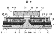
次に、本発明の第四の実施の形態について、図6を用いて説明する。実施例1〜3においては、LSI4が配線層3上にのみ実装される形態となっているが、本実施例ではLSI4の機能の一部を別体にして、それを光素子2と同じ平面上に実装した構造となっている。本実施例では、別体のLSI44a、44bは、それぞれ発光素子2aを駆動するドライバ回路、受光素子2bのフォトカレントを電圧に変換して増幅するトランスインピーダンスアンプ回路とした。LSI43は、実施例1〜3に示すLSI4から、これら回路の機能を除いたものとした。LSI44a、44b上には、光素子2a、2bと同様に絶縁層31、34が設けられている。また、LSI44a、44bは、光素子2a、2bと、表層電極パッド36とに接続されている。
Next, a fourth embodiment of the present invention will be described with reference to FIG. In the first to third embodiments, the
本実施例の製造方法は、実施例3の図5に示される方式に準ずる。LSI44a、44bともに、光素子2a、2bと同様、素子の電極パッドにAuのスタッドバンプを事前に形成し、これと基板側の電極16表面のAuとを超音波を印加されることで接合した。
The manufacturing method of the present embodiment conforms to the method shown in FIG. In both
LSI44a、44bの実装方式は、実施例1の光素子のように、回路面を上にして基板に接着し上面から電気的に接続する方法としても構わない。但し、これらLSIを固定する接着剤は、光信号が伝搬するところではないため透明である必要はない。光素子とLSIの電気的接続は同じ方式の方が、プロセスがより簡略になり望ましいが、LSIおよび光素子の電極位置によっては実施例1の構造との複合でも構わない。
The mounting method of the
なお、本実施例ではLSI44a、44bは光素子と同一平面上に搭載したが、薄膜配線層3の中の、別の平面上に設置してもよい。
In this embodiment, the
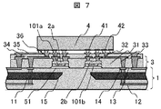
次に、本発明による第五の実施の形態を、図7および図8を用いて説明する。図7は光電気複合配線モジュールの断面図、図8はその製造方法を表す模式図である。本実施例は、光素子2と光導波路11の端部15を結ぶ光軸間に、レンズ101を備えた構造となっているのが特徴で、これにより光結合効率がさらに向上させることができる。
Next, a fifth embodiment according to the present invention will be described with reference to FIGS. FIG. 7 is a cross-sectional view of the photoelectric composite wiring module, and FIG. 8 is a schematic view showing the manufacturing method. This embodiment is characterized in that a lens 101 is provided between the optical axes connecting the
光素子2a、2bは、それぞれレンズ101a、101bの上部に実装されている。発光素子2aからの出射光は、ある広がり角をもって放出されるが、光軸上にレンズを設置することにより光は集光され、効率よく光導波路11に結合する。レンズの焦点距離としは、光素子のビーム広がり角、光導波路のコア寸法、それぞれの部材の位置関係などから、結合効率や位置ずれトレランスが良好になる値を、既存の光結合計算で決めればよい。受信側においては、光導波路11から伝送された光は同じくある広がり角を持って放出されるが、こちらもレンズ101bによって集光され、受光素子2bの開口に効率よく受光する。レンズの焦点距離の設定に関しては発光側と同様である。上記以外の構造に関しては、実施例1に示した図1と同様である。
The
次に、図8に従って、図7の製造方法の一例を説明する。まず、図2(a)は、光素子2a、2bとレンズ101a、101bを固定する工程を表している。光素子の発光/受光点とレンズの光軸中心とを位置合わせした後、これらをレンズ上に設けられた接合材53を用いて固定する。本実施例では接合材53に接着剤を用いたが、接合材は、それ以外の例えばはんだであっても構わない。レンズと光素子がぶつかることの無いように、レンズの曲面は、図のように接合面に対して凹んだ部分に凸状に形成されることが望ましい。また、図示していないが、レンズ101a、101bとは別に光素子のレンズと接合する側の面にレンズ曲面を形成しても構わない。もちろん、図に示されるレンズ101a、101bと光素子に形成したレンズをともに採用した、2枚レンズ系としても構わない。光素子とレンズを固定する際は、光導波路11と光素子2が効率よく光結合するために、光導波路11の端部15と位置合わせする必要がある。従って、光素子の搭載装置(マウンタまたはボンダ)は、必要な搭載精度を確保できる装置を使用した。
Next, an example of the manufacturing method of FIG. 7 will be described according to FIG. First, FIG. 2A shows a process of fixing the
このようにして作製した光素子2とレンズ101の一体部品を、回路基板の表層13に光導波路の端部15と光結合するような位置に搭載する(図2(b))。回路基板1とレンズ101とを固着する手段として、使用する光の波長に対して透明な接着剤51を用いた。接着剤51の塗布方法は、実施例1における光素子への接着剤塗布方法と同様である。搭載装置は、光素子とレンズとの固定と同様、必要な搭載精度を確保できるものを使用した。なお、搭載の手順としては、まず回路基板にレンズ101を搭載し、その後レンズ101上に光素子2を搭載するという方式を用いてもよい。また、レンズの回路基板への接合材に関しては、光路を妨げないのであれば透明でない接着剤を用いても構わない。また、光素子の回路基板側にメタライズを形成できれば、はんだ接合を用いてもよい。また、レンズ101と光素子2の側面がほぼ一致するようにすれば、絶縁層31を形成時に都合がよい。
The integrated component of the
本構造においても、図1の実施例と同じように従来技術に比べ組立容易性は向上する。またに、レンズを用いていることにより光の集光効果が得られ、光結合効率はさらに向上する。光素子とレンズの間には空気層が存在する構造であるが、接合材で光軸部分を囲む構造にすればゴミ等が付着する可能性はなく、従って光出力の低下を招くポテンシャルはない。 Also in this structure, as in the embodiment of FIG. 1, the ease of assembly is improved as compared with the prior art. In addition, by using the lens, a light condensing effect is obtained, and the optical coupling efficiency is further improved. Although there is an air layer between the optical element and the lens, there is no possibility that dust or the like will adhere if the structure surrounding the optical axis portion is made of a bonding material, and therefore there is no potential to reduce the light output. .
以降、光素子の上層に薄膜配線層3を形成するが(図(c)〜(d))、この手順に関しては、図2に示す第一の実施例と同様である。最後に第一の実施例と同様、薄膜配線層3の上にLSI4を実装して完成する(図2(f))。冗長性付与に関しても、第一の実施例と同様である。
Thereafter, the thin
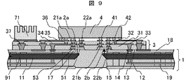
次に、本発明の第六の実施の形態について、図9を用いて説明する。実施例1〜3において、光素子の放熱は、主に光素子の電極に接続した薄膜配線層の電気配線によって行われるが、本実施例では、光素子からの発熱をより効率よく放熱するための構造が付与されている。 Next, a sixth embodiment of the present invention will be described with reference to FIG. In Examples 1 to 3, heat dissipation of the optical element is mainly performed by electrical wiring of a thin film wiring layer connected to the electrode of the optical element. In this example, heat from the optical element is more efficiently dissipated. The structure is given.
まず、第一の回路基板1の光素子2が搭載される近傍には、導体パッド17が形成されている。光素子2a、2bは、この導体パッド17上に搭載される。光素子2と導体パッド17との接合方法は、放熱性を良くするために、熱伝導率の高い接合材53を用いる。本実施例では、はんだを使用した。光素子の第一の回路基板側には、はんだを接続するための表面がAuからなるメタルパッド27を具備させた。導体パッド17は、第一の電子回路基板1の表層に広く形成された導体層18に繋がっており、この導体層18は、LSI4を基板に投影した投影面の外まで延在して基板の周辺もしくは端部まで延び、ヒートスプレッダの役割を果たす。また、導体層18は、第一の回路基板1に形成された放熱ビア19に接続しており、回路基板の下側に形成された導体層18にも放熱できる構造になっている。さらに、導体層18は、薄膜配線層3に形成された放熱用のビア37にも接続されており、これにも熱が伝わる構造となっている。放熱用ビア37は、薄膜配線層表層にて放熱部材である放熱フィン71にはんだ熱伝導のよい接合材で接続され、放熱フィン71からも放熱される。これにより、光素子からの発熱が効率よく放熱され、光電気融合配線モジュールの動作特性が安定する。
First, a
本実施例では、導体パッド17や導体層18は、放熱用の導体としてのみ用いており、図では明示されていないが、第一の回路基板1や薄膜配線層3の電気配線とは基本的には電気的に絶縁されている。しかし、これら導体パッド17や導体層18は、光素子の電極を兼ねる構造としてもよく、また、グランド配線として機能させてもよく、その場合は必要に応じ第一の回路基板の電気配線等と電気的に接続されていても構わない。また、本実施例では、放熱経路を導体層(基板の端部)、第一の回路基板の放熱ビア19、薄膜配線層の放熱ビア37と3つの経路をとっているが、モジュール全体構造や、光素子の発熱量などに応じてこれらの中の1つまたは2つのみを形成する構造としても構わない。さらに、放熱フィン71は、なくてもよいし、フィンのない導体ブロックや水冷ジャケットなど別の形態でもよいし、あるいはLSI4の冷却構造と一体形成してもよい。また、図2に示す、光素子が第二の回路基板に搭載された構造に関しても適用可能である。
In this embodiment, the
最後に、本発明による光電気融合配線モジュールが伝送装置に適用される形態を、図10を用いて説明する。なお、第一の回路基板1および親回路基板82は、簡略のため電気配線を図示していない。
Finally, an embodiment in which the optoelectric interconnection module according to the present invention is applied to a transmission apparatus will be described with reference to FIG. The
図10において、電源回路等の電気の入力は、第一の回路基板1の裏面側から供給される。本実施例では、はんだバンプ81によって親回路基板82とバンプで接合する構造となっているが、これはピンを挿入する形態のもの、あるいは電気コネクタでも構わない。一方、高速光信号は光コネクタ83により結合されている。外部からの光信号は、ここでは光ファイバ84としているが、それ以外の、光導波路フィルムや、光伝送路が形成された回路基板などでも適用可能である。
In FIG. 10, electricity input such as a power supply circuit is supplied from the back side of the
なお、本実施例では、光電気複合配線モジュールとして、図1に示される第一の形態を適用しているが、それ以外の、第二〜第四の実施の形態についても適用可能である。 In the present embodiment, the first embodiment shown in FIG. 1 is applied as the photoelectric composite wiring module, but the present invention can also be applied to other second to fourth embodiments.
本発明の実施により、高速伝送が可能で消費電力が小さく、かつ組立が容易で製造歩留りが高く、安定して動作する光電気融合配線モジュールおよびこれを用いた伝送装置が実現可能となる。 By implementing the present invention, it is possible to realize an optoelectronic interconnection module that can perform high-speed transmission, consumes low power, is easily assembled, has a high manufacturing yield, and operates stably, and a transmission apparatus using the same.
1・・・第一の回路基板、11・・・光導波路、12・・・第一の回路基板の電気配線、13・・・第一の回路基板の表層、14・・・第一の回路基板の電極パッド、15・・・光導波路の端部(45°ミラー)、16・・・電極パッド、17・・・導体パッド、18・・・導体層、19・・・第一の回路基板の放熱ビア、2・・・光素子、2a・・・発光素子(面発光型半導体レーザ)、2b・・・受光素子(面入射型フォトダイオード)、21a、21b、22a、22b、23a、23b・・・光素子の電極、24a、24b・・・スタッドバンプ、3・・・薄膜配線層、31、34・・・薄膜配線層の薄膜絶縁層、32・・・薄膜配線層のビア、33、35・・・薄膜配線層の電気配線層、36・・・薄膜配線層の電極パッド、37・・・薄膜配線層の放熱ビア、4、43・・・LSI、41・・・LSIの電極パッド、42・・・LSI接合バンプ、44a・・・LSI(ドライバ回路)、44b・・・LSI(トランスインピーダンスアンプ回路)、51・・・接着剤、52・・・樹脂、53・・・接合材(接着剤)、6・・・第二の回路基板、61・・・第二の回路基板の絶縁基板、62、62・・・第二の回路基板の配線、64・・・第二の回路基板のスルーホール、65・・・はんだ、71・・・放熱部材(放熱フィン)、81・・・はんだバンプ、82・・・親回路基板、83・・・光コネクタ、84・・・光伝送路(光ファイバ)、91・・・光信号、101a、101b・・・レンズ。
DESCRIPTION OF
Claims (28)
前記第一の回路基板上に設けられ、前記光導波路と光結合する光素子と、
前記第一の回路基板及び前記光素子上に設けられた絶縁膜と、
前記絶縁膜上に設けられた配線パッドと、
前記光素子と前記配線パッドを電気的に接続する電気配線と、
前記配線パッド上に設けられて電気的に接続される第一の半導体素子とを備え、
前記光素子は、前記第一の回路基板の前記第一の半導体素子側の面であり、かつ前記第一の半導体素子を前記第一の回路基板に投影した投影面内に設けられていることを特徴とする光電気複合配線モジュール。 A first circuit board having an optical waveguide for propagating an optical signal;
An optical element provided on the first circuit board and optically coupled to the optical waveguide;
An insulating film provided on the first circuit board and the optical element;
A wiring pad provided on the insulating film;
Electrical wiring for electrically connecting the optical element and the wiring pad;
A first semiconductor element provided on the wiring pad and electrically connected;
The optical element is a surface of the first circuit board on the first semiconductor element side, and is provided in a projection plane obtained by projecting the first semiconductor element onto the first circuit board. An opto-electric composite wiring module.
前記光素子は、前記第一の半導体素子と前記光導波路との間に設けられていることを特徴とする光電気複合配線モジュール。 In claim 1,
The optoelectric composite wiring module, wherein the optical element is provided between the first semiconductor element and the optical waveguide.
前記光素子は、当該光素子が接続される前記配線パッドの直下にあることを特徴とする光電気複合配線モジュール。 In claim 1,
The photoelectric composite wiring module according to claim 1, wherein the optical element is directly below the wiring pad to which the optical element is connected.
前記光素子は、当該光素子が接続される前記配線パッドと、当該光素子が光結合する光導波路との間に配置されていることを特徴とする光電気複合配線モジュール。 In claim 3,
The optical composite wiring module, wherein the optical element is arranged between the wiring pad to which the optical element is connected and an optical waveguide to which the optical element is optically coupled.
前記光素子と前記配線パッドとは、前記絶縁膜内に形成されたビアにより接続されていることを特徴とする光電気複合配線モジュール。 In claim 1,
The opto-electric composite wiring module, wherein the optical element and the wiring pad are connected by a via formed in the insulating film.
前記光素子は、その前記第一の半導体素子側に、前記ビアに接続される電極を有することを特徴とする光電気複合配線モジュール。 In claim 5,
The optoelectric composite wiring module according to claim 1, wherein the optical element has an electrode connected to the via on the first semiconductor element side.
前記光素子は、その前記前記第一の回路基板側に、前記回路基板上の電極と接続された電極を有することを特徴とする光電気複合配線モジュール。 In claim 1,
The optoelectric composite wiring module according to claim 1, wherein the optical element has an electrode connected to an electrode on the circuit board on the first circuit board side.
前記光素子を搭載する第二の回路基板を有し、
当該第二の基板は、前記光素子を前記第一の回路基板に向けて搭載されていることを特徴とする光電気複合配線モジュール。 In claim 1,
A second circuit board on which the optical element is mounted;
The optoelectric composite wiring module according to claim 2, wherein the second substrate is mounted with the optical element facing the first circuit substrate.
前記第一の回路基板に上に搭載された第二の半導体素子を備え、
当該第二の半導体素子の上に前記絶縁膜が設けられており、
当該第二の半導体素子は、前記光素子と前記第一の半導体素子とに電気的に接続されていることを特徴とする光電気複合配線モジュール。 In claim 1,
A second semiconductor element mounted on the first circuit board;
The insulating film is provided on the second semiconductor element,
The photoelectric composite wiring module, wherein the second semiconductor element is electrically connected to the optical element and the first semiconductor element.
前記光素子と前記光導波路との光軸間にレンズが設けられていることを特徴とする光電気複合配線モジュール。 In claim 1,
A photoelectric composite wiring module, wherein a lens is provided between optical axes of the optical element and the optical waveguide.
前記第一の回路基板は、その表面に、前記光素子に接続された導体層を有し、
当該導体層は、前記半導体素子の投影面の外まで延在していることを特徴とする光電気複合配線モジュール。 In claim 1,
The first circuit board has a conductor layer connected to the optical element on the surface thereof,
The said electrical conductor layer is extended outside the projection surface of the said semiconductor element, The photoelectric composite wiring module characterized by the above-mentioned.
前記第一の回路基板は、前記光素子を搭載した側の表面及びその反対側の表面の両面に前記導体層を有し、
前記両面の導体層は、ビアにより互いに接続されていることを特徴とする光電気複合配線モジュール。 In claim 11,
The first circuit board has the conductor layer on both the surface on which the optical element is mounted and the opposite surface.
The photoelectric composite wiring module, wherein the conductor layers on both sides are connected to each other by vias.
前記絶縁膜上に放熱フィンを有し、
当該放熱フィンと前記導体層は接続されていることを特徴とする光電気複合配線モジュール。 In claim 11,
A heat dissipating fin on the insulating film;
The photoelectric composite wiring module, wherein the radiation fin and the conductor layer are connected.
前記光導波路は、前記光素子と光結合した側と反対の端部を、光ファイバと光結合し、
光電気複合配線モジュールの有する電気配線が、モジュール外部の電気配線と電気的に接合されていることを特徴とする伝送装置。 The photoelectric composite wiring module according to claim 1,
The optical waveguide is optically coupled with an optical fiber at an end opposite to the side optically coupled with the optical element,
A transmission device, wherein electrical wiring of the photoelectric composite wiring module is electrically joined to electrical wiring outside the module.
前記回路基板及び前記光素子上に絶縁膜を形成する工程と、
前記絶縁膜内に、前記光素子に接続される電気配線を形成する工程と、
前記絶縁膜上に、前記電気配線に接続される配線パッドを形成する工程と、
前記配線パッドに半導体素子を接続する工程とを含む光電気複合配線モジュールの製造方法。 Mounting an optical element on the first circuit board having an optical waveguide so as to be optically coupled to the optical waveguide;
Forming an insulating film on the circuit board and the optical element;
Forming an electrical wiring connected to the optical element in the insulating film;
Forming a wiring pad connected to the electrical wiring on the insulating film;
And a step of connecting a semiconductor element to the wiring pad.
前記半導体素子は、前記光素子が搭載された領域の上の領域に搭載されることを特徴とする光電気複合配線モジュールの製造方法。 In claim 15,
The method of manufacturing an opto-electric composite wiring module, wherein the semiconductor element is mounted in a region above the region where the optical element is mounted.
前記光素子は、前記半導体素子と前記光導波路との間に設けられていることを特徴とする光電気複合配線モジュールの製造方法。 In claim 16,
The method of manufacturing an optical / electrical interconnect module, wherein the optical element is provided between the semiconductor element and the optical waveguide.
前記配線パッドは、当該配線パッドが接続される前記光素子の直上にあることを特徴とする光電気複合配線モジュールの製造方法。 In claim 15,
The method of manufacturing an opto-electric composite wiring module, wherein the wiring pad is directly above the optical element to which the wiring pad is connected.
前記光素子は、当該光素子が接続される前記配線パッドと、当該光素子が光結合する光導波路との間に配置されていることを特徴とする光電気複合配線モジュールの製造方法。 In claim 18,
The method of manufacturing a photoelectric composite wiring module, wherein the optical element is disposed between the wiring pad to which the optical element is connected and an optical waveguide to which the optical element is optically coupled.
前記光素子と前記配線パッドとは、前記絶縁膜内に形成されたビアにより接続されていることを特徴とする光電気複合配線モジュールの製造方法。 In claim 15,
The method of manufacturing an optical / electrical interconnect module, wherein the optical element and the wiring pad are connected by a via formed in the insulating film.
前記光素子は、その前記半導体素子側に、前記ビアに接続される電極を有することを特徴とする光電気複合配線モジュールの製造方法。 In claim 20,
The method of manufacturing an optical / electrical interconnect module, wherein the optical element has an electrode connected to the via on the semiconductor element side.
前記光素子は、その前記前記第一の回路基板側に、前記回路基板上の電極と接続される電極を有することを特徴とする光電気複合配線モジュールの製造方法。 In claim 15,
The said optical element has an electrode connected with the electrode on the said circuit board in the said 1st circuit board side, The manufacturing method of the photoelectric composite wiring module characterized by the above-mentioned.
前記光素子は、当該光素子を搭載する第二の回路基板を有しており、
当該光素子は、前記第二の回路基板を前記第一の回路基板とは反対側に向けて搭載されることを特徴とする光電気複合配線モジュールの製造方法。 In claim 15,
The optical element has a second circuit board on which the optical element is mounted,
The optical element is mounted with the second circuit board facing the opposite side of the first circuit board.
前記第一の回路基板上に、第二の半導体素子を搭載する工程を含み、
前記絶縁膜は、前記第二の半導体素子上にも形成され、
前記電気配線は、前記第二の半導体素子にも接続されることを特徴とする光電気複合配線モジュールの製造方法。 In claim 15,
Mounting a second semiconductor element on the first circuit board;
The insulating film is also formed on the second semiconductor element,
The method of manufacturing an optical / electrical interconnect module, wherein the electrical wiring is also connected to the second semiconductor element.
前記光素子と前記光導波路との光軸間にレンズ設置する工程を含むことを特徴とする光電気複合配線モジュールの製造方法。 In claim 15,
A method of manufacturing a photoelectric composite wiring module comprising a step of installing a lens between optical axes of the optical element and the optical waveguide.
前記第一の回路基板は、その表面に導体層を有し、
前記導体層は、前記光素子に接続され、
前記導体層は、前記半導体素子の投影面の外まで延在していることを特徴とする光電気複合配線モジュールの製造方法。 In claim 15,
The first circuit board has a conductor layer on its surface;
The conductor layer is connected to the optical element;
The method for manufacturing an opto-electric composite wiring module, wherein the conductor layer extends to the outside of a projection surface of the semiconductor element.
前記第一の回路基板は、前記光素子を搭載する側の表面及びその反対側の表面の両面に前記導体層を有し、
前記両面の導体層は、ビアにより互いに接続されていることを特徴とする光電気複合配線モジュールの製造方法。 In claim 26,
The first circuit board has the conductor layer on both the surface on the side on which the optical element is mounted and the opposite surface.
The method for manufacturing an opto-electric composite wiring module, wherein the conductor layers on both sides are connected to each other by vias.
前記絶縁膜上の前記導体層に接続されるビアの上に放熱フィンを搭載する工程を有することを特徴とする光電気複合配線モジュールの製造方法。 In claim 26,
A method for manufacturing an optoelectronic composite wiring module, comprising a step of mounting a radiation fin on a via connected to the conductor layer on the insulating film.
Priority Applications (5)
| Application Number | Priority Date | Filing Date | Title |
|---|---|---|---|
| JP2009233978A JP2010211179A (en) | 2009-02-13 | 2009-10-08 | Photoelectric composite wiring module and method for manufacturing the same |
| US12/623,686 US8401347B2 (en) | 2009-02-13 | 2009-11-23 | Photoelectric composite wiring module and method for manufacturing the same |
| CN200910251208.XA CN101900859B (en) | 2009-02-13 | 2009-12-02 | Photoelectric composite wiring module and method for manufacturing the same |
| KR1020090118963A KR20100092861A (en) | 2009-02-13 | 2009-12-03 | Optoelectric complex wring module and manufacturing method thereof |
| KR1020120053251A KR101238977B1 (en) | 2009-02-13 | 2012-05-18 | Optoelectric complex wiring module and manufacturing method thereof |
Applications Claiming Priority (2)
| Application Number | Priority Date | Filing Date | Title |
|---|---|---|---|
| JP2009030637 | 2009-02-13 | ||
| JP2009233978A JP2010211179A (en) | 2009-02-13 | 2009-10-08 | Photoelectric composite wiring module and method for manufacturing the same |
Publications (2)
| Publication Number | Publication Date |
|---|---|
| JP2010211179A true JP2010211179A (en) | 2010-09-24 |
| JP2010211179A5 JP2010211179A5 (en) | 2012-02-09 |
Family
ID=42559962
Family Applications (1)
| Application Number | Title | Priority Date | Filing Date |
|---|---|---|---|
| JP2009233978A Pending JP2010211179A (en) | 2009-02-13 | 2009-10-08 | Photoelectric composite wiring module and method for manufacturing the same |
Country Status (4)
| Country | Link |
|---|---|
| US (1) | US8401347B2 (en) |
| JP (1) | JP2010211179A (en) |
| KR (2) | KR20100092861A (en) |
| CN (1) | CN101900859B (en) |
Cited By (5)
| Publication number | Priority date | Publication date | Assignee | Title |
|---|---|---|---|---|
| JP2014089262A (en) * | 2012-10-29 | 2014-05-15 | Shinko Electric Ind Co Ltd | Optical waveguide, optical module and method of manufacturing optical waveguide |
| KR101856230B1 (en) * | 2011-12-09 | 2018-05-09 | 엘지이노텍 주식회사 | Optical Printed Circuit Board and Fabricating method of the same |
| KR101856229B1 (en) * | 2011-12-09 | 2018-05-09 | 엘지이노텍 주식회사 | Optical Printed Circuit Board and Fabricating method of the same |
| WO2018180785A1 (en) * | 2017-03-30 | 2018-10-04 | 京セラ株式会社 | Photoelectric wiring substrate |
| WO2019117035A1 (en) * | 2017-12-12 | 2019-06-20 | 日東電工株式会社 | Photoelectric mixed substrate |
Families Citing this family (15)
| Publication number | Priority date | Publication date | Assignee | Title |
|---|---|---|---|---|
| DE102009001930B4 (en) * | 2009-03-27 | 2018-01-04 | Robert Bosch Gmbh | sensor module |
| EP2428828B1 (en) * | 2010-09-13 | 2016-06-29 | Tyco Electronics Svenska Holdings AB | Miniaturized high speed optical module |
| EP2643725A1 (en) * | 2010-11-25 | 2013-10-02 | Fci | Optical circuit board |
| KR101256000B1 (en) * | 2011-04-13 | 2013-04-18 | 엘지이노텍 주식회사 | Interposer for optical module and Fabricating method of the same, Optical module using the same |
| CN104115043B (en) * | 2011-12-08 | 2019-09-17 | Lg伊诺特有限公司 | Optical printed circuit board and its manufacturing method |
| WO2013095426A1 (en) * | 2011-12-21 | 2013-06-27 | Intel Corporation | Fabrication of planar light-wave circuits (plcs) for optical i/o |
| JP6136545B2 (en) * | 2013-05-07 | 2017-05-31 | 日立金属株式会社 | OPTICAL WIRING BOARD, OPTICAL WIRING BOARD MANUFACTURING METHOD, AND OPTICAL MODULE |
| WO2015029680A1 (en) * | 2013-09-02 | 2015-03-05 | 株式会社村田製作所 | Isolator |
| JP6287105B2 (en) * | 2013-11-22 | 2018-03-07 | ソニー株式会社 | Optical communication device, receiving apparatus, transmitting apparatus, and transmitting / receiving system |
| AT14563U1 (en) * | 2014-03-31 | 2016-01-15 | At&S Austria Technologie & Systemtechnik Ag | Method for producing a printed circuit board with at least one optoelectronic component |
| WO2015174239A1 (en) * | 2014-05-13 | 2015-11-19 | ソニー株式会社 | Photoelectric module and optical element |
| CN108627845B (en) * | 2017-03-15 | 2021-05-28 | 信泰光学(深圳)有限公司 | Circuit layout structure of laser driving circuit |
| CN109752804B (en) * | 2017-11-06 | 2020-11-10 | 松下知识产权经营株式会社 | Optical module structure |
| US20230341642A1 (en) * | 2019-12-27 | 2023-10-26 | Nitto Denko Corporation | Opto-electric hybrid board |
| KR20230082333A (en) * | 2021-12-01 | 2023-06-08 | 삼성전기주식회사 | Printed circuit board and printed circuit board package |
Citations (5)
| Publication number | Priority date | Publication date | Assignee | Title |
|---|---|---|---|---|
| WO1999017142A1 (en) * | 1997-10-01 | 1999-04-08 | Hitachi Chemical Company, Ltd. | Optical information processor |
| JP2004163722A (en) * | 2002-11-14 | 2004-06-10 | Fujitsu Ltd | Component-incorporated substrate |
| JP2004274155A (en) * | 2003-03-05 | 2004-09-30 | Canon Inc | Optical connector and optical and electrical hybrid device |
| JP2006270037A (en) * | 2005-02-28 | 2006-10-05 | Sony Corp | Hybrid module, its manufacturing process and hybrid circuit device |
| JP2007183522A (en) * | 2005-01-19 | 2007-07-19 | Bridgestone Corp | Optical device and method for producing the same |
Family Cites Families (19)
| Publication number | Priority date | Publication date | Assignee | Title |
|---|---|---|---|---|
| US6693736B1 (en) * | 1992-09-10 | 2004-02-17 | Fujitsu Limited | Optical circuit system and components of same |
| JP2004233991A (en) | 1997-10-01 | 2004-08-19 | Hitachi Chem Co Ltd | Optical information processor |
| JP2001183556A (en) | 1999-12-27 | 2001-07-06 | Toppan Printing Co Ltd | Multi-chip module board and multi-chip module |
| JP3750649B2 (en) * | 2001-12-25 | 2006-03-01 | 住友電気工業株式会社 | Optical communication device |
| JP3882738B2 (en) * | 2002-10-24 | 2007-02-21 | ソニー株式会社 | Composite chip module and manufacturing method thereof, and composite chip unit and manufacturing method thereof |
| JP2004177521A (en) | 2002-11-25 | 2004-06-24 | Fujitsu Ltd | Optical and electrical combined circuit board |
| JP3897688B2 (en) * | 2002-12-11 | 2007-03-28 | キヤノン株式会社 | Optoelectronic wiring board |
| JP3913175B2 (en) * | 2003-01-06 | 2007-05-09 | キヤノン株式会社 | Information transmission method in optical circuit device |
| JP4845333B2 (en) | 2003-04-11 | 2011-12-28 | 株式会社リコー | Photoelectric conversion element package, manufacturing method thereof, and optical connector |
| US6985645B2 (en) * | 2003-09-24 | 2006-01-10 | International Business Machines Corporation | Apparatus and methods for integrally packaging optoelectronic devices, IC chips and optical transmission lines |
| EP1688770B1 (en) * | 2003-11-27 | 2012-11-14 | Ibiden Co., Ltd. | Ic chip mounting board, substrate for mother board, device for optical communication, method for manufacturing substrate for mounting ic chip thereon, and method for manufacturing substrate for mother board |
| US7271461B2 (en) * | 2004-02-27 | 2007-09-18 | Banpil Photonics | Stackable optoelectronics chip-to-chip interconnects and method of manufacturing |
| US7092603B2 (en) * | 2004-03-03 | 2006-08-15 | Fujitsu Limited | Optical bridge for chip-to-board interconnection and methods of fabrication |
| US7373034B2 (en) * | 2004-09-02 | 2008-05-13 | Nec Corporation | Optoelectronic hybrid integrated module |
| JP2006133763A (en) | 2004-10-07 | 2006-05-25 | Nec Corp | Structure and method of mounting lsi package to photoelectric wiring board, information processing apparatus, optical interface and photoelectric wiring board |
| WO2006095676A1 (en) * | 2005-03-07 | 2006-09-14 | Rohm Co., Ltd. | Optical communication module and manufacturing method thereof |
| TWI309549B (en) * | 2005-08-29 | 2009-05-01 | Via Tech Inc | Printed circuit board with improved thermal dissipating structure and electronic device with the same |
| JP4533283B2 (en) * | 2005-08-29 | 2010-09-01 | 新光電気工業株式会社 | Manufacturing method of semiconductor device |
| US7778501B2 (en) * | 2007-04-03 | 2010-08-17 | Hewlett-Packard Development Company, L.P. | Integrated circuits having photonic interconnect layers and methods for fabricating same |
-
2009
- 2009-10-08 JP JP2009233978A patent/JP2010211179A/en active Pending
- 2009-11-23 US US12/623,686 patent/US8401347B2/en not_active Expired - Fee Related
- 2009-12-02 CN CN200910251208.XA patent/CN101900859B/en not_active Expired - Fee Related
- 2009-12-03 KR KR1020090118963A patent/KR20100092861A/en active Search and Examination
-
2012
- 2012-05-18 KR KR1020120053251A patent/KR101238977B1/en not_active IP Right Cessation
Patent Citations (5)
| Publication number | Priority date | Publication date | Assignee | Title |
|---|---|---|---|---|
| WO1999017142A1 (en) * | 1997-10-01 | 1999-04-08 | Hitachi Chemical Company, Ltd. | Optical information processor |
| JP2004163722A (en) * | 2002-11-14 | 2004-06-10 | Fujitsu Ltd | Component-incorporated substrate |
| JP2004274155A (en) * | 2003-03-05 | 2004-09-30 | Canon Inc | Optical connector and optical and electrical hybrid device |
| JP2007183522A (en) * | 2005-01-19 | 2007-07-19 | Bridgestone Corp | Optical device and method for producing the same |
| JP2006270037A (en) * | 2005-02-28 | 2006-10-05 | Sony Corp | Hybrid module, its manufacturing process and hybrid circuit device |
Cited By (7)
| Publication number | Priority date | Publication date | Assignee | Title |
|---|---|---|---|---|
| KR101856230B1 (en) * | 2011-12-09 | 2018-05-09 | 엘지이노텍 주식회사 | Optical Printed Circuit Board and Fabricating method of the same |
| KR101856229B1 (en) * | 2011-12-09 | 2018-05-09 | 엘지이노텍 주식회사 | Optical Printed Circuit Board and Fabricating method of the same |
| JP2014089262A (en) * | 2012-10-29 | 2014-05-15 | Shinko Electric Ind Co Ltd | Optical waveguide, optical module and method of manufacturing optical waveguide |
| WO2018180785A1 (en) * | 2017-03-30 | 2018-10-04 | 京セラ株式会社 | Photoelectric wiring substrate |
| WO2019117035A1 (en) * | 2017-12-12 | 2019-06-20 | 日東電工株式会社 | Photoelectric mixed substrate |
| JP2019105718A (en) * | 2017-12-12 | 2019-06-27 | 日東電工株式会社 | Photoelectric mixed substrate |
| JP7176842B2 (en) | 2017-12-12 | 2022-11-22 | 日東電工株式会社 | opto-electric hybrid board |
Also Published As
| Publication number | Publication date |
|---|---|
| US20100209041A1 (en) | 2010-08-19 |
| US8401347B2 (en) | 2013-03-19 |
| KR20100092861A (en) | 2010-08-23 |
| CN101900859B (en) | 2014-11-05 |
| KR101238977B1 (en) | 2013-03-04 |
| KR20120061788A (en) | 2012-06-13 |
| CN101900859A (en) | 2010-12-01 |
Similar Documents
| Publication | Publication Date | Title |
|---|---|---|
| KR101238977B1 (en) | Optoelectric complex wiring module and manufacturing method thereof | |
| JP5178650B2 (en) | Photoelectric composite wiring module and manufacturing method thereof | |
| JP5439080B2 (en) | Optical I / O array module | |
| JP4425936B2 (en) | Optical module | |
| KR100460703B1 (en) | Electro-optical circuit board having unified optical transmission/receiving module and optical waveguide | |
| JP4859677B2 (en) | Photovoltaic module fabrication system and method | |
| US9647762B2 (en) | Integrated parallel optical transceiver | |
| TW200536134A (en) | Lsi package provided with interface module, and transmission line header employed in the package | |
| Doany et al. | Terabit/sec-class board-level optical interconnects through polymer waveguides using 24-channel bidirectional transceiver modules | |
| JP2009003253A (en) | Structure of photo-electric hybrid substrate and photo-electric package | |
| JP2011081071A (en) | Optical module | |
| JP2012226342A (en) | Optical module, method of manufacturing optical module, and optical communication device | |
| CN103579376A (en) | Opto-electronic system having flip-chip substrate mounting | |
| JP4246563B2 (en) | Optical component support substrate and manufacturing method thereof, optical component support substrate with optical component and manufacturing method thereof | |
| JP2008041772A (en) | Optical module | |
| WO2012020532A1 (en) | Photoelectric composite wiring module and method for manufacturing same | |
| JP2012013726A (en) | Optical interconnection module, and optical and electrical circuit board using the same | |
| JPWO2009001822A1 (en) | Optical module | |
| WO2014141458A1 (en) | Optical module and transmitting device | |
| JP2012088634A (en) | Optical waveguide device and method for manufacturing the same | |
| JP5981145B2 (en) | Circuit board and communication system | |
| KR101071550B1 (en) | A photoelectric conversion module | |
| WO2014069290A1 (en) | Connection structure between lenses, optical equipment, photoelectric composite wiring module, and transmission device | |
| TW201409103A (en) | Photoelectric PCB for accurately aligning the light source |
Legal Events
| Date | Code | Title | Description |
|---|---|---|---|
| A521 | Request for written amendment filed |
Free format text: JAPANESE INTERMEDIATE CODE: A523 Effective date: 20111215 |
|
| A621 | Written request for application examination |
Free format text: JAPANESE INTERMEDIATE CODE: A621 Effective date: 20111215 |
|
| A977 | Report on retrieval |
Free format text: JAPANESE INTERMEDIATE CODE: A971007 Effective date: 20121120 |
|
| A131 | Notification of reasons for refusal |
Free format text: JAPANESE INTERMEDIATE CODE: A131 Effective date: 20130717 |
|
| A521 | Request for written amendment filed |
Free format text: JAPANESE INTERMEDIATE CODE: A523 Effective date: 20130826 |
|
| A131 | Notification of reasons for refusal |
Free format text: JAPANESE INTERMEDIATE CODE: A131 Effective date: 20130910 |
|
| A02 | Decision of refusal |
Free format text: JAPANESE INTERMEDIATE CODE: A02 Effective date: 20140128 |