JP3913175B2 - Information transmission method in optical circuit device - Google Patents
Information transmission method in optical circuit device Download PDFInfo
- Publication number
- JP3913175B2 JP3913175B2 JP2003000017A JP2003000017A JP3913175B2 JP 3913175 B2 JP3913175 B2 JP 3913175B2 JP 2003000017 A JP2003000017 A JP 2003000017A JP 2003000017 A JP2003000017 A JP 2003000017A JP 3913175 B2 JP3913175 B2 JP 3913175B2
- Authority
- JP
- Japan
- Prior art keywords
- port
- transmission
- light
- optical
- radiation angle
- Prior art date
- Legal status (The legal status is an assumption and is not a legal conclusion. Google has not performed a legal analysis and makes no representation as to the accuracy of the status listed.)
- Expired - Fee Related
Links
Images


Classifications
-
- G—PHYSICS
- G02—OPTICS
- G02B—OPTICAL ELEMENTS, SYSTEMS OR APPARATUS
- G02B6/00—Light guides; Structural details of arrangements comprising light guides and other optical elements, e.g. couplings
- G02B6/24—Coupling light guides
- G02B6/42—Coupling light guides with opto-electronic elements
- G02B6/43—Arrangements comprising a plurality of opto-electronic elements and associated optical interconnections
-
- H—ELECTRICITY
- H04—ELECTRIC COMMUNICATION TECHNIQUE
- H04B—TRANSMISSION
- H04B10/00—Transmission systems employing electromagnetic waves other than radio-waves, e.g. infrared, visible or ultraviolet light, or employing corpuscular radiation, e.g. quantum communication
- H04B10/80—Optical aspects relating to the use of optical transmission for specific applications, not provided for in groups H04B10/03 - H04B10/70, e.g. optical power feeding or optical transmission through water
- H04B10/801—Optical aspects relating to the use of optical transmission for specific applications, not provided for in groups H04B10/03 - H04B10/70, e.g. optical power feeding or optical transmission through water using optical interconnects, e.g. light coupled isolators, circuit board interconnections
Description
【0001】
【発明の属する技術分野】
本発明は、光信号を発信する機能を有した発信ポートと光信号を受信する機能を有した受信ポートの間で光伝送媒体を介して光による情報伝達を行なう情報伝達方法に関し、特には、発信ポートと受信ポートの間で柔軟に光回路を形成して情報を伝達する情報伝達方法に関する。
【0002】
【従来の技術】
最近、パーソナルコンピューター、更には携帯電話や個人情報端末(PDA)などの情報処理機器は、処理速度の速いことと小型・軽量であることに加えて、複数のアプリケーションを切り替えて用いることが望まれている。他方で、ロボットなどの制御機器においては、複数の制御アルゴリズムをリアルタイムで切り替えて制御することが望まれる。この様な視点から、回路の再構成が可能な回路基板、特に高速でリアルタイムに回路の再構成を可能とする回路基板が望まれている。
【0003】
従来は、電子回路、スイッチ、メモリなどでこの様な回路を実現しようとすることが一般的であったが、処理速度が上がるにつれて、配線遅延、EMI(電磁放射干渉ノイズ)などの問題が生じる。こうした配線遅延やEMIを回避する手法としては、高速伝送が可能で本質的に電磁無誘導の利点を有する光配線を用いることが挙げられる(例えば、特許文献1参照)。
【0004】
【特許文献1】
特開平5-67770号公報
【0005】
【発明が解決しようとする課題】
しかし、上述の特許文献1等の光配線方法は、光配線形成の柔軟性が足りなかった。
【0006】
本発明の目的は、上記の課題に鑑み、発信ポートと受信ポートを備えた光回路装置において発信ポートと受信ポートの間で柔軟に光回路を形成して情報伝達を行なえる情報伝達方法を提供することにある。
【0007】
【課題を解決するための手段】
上記目的を達成する本発明の第1の情報伝達方法は、光信号を発信する機能を有した発信ポートと光信号を受信する機能を有した複数の受信ポートと光信号を伝播する光伝送シートを備えた光回路装置において発信ポートと受信ポートの間で光伝送シートを介して情報を伝達する情報伝達方法であって、発信ポートから光伝送シート内に第1の放射角領域で光を放出して少なくとも2つの受信ポートに対して第1の情報伝達を行なう第1のステップと、該第1のステップの後で、該発信ポートから該第1の放射角領域より狭い第2の放射角領域で光を放出して少なくとも1つの受信ポートに対して第2の情報伝達を行なう第2のステップを含む伝送により、第 1 のステップと第2のステップは共同して所期の情報伝達を行なうことを特徴とする。また、上記目的を達成する本発明の第2の情報伝達方法は、光信号を発信する機能を有した発信ポートと光信号を受信する機能を有した複数の受信ポートと光信号を伝播する光伝送シートを備えた光回路装置において発信ポートと受信ポートの間で光伝送シートを介して情報を伝達する情報伝達方法であって、発信ポートから光伝送シート内に第1の放射角領域で光を放出して1つの受信ポートに対して第1の情報伝達を行なう第1のステップと、該第1のステップの後で、該発信ポートから該第1の放射角領域より大きい第2の放射角領域で光を放出して複数の受信ポートに対して第2の情報伝達を行なう第2のステップを含む伝送により、第 1 のステップと第2のステップは共同して所期の情報伝達を行なうことを特徴とする。この情報伝達方法では、発信ポートから異なる放射角領域で光を放出する複数のステップを用いるので、この発信ポートと受信ポートの間で柔軟に光回路を形成して光信号を伝送して所期の情報伝達を行なえる。各ステップでどの様な情報内容の光伝送を行なうかは、利用する通信プロトコル、伝送目的などに応じて種々に決められる。また、各ステップにおいて、発信ポートからの光の放射角領域により受信可能な受信ポートは決まるが、受信可能な受信ポートが全て受信を行なう必要はなく、受信するか否かは受信ポート側で決めてもよい。
【0008】
上記基本の情報伝達方法において、前記第1のステップで、前記発信ポートと少なくとも1つの受信ポート間で通信経路の確立を行い、引き続き、前記第2のステップで、該通信経路を用いてデータ伝送を行い、第1のステップにおいて発信ポートから放出される光の放射角領域が、第2のステップにおいて発信ポ一トから放出される放射角領域よりも大きい様にできる。また、前記第1のステップにおけるデータ転送速度を第2のステップにおけるデータ転送速度よりも遅くして確実且つ効率良く情報伝達を行なうこともできる。
【0009】
また、少なくとも以下の手続きを経て、確実に光による情報伝達を行なう様にもできる、
1)ポートAから通信要求信号を第1の放射角領域で複数のポートへ発信、
2)通信要求信号を受信した複数のポートのうち、ポートBが受信可能信号をポートAに返信、
3)ポートAからポートBに向けて第1の放射角領域より小さい第2の放射角領域でデータを送信。
【0010】
さらに、前記受信可能信号は、電気配線を用いて伝達がなされる様にしたり、第1のステップで情報を受信するポートの数が、第2のステップにおいて情報を受信するポートの数より多い様にすることもできる。
【0013】
【発明の実施の形態】
以下に具体的な実施例をあげて、本発明の実施の形態を説明する。ただし、本発明は、以下に示す実施例に限られるものではなく、上述の基本構成概念に含まれるものであれば、その具体的構成などは問わない。
【0014】
(実施例1)
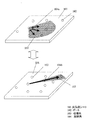
本発明の実施例1における回路基板は、光回路と電子回路が混在した回路基板であって、光信号を発信もしくは受信する機能を有した光ポートの間で光による情報伝達が可能なように構成されている。情報発信を行なう発信ポートの光出力部は、2種類以上の放射角領域の中から所望の放射角領域に切り替えて2次元(2D)光導波路(光伝送シート)内に光を伝播させる手段を有しており、この切り替え手段により、ポート間の光による情報伝達が実現される。図1は、本実施例において或るポート102から2D光導波路101に光103を伝播させる場合の異なる放射角領域104a、104bの例を示す。ここで、放射角領域とは、図1に示すよう、光伝送媒体が2D光導波路101である場合にはx−y平面における放射角φaである。この平面に垂直なz方向においては、伝播可能な全ての角度(全ての導波モード)を伝播させたり、選ばれた角度(単一の伝播モード)を伝播させたりできるが、特にこだわらない。本明細書において、2D光導波路の場合の「放射角領域」は特に言及しない限りx−y平面における放射角を意味するものとする。また、光伝送媒体が3次元の光導波路や自由空間などである場合は、「放射角領域」は発信ポートから放射される光の立体角を意味するものとする。
【0015】
図2は実施例1における回路基板を説明する模式断面図である。図2の回路基板の構造例において、100は全体の基板、101は2D光導波路である光伝送シート、102は光伝送シート101と電気配線層105の界面付近に設けられた光入力(受信)或いは出力(発信)ポート、103は光伝送シート(光配線層)101内の伝播光、105は光伝送シート101を挟んで設けられた電気配線層、106は電気配線層105内の電気配線、107は電気配線層105上に設けられたLSIなどの電子デバイスである。
【0016】
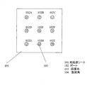
図2の構成例の場合、光配線層101を一対の電気配線層105が挟む構成になっており、電気配線層105aと光配線層101の界面付近に光ポート102を設置してある。この様にポート102は光伝送シート101に接して上部に配置しているが、これに限らず、光伝送シート101の中に埋め込むように配置し、直接、導波路に光を結合してもよいし、光伝送シート101の端面に配置してもよい。また、図2では、3つのポート102を有した回路とされ、発信を担うポート1つ(102a)と、受信を行なうポート1つ(102c)が設けられているが、これも例示である。光伝送シート(光配線層)101の上から見た配置において、図1に示す様にポート102を配することもできるし、図3の様に碁盤目状に配することもできる。要するに、面内に任意の数のポートを任意の位置に配置可能である。光伝送シート101のサイズは、2Dの任意位置間で情報伝達を行なうことから、情報伝達速度にもよるが、例えば100ミクロン程度から数10cmである。本実施例では、基板のサイズは3cm角である。
【0017】
図2に示す様に、本実施例における回路基板は、電子デバイス107とそれらを接続する電気配線106を有した電子回路と、光伝送シート101を伝送媒体として用いた光回路が共存している。こうした構成において、電子デバイス107からの信号は、ポート102aにおいて光信号に変換され、光信号は光伝送シート101を伝播後、別のポート102cにおいて電気信号に変換される。
【0018】
以下に、各要素について更に詳細に説明する。
本実施例では、光伝送シート101としては、厚さ100μmのポリカーボネート(屈折率1.59)にクラッドとしてフッ素化ポリイミド(屈折率1.52程度)をコートしたものを用いた。光伝送シート101は、電子デバイス107が実装されたプリント基板を積層、接着することで、図2に示す様に積層された高密度実装された回路基板とできる。光伝送シート101は、或る程度に2次元状に広がった光導波路である2次元導波路を適用した光伝送媒体であり、任意の位置に光デバイスを配置でき、任意の点に配したポート102から任意のポート102に2次元的に光データを送信できる。勿論、光伝送シート101は、上記の例に限らず、伝播光に対して十分な透過率を有するものであれば、ガラス、半導体、有機材料などの任意の材料を使用できる。例えば、市販のガラス基板、ニオブ酸リチウムなどの単結晶基板、Si,GaAsなどの半導体基板、ポリカーボネート、アクリル、ポリイミド、ポリエチレンテレフタラートなどからなる有機シートなどを、そのまま用いられる。また、真空蒸着、ディッピング、塗布などの任意の手法で製膜することや、射出成型、押し出し成型などで成型して作製する方法などを用いて形成される。光伝送シート101の厚さは、1ミクロン程度から数cmの範囲で可能であるが、光軸合わせの容易性の観点から50ミクロンから数ミリ程度の厚さが好ましい(上記例では、100ミクロン程度である)。
【0019】
光伝送シート101は任意の基板100上に配し得る。基板100としては、プリント基板や、アルミ、SUSなどの金属基板、Si、GaAsなどの半導体基板、ガラスなどの絶縁基板、PMMAやポリイミド、ポリカーボネートなどの樹脂性の基板やシートを適用できる。
【0020】
電子デバイス107であるLSI等の電気信号は、ポート102と光伝送シート101を介して、光信号として伝達することが可能である。また、電気配線106を介して近傍の電子デバイス107にそのまま電気信号として伝送することもできる。場合に応じて、どちらかの方法を選択できるようにしてもよい。電子デバイス107は、抵抗、コンデンサなどの電気部品をはじめ、CPU、RAM、RF発振器等などのIC、LSIチップなどである。電気配線106はアルミ、銅などの金属配線であり、その作製法としては、真空蒸着、導電性ペーストをスクリーン印刷法で形成する方法等が挙げられる。他にも、電解銅箔等の金属箔を積層し、所望のパターンに形成されたエッチングレジストを用いて金属箔を化学エッチングすることにより、回路導体パターンを形成する手法などがある。
【0021】
ポート102は、光信号を発信又は/及び受信する機能を有する。すなわち、電気信号を光信号に変換する光出力部、もしくは光信号を電気信号に変換する光入力部、もしくはその両方を有しているが、両方を有することが機能性の観点から好ましい。発信を担うポート102の光出力部である発光素子から出射された光は、光伝送シート101を伝播し、受信を担うポート102の光入力部である受光素子に入力される。受信を担うポート102で信号が電気信号に変換されることで、ポートからポートへの信号伝送がなされ、光回路が構成される。
【0022】
ポート102の光出力部は、発光素子を有し、2種類以上の放射角で2D光導波路101内に光を伝播させる手段を有し、更には、放射角を切り替える手段を有する。これにより、図1のように、2D光導波路101において、ポート102から異なる放射角で光を伝播させられ、更にこれらを切り替えられる。光出力部に適用可能な発光素子としては、レーザーダイオード、LEDなどが挙げられるが、その中でも光放出角の小さい面発光レーザは小さな放射角φaないし放射角領域の伝播を実現できる観点から好ましい。
【0023】
LSIなどの電子デバイス107のロジック信号(例えばCMOSなら3.3V)は、ポート102の発光素子を駆動するのに十分な電圧を有する。ポート102における発光素子に順バイアスとなるようロジック信号を印加することで、電気信号は光信号に変換される。発光素子として0.85μm帯面発光レーザ(VCSEL)を用いる場合、個々のVCSELの特性は、例えば、駆動電流3.0mA、光出力3mWとなっている。
【0024】
発光素子から発せられた光は、所定の放射角φaで光伝送シート101を伝播する。本実施例のポート102の放射角φaとしては、例えば、90°、180°、270°、360°の4種類の放射角での伝播が可能なように構成され得る。これを実現するための構成例を図4に示す。ここでは、光伝送シート101内に設けられる光結合器201として、図4(a)に示すような4角錐状のミラーを用いた。そして、角錐ミラー201の上方に、例えば、それぞれの斜面に対して1つと中央に1つの5つの発光素子206a,206b,206c,206d,206xを配し、各デバイスからの光がそれぞれの斜面に照射されるように配置する。光出力部205の発光素子206からの光203は角錐ミラー201の上方向から照射されて横方向に反射され、光伝送シート101に結合する。図4(b)のように、発光素子206からの光が角錐の1斜面の光照射位置202に照射される場合には、ほぼ90°の放射角の伝播光204が実現され、図4(c)のように4斜面の光照射位置202に照射される場合には360°の放射角で伝播がなされ得る。2、3斜面であれば、それぞれ180°、270°となる。中央の発光素子206xを用いれば、360°全ての方向に伝播させられる。ここでは角錐斜面は拡散面になっているため、ほぼ放射角の全範囲に渡って均一な強度の光が伝播される。
【0025】
この様に、本実施例においては、ポート102に複数の発光素子を配し、駆動する発光素子を電気的に選択することで、放射角を切り替えられる。こうした切り替え手段は、信頼性の高い切り替えができる好ましい例の1つである。他にも、複数の発光素子をアレイ状に配列したものを用い、アレイのそれぞれの発光素子に対して、異なる放射角φaや放射方向が設定、分別されるように構成することができる。この場合も、アレイの中で発光させる発光素子を電気的に選択することで、放射角φaや放射方向の設定、分別が可能となる。
【0026】
さらに、光出力部に適用され得る発光素子として、注入電流などを制御して放射角を制御、変更可能なデバイスがある。また、光出力部の発光素子と2D光導波路の結合態様を可変にすることで、放射角を変更する方法も可能である。より具体的には、発光素子に近接して配されたミラーやプリズム、レンズ、グレーティングなどの光結合部を動かしたり、発光素子自身の位置を動かして放射角変更効果を持たせたり、光結合部を構成する材料の屈折率などの光学的性質を変調したりして同様な効果を達成できる。例えば、マイクロメカニクスの技術により、静電力、磁力、圧電素子などを適用して、微小な可動ミラーなどを構成する方法がある。光出力部に適用する光結合器として、レンズやプリズム、ミラー、グレーティングなどは、発光素子からの光を2D導波路に所定の放射角で放射できるので好ましい。特に、2D導波路に所定の放射角で光を放射できる代表例として、円錐状や角錐形状、球状のミラーなどがある。勿論、放射角領域の切り替え手段としては、これらに限られるものでなく、任意の手段が適用できる。
【0027】
光伝送シート101を伝播してくる光信号は、ポート102の受光素子に取り込まれて電子信号に変換されるが、光入力部に適用可能な受光素子としては、PINフォトダイオード、MSMフォトダイオードなどがある。本実施例では、Si PINフォトダイオードなどが用いられ、このPDは電子回路に接続される。ここで変換された電気信号は、入力電気信号として、近接するLSIなどの電子デバイス107内部に取り込まれて処理される。この際、受光素子と共に電気信号を増幅するプリアンプを集積していれば、CMOSコンパチブルの電圧に復元することができる。また、ポート102の受光部は、円錐状や球状等の形状のミラーなどの光結合部(例えば、受光素子直下の光伝送シート101内に設けられる)を用いることで、2D光導波路の360°全方位から光を受光できるようになる。この様に構成することで、光入力部の構成を全て同一で単純な構成とできるという利点がある。もちろん、2D光導波路の所定の方向からの光のみを受信するように構成しても良い。
【0028】
また、受信ポートとして、複数の受光部をアレイ状に配列したものを用いることもできる。特に、アレイのそれぞれの受光部に対して入射される方向が異なるように、受光部を配してもよい。アレイの中で用いる受光部を選択することで、到達光の方向の分別、選択が可能となる。
【0029】
本実施例における電子デバイス及び光デバイスを動作させたところ、ポート間で光回路が形成され、所望の動作を行なうことが確認された。すなわち、通信内容により、適宜、放射角領域ないし放射方向を切り替える手段を有した光回路が有効に働くことを確認できた。この様な回路基板は、電子回路に加えて、柔軟に配線を形成可能な光配線回路を有した配線自由度の高い回路基板である。こうした構成において、後述の通信方式を実行することで、2D光導波路において、比較的長距離にわたり高速な通信を実現できる。
【0030】
以下に、上記構成を用いて情報伝達を行なう方法例について説明する。
本実施例におけるポート間の光による情報伝達においては、通信経路の確立を行なうステップと、引き続き該通信経路を用いてデータ伝送を行なうステップを有して所望の情報伝達がなされる方法を実行できる。2D光導波路101は、複数のポート102で共有して用いられるため、通信経路の確立を行なうことで、情報伝達の信頼性を高められる。この通信方式においては、通信経路の確立とデータ伝送において、光が伝播される放射角φaないし放射方向を切り替えることに特徴がある。図6のフローチャート図に説明するように、ポート102から第1の放射角として大きな放射角の光伝播を用いて通信経路の確立を行なうステップ(2−1)の後に、第1の放射角より小さな第2の放射角の光の伝播によりデータ伝送(ステップ2−2)を行なう。こうした通信方法では、通信経路の確立においては大きな放射角で光を伝播するために、広範な位置のポート102との通信が可能であり、多くのポートから好ましいポートを選択して、情報を伝送できる。更に、データ伝送においては、小さな放射角で光を伝播するために、十分な光強度を用いた通信を行えて、高速で信頼性が高いデータ伝送が可能である。
【0031】
この点について詳しく説明する。2D光導波路を用いた情報伝達においては、光を放射角φaで伝播させると、L/(Rφa)(L:光入力部のサイズ、R:距離)に比例して、受信する部位での光強度が小さくなってしまう。また、大きな放射角で伝播する場合には、受信がなされる方向を除いては、光を無駄に使っていることになる。他方、データ伝送では、受信強度が小さくなると、S/Nの観点から誤り率およびデータ転送速度に制限が生じる。こうした観点から、高速で信頼性の高い伝送とするには、出来る限り放射角を小さくした方が良いことになる。しかし、反面、放射角を小さくすると、通信できる相手が少なくなり、回路の自由度が小さくなる。この様な相反する効果を両立させるのに、上述の放射角領域を切り替える通信方式が有効に機能する。こうして、通信経路確立においては、大きな放射角φaで通信速度の遅い信号を伝播し、経路確立後は、小さな放射角で高速な通信速度のデータ伝送を行なうことが好ましい。一般的に通信経路の確立に必要なデータ量は小さく、更に、その経路確立を律速するのは、データ転送速度ではなく、むしろ物理的な回路の切替時間である。このため、通信経路の確立におけるデータ転送速度は、それほど速くなくとも実質的に問題はない。また、通信経路確立において、データ転送速度を落とせば、受信するポートに到達する光量が小さくとも、比較的信頼性の高い情報伝達が可能になり、より広範囲への情報伝達が可能となる。他方、所望の情報伝達に係るデータ量は大きいので、高速なデータ伝送が望ましい。よって、上述の様なデータ転送速度の使い分けは、本通信方式において、好ましい手法であるといえる。
【0032】
こうして、上記回路、光回路装置を用いて、配線の自由度が高く、光伝送媒体を共有して高速で信頼性が高いデータ伝送の可能な情報伝達方法を実現できる。この方法では、適宜、放射角領域ないし放射方向を選択することで光エネルギーの無駄使いがなくなるので、消費電力低減の効果もある。
【0033】
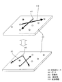
ここで、放射角φaの設定範囲は特にこだわらないが、例えば、360°全方向のブロードキャストと発光素子の放射角相当でなるべく小さな放射角の2種類を持つことが挙げられる。放射角は連続的に変更できるのがより好ましいが、不連続であってもよい。また、小さな放射角で放射する際には、放射方向を設定できるのが好ましい。すなわち、ポート102は拡散とビーム放射角の切替手段に加えて、ビームの方向設定手段の両方を持つことが好ましい。この様な通信方式により、1対1のポート間の組み合わせの切り替えだけでなく、図5に示すように、複数のポート間の伝達経路の切替、すなわち光回路の再構成が可能となる。
【0034】
一般に、光伝送シート101の任意の位置に光デバイスを配置しようとすると、伝播距離に応じて受光強度が異なってしまうので、信号伝達の信頼性を落としてしまうが、本通信方式は任意の位置に光デバイスを配置した場合にも有効である。また、電子回路と光回路が共存する上記回路基板とそれに適した上記通信方法は、電磁放射ノイズに強く設計自由度が高い柔軟な回路の再構成と、大量な情報を高速に扱うことを可能にする。
【0035】
また、光回路に2D導波路すなわち光伝送シートを適用することにより、上述の通信方法が実現でき、更に、従来の線状導波路とは異なり、所望の任意位置への光デバイス(発光素子や受光素子)の実装が可能となり、任意の位置の間での情報伝達が可能となる。光学的な位置合わせが比較的容易に光デバイスと導波路層の光結合を行える作用・効果もある。更に、単純な構成であるため簡易に回路基板を形成でき、薄型で高密度に実装がなされた回路基板を低コストで実現できる。
【0036】
(実施例2)
実施例2は、実施例1で述べた回路基板を用いて、別の通信方法を適用した例である。図2の基板上に実装されたLSI107aからLSI107bへデータ転送する場合を考える。この場合、LSI107は、2つのCPUないしはCPUとRAM等を想定している。
【0037】
まず、LSI107aが、発信用のポート102、例えば図3のポートEを指定する。通常、最近傍のポート(図2では102a)であるが、1つに固定されるものではない。1つの電子デバイス107に固有のポート102を予め決めておくのではなく、光配線接続の要求が発生するたび毎に、ポート102を指定する。この結果、光配線するデバイス107の数よりもずっと少ない数のポート102を準備しておけば良いことになる。
【0038】
図7に、本実施例のポート102間の光による通信方法のフローチャートの一例を示す。
3-1)ポートE(発信ポート)から通信要求信号を第1の放射角(広角)で発信する。
3-2)通信要求信号を受信したポートHが受信可能信号をポートEに返信する。
3-3)発信ポートEから受信ポートHに向けて第2の放射角(狭角)でデータを送信する。
すなわち、3-1)及び3-2)によりポートEとポートHの間で通信経路の確立がなされ、3-3)でデータ伝送が行われる。
【0039】
以下に、より詳しく説明する。
まず、3-1)において、ポートE(発信ポート)から通信要求信号を放射角360°で発信する。これには、図4における206xの発光素子を用いることで、2D光導波路101の全方向への発信がなされる。通信要求信号には、ポートEのアドレス、送りたい情報の容量、送りたいLSI107のアドレスなどの情報を持たせることができる。ここでは、通信要求信号の容量は256バイト、信号転送速度は100kbpsを用いた。
【0040】
3-2)において、通信要求信号を受信したポートHは、受信可能な際のみ、受信可能信号を返信する。受信可能であるかどうかは、現在、他のポート102と通信を行っているかどうか、受信したデータを格納する空きメモリを近傍に所有するか、などを判断材料として決定することが挙げられる。受信可能信号には、ポートHのアドレスなどが含まれる。この返信の際に用いる放射角は、ポートEが受信できるものであれば特にこだわらないが、広い放射角であれば、放射方向を設定する必要がないという利点があり好ましい。ポートEとポートHを結ぶ電気配線の経路がある場合は、電気配線を用いて返信しても良い。本実施例では、360°の放射角で光による情報伝達を用いた。受信可能信号の容量は256バイト、信号転送速度は100kbpsである。ここで、ポートHのほかにも、受信可能なポートは全てが返信を行なう。
【0041】
3-3)において、受信可能信号を受信したポートEは、受信ポートHの方向に第2の放射角でデータを伝送する。この際、複数のポート102から受信可能信号を受信した際には、その中から、最も好ましいポートを選ぶことができる。例えば、最終的に送りたいLSI107bに最も近いポート102を選ぶことが挙げられる。他にも、返信が早かったポートを選ぶことや、予めの優先順位として順位の高い方向のポートを選ぶことなどが挙げられる。本実施例では、データ伝送における第2の放射角としては90°を用いた。より具体的には、図4に示す様な光出力部において、発光部としてその中の1つ(例えば206c)を選んで動作させることで、2D光導波路101の所望の方向(ここではポートHの方向)への伝播を実現する。データ伝送の通信速度50Mbpsとした。第2の放射角が第1の放射角に比べて小さいので、高速な信号を扱える。ここではデータの送信先は1つのポート102としたが、複数のポートに同時に転送を行ってもよい。
【0042】
発信ポートEが、或る設定時間の間に、受信可能信号を受信できなかった場合には、再度、通信要求信号を送信する、すなわち3-1)に戻るようにしてもよい。以上のステップによりLSI107aからポートEを経てポートHで受信されたデータは、電気配線によりLSI107bに伝送される。
【0043】
この様な手法により、LSI107間の配線を任意に切り替えることができる。すなわち、回路の再構成が可能である。例えば、ポートEからポートHへとデータを送る回路から、引き続き、ポートCからポートDとFにデータを送る回路へと変更するなどの回路変更を行える。
【0044】
本実施例によれば、回路の切り替えを比較的短時間で実現できると共に、確実なデータ伝送が可能である。また、通信経路確立においては、大きな放射角領域を用い、遅い通信速度で伝送するため、広い領域に渡って情報の伝送が可能である。他方、本来目的とするデータ伝送においては、小さな放射角領域なので、十分な光量を受信ポートに伝送でき、高速で信頼性の高い伝送を行える。こうした手法により、適宜、最適な放射角領域を選ぶことで、情報通信に用いるエネルギーを有効に利用できる効果(消費電力の低減効果)も奏される。
【0045】
(実施例3)
実施例3の回路基板においては、ポート102には2つの発光素子を設け、1つの発光素子に対しては360°全方向への伝播が可能なように円錐ミラーの光結合部を配置し、もう1つの発光素子に対する光結合部としては、可動ミラーを配置した。ミラーを用いた際の放射角は10度であり、ミラーを動かすことで2D光導波路101における伝播方向を任意の方向に設定できる。他の構成は、実施例1に準じている。
【0046】
本実施例は、実施例2に比べて、より高度な通信方式を用い、信頼性の高い情報伝達を行なう例である。本実施例の通信方法を図8のフローチャート図を用いて説明する。
【0047】
4-1)はじめに、発信を行なうポート(例えば図3のポートB)は、媒体すなわち2D光導波路101が利用可能であるかを判断する。これには、例えば、ポートBの受光素子に検知される光強度が或る一定の強度以下であれば、利用可能とする。或る閾値より大きな光強度が検知された場合は、媒体が使用中であると判断し、発信を或る時間中止し、媒体が使用可能になるまで待機する。この様にすることで、例えば、光伝送媒体を占有して使うことができ、データ伝送の信頼性が高まる。
【0048】
4-2)次に、ポートB(発信ポート)から通信要求信号を第1の放射角(広角)で発信する。本実施例では、円錐ミラーの光結合部に対応した発光素子を動作させて360°の第1の放射角で発信を行なう。通信要求信号には、ポートBのアドレス、送りたい情報の容量、送りたいLSI107のアドレスなどの情報を持たせる。通信要求信号の容量は256バイト、信号転送速度は100kbpsを用いた。
【0049】
4-3)通信要求信号を受信したポート102のうちで、受信可能なポート(例えば、図3のポートC,G,I)が受信可能信号をポートBに返信する。このステップは、実施例2の3-2)のステップに準じる。
【0050】
4-4)受信可能信号を受信したポートBは、受信ポート先を選択し、経路指定信号を360°の放射角で発信する。経路指定信号にはポートBのアドレス、選択した受信ポートGのアドレスなどが含まれる。この返信の際には、ポートGが受信できる角度領域であれば放射角は特にこだわらないが、広い放射角であれば、放射方向を設定する必要がないという利点がある。ポートBとポートGを結ぶ電気配線の経路がある場合は、電気配線を用いて返信しても良い。本実施例では、360°の放射角の光による情報伝達を用いた。経路指定信号の容量は256バイト、信号転送速度は100kpbsである。
【0051】
4-5)経路指定信号を受信したポートGが、通信経路が確立したことを示すフラッグの経路確定信号をポートBに返信する。返信方法は特にこだわらないが、本実施例では、360°の放射角の光による情報伝達を用いた。
【0052】
4-6)経路確定信号を受信したポートBが、ポートGに向けて第2の放射角(狭角)でデータを送信する。本実施例では、ポートBからの光がポートGの方向に伝播するように、光結合部である可動ミラーを動かした。放射角は約10°である。データ伝送の通信速度は300Mbpsとした。放射角が小さいため、信頼性高く高速なデータを送信できる。
【0053】
4-7)引き続き、ポートBが送信終了信号をポートGに送信する。方法は特にこだわらないが、本実施例では、10°の放射角の光による情報伝達を用いた。
【0054】
4-8)最後に、ポートGがポートBに受信終了信号を返信する。返信方法は特にこだわらないが、本実施例では、360°の放射角の光による情報伝達を用いた。
【0055】
途中で返信等がなされなかった場合などは、エラーとなり、再度、最初のステップから信号伝達を行なうようになっている。また、受信可能信号を返信してから、或る時間の間に受信できたデータのみを正しい信号として認識するようにして、より回路の信頼性を高めることもできる。
【0056】
本実施例は、回路の切り替えを十分に短時間で実現できると共に、実施例2に比べて4-1),4),5),7),8)のステップを追加することで、より信頼性が高い伝達方法となっている。本実施例でも、通信経路確立においては、大きな放射角を用い、遅い通信速度で伝送するため、広い領域で情報の伝送が可能である一方で、データ伝送では、小さな放射角なので、十分な光量を受信ポートに伝送でき、高速で信頼性の高い伝送を行える。本実施例の手法は、実施例2の通信手法よりも、可動ミラーを用いた光結合により更に放射角を小さく設定できるため、より高速で信頼性の高い通信が可能である。その他の点は上記実施例と同じである。
【0057】
(実施例4)
実施例4においては、回路基板は実施例2と同様なものを用いた。ただし、各ポートは12kバイトのメモリを有している。本実施例は、実施例2に比べて、より高度な通信方式を用い、信頼性の高い情報伝達を行なう例である。本実施例の通信方法を図9のフローチャート図を用いて説明する。
【0058】
5-1)システムが起動すると、受信可能なポート(例えば図3のポートA,B,C,,,)は、定期的に受信待ち信号を発信する。例えば、50msおきに、自ポートのアドレスと受信待ちフラッグが記された受信待ち信号を360°の放射角で発信するようにしておく。この際、各ポート102から発信する時刻が異なるように予めタイミングを設定することで、混信を確実に防げる。受信待ち信号の容量は128バイト、信号転送速度は100kbpsを用いた。
【0059】
5-2)発信を行なうポート(例えば図3のポートE)は、受信ポートからの信号を読み取り、受信可能なポートの情報を獲得する。例えば、100ms間情報を蓄積し、受信待ち信号をメモリに保管する。
【0060】
5-3)発信ポートEは、受信可能なポートのうち、好ましいポート(例えばポートBとH)を選択し、通信要求信号を放射角360°で発信する。通信要求信号には、発信ポートEのアドレス、受信ポートB,Hのアドレス、送りたい情報の容量などの情報を持たせる。通信要求信号の容量256バイト、信号転送速度100kbpsを用いた。
【0061】
5-4)通信要求信号を受信したポートA,B,C,,,は、受信待ち信号の発信を停止する。これにより、後のデータ伝送においてデータの信頼性を高めることができる。
【0062】
5-5)通信要求信号を受信したポート102の中で、受信を行なうポート(ポートB,H)が受信可能信号をポートEに返信する。このステップは上記3-2)に準じる。
【0063】
5-6)ポートEから、ポートBとHに向けて、それぞれ第2の放射角(狭角)、ここでは90°の放射角でデータを送信する。このステップは上記3-3)に準じる。
【0064】
5-7)引き続き、ポートEが送信終了信号を発信する。発信には放射角360°の光による情報伝達を用いた。
【0065】
5-8)ポートBとポートHが受信終了信号を発信する。発信には放射角360°の光による情報伝達を用いた。
【0066】
5-9)送信終了信号、受信終了信号を受信した全てのポート102は、受信待ち信号の定期的な発信を再開する。すなわち、これにより通信経路の開放がなされたことになる。
【0067】
上記の伝達方法で、途中で返信等がなされなかった場合などには、エラーとなり、再度、信号伝達を行なうようになっている。本実施例でも、回路の切り替えを十分に短時間で実現できると共に、実施例2に比べて5-1),2),4),5),7),8),9)のステップを追加することで、より信頼性が高い手法となっている。
【0068】
本実施例の手法は、実施例2の通信手法よりも、可動ミラーを用いた光結合により更に放射角を小さく設定できるため、より高速で信頼性の高い通信が可能となっている。上述の手法、手続きは一例であり、これらに新たな手続きを追加することで、更に信頼性を高めても良い。ただし、手続きを増やすとそれだけ通信経路確立に時間がかかるため、システムの安定性に鑑みて、適当な手法に設計するのが良い。その他の点は上記実施例と同じである。
【0069】
上記の各実施例において、光信号を発信もしくは受信する機能を有したポートの間で柔軟に光回路を形成できる情報伝達方法は、ポート間で通信経路の確立を行なう第1のステップと、引き続き、該通信経路を用いてデータ伝送を行なう第2のステップを有して所期の情報伝達を行なう情報伝達方法であって、第1のステップにおいてポートから放出される光の第1の放射角領域が、第2のステップにおいてポートから放出される光の第2の放射角領域を含んでこれよりも大きかったが、第1の放射角領域と第2の放射角領域が一部重なっている様な態様、第2の放射角領域が第1の放射角領域を含んで大きい様な態様なども可能である。こうした態様を必要とする場合としては、例えば、第1のステップでポート間の所望のデータ伝送を行なって、第2のステップで適当な情報を含んだ信号を伝送して後確認(例えば、データを伝送した受信ポートの周りのポートに該伝送の完了を知らせる)を行なう例などがある。つまり、各ステップでどの様な情報内容の光伝送を行なうかは、利用する通信プロトコル、伝送目的などに応じて様々であり、その光伝送の内容(例えば、データ信号そのものであるか、制御信号(通信要求信号、確認信号、エラー訂正信号、アドレス信号、割込み信号等)であるかなど)に応じて各ステップの放射角領域を設定すればよい。
【0070】
【発明の効果】
以上に説明した如くに、本発明により、発信ポートと受信ポートを備えた光回路、光回路装置において柔軟に光回路を形成して所期の情報伝達を行なえる情報伝達方法を実現できる。
【図面の簡単な説明】
【図1】図1は2D光導波路の放射角を示す図である。
【図2】図2は電子回路、光回路を積層した回路基板である。
【図3】図3はポート配置例を示す図である。
【図4】図4は光結合部の構成例を示す図である。
【図5】図5は光回路の再構成を示す図である。
【図6】図6は本発明の実施例1の通信方式を示すフローチャート図である。
【図7】図7は本発明の実施例2の通信方式を示すフローチャート図である。
【図8】図8は本発明の実施例3の通信方式を示すフローチャート図である。
【図9】図9は本発明の実施例4の通信方式を示すフローチャート図である。
【符号の説明】
100 基板
101 光伝送シート(2D導波路)
102 光ポート
103 伝播光
104 放射角
105 電気配線層
106 電気配線
107 電子デバイス(LSI等)
110 伝達経路
201 光結合部
202 光照射位置
203 発光部からの光
204 伝播光
205 光出力部
206 発光部[0001]
BACKGROUND OF THE INVENTION
The present invention relates to information transmission in which information is transmitted by light through an optical transmission medium between a transmission port having a function of transmitting an optical signal and a reception port having a function of receiving an optical signal.MethodIn particular, information transmission that transmits information by forming an optical circuit flexibly between the transmission port and the reception portMethodAbout.
[0002]
[Prior art]
Recently, in addition to high processing speed and small size / light weight, information processing devices such as personal computers and mobile phones and personal information terminals (PDAs) are desired to switch between multiple applications. ing. On the other hand, in a control device such as a robot, it is desired to control by switching a plurality of control algorithms in real time. From such a viewpoint, a circuit board capable of reconfiguring a circuit, particularly a circuit board capable of reconfiguring a circuit at high speed in real time is desired.
[0003]
Conventionally, it has been common to try to realize such a circuit with electronic circuits, switches, memories, etc. However, as processing speed increases, problems such as wiring delay and EMI (electromagnetic radiation interference noise) occur. . As a technique for avoiding such wiring delay and EMI, it is possible to use an optical wiring capable of high-speed transmission and having the advantage of electromagnetic non-induction (see, for example, Patent Document 1).
[0004]
[Patent Document 1]
JP-A-5-67770
[0005]
[Problems to be solved by the invention]
However, the optical wiring method described in Patent Document 1 and the like described above has insufficient flexibility in forming the optical wiring.
[0006]
In view of the above problems, an object of the present invention is to provide information transmission in which an optical circuit can be flexibly formed between a transmission port and a reception port in an optical circuit device having a transmission port and a reception port.MethodIs to provide.
[0007]
[Means for Solving the Problems]
To achieve the above object, the present inventionFirstAn information transmission method includes a transmission port having a function of transmitting an optical signal and a plurality of reception ports having a function of receiving an optical signal.And optical transmission sheet that propagates optical signalsBetween the transmission port and the reception port in an optical circuit device equipped withOptical transmission sheetIs an information transmission method for transmitting information via an outgoing port.In the light transmission sheetEmit light in the first radiation angle region and at leastTwoA first step of transmitting first information to a receiving port; and after the first step, the first radiation angle region from the transmitting portNarrowerBy a transmission comprising a second step of emitting light in a second radiation angle region and transmitting a second information to at least one receiving port;The second 1 The second step and the second step togetherIt is characterized by information transmission.In addition, the second information transmission method of the present invention that achieves the above object provides a transmission port having a function of transmitting an optical signal, a plurality of reception ports having a function of receiving an optical signal, and an optical signal that propagates the optical signal. An information transmission method for transmitting information between a transmission port and a reception port via an optical transmission sheet in an optical circuit device having a transmission sheet, wherein light is transmitted from the transmission port into the optical transmission sheet in a first radiation angle region. A first step of transmitting first information to one receiving port and a second radiation greater than the first radiation angle region from the transmission port after the first step A transmission including a second step of emitting light in a corner region and transmitting second information to a plurality of receiving ports, 1 The step 2 and the second step are characterized by jointly transmitting the desired information.. Since this information transmission method uses a plurality of steps of emitting light from the transmission port in different emission angle regions, an optical circuit is flexibly formed between the transmission port and the reception port to transmit an optical signal. Can communicate information. What kind of information content is optically transmitted in each step is variously determined according to the communication protocol to be used, the purpose of transmission, and the like. In each step, the reception port that can be received is determined by the radiation angle area of the light from the transmission port, but it is not necessary for all reception ports that can be received, and whether or not to receive is determined on the reception port side. May be.
[0008]
In the basic information transmission method, a communication path is established between the transmission port and at least one reception port in the first step, and subsequently, data transmission is performed using the communication path in the second step. The radiation angle region of the light emitted from the transmission port in the first step can be made larger than the radiation angle region emitted from the transmission port in the second step. Further, the data transfer rate in the first step can be made slower than the data transfer rate in the second step, so that information can be transmitted reliably and efficiently.
[0009]
In addition, at least through the following procedures, it is possible to reliably transmit information by light,
1) Communication request signal from port A in the first radiation angle regionTo multiple portsOutgoing,
2) Received a communication request signalOf the multiple portsPort B returns a signal that can be received to Port A,
3) Data is transmitted from port A to port B in a second radiation angle region that is smaller than the first radiation angle region.
[0010]
Further, the receivable signal may be transmitted using electrical wiring, or the number of ports receiving information in the first step may be larger than the number of ports receiving information in the second step. It can also be.
[0013]
DETAILED DESCRIPTION OF THE INVENTION
Embodiments of the present invention will be described below with specific examples. However, the present invention is not limited to the embodiments described below, and any specific configuration may be used as long as it is included in the basic configuration concept described above.
[0014]
Example 1
The circuit board according to the first embodiment of the present invention is a circuit board in which an optical circuit and an electronic circuit are mixed so that information can be transmitted by light between optical ports having a function of transmitting or receiving an optical signal. It is configured. The light output part of the transmission port for transmitting information has means for propagating light in a two-dimensional (2D) optical waveguide (light transmission sheet) by switching from two or more types of radiation angle regions to a desired radiation angle region. This switching means realizes information transmission by light between ports. FIG. 1 shows examples of different
[0015]
FIG. 2 is a schematic cross-sectional view illustrating a circuit board according to the first embodiment. In the circuit board structure example of FIG. 2, 100 is the entire substrate, 101 is a light transmission sheet that is a 2D optical waveguide, and 102 is a light input (reception) provided near the interface between the
[0016]
In the configuration example of FIG. 2, the
[0017]
As shown in FIG. 2, in the circuit board in this embodiment, an electronic circuit having an electronic device 107 and an
[0018]
Hereinafter, each element will be described in more detail.
In this example, as the
[0019]
The
[0020]
An electrical signal of an LSI or the like that is the electronic device 107 can be transmitted as an optical signal via the
[0021]
The
[0022]
The light output portion of the
[0023]
A logic signal (for example, 3.3 V in the case of CMOS) of the electronic device 107 such as an LSI has a voltage sufficient to drive the light emitting element of the
[0024]
The light emitted from the light emitting element propagates through the
[0025]
As described above, in this embodiment, the radiation angle can be switched by arranging a plurality of light emitting elements in the
[0026]
Furthermore, as a light-emitting element that can be applied to the light output unit, there is a device that can control and change a radiation angle by controlling an injection current or the like. A method of changing the radiation angle is also possible by changing the coupling mode between the light emitting element of the light output unit and the 2D optical waveguide. More specifically, the optical coupling part such as mirrors, prisms, lenses, and gratings arranged close to the light emitting element is moved, the position of the light emitting element itself is moved to give the effect of changing the radiation angle, or the optical coupling is performed. Similar effects can be achieved by modulating the optical properties such as the refractive index of the material constituting the part. For example, there is a method of forming a minute movable mirror or the like by applying an electrostatic force, a magnetic force, a piezoelectric element, or the like by micromechanics technology. As an optical coupler applied to the light output unit, a lens, a prism, a mirror, a grating, and the like are preferable because light from the light emitting element can be emitted to the 2D waveguide at a predetermined radiation angle. In particular, typical examples of light that can be emitted to the 2D waveguide at a predetermined radiation angle include a cone shape, a pyramid shape, and a spherical mirror. Of course, the means for switching the radiation angle region is not limited to these, and any means can be applied.
[0027]
The optical signal propagating through the
[0028]
Moreover, what received the some light-receiving part in the array form can also be used as a receiving port. In particular, the light receiving portions may be arranged so that the incident directions to the respective light receiving portions of the array are different. By selecting the light receiving unit used in the array, it is possible to sort and select the direction of the reaching light.
[0029]
When the electronic device and the optical device in this example were operated, it was confirmed that an optical circuit was formed between the ports and a desired operation was performed. That is, it was confirmed that the optical circuit having means for switching the radiation angle region or the radiation direction appropriately works depending on the communication contents. Such a circuit board is a circuit board having a high degree of freedom of wiring having an optical wiring circuit capable of forming wiring flexibly in addition to an electronic circuit. In such a configuration, by executing a communication method described later, high-speed communication can be realized over a relatively long distance in the 2D optical waveguide.
[0030]
Hereinafter, an example of a method for transmitting information using the above configuration will be described.
In the information transmission by light between the ports in the present embodiment, it is possible to execute a method in which a desired information transmission is performed including a step of establishing a communication path and a step of subsequently performing data transmission using the communication path. . Since the 2D
[0031]
This point will be described in detail. In information transmission using a 2D optical waveguide, when light is propagated at a radiation angle φa, the light at the receiving site is proportional to L / (Rφa) (L: size of light input section, R: distance). Strength will be reduced. Also, when propagating at a large radiation angle, light is wasted except in the direction in which reception is performed. On the other hand, in data transmission, when the reception strength is reduced, the error rate and the data transfer rate are limited from the viewpoint of S / N. From this point of view, it is better to make the radiation angle as small as possible for high-speed and reliable transmission. However, if the radiation angle is reduced, the number of parties that can communicate is reduced, and the degree of freedom of the circuit is reduced. In order to achieve both of these conflicting effects, the above-described communication method for switching the radiation angle region functions effectively. Thus, in establishing a communication path, it is preferable to propagate a signal having a low communication speed with a large radiation angle φa, and to perform data transmission at a high communication speed with a small radiation angle after establishing the path. In general, the amount of data required for establishing a communication path is small, and it is not the data transfer rate but rather the switching time of a physical circuit that determines the path establishment. For this reason, there is substantially no problem even if the data transfer speed in establishing the communication path is not so high. Also, if the data transfer rate is reduced in establishing a communication path, relatively reliable information transmission is possible even if the amount of light reaching the receiving port is small, and information transmission over a wider range is possible. On the other hand, since the amount of data related to desired information transmission is large, high-speed data transmission is desirable. Therefore, the proper use of the data transfer rate as described above can be said to be a preferable method in this communication method.
[0032]
Thus, by using the circuit and the optical circuit device, it is possible to realize an information transmission method capable of high-speed and high-reliability data transmission by sharing the optical transmission medium with high wiring flexibility. In this method, since the use of light energy is eliminated by appropriately selecting the radiation angle region or the radiation direction, there is an effect of reducing power consumption.
[0033]
Here, although the setting range of the radiation angle φa is not particularly limited, for example, there are two types of radiation angles that are as small as possible, which are broadcast in all directions of 360 ° and equivalent to the radiation angle of the light emitting element. More preferably, the radiation angle can be changed continuously, but it may be discontinuous. Moreover, when radiating with a small radiation angle, it is preferable that the radiation direction can be set. That is, the
[0034]
In general, if an optical device is arranged at an arbitrary position on the
[0035]
Further, by applying a 2D waveguide, that is, an optical transmission sheet, to the optical circuit, the above-described communication method can be realized. Further, unlike a conventional linear waveguide, an optical device (light emitting element or Light receiving element) can be mounted, and information can be transmitted between arbitrary positions. There is also a function and an effect that optical alignment between the optical device and the waveguide layer can be performed relatively easily. Furthermore, since it has a simple configuration, a circuit board can be easily formed, and a thin and high-density circuit board can be realized at low cost.
[0036]
(Example 2)
The second embodiment is an example in which another communication method is applied using the circuit board described in the first embodiment. Consider a case where data is transferred from the
[0037]
First, the
[0038]
FIG. 7 shows an example of a flowchart of a communication method using light between the
3-1) A communication request signal is transmitted from the port E (transmission port) at the first radiation angle (wide angle).
3-2) Port H that has received the communication request signal returns a receivable signal to port E.
3-3) Data is transmitted from the transmission port E to the reception port H at the second radiation angle (narrow angle).
That is, a communication path is established between port E and port H by 3-1) and 3-2), and data transmission is performed by 3-3).
[0039]
This will be described in more detail below.
First, in 3-1), a communication request signal is transmitted from the port E (transmission port) at a radiation angle of 360 °. For this purpose, transmission in all directions of the 2D
[0040]
In 3-2), the port H that has received the communication request signal returns a receivable signal only when reception is possible. Whether or not the data can be received includes determining whether or not communication is currently being performed with another
[0041]
In 3-3), the port E that has received the receivable signal transmits data in the direction of the reception port H at the second radiation angle. At this time, when receivable signals are received from a plurality of
[0042]
If the transmission port E fails to receive a receivable signal for a certain set time, it may transmit the communication request signal again, that is, return to 3-1). Data received at port H from
[0043]
With such a method, the wiring between the LSIs 107 can be arbitrarily switched. That is, the circuit can be reconfigured. For example, it is possible to change the circuit such as changing the circuit that sends data from port E to port H to the circuit that sends data from port C to ports D and F.
[0044]
According to this embodiment, circuit switching can be realized in a relatively short time, and reliable data transmission is possible. In establishing a communication path, a large radiation angle region is used and transmission is performed at a low communication speed, so that information can be transmitted over a wide region. On the other hand, since the intended data transmission is a small radiation angle region, a sufficient amount of light can be transmitted to the receiving port, and high-speed and highly reliable transmission can be performed. By appropriately selecting the optimum radiation angle region by such a method, an effect of effectively using energy used for information communication (an effect of reducing power consumption) is also exhibited.
[0045]
(Example 3)
In the circuit board of Example 3, the
[0046]
The present embodiment is an example of performing highly reliable information transmission using a more advanced communication method than the second embodiment. The communication method of the present embodiment will be described with reference to the flowchart of FIG.
[0047]
4-1) First, a transmission port (for example, port B in FIG. 3) determines whether the medium, that is, the 2D
[0048]
4-2) Next, a communication request signal is transmitted from port B (transmission port) at the first radiation angle (wide angle). In this embodiment, the light emitting element corresponding to the optical coupling part of the conical mirror is operated to perform transmission at a first radiation angle of 360 °. The communication request signal includes information such as the port B address, the capacity of information to be sent, and the address of the LSI 107 to be sent. The capacity of the communication request signal was 256 bytes, and the signal transfer rate was 100 kbps.
[0049]
4-3) Among the
[0050]
4-4) Port B that has received the receivable signal selects the receiving port destination and sends the routing signal at a 360 ° radiation angle. The routing signal includes the port B address, the selected receiving port G address, and the like. At the time of this reply, the radiation angle is not particularly limited if it is an angle region that can be received by the port G, but if it is a wide radiation angle, there is an advantage that it is not necessary to set the radiation direction. If there is an electrical wiring path connecting port B and port G, a reply may be made using the electrical wiring. In this example, information transmission using light having a radiation angle of 360 ° was used. The capacity of the routing signal is 256 bytes and the signal transfer rate is 100 kpbs.
[0051]
4-5) Port G that has received the routing signal returns a flag route confirmation signal indicating that the communication route has been established, to port B. The reply method is not particularly limited, but in this embodiment, information transmission using light with a radiation angle of 360 ° was used.
[0052]
4-6) Port B that has received the route determination signal transmits data to port G at the second radiation angle (narrow angle). In this embodiment, the movable mirror that is the optical coupling portion is moved so that the light from the port B propagates in the direction of the port G. The radiation angle is about 10 °. The communication speed for data transmission was 300 Mbps. Since the radiation angle is small, it is possible to transmit data with high reliability and high speed.
[0053]
4-7) Subsequently, port B transmits a transmission end signal to port G. Although the method is not particularly limited, in this embodiment, information transmission using light having a radiation angle of 10 ° was used.
[0054]
4-8) Finally, port G returns a reception end signal to port B. The reply method is not particularly limited, but in this embodiment, information transmission using light with a radiation angle of 360 ° was used.
[0055]
If no reply is made on the way, an error occurs and signal transmission is performed again from the first step. In addition, it is possible to further improve the reliability of the circuit by recognizing only data that can be received within a certain period of time after returning a receivable signal as a correct signal.
[0056]
In this embodiment, circuit switching can be realized in a sufficiently short time, and more reliable by adding steps 4-1), 4), 5), 7), and 8) than in the second embodiment. It has become a highly reliable transmission method. Even in this embodiment, when a communication path is established, since a large radiation angle is used and transmission is performed at a low communication speed, information can be transmitted over a wide area. Can be transmitted to the receiving port, and high-speed and reliable transmission can be performed. In the method of the present embodiment, the radiation angle can be set smaller than that of the communication method of the second embodiment by optical coupling using a movable mirror, so that higher-speed and highly reliable communication is possible. The other points are the same as the above embodiment.
[0057]
(Example 4)
In Example 4, the same circuit board as in Example 2 was used. However, each port has a 12 kbyte memory. The present embodiment is an example of performing highly reliable information transmission using a more advanced communication method than the second embodiment. The communication method of the present embodiment will be described with reference to the flowchart of FIG.
[0058]
5-1) When the system is activated, the receivable ports (for example, ports A, B, C,... In FIG. 3) periodically transmit a reception waiting signal. For example, every 50 ms, a reception waiting signal in which the address of the own port and a reception waiting flag are written is transmitted at a 360 ° emission angle. At this time, interference is reliably prevented by setting the timing in advance so that the time of transmission from each
[0059]
5-2) A port that performs transmission (for example, port E in FIG. 3) reads a signal from the reception port and acquires information on a port that can be received. For example, information is accumulated for 100 ms, and a reception waiting signal is stored in a memory.
[0060]
5-3) Outgoing port E selects a preferable port (for example, ports B and H) out of receivable ports, and sends a communication request signal at a radiation angle of 360 °. The communication request signal has information such as the address of the transmission port E, the addresses of the reception ports B and H, and the capacity of information to be sent. A communication request signal capacity of 256 bytes and a signal transfer rate of 100 kbps were used.
[0061]
5-4) The ports A, B, C,... That have received the communication request signal stop transmitting the reception waiting signal. Thereby, the reliability of data can be improved in subsequent data transmission.
[0062]
5-5) Of the
[0063]
5-6) Data is transmitted from port E toward ports B and H at a second radiation angle (narrow angle), here a radiation angle of 90 °. This step conforms to 3-3) above.
[0064]
5-7) Subsequently, port E sends a transmission end signal. Information transmission using light with a radiation angle of 360 ° was used for transmission.
[0065]
5-8) Port B and port H send a reception end signal. Information transmission using light with a radiation angle of 360 ° was used for transmission.
[0066]
5-9) All the
[0067]
If a reply is not made in the above transmission method, an error occurs and the signal is transmitted again. In this embodiment, circuit switching can be realized in a sufficiently short time, and steps 5-1), 2), 4), 5), 7), 8), 9) are added compared to the second embodiment. By doing so, the method is more reliable.
[0068]
In the method of the present embodiment, since the radiation angle can be set smaller than that of the communication method of the second embodiment by optical coupling using a movable mirror, communication at higher speed and higher reliability is possible. The above-described methods and procedures are examples, and reliability may be further improved by adding new procedures to them. However, as the number of procedures increases, it takes time to establish a communication path. Therefore, it is better to design an appropriate method in view of the stability of the system. The other points are the same as the above embodiment.
[0069]
In each of the above-described embodiments, an information transmission method capable of forming an optical circuit flexibly between ports having a function of transmitting or receiving an optical signal includes a first step of establishing a communication path between the ports, An information transmission method for performing desired information transmission having a second step of performing data transmission using the communication path, wherein the first emission angle of light emitted from the port in the first step The area was larger than the second emission angle area of the light emitted from the port in the second step, but the first emission angle area and the second emission angle area partially overlapped. Such a mode, a mode in which the second radiation angle region is large including the first radiation angle region, and the like are also possible. When such a mode is required, for example, desired data transmission between ports is performed in the first step, and a signal including appropriate information is transmitted in the second step and then confirmed (for example, data For example, performing notification of the completion of the transmission to the ports around the receiving port that transmitted. In other words, what kind of information content is optically transmitted in each step varies depending on the communication protocol to be used, the purpose of transmission, etc., and the content of the optical transmission (for example, whether it is a data signal itself, The radiation angle region of each step may be set according to (communication request signal, confirmation signal, error correction signal, address signal, interrupt signal, etc.).
[0070]
【The invention's effect】
As described above, according to the present invention, information transmission that can flexibly form an optical circuit in an optical circuit and an optical circuit device having a transmission port and a reception port to perform intended information transmission.MethodCan be realized.
[Brief description of the drawings]
FIG. 1 is a diagram showing a radiation angle of a 2D optical waveguide.
FIG. 2 is a circuit board on which electronic circuits and optical circuits are stacked.
FIG. 3 is a diagram illustrating a port arrangement example;
FIG. 4 is a diagram illustrating a configuration example of an optical coupling unit.
FIG. 5 is a diagram showing a reconfiguration of an optical circuit.
FIG. 6 is a flowchart showing a communication system according to the first embodiment of the present invention.
FIG. 7 is a flowchart showing a communication method according to the second embodiment of the present invention.
FIG. 8 is a flowchart showing a communication system according to a third embodiment of the present invention.
FIG. 9 is a flowchart illustrating a communication method according to a fourth embodiment of this invention.
[Explanation of symbols]
100 substrates
101 Optical transmission sheet (2D waveguide)
102 optical port
103 Propagating light
104 Radiation angle
105 Electrical wiring layer
106 Electrical wiring
107 Electronic devices (LSI, etc.)
110 Transmission path
201 Optical coupling
202 Light irradiation position
203 Light from the light emitting section
204 Propagating light
205 Optical output section
206 Light emitter
Claims (5)
発信ポートから光伝送シート内に第1の放射角領域で光を放出して少なくとも2つの受信ポートに対して第1の情報伝達を行なう第1のステップと、該第1のステップの後で、該発信ポートから該第1の放射角領域より狭い第2の放射角領域で光を放出して少なくとも1つの受信ポートに対して第2の情報伝達を行なう第2のステップを含む伝送により、第 1 のステップと第2のステップは共同して所期の情報伝達を行なうことを特徴とする情報伝達方法。 Light between the originating port and the receiving port in an optical circuit device having the optical sheet propagating a plurality of receive ports and an optical signal having a function of receiving an outgoing port and an optical signal having a function of transmitting an optical signal An information transmission method for transmitting information via a transmission sheet ,
A first step of emitting light in a first radiation angle region from a transmission port into a light transmission sheet to transmit first information to at least two reception ports; and after the first step, A transmission comprising a second step of emitting light from the transmission port in a second radiation angle region narrower than the first radiation angle region to deliver second information to at least one reception port ; An information transmission method characterized in that the first step and the second step jointly perform intended information transmission.
発信ポートから光伝送シート内に第1の放射角領域で光を放出して1つの受信ポートに対して第1の情報伝達を行なう第1のステップと、該第1のステップの後で、該発信ポートから該第1の放射角領域より大きい第2の放射角領域で光を放出して複数の受信ポートに対して第2の情報伝達を行なう第2のステップを含む伝送により、第 1 のステップと第2のステップは共同して所期の情報伝達を行なうことを特徴とする情報伝達方法。 In an optical circuit device provided with a transmission port having a function of transmitting an optical signal, a plurality of reception ports having a function of receiving an optical signal, and an optical transmission sheet for propagating the optical signal, light is transmitted between the transmission port and the reception port. An information transmission method for transmitting information via a transmission sheet,
A first step of emitting light in a first radiation angle region from a transmission port into a light transmission sheet to transmit a first information to one reception port; and after the first step, the transmission from the calling port including the second step of emitting light in a larger first emission angle region second emission angle region performs second signaling to a plurality of receiving ports, a first An information transmission method characterized in that the step and the second step jointly perform intended information transmission.
1)ポートAから通信要求信号を第1の放射角領域で複数のポートへ発信、
2)通信要求信号を受信した複数のポートのうち、ポートBが受信可能信号をポートAに返信、
3)ポートAからポートBに向けて第1の放射角領域より小さい第2の放射角領域でデータを送信。At least through the following procedure, the method of information transmission according to claim 1, wherein performing the information transmission by light,
1) A communication request signal is transmitted from port A to a plurality of ports in the first radiation angle region.
2) Of the plurality of ports that have received the communication request signal , port B returns a receivable signal to port A,
3) Data is transmitted from port A to port B in a second radiation angle region that is smaller than the first radiation angle region.
Priority Applications (4)
| Application Number | Priority Date | Filing Date | Title |
|---|---|---|---|
| JP2003000017A JP3913175B2 (en) | 2003-01-06 | 2003-01-06 | Information transmission method in optical circuit device |
| US10/533,564 US7257282B2 (en) | 2003-01-06 | 2003-12-25 | Process of information transmission in optical circuit device and optical circuit device therefor |
| PCT/JP2003/016706 WO2004062138A1 (en) | 2003-01-06 | 2003-12-25 | Process of information transmission in optical circuit device and optical circuit device therefor |
| AU2003295233A AU2003295233A1 (en) | 2003-01-06 | 2003-12-25 | Process of information transmission in optical circuit device and optical circuit device therefor |
Applications Claiming Priority (1)
| Application Number | Priority Date | Filing Date | Title |
|---|---|---|---|
| JP2003000017A JP3913175B2 (en) | 2003-01-06 | 2003-01-06 | Information transmission method in optical circuit device |
Publications (3)
| Publication Number | Publication Date |
|---|---|
| JP2004215000A JP2004215000A (en) | 2004-07-29 |
| JP2004215000A5 JP2004215000A5 (en) | 2006-01-26 |
| JP3913175B2 true JP3913175B2 (en) | 2007-05-09 |
Family
ID=32708755
Family Applications (1)
| Application Number | Title | Priority Date | Filing Date |
|---|---|---|---|
| JP2003000017A Expired - Fee Related JP3913175B2 (en) | 2003-01-06 | 2003-01-06 | Information transmission method in optical circuit device |
Country Status (4)
| Country | Link |
|---|---|
| US (1) | US7257282B2 (en) |
| JP (1) | JP3913175B2 (en) |
| AU (1) | AU2003295233A1 (en) |
| WO (1) | WO2004062138A1 (en) |
Families Citing this family (3)
| Publication number | Priority date | Publication date | Assignee | Title |
|---|---|---|---|---|
| JP4910448B2 (en) * | 2006-03-28 | 2012-04-04 | 富士通株式会社 | 3D circuit module |
| JP2010211179A (en) * | 2009-02-13 | 2010-09-24 | Hitachi Ltd | Photoelectric composite wiring module and method for manufacturing the same |
| JP5992652B1 (en) * | 2013-09-02 | 2016-09-14 | フィリップス ライティング ホールディング ビー ヴィ | Transparent computer structure |
Family Cites Families (11)
| Publication number | Priority date | Publication date | Assignee | Title |
|---|---|---|---|---|
| JPH0642527B2 (en) * | 1989-10-10 | 1994-06-01 | 日本電気株式会社 | Information processing device using optical waveguide |
| US5357122A (en) * | 1991-09-05 | 1994-10-18 | Sony Corporation | Three-dimensional optical-electronic integrated circuit device with raised sections |
| JPH05183515A (en) | 1991-12-27 | 1993-07-23 | Mitsubishi Electric Corp | Optical space transmitter |
| JP3064839B2 (en) | 1994-12-22 | 2000-07-12 | 松下電器産業株式会社 | Spatial light transmission device and light beam deflector |
| JP3230961B2 (en) | 1995-10-13 | 2001-11-19 | 株式会社エヌ・ティ・ティ・データ | Optical axis adjustment method of optical transceiver |
| JPH09307502A (en) | 1996-05-10 | 1997-11-28 | Fuji Xerox Co Ltd | Infrared ray communication equipment |
| JP3902883B2 (en) * | 1998-03-27 | 2007-04-11 | キヤノン株式会社 | Nanostructure and manufacturing method thereof |
| US6573984B2 (en) * | 1998-06-30 | 2003-06-03 | Lj Laboratories Llc | Apparatus and method for measuring optical characteristics of teeth |
| JP2000261383A (en) | 1999-03-11 | 2000-09-22 | Hittsu Kenkyusho:Kk | Optical radio transmitting device for multi-port satellite |
| JP2004317717A (en) | 2003-04-15 | 2004-11-11 | Canon Inc | Reconfigurable photoelectric fusion circuit |
| US7248757B2 (en) * | 2003-12-15 | 2007-07-24 | Canon Kabushiki Kaisha | Method, device and computer program for designing a circuit having electric wires and optical connections |
-
2003
- 2003-01-06 JP JP2003000017A patent/JP3913175B2/en not_active Expired - Fee Related
- 2003-12-25 WO PCT/JP2003/016706 patent/WO2004062138A1/en active Application Filing
- 2003-12-25 US US10/533,564 patent/US7257282B2/en not_active Expired - Fee Related
- 2003-12-25 AU AU2003295233A patent/AU2003295233A1/en not_active Abandoned
Also Published As
| Publication number | Publication date |
|---|---|
| AU2003295233A1 (en) | 2004-07-29 |
| WO2004062138A1 (en) | 2004-07-22 |
| US20060110093A1 (en) | 2006-05-25 |
| JP2004215000A (en) | 2004-07-29 |
| US7257282B2 (en) | 2007-08-14 |
Similar Documents
| Publication | Publication Date | Title |
|---|---|---|
| JP4095404B2 (en) | Optical connection device, opto-electric hybrid device, and electronic device using the same | |
| JP3848210B2 (en) | Electronic circuit board | |
| JP3833131B2 (en) | Optical transmission equipment | |
| TWI254153B (en) | Photonic circuit board | |
| US6721503B1 (en) | System and method for bi-directional optical communication using stacked emitters and detectors | |
| JP2003279771A (en) | Light guide device, photoelectric fusion substrate, high speed serial bus, and their manufacturing method | |
| US6928205B2 (en) | Optical waveguide device, layered substrate and electronics using the same | |
| US5073000A (en) | Optical interconnect printed circuit structure | |
| JP2004061799A (en) | Two-dimensional waveguide apparatus and opto-electronic fusion wiring board using same | |
| US7200293B2 (en) | Reconfigurable optoelectronic circuit | |
| JP5277874B2 (en) | Opto-electric hybrid board and electronic equipment | |
| JP2003057468A (en) | Optical element, optical waveguide device, their manufacturing method, and photoelectric hybrid substrate using them | |
| JP3913175B2 (en) | Information transmission method in optical circuit device | |
| US7653272B2 (en) | Highly parallel optical communication system with intracard and intercard communications | |
| JP2003227951A (en) | Optical waveguide device, method of manufacturing the same, and optoelectric coexisting substrate using the same | |
| JP2004320666A (en) | Optical transmission device, photoelectric fusion circuit in which electronic circuit and optical circuit are mixed | |
| JP4995867B2 (en) | Light emitting device and optical coupling module | |
| CN110855369A (en) | Externally-connected portable wireless optical communication assembly and method for small mobile electronic equipment | |
| US20040146238A1 (en) | Optical connector device, and optical and electrical circuit combined board using the same | |
| KR101629531B1 (en) | Photonic waveguide | |
| CN106526764A (en) | Optical structure applied to COB encapsulation | |
| JPS6356612A (en) | Optical wiring circuit unit | |
| JP4789423B2 (en) | Optical waveguide device | |
| JP2003029070A (en) | Opto-electric merged wiring substrate and optical wiring substrate | |
| JP2001091773A (en) | Optical circuit module |
Legal Events
| Date | Code | Title | Description |
|---|---|---|---|
| A521 | Request for written amendment filed |
Free format text: JAPANESE INTERMEDIATE CODE: A523 Effective date: 20051121 |
|
| A621 | Written request for application examination |
Free format text: JAPANESE INTERMEDIATE CODE: A621 Effective date: 20051121 |
|
| A131 | Notification of reasons for refusal |
Free format text: JAPANESE INTERMEDIATE CODE: A131 Effective date: 20060728 |
|
| A521 | Request for written amendment filed |
Free format text: JAPANESE INTERMEDIATE CODE: A523 Effective date: 20060920 |
|
| TRDD | Decision of grant or rejection written | ||
| A01 | Written decision to grant a patent or to grant a registration (utility model) |
Free format text: JAPANESE INTERMEDIATE CODE: A01 Effective date: 20070123 |
|
| A61 | First payment of annual fees (during grant procedure) |
Free format text: JAPANESE INTERMEDIATE CODE: A61 Effective date: 20070130 |
|
| R150 | Certificate of patent or registration of utility model |
Free format text: JAPANESE INTERMEDIATE CODE: R150 |
|
| FPAY | Renewal fee payment (event date is renewal date of database) |
Free format text: PAYMENT UNTIL: 20100209 Year of fee payment: 3 |
|
| FPAY | Renewal fee payment (event date is renewal date of database) |
Free format text: PAYMENT UNTIL: 20110209 Year of fee payment: 4 |
|
| FPAY | Renewal fee payment (event date is renewal date of database) |
Free format text: PAYMENT UNTIL: 20120209 Year of fee payment: 5 |
|
| FPAY | Renewal fee payment (event date is renewal date of database) |
Free format text: PAYMENT UNTIL: 20130209 Year of fee payment: 6 |
|
| FPAY | Renewal fee payment (event date is renewal date of database) |
Free format text: PAYMENT UNTIL: 20140209 Year of fee payment: 7 |
|
| LAPS | Cancellation because of no payment of annual fees |