JP2010199492A - Semiconductor device and method of manufacturing same - Google Patents
Semiconductor device and method of manufacturing same Download PDFInfo
- Publication number
- JP2010199492A JP2010199492A JP2009045570A JP2009045570A JP2010199492A JP 2010199492 A JP2010199492 A JP 2010199492A JP 2009045570 A JP2009045570 A JP 2009045570A JP 2009045570 A JP2009045570 A JP 2009045570A JP 2010199492 A JP2010199492 A JP 2010199492A
- Authority
- JP
- Japan
- Prior art keywords
- island
- lead
- wire
- semiconductor device
- metal
- Prior art date
- Legal status (The legal status is an assumption and is not a legal conclusion. Google has not performed a legal analysis and makes no representation as to the accuracy of the status listed.)
- Pending
Links
Images


Classifications
-
- H—ELECTRICITY
- H01—ELECTRIC ELEMENTS
- H01L—SEMICONDUCTOR DEVICES NOT COVERED BY CLASS H10
- H01L23/00—Details of semiconductor or other solid state devices
- H01L23/48—Arrangements for conducting electric current to or from the solid state body in operation, e.g. leads, terminal arrangements ; Selection of materials therefor
- H01L23/488—Arrangements for conducting electric current to or from the solid state body in operation, e.g. leads, terminal arrangements ; Selection of materials therefor consisting of soldered or bonded constructions
- H01L23/495—Lead-frames or other flat leads
- H01L23/49575—Assemblies of semiconductor devices on lead frames
-
- H—ELECTRICITY
- H01—ELECTRIC ELEMENTS
- H01L—SEMICONDUCTOR DEVICES NOT COVERED BY CLASS H10
- H01L21/00—Processes or apparatus adapted for the manufacture or treatment of semiconductor or solid state devices or of parts thereof
- H01L21/02—Manufacture or treatment of semiconductor devices or of parts thereof
- H01L21/04—Manufacture or treatment of semiconductor devices or of parts thereof the devices having at least one potential-jump barrier or surface barrier, e.g. PN junction, depletion layer or carrier concentration layer
- H01L21/50—Assembly of semiconductor devices using processes or apparatus not provided for in a single one of the subgroups H01L21/06 - H01L21/326, e.g. sealing of a cap to a base of a container
- H01L21/56—Encapsulations, e.g. encapsulation layers, coatings
- H01L21/565—Moulds
-
- H—ELECTRICITY
- H01—ELECTRIC ELEMENTS
- H01L—SEMICONDUCTOR DEVICES NOT COVERED BY CLASS H10
- H01L23/00—Details of semiconductor or other solid state devices
- H01L23/48—Arrangements for conducting electric current to or from the solid state body in operation, e.g. leads, terminal arrangements ; Selection of materials therefor
- H01L23/488—Arrangements for conducting electric current to or from the solid state body in operation, e.g. leads, terminal arrangements ; Selection of materials therefor consisting of soldered or bonded constructions
- H01L23/495—Lead-frames or other flat leads
- H01L23/49517—Additional leads
- H01L23/4952—Additional leads the additional leads being a bump or a wire
-
- H—ELECTRICITY
- H01—ELECTRIC ELEMENTS
- H01L—SEMICONDUCTOR DEVICES NOT COVERED BY CLASS H10
- H01L23/00—Details of semiconductor or other solid state devices
- H01L23/48—Arrangements for conducting electric current to or from the solid state body in operation, e.g. leads, terminal arrangements ; Selection of materials therefor
- H01L23/488—Arrangements for conducting electric current to or from the solid state body in operation, e.g. leads, terminal arrangements ; Selection of materials therefor consisting of soldered or bonded constructions
- H01L23/495—Lead-frames or other flat leads
- H01L23/49541—Geometry of the lead-frame
- H01L23/49562—Geometry of the lead-frame for devices being provided for in H01L29/00
-
- H—ELECTRICITY
- H01—ELECTRIC ELEMENTS
- H01L—SEMICONDUCTOR DEVICES NOT COVERED BY CLASS H10
- H01L24/00—Arrangements for connecting or disconnecting semiconductor or solid-state bodies; Methods or apparatus related thereto
- H01L24/01—Means for bonding being attached to, or being formed on, the surface to be connected, e.g. chip-to-package, die-attach, "first-level" interconnects; Manufacturing methods related thereto
- H01L24/42—Wire connectors; Manufacturing methods related thereto
- H01L24/47—Structure, shape, material or disposition of the wire connectors after the connecting process
- H01L24/49—Structure, shape, material or disposition of the wire connectors after the connecting process of a plurality of wire connectors
-
- H—ELECTRICITY
- H01—ELECTRIC ELEMENTS
- H01L—SEMICONDUCTOR DEVICES NOT COVERED BY CLASS H10
- H01L24/00—Arrangements for connecting or disconnecting semiconductor or solid-state bodies; Methods or apparatus related thereto
- H01L24/80—Methods for connecting semiconductor or other solid state bodies using means for bonding being attached to, or being formed on, the surface to be connected
- H01L24/83—Methods for connecting semiconductor or other solid state bodies using means for bonding being attached to, or being formed on, the surface to be connected using a layer connector
-
- H—ELECTRICITY
- H01—ELECTRIC ELEMENTS
- H01L—SEMICONDUCTOR DEVICES NOT COVERED BY CLASS H10
- H01L24/00—Arrangements for connecting or disconnecting semiconductor or solid-state bodies; Methods or apparatus related thereto
- H01L24/93—Batch processes
- H01L24/95—Batch processes at chip-level, i.e. with connecting carried out on a plurality of singulated devices, i.e. on diced chips
- H01L24/97—Batch processes at chip-level, i.e. with connecting carried out on a plurality of singulated devices, i.e. on diced chips the devices being connected to a common substrate, e.g. interposer, said common substrate being separable into individual assemblies after connecting
-
- H—ELECTRICITY
- H01—ELECTRIC ELEMENTS
- H01L—SEMICONDUCTOR DEVICES NOT COVERED BY CLASS H10
- H01L21/00—Processes or apparatus adapted for the manufacture or treatment of semiconductor or solid state devices or of parts thereof
- H01L21/02—Manufacture or treatment of semiconductor devices or of parts thereof
- H01L21/04—Manufacture or treatment of semiconductor devices or of parts thereof the devices having at least one potential-jump barrier or surface barrier, e.g. PN junction, depletion layer or carrier concentration layer
- H01L21/50—Assembly of semiconductor devices using processes or apparatus not provided for in a single one of the subgroups H01L21/06 - H01L21/326, e.g. sealing of a cap to a base of a container
- H01L21/56—Encapsulations, e.g. encapsulation layers, coatings
- H01L21/561—Batch processing
-
- H—ELECTRICITY
- H01—ELECTRIC ELEMENTS
- H01L—SEMICONDUCTOR DEVICES NOT COVERED BY CLASS H10
- H01L2224/00—Indexing scheme for arrangements for connecting or disconnecting semiconductor or solid-state bodies and methods related thereto as covered by H01L24/00
- H01L2224/01—Means for bonding being attached to, or being formed on, the surface to be connected, e.g. chip-to-package, die-attach, "first-level" interconnects; Manufacturing methods related thereto
- H01L2224/26—Layer connectors, e.g. plate connectors, solder or adhesive layers; Manufacturing methods related thereto
- H01L2224/28—Structure, shape, material or disposition of the layer connectors prior to the connecting process
- H01L2224/29—Structure, shape, material or disposition of the layer connectors prior to the connecting process of an individual layer connector
- H01L2224/29001—Core members of the layer connector
- H01L2224/29099—Material
- H01L2224/2919—Material with a principal constituent of the material being a polymer, e.g. polyester, phenolic based polymer, epoxy
-
- H—ELECTRICITY
- H01—ELECTRIC ELEMENTS
- H01L—SEMICONDUCTOR DEVICES NOT COVERED BY CLASS H10
- H01L2224/00—Indexing scheme for arrangements for connecting or disconnecting semiconductor or solid-state bodies and methods related thereto as covered by H01L24/00
- H01L2224/01—Means for bonding being attached to, or being formed on, the surface to be connected, e.g. chip-to-package, die-attach, "first-level" interconnects; Manufacturing methods related thereto
- H01L2224/42—Wire connectors; Manufacturing methods related thereto
- H01L2224/44—Structure, shape, material or disposition of the wire connectors prior to the connecting process
- H01L2224/45—Structure, shape, material or disposition of the wire connectors prior to the connecting process of an individual wire connector
- H01L2224/45001—Core members of the connector
- H01L2224/4501—Shape
- H01L2224/45012—Cross-sectional shape
- H01L2224/45015—Cross-sectional shape being circular
-
- H—ELECTRICITY
- H01—ELECTRIC ELEMENTS
- H01L—SEMICONDUCTOR DEVICES NOT COVERED BY CLASS H10
- H01L2224/00—Indexing scheme for arrangements for connecting or disconnecting semiconductor or solid-state bodies and methods related thereto as covered by H01L24/00
- H01L2224/01—Means for bonding being attached to, or being formed on, the surface to be connected, e.g. chip-to-package, die-attach, "first-level" interconnects; Manufacturing methods related thereto
- H01L2224/42—Wire connectors; Manufacturing methods related thereto
- H01L2224/44—Structure, shape, material or disposition of the wire connectors prior to the connecting process
- H01L2224/45—Structure, shape, material or disposition of the wire connectors prior to the connecting process of an individual wire connector
- H01L2224/45001—Core members of the connector
- H01L2224/45099—Material
- H01L2224/451—Material with a principal constituent of the material being a metal or a metalloid, e.g. boron (B), silicon (Si), germanium (Ge), arsenic (As), antimony (Sb), tellurium (Te) and polonium (Po), and alloys thereof
- H01L2224/45138—Material with a principal constituent of the material being a metal or a metalloid, e.g. boron (B), silicon (Si), germanium (Ge), arsenic (As), antimony (Sb), tellurium (Te) and polonium (Po), and alloys thereof the principal constituent melting at a temperature of greater than or equal to 950°C and less than 1550°C
- H01L2224/45144—Gold (Au) as principal constituent
-
- H—ELECTRICITY
- H01—ELECTRIC ELEMENTS
- H01L—SEMICONDUCTOR DEVICES NOT COVERED BY CLASS H10
- H01L2224/00—Indexing scheme for arrangements for connecting or disconnecting semiconductor or solid-state bodies and methods related thereto as covered by H01L24/00
- H01L2224/01—Means for bonding being attached to, or being formed on, the surface to be connected, e.g. chip-to-package, die-attach, "first-level" interconnects; Manufacturing methods related thereto
- H01L2224/42—Wire connectors; Manufacturing methods related thereto
- H01L2224/47—Structure, shape, material or disposition of the wire connectors after the connecting process
- H01L2224/48—Structure, shape, material or disposition of the wire connectors after the connecting process of an individual wire connector
- H01L2224/4805—Shape
- H01L2224/4809—Loop shape
- H01L2224/48091—Arched
-
- H—ELECTRICITY
- H01—ELECTRIC ELEMENTS
- H01L—SEMICONDUCTOR DEVICES NOT COVERED BY CLASS H10
- H01L2224/00—Indexing scheme for arrangements for connecting or disconnecting semiconductor or solid-state bodies and methods related thereto as covered by H01L24/00
- H01L2224/01—Means for bonding being attached to, or being formed on, the surface to be connected, e.g. chip-to-package, die-attach, "first-level" interconnects; Manufacturing methods related thereto
- H01L2224/42—Wire connectors; Manufacturing methods related thereto
- H01L2224/47—Structure, shape, material or disposition of the wire connectors after the connecting process
- H01L2224/48—Structure, shape, material or disposition of the wire connectors after the connecting process of an individual wire connector
- H01L2224/481—Disposition
- H01L2224/48135—Connecting between different semiconductor or solid-state bodies, i.e. chip-to-chip
- H01L2224/48137—Connecting between different semiconductor or solid-state bodies, i.e. chip-to-chip the bodies being arranged next to each other, e.g. on a common substrate
-
- H—ELECTRICITY
- H01—ELECTRIC ELEMENTS
- H01L—SEMICONDUCTOR DEVICES NOT COVERED BY CLASS H10
- H01L2224/00—Indexing scheme for arrangements for connecting or disconnecting semiconductor or solid-state bodies and methods related thereto as covered by H01L24/00
- H01L2224/01—Means for bonding being attached to, or being formed on, the surface to be connected, e.g. chip-to-package, die-attach, "first-level" interconnects; Manufacturing methods related thereto
- H01L2224/42—Wire connectors; Manufacturing methods related thereto
- H01L2224/47—Structure, shape, material or disposition of the wire connectors after the connecting process
- H01L2224/48—Structure, shape, material or disposition of the wire connectors after the connecting process of an individual wire connector
- H01L2224/481—Disposition
- H01L2224/48151—Connecting between a semiconductor or solid-state body and an item not being a semiconductor or solid-state body, e.g. chip-to-substrate, chip-to-passive
- H01L2224/48221—Connecting between a semiconductor or solid-state body and an item not being a semiconductor or solid-state body, e.g. chip-to-substrate, chip-to-passive the body and the item being stacked
- H01L2224/48245—Connecting between a semiconductor or solid-state body and an item not being a semiconductor or solid-state body, e.g. chip-to-substrate, chip-to-passive the body and the item being stacked the item being metallic
- H01L2224/48247—Connecting between a semiconductor or solid-state body and an item not being a semiconductor or solid-state body, e.g. chip-to-substrate, chip-to-passive the body and the item being stacked the item being metallic connecting the wire to a bond pad of the item
-
- H—ELECTRICITY
- H01—ELECTRIC ELEMENTS
- H01L—SEMICONDUCTOR DEVICES NOT COVERED BY CLASS H10
- H01L2224/00—Indexing scheme for arrangements for connecting or disconnecting semiconductor or solid-state bodies and methods related thereto as covered by H01L24/00
- H01L2224/01—Means for bonding being attached to, or being formed on, the surface to be connected, e.g. chip-to-package, die-attach, "first-level" interconnects; Manufacturing methods related thereto
- H01L2224/42—Wire connectors; Manufacturing methods related thereto
- H01L2224/47—Structure, shape, material or disposition of the wire connectors after the connecting process
- H01L2224/48—Structure, shape, material or disposition of the wire connectors after the connecting process of an individual wire connector
- H01L2224/484—Connecting portions
- H01L2224/4847—Connecting portions the connecting portion on the bonding area of the semiconductor or solid-state body being a wedge bond
- H01L2224/48472—Connecting portions the connecting portion on the bonding area of the semiconductor or solid-state body being a wedge bond the other connecting portion not on the bonding area also being a wedge bond, i.e. wedge-to-wedge
-
- H—ELECTRICITY
- H01—ELECTRIC ELEMENTS
- H01L—SEMICONDUCTOR DEVICES NOT COVERED BY CLASS H10
- H01L2224/00—Indexing scheme for arrangements for connecting or disconnecting semiconductor or solid-state bodies and methods related thereto as covered by H01L24/00
- H01L2224/01—Means for bonding being attached to, or being formed on, the surface to be connected, e.g. chip-to-package, die-attach, "first-level" interconnects; Manufacturing methods related thereto
- H01L2224/42—Wire connectors; Manufacturing methods related thereto
- H01L2224/47—Structure, shape, material or disposition of the wire connectors after the connecting process
- H01L2224/49—Structure, shape, material or disposition of the wire connectors after the connecting process of a plurality of wire connectors
- H01L2224/491—Disposition
- H01L2224/4911—Disposition the connectors being bonded to at least one common bonding area, e.g. daisy chain
- H01L2224/49111—Disposition the connectors being bonded to at least one common bonding area, e.g. daisy chain the connectors connecting two common bonding areas, e.g. Litz or braid wires
-
- H—ELECTRICITY
- H01—ELECTRIC ELEMENTS
- H01L—SEMICONDUCTOR DEVICES NOT COVERED BY CLASS H10
- H01L2224/00—Indexing scheme for arrangements for connecting or disconnecting semiconductor or solid-state bodies and methods related thereto as covered by H01L24/00
- H01L2224/01—Means for bonding being attached to, or being formed on, the surface to be connected, e.g. chip-to-package, die-attach, "first-level" interconnects; Manufacturing methods related thereto
- H01L2224/42—Wire connectors; Manufacturing methods related thereto
- H01L2224/47—Structure, shape, material or disposition of the wire connectors after the connecting process
- H01L2224/49—Structure, shape, material or disposition of the wire connectors after the connecting process of a plurality of wire connectors
- H01L2224/491—Disposition
- H01L2224/4911—Disposition the connectors being bonded to at least one common bonding area, e.g. daisy chain
- H01L2224/49113—Disposition the connectors being bonded to at least one common bonding area, e.g. daisy chain the connectors connecting different bonding areas on the semiconductor or solid-state body to a common bonding area outside the body, e.g. converging wires
-
- H—ELECTRICITY
- H01—ELECTRIC ELEMENTS
- H01L—SEMICONDUCTOR DEVICES NOT COVERED BY CLASS H10
- H01L2224/00—Indexing scheme for arrangements for connecting or disconnecting semiconductor or solid-state bodies and methods related thereto as covered by H01L24/00
- H01L2224/01—Means for bonding being attached to, or being formed on, the surface to be connected, e.g. chip-to-package, die-attach, "first-level" interconnects; Manufacturing methods related thereto
- H01L2224/42—Wire connectors; Manufacturing methods related thereto
- H01L2224/47—Structure, shape, material or disposition of the wire connectors after the connecting process
- H01L2224/49—Structure, shape, material or disposition of the wire connectors after the connecting process of a plurality of wire connectors
- H01L2224/491—Disposition
- H01L2224/4912—Layout
- H01L2224/4917—Crossed wires
-
- H—ELECTRICITY
- H01—ELECTRIC ELEMENTS
- H01L—SEMICONDUCTOR DEVICES NOT COVERED BY CLASS H10
- H01L2224/00—Indexing scheme for arrangements for connecting or disconnecting semiconductor or solid-state bodies and methods related thereto as covered by H01L24/00
- H01L2224/01—Means for bonding being attached to, or being formed on, the surface to be connected, e.g. chip-to-package, die-attach, "first-level" interconnects; Manufacturing methods related thereto
- H01L2224/42—Wire connectors; Manufacturing methods related thereto
- H01L2224/47—Structure, shape, material or disposition of the wire connectors after the connecting process
- H01L2224/49—Structure, shape, material or disposition of the wire connectors after the connecting process of a plurality of wire connectors
- H01L2224/491—Disposition
- H01L2224/4912—Layout
- H01L2224/49171—Fan-out arrangements
-
- H—ELECTRICITY
- H01—ELECTRIC ELEMENTS
- H01L—SEMICONDUCTOR DEVICES NOT COVERED BY CLASS H10
- H01L2224/00—Indexing scheme for arrangements for connecting or disconnecting semiconductor or solid-state bodies and methods related thereto as covered by H01L24/00
- H01L2224/73—Means for bonding being of different types provided for in two or more of groups H01L2224/10, H01L2224/18, H01L2224/26, H01L2224/34, H01L2224/42, H01L2224/50, H01L2224/63, H01L2224/71
- H01L2224/732—Location after the connecting process
- H01L2224/73251—Location after the connecting process on different surfaces
- H01L2224/73265—Layer and wire connectors
-
- H—ELECTRICITY
- H01—ELECTRIC ELEMENTS
- H01L—SEMICONDUCTOR DEVICES NOT COVERED BY CLASS H10
- H01L2224/00—Indexing scheme for arrangements for connecting or disconnecting semiconductor or solid-state bodies and methods related thereto as covered by H01L24/00
- H01L2224/80—Methods for connecting semiconductor or other solid state bodies using means for bonding being attached to, or being formed on, the surface to be connected
- H01L2224/83—Methods for connecting semiconductor or other solid state bodies using means for bonding being attached to, or being formed on, the surface to be connected using a layer connector
- H01L2224/838—Bonding techniques
- H01L2224/83801—Soldering or alloying
-
- H—ELECTRICITY
- H01—ELECTRIC ELEMENTS
- H01L—SEMICONDUCTOR DEVICES NOT COVERED BY CLASS H10
- H01L2224/00—Indexing scheme for arrangements for connecting or disconnecting semiconductor or solid-state bodies and methods related thereto as covered by H01L24/00
- H01L2224/80—Methods for connecting semiconductor or other solid state bodies using means for bonding being attached to, or being formed on, the surface to be connected
- H01L2224/83—Methods for connecting semiconductor or other solid state bodies using means for bonding being attached to, or being formed on, the surface to be connected using a layer connector
- H01L2224/838—Bonding techniques
- H01L2224/8385—Bonding techniques using a polymer adhesive, e.g. an adhesive based on silicone, epoxy, polyimide, polyester
- H01L2224/83851—Bonding techniques using a polymer adhesive, e.g. an adhesive based on silicone, epoxy, polyimide, polyester being an anisotropic conductive adhesive
-
- H—ELECTRICITY
- H01—ELECTRIC ELEMENTS
- H01L—SEMICONDUCTOR DEVICES NOT COVERED BY CLASS H10
- H01L2224/00—Indexing scheme for arrangements for connecting or disconnecting semiconductor or solid-state bodies and methods related thereto as covered by H01L24/00
- H01L2224/80—Methods for connecting semiconductor or other solid state bodies using means for bonding being attached to, or being formed on, the surface to be connected
- H01L2224/85—Methods for connecting semiconductor or other solid state bodies using means for bonding being attached to, or being formed on, the surface to be connected using a wire connector
-
- H—ELECTRICITY
- H01—ELECTRIC ELEMENTS
- H01L—SEMICONDUCTOR DEVICES NOT COVERED BY CLASS H10
- H01L2224/00—Indexing scheme for arrangements for connecting or disconnecting semiconductor or solid-state bodies and methods related thereto as covered by H01L24/00
- H01L2224/93—Batch processes
- H01L2224/95—Batch processes at chip-level, i.e. with connecting carried out on a plurality of singulated devices, i.e. on diced chips
- H01L2224/97—Batch processes at chip-level, i.e. with connecting carried out on a plurality of singulated devices, i.e. on diced chips the devices being connected to a common substrate, e.g. interposer, said common substrate being separable into individual assemblies after connecting
-
- H—ELECTRICITY
- H01—ELECTRIC ELEMENTS
- H01L—SEMICONDUCTOR DEVICES NOT COVERED BY CLASS H10
- H01L23/00—Details of semiconductor or other solid state devices
- H01L23/28—Encapsulations, e.g. encapsulating layers, coatings, e.g. for protection
- H01L23/31—Encapsulations, e.g. encapsulating layers, coatings, e.g. for protection characterised by the arrangement or shape
- H01L23/3107—Encapsulations, e.g. encapsulating layers, coatings, e.g. for protection characterised by the arrangement or shape the device being completely enclosed
-
- H—ELECTRICITY
- H01—ELECTRIC ELEMENTS
- H01L—SEMICONDUCTOR DEVICES NOT COVERED BY CLASS H10
- H01L24/00—Arrangements for connecting or disconnecting semiconductor or solid-state bodies; Methods or apparatus related thereto
- H01L24/01—Means for bonding being attached to, or being formed on, the surface to be connected, e.g. chip-to-package, die-attach, "first-level" interconnects; Manufacturing methods related thereto
- H01L24/26—Layer connectors, e.g. plate connectors, solder or adhesive layers; Manufacturing methods related thereto
- H01L24/28—Structure, shape, material or disposition of the layer connectors prior to the connecting process
- H01L24/29—Structure, shape, material or disposition of the layer connectors prior to the connecting process of an individual layer connector
-
- H—ELECTRICITY
- H01—ELECTRIC ELEMENTS
- H01L—SEMICONDUCTOR DEVICES NOT COVERED BY CLASS H10
- H01L24/00—Arrangements for connecting or disconnecting semiconductor or solid-state bodies; Methods or apparatus related thereto
- H01L24/01—Means for bonding being attached to, or being formed on, the surface to be connected, e.g. chip-to-package, die-attach, "first-level" interconnects; Manufacturing methods related thereto
- H01L24/42—Wire connectors; Manufacturing methods related thereto
- H01L24/44—Structure, shape, material or disposition of the wire connectors prior to the connecting process
- H01L24/45—Structure, shape, material or disposition of the wire connectors prior to the connecting process of an individual wire connector
-
- H—ELECTRICITY
- H01—ELECTRIC ELEMENTS
- H01L—SEMICONDUCTOR DEVICES NOT COVERED BY CLASS H10
- H01L24/00—Arrangements for connecting or disconnecting semiconductor or solid-state bodies; Methods or apparatus related thereto
- H01L24/01—Means for bonding being attached to, or being formed on, the surface to be connected, e.g. chip-to-package, die-attach, "first-level" interconnects; Manufacturing methods related thereto
- H01L24/42—Wire connectors; Manufacturing methods related thereto
- H01L24/47—Structure, shape, material or disposition of the wire connectors after the connecting process
- H01L24/48—Structure, shape, material or disposition of the wire connectors after the connecting process of an individual wire connector
-
- H—ELECTRICITY
- H01—ELECTRIC ELEMENTS
- H01L—SEMICONDUCTOR DEVICES NOT COVERED BY CLASS H10
- H01L24/00—Arrangements for connecting or disconnecting semiconductor or solid-state bodies; Methods or apparatus related thereto
- H01L24/80—Methods for connecting semiconductor or other solid state bodies using means for bonding being attached to, or being formed on, the surface to be connected
- H01L24/85—Methods for connecting semiconductor or other solid state bodies using means for bonding being attached to, or being formed on, the surface to be connected using a wire connector
-
- H—ELECTRICITY
- H01—ELECTRIC ELEMENTS
- H01L—SEMICONDUCTOR DEVICES NOT COVERED BY CLASS H10
- H01L2924/00—Indexing scheme for arrangements or methods for connecting or disconnecting semiconductor or solid-state bodies as covered by H01L24/00
- H01L2924/01—Chemical elements
- H01L2924/01004—Beryllium [Be]
-
- H—ELECTRICITY
- H01—ELECTRIC ELEMENTS
- H01L—SEMICONDUCTOR DEVICES NOT COVERED BY CLASS H10
- H01L2924/00—Indexing scheme for arrangements or methods for connecting or disconnecting semiconductor or solid-state bodies as covered by H01L24/00
- H01L2924/01—Chemical elements
- H01L2924/01005—Boron [B]
-
- H—ELECTRICITY
- H01—ELECTRIC ELEMENTS
- H01L—SEMICONDUCTOR DEVICES NOT COVERED BY CLASS H10
- H01L2924/00—Indexing scheme for arrangements or methods for connecting or disconnecting semiconductor or solid-state bodies as covered by H01L24/00
- H01L2924/01—Chemical elements
- H01L2924/01006—Carbon [C]
-
- H—ELECTRICITY
- H01—ELECTRIC ELEMENTS
- H01L—SEMICONDUCTOR DEVICES NOT COVERED BY CLASS H10
- H01L2924/00—Indexing scheme for arrangements or methods for connecting or disconnecting semiconductor or solid-state bodies as covered by H01L24/00
- H01L2924/01—Chemical elements
- H01L2924/01014—Silicon [Si]
-
- H—ELECTRICITY
- H01—ELECTRIC ELEMENTS
- H01L—SEMICONDUCTOR DEVICES NOT COVERED BY CLASS H10
- H01L2924/00—Indexing scheme for arrangements or methods for connecting or disconnecting semiconductor or solid-state bodies as covered by H01L24/00
- H01L2924/01—Chemical elements
- H01L2924/01023—Vanadium [V]
-
- H—ELECTRICITY
- H01—ELECTRIC ELEMENTS
- H01L—SEMICONDUCTOR DEVICES NOT COVERED BY CLASS H10
- H01L2924/00—Indexing scheme for arrangements or methods for connecting or disconnecting semiconductor or solid-state bodies as covered by H01L24/00
- H01L2924/01—Chemical elements
- H01L2924/01029—Copper [Cu]
-
- H—ELECTRICITY
- H01—ELECTRIC ELEMENTS
- H01L—SEMICONDUCTOR DEVICES NOT COVERED BY CLASS H10
- H01L2924/00—Indexing scheme for arrangements or methods for connecting or disconnecting semiconductor or solid-state bodies as covered by H01L24/00
- H01L2924/01—Chemical elements
- H01L2924/01033—Arsenic [As]
-
- H—ELECTRICITY
- H01—ELECTRIC ELEMENTS
- H01L—SEMICONDUCTOR DEVICES NOT COVERED BY CLASS H10
- H01L2924/00—Indexing scheme for arrangements or methods for connecting or disconnecting semiconductor or solid-state bodies as covered by H01L24/00
- H01L2924/01—Chemical elements
- H01L2924/01078—Platinum [Pt]
-
- H—ELECTRICITY
- H01—ELECTRIC ELEMENTS
- H01L—SEMICONDUCTOR DEVICES NOT COVERED BY CLASS H10
- H01L2924/00—Indexing scheme for arrangements or methods for connecting or disconnecting semiconductor or solid-state bodies as covered by H01L24/00
- H01L2924/01—Chemical elements
- H01L2924/01079—Gold [Au]
-
- H—ELECTRICITY
- H01—ELECTRIC ELEMENTS
- H01L—SEMICONDUCTOR DEVICES NOT COVERED BY CLASS H10
- H01L2924/00—Indexing scheme for arrangements or methods for connecting or disconnecting semiconductor or solid-state bodies as covered by H01L24/00
- H01L2924/01—Chemical elements
- H01L2924/01082—Lead [Pb]
-
- H—ELECTRICITY
- H01—ELECTRIC ELEMENTS
- H01L—SEMICONDUCTOR DEVICES NOT COVERED BY CLASS H10
- H01L2924/00—Indexing scheme for arrangements or methods for connecting or disconnecting semiconductor or solid-state bodies as covered by H01L24/00
- H01L2924/013—Alloys
- H01L2924/014—Solder alloys
-
- H—ELECTRICITY
- H01—ELECTRIC ELEMENTS
- H01L—SEMICONDUCTOR DEVICES NOT COVERED BY CLASS H10
- H01L2924/00—Indexing scheme for arrangements or methods for connecting or disconnecting semiconductor or solid-state bodies as covered by H01L24/00
- H01L2924/06—Polymers
- H01L2924/078—Adhesive characteristics other than chemical
- H01L2924/07802—Adhesive characteristics other than chemical not being an ohmic electrical conductor
-
- H—ELECTRICITY
- H01—ELECTRIC ELEMENTS
- H01L—SEMICONDUCTOR DEVICES NOT COVERED BY CLASS H10
- H01L2924/00—Indexing scheme for arrangements or methods for connecting or disconnecting semiconductor or solid-state bodies as covered by H01L24/00
- H01L2924/06—Polymers
- H01L2924/078—Adhesive characteristics other than chemical
- H01L2924/0781—Adhesive characteristics other than chemical being an ohmic electrical conductor
-
- H—ELECTRICITY
- H01—ELECTRIC ELEMENTS
- H01L—SEMICONDUCTOR DEVICES NOT COVERED BY CLASS H10
- H01L2924/00—Indexing scheme for arrangements or methods for connecting or disconnecting semiconductor or solid-state bodies as covered by H01L24/00
- H01L2924/10—Details of semiconductor or other solid state devices to be connected
- H01L2924/102—Material of the semiconductor or solid state bodies
- H01L2924/1025—Semiconducting materials
- H01L2924/10251—Elemental semiconductors, i.e. Group IV
- H01L2924/10253—Silicon [Si]
-
- H—ELECTRICITY
- H01—ELECTRIC ELEMENTS
- H01L—SEMICONDUCTOR DEVICES NOT COVERED BY CLASS H10
- H01L2924/00—Indexing scheme for arrangements or methods for connecting or disconnecting semiconductor or solid-state bodies as covered by H01L24/00
- H01L2924/10—Details of semiconductor or other solid state devices to be connected
- H01L2924/11—Device type
- H01L2924/12—Passive devices, e.g. 2 terminal devices
- H01L2924/1204—Optical Diode
- H01L2924/12041—LED
-
- H—ELECTRICITY
- H01—ELECTRIC ELEMENTS
- H01L—SEMICONDUCTOR DEVICES NOT COVERED BY CLASS H10
- H01L2924/00—Indexing scheme for arrangements or methods for connecting or disconnecting semiconductor or solid-state bodies as covered by H01L24/00
- H01L2924/10—Details of semiconductor or other solid state devices to be connected
- H01L2924/11—Device type
- H01L2924/13—Discrete devices, e.g. 3 terminal devices
- H01L2924/1304—Transistor
- H01L2924/1305—Bipolar Junction Transistor [BJT]
- H01L2924/13055—Insulated gate bipolar transistor [IGBT]
-
- H—ELECTRICITY
- H01—ELECTRIC ELEMENTS
- H01L—SEMICONDUCTOR DEVICES NOT COVERED BY CLASS H10
- H01L2924/00—Indexing scheme for arrangements or methods for connecting or disconnecting semiconductor or solid-state bodies as covered by H01L24/00
- H01L2924/10—Details of semiconductor or other solid state devices to be connected
- H01L2924/11—Device type
- H01L2924/13—Discrete devices, e.g. 3 terminal devices
- H01L2924/1304—Transistor
- H01L2924/1306—Field-effect transistor [FET]
- H01L2924/13091—Metal-Oxide-Semiconductor Field-Effect Transistor [MOSFET]
-
- H—ELECTRICITY
- H01—ELECTRIC ELEMENTS
- H01L—SEMICONDUCTOR DEVICES NOT COVERED BY CLASS H10
- H01L2924/00—Indexing scheme for arrangements or methods for connecting or disconnecting semiconductor or solid-state bodies as covered by H01L24/00
- H01L2924/15—Details of package parts other than the semiconductor or other solid state devices to be connected
- H01L2924/181—Encapsulation
-
- H—ELECTRICITY
- H01—ELECTRIC ELEMENTS
- H01L—SEMICONDUCTOR DEVICES NOT COVERED BY CLASS H10
- H01L2924/00—Indexing scheme for arrangements or methods for connecting or disconnecting semiconductor or solid-state bodies as covered by H01L24/00
- H01L2924/20—Parameters
- H01L2924/207—Diameter ranges
- H01L2924/20754—Diameter ranges larger or equal to 40 microns less than 50 microns
Abstract
Description
本発明は半導体装置およびその製造方法に関し、特に、金属細線を経由して接続された半導体素子が樹脂封止された半導体装置およびその製造方法に関する。 The present invention relates to a semiconductor device and a manufacturing method thereof, and more particularly to a semiconductor device in which a semiconductor element connected via a thin metal wire is sealed with resin and a manufacturing method thereof.
電源回路等を構成するスイッチング素子と制御素子とを1つのパッケージに樹脂封止した半導体装置が開発されている(例えば特許文献1参照)。 A semiconductor device in which a switching element and a control element constituting a power supply circuit and the like are resin-sealed in one package has been developed (see, for example, Patent Document 1).
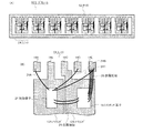
図6を参照して、この種の半導体装置100の構成を説明する。半導体装置100は、スイッチング素子103と、制御素子104と、スイッチング素子103が実装されるアイランド101と、制御素子104が実装されるアイランド102と、制御素子104またはスイッチング素子103と接続されて外部に導出するリード106と、これらを一体的に封止する封止樹脂107とを主要に備えている。 The configuration of this type of semiconductor device 100 will be described with reference to FIG. The semiconductor device 100 includes a switching element 103, a control element 104, an island 101 on which the switching element 103 is mounted, an island 102 on which the control element 104 is mounted, and the control element 104 or the switching element 103. Leads 106 to be led out and a sealing resin 107 for sealing them integrally are mainly provided.
スイッチング素子103は、例えばディスクリートのMOSFETであり、裏面のドレイン電極がアイランド101に接続され、表面のゲート電極が制御素子104と接続され、表面のソース電極が金属細線105を介してリード106Dに接続されている。一方、LSIから成る制御素子104は、表面に多数個の電極が設けられ、金属細線105を経由してスイッチング素子103やリード106A、106Bと接続される。
The switching element 103 is, for example, a discrete MOSFET, the drain electrode on the back surface is connected to the island 101, the gate electrode on the front surface is connected to the control element 104, and the source electrode on the front surface is connected to the
また、封止樹脂107の側面からは、リード106A〜106Eが導出しており、これらのリードを実装基板に挿入することにより、半導体装置100は差込実装される。
スイッチング素子103の裏面電極は数百Vの高電圧が印加される一方、制御素子104の裏面は周囲と絶縁される必要がある。従って、スイッチング素子103と制御素子104とを、導電性接着材を用いて同一のランドに固着すると、裏面に高電位が印加された制御素子104が誤動作してしまう恐れがある。 While a high voltage of several hundred volts is applied to the back electrode of the switching element 103, the back surface of the control element 104 needs to be insulated from the surroundings. Therefore, if the switching element 103 and the control element 104 are fixed to the same land using a conductive adhesive, the control element 104 having a high potential applied to the back surface may malfunction.
この誤作動を防止するために、半導体装置100では、スイッチング素子103が実装されるアイランド101と、制御素子104が実装されるアイランド102とを分離して形成している。この様にすることで、スイッチング素子103に印加される電圧が制御素子に与える悪影響が排除される。 In order to prevent this malfunction, in the semiconductor device 100, the island 101 on which the switching element 103 is mounted and the island 102 on which the control element 104 is mounted are formed separately. By doing so, the adverse effect of the voltage applied to the switching element 103 on the control element is eliminated.
また、上記した構成の半導体装置の製造方法は次の通りである。先ず、一枚の導電箔に対して、エッチング加工またはプレス加工を施すことにより、図6に示す形状のアイランド101、アイランド102およびリード106を形成する。次に、アイランド101の上面にスイッチング素子103を固着し、アイランド102の上面に制御素子104を固着する。更に、金属細線105を経由して、スイッチング素子103および制御素子104を所定のリードと接続する。次に、アイランド101、アイランド102およびリード106をモールド金型のキャビティに収納した後に、このキャビティに封止樹脂107を注入して樹脂封止の工程を行う。 The manufacturing method of the semiconductor device having the above-described configuration is as follows. First, an island 101, an island 102, and a lead 106 having the shape shown in FIG. 6 are formed by performing etching or pressing on one conductive foil. Next, the switching element 103 is fixed to the upper surface of the island 101, and the control element 104 is fixed to the upper surface of the island 102. Further, the switching element 103 and the control element 104 are connected to predetermined leads via the fine metal wire 105. Next, after the island 101, the island 102, and the lead 106 are accommodated in the cavity of the mold, a sealing resin 107 is injected into the cavity to perform a resin sealing process.
しかしながら、上記した半導体装置100では、樹脂封止の工程に於いて金属細線がリード106Bの先端部に接触してしまう問題があった。
However, in the semiconductor device 100 described above, there is a problem that the fine metal wire comes into contact with the tip of the
具体的には、上記した樹脂封止の工程では、図6に示す矢印の方向に、液状又は半固形状の状態の封止樹脂105を高圧でキャビティの中に注入する。このようにすると、各金属細線は、注入される封止樹脂による圧力を受ける。特に、金属細線105Aは、封止樹脂による圧力が大きく作用する。この理由は、金属細線105Aが、制御素子104と、端部に配置されたリード106Aとを接続するので、封止樹脂の流れる方向に対して傾斜する角度が大きくなるからである。従って、封止樹脂が注入される圧力により、金属細線106Aが点線で示す形状に湾曲して、隣接するリード106Bに接触してしまう恐れがある。金属細線106Aがリード106Bに接触したまま封止樹脂107が硬化してしまうと、使用状況下にて両者がショートしてしまうので不良が発生する。
Specifically, in the above-described resin sealing step, liquid or semi-solid sealing resin 105 is injected into the cavity at high pressure in the direction of the arrow shown in FIG. If it does in this way, each metal fine wire will receive the pressure by the sealing resin inject | poured. In particular, the metal
本発明は、上述した問題を鑑みて成されたものである。本発明の主な目的は、樹脂封止の工程の樹脂の注入圧による金属細線のショートが防止された半導体装置およびその製造方法を提供することにある。 The present invention has been made in view of the above-described problems. A main object of the present invention is to provide a semiconductor device in which a short circuit of a fine metal wire due to a resin injection pressure in a resin sealing step is prevented, and a method for manufacturing the same.
本発明の半導体装置は、互いに分離して形成された第1アイランドおよび第2アイランドと、前記第1アイランドの上面に固着された第1半導体素子と、前記第2アイランドの上面に固着された第2半導体素子と、前記第1アイランドおよび前記第2アイランドの一側辺の一端側に配置されたリードと、前記第1半導体素子の電極と、前記リードの前記一端側の上面とを接続する第1金属細線と、前記第2半導体素子の電極と、前記リードの他端側の上面とを接続する第2金属細線と、を備え、前記第1金属細線は前記第2金属細線の上方を延在すると共に、前記第1金属細線と前記第2金属細線とは平面視で交差することを特徴とする。 The semiconductor device according to the present invention includes a first island and a second island formed separately from each other, a first semiconductor element fixed to the upper surface of the first island, and a first island fixed to the upper surface of the second island. A second semiconductor element; a lead disposed on one end of one side of the first island and the second island; an electrode of the first semiconductor element; and an upper surface on the one end side of the lead. A thin metal wire, an electrode of the second semiconductor element, and a second thin metal wire that connects the upper surface of the other end of the lead. The first thin metal wire extends above the second thin metal wire. And the first metal fine wire and the second metal fine wire intersect each other in plan view.
本発明の半導体装置の製造方法は、第1アイランドと、前記第1アイランドと分離して形成された第2アイランドと、前記第1アイランドまたは前記第2アイランドに一端が接近する複数のリードを用意し、前記第1アイランドの上面に第1半導体素子を固着し、前記第2アイランドの上面に第2半導体素子を固着する工程と、前記第1アイランドおよび前記第2アイランドの一側辺の一端側に配置されたリードと前記第1半導体素子とを第1金属細線で接続し、前記第1金属細線と交差する第2金属細線により前記リードと前記第2半導体素子とを接続する工程と、モールド金型のキャビティに前記両アイランドおよび前記リードの一部を収納して、前記第1アイランドおよび第2アイランドの前記一側辺に対向する他側辺側から、前記キャビティに封止樹脂を注入する工程と、を備えたことを特徴とする。 According to a method of manufacturing a semiconductor device of the present invention, a first island, a second island formed separately from the first island, and a plurality of leads having one end approaching the first island or the second island are prepared. Fixing a first semiconductor element on the upper surface of the first island and fixing a second semiconductor element on the upper surface of the second island; and one end side of one side of the first island and the second island A lead connected to the first semiconductor element with a first metal fine wire, and connecting the lead and the second semiconductor element with a second metal thin wire intersecting the first metal fine wire; and a mold The both islands and a part of the lead are accommodated in a cavity of a mold, and the key from the other side opposite to the one side of the first island and the second island. Implanting sealing resin Activity, characterized by comprising a.
本発明によれば、樹脂封止時の圧力により他のリードに接触してしまう恐れがある第1金属細線を、第2金属細線と平面視で交差して配置させている。この様にすることで、樹脂封止の圧力により第1金属細線が湾曲したとしても、第2金属細線に第1金属細線が接触することにより、第1金属細線の過度の変形が抑制される。結果的に、第1金属細線が他のリードへ接触することによるショートが防止される。 According to the present invention, the first metal fine wire that may come into contact with other leads due to the pressure at the time of resin sealing is arranged so as to intersect the second metal fine wire in plan view. By doing in this way, even if a 1st metal fine wire curves by the pressure of resin sealing, an excessive deformation | transformation of a 1st metal fine wire is suppressed by a 1st metal fine wire contacting a 2nd metal fine wire. . As a result, a short circuit due to the first metal thin wire coming into contact with another lead is prevented.
図1を参照して、本実施の形態に係る半導体装置10の構成を説明する。 With reference to FIG. 1, the structure of the semiconductor device 10 according to the present embodiment will be described.
図1(A)を参照して、半導体装置10は、互いに分離されたアイランド12A(第1アイランド)およびアイランド12B(第2アイランド)と、アイランド12Aの上面に実装された制御素子20(第1半導体素子)と、アイランド12Bの上面に固着されたスイッチング素子18(第2半導体素子)と、外部接続端子として機能する複数のリード14と、これらを一体的に被覆して機械的に支持する封止樹脂16とを主要に備えた構成となっている。更に、制御素子20は複数の金属細線24A等を経由して各リード14と接続され、スイッチング素子18は複数の金属細線26を経由してリード14Eと接続される。
Referring to FIG. 1A, a semiconductor device 10 includes an island 12A (first island) and an island 12B (second island) separated from each other, and a control element 20 (first island) mounted on the upper surface of the island 12A. A semiconductor element), a switching element 18 (second semiconductor element) fixed to the upper surface of the island 12B, a plurality of leads 14 functioning as external connection terminals, and a cover that integrally covers and mechanically supports them. The structure mainly includes a stop resin 16. Further, the control element 20 is connected to each lead 14 via a plurality of
アイランド12Aおよびアイランド12Bは、厚みが0.4mm程度の銅を主材料とした板を、エッチング加工やパンチング加工により所定形状に成形したものである。アイランド12Aおよびアイランド12Bは、上面に実装される回路素子(制御素子20、スイッチング素子18)よりも平面視で若干大きく形成される。また、アイランド12Aから連続してリード14Bが外部に導出し、アイランド12Bから連続してリード14Cが外部に導出する。リード14Bおよびリード14Cは、製造工程において、アイランド12Aおよびアイランド12Bを機械的に支持する吊りリードとして機能する。
The island 12A and the island 12B are formed by etching a plate made mainly of copper having a thickness of about 0.4 mm into a predetermined shape by etching or punching. The island 12A and the island 12B are formed slightly larger in plan view than the circuit elements (the control element 20 and the switching element 18) mounted on the upper surface. Further, the
リード14は、内蔵されたスイッチング素子18または制御素子20と電気的に接続され、一部が外部に露出して外部接続端子として機能している。図1(A)を参照すると、リード14A−14Eが、アイランド12A、12Bの上辺(一側辺)に沿って配置されている。リード14A、14Dおよび14Eは、アイランド12A、12Bの面よりも上方に位置し(図1(C)参照)、金属細線を経由して制御素子20またはスイッチング素子18に接続される。一方、リード14Bはアイランド12Aと連続しており、中間部に段差加工が施されている。同様に、リード14Cもアイランド12Bと連続しており、中間部に段差加工が施されている。
The lead 14 is electrically connected to the built-in switching element 18 or control element 20, and a part of the lead 14 is exposed to the outside and functions as an external connection terminal. Referring to FIG. 1A, the
スイッチング素子18としては、MOSFET(Metal−Oxide Semiconductor Field Effect Transistor)、バイポーラトランジスタ、IGBT(Insulated Gate Bipolar Transistor)が採用される。スイッチング素子18としてMOSFETが採用された場合は、裏面にドレイン電極が形成され、バイポーラトランジスタが採用された場合は裏面にコレクタ電極が形成される。更に、本実施の形態では、一例として電源回路が半導体装置10に内蔵されるので、スイッチング素子18としては、例えば1A以上の大電流のスイッチングを行うパワー系の半導体素子(パワー素子)が採用される。 As the switching element 18, MOSFET (Metal-Oxide Semiconductor Field Effect Transistor), bipolar transistor, and IGBT (Insulated Gate Bipolar Transistor) are adopted. When a MOSFET is employed as the switching element 18, a drain electrode is formed on the back surface, and when a bipolar transistor is employed, a collector electrode is formed on the back surface. Furthermore, in the present embodiment, since the power supply circuit is built in the semiconductor device 10 as an example, a power semiconductor element (power element) that performs switching of a large current of, for example, 1 A or more is employed as the switching element 18. The
本実施の形態では、MOSFETがスイッチング素子18として採用され、下面のドレイン電極が導電性接着材を介してアイランド12Bの上面に接続され、上面のゲート電極は金属細線28を経由して制御素子20と接続され、上面のソース電極は複数の金属細線26を経由してリード14Eと接続される。そして、制御素子20から供給される制御信号に基づいて、スイッチング素子18はスイッチング動作を行う。
In the present embodiment, a MOSFET is employed as the switching element 18, the drain electrode on the lower surface is connected to the upper surface of the island 12 </ b> B via a conductive adhesive, and the gate electrode on the upper surface is connected to the control element 20 via the fine metal wire 28. The source electrode on the upper surface is connected to the
制御素子20は、スイッチング素子18のスイッチングを制御する回路が表面に形成されたLSIである。制御素子20は、素子裏面に貼着された絶縁シートおよび絶縁性接着材を介して、アイランド12Aに絶縁された状態で固着され、上面の電極は金属細線24を経由してリード14やスイッチング素子18と接続されている。具体的には、制御素子20は、リード14A、14Dと、金属細線24A、24Bを経由して接続されている。更に、制御素子20の電極と、スイッチング素子18の制御電極とは、金属細線28を経由して接続されている。制御素子20には、一定以上の温度を検知したときにスイッチング素子18を強制的にオフ状態とする過熱保護回路が内蔵されている。
The control element 20 is an LSI in which a circuit for controlling the switching of the switching element 18 is formed on the surface. The control element 20 is fixed in an insulated state to the island 12A via an insulating sheet and an insulating adhesive adhered to the back surface of the element, and the upper electrode is connected to the lead 14 and the switching element via the metal thin wire 24. 18 is connected. Specifically, the control element 20 is connected to the
更に、スイッチング素子18は、リード14が整列する方向(紙面上では横方向)に対して装置全体の右端付近に配置され、制御素子20は装置全体の中央部寄りに配置されている。 Further, the switching element 18 is disposed near the right end of the entire apparatus with respect to the direction in which the leads 14 are aligned (lateral direction on the paper surface), and the control element 20 is disposed near the center of the entire apparatus.
本実施の形態では、金属細線24、26、28としては、直径が40μm以下の金から成る金線が採用されている。高価な金の使用量を減らしてコストを低減させるために細い金線を用いているが、この様にすることで金属細線の機械的強度が低下して樹脂封止時に金属細線が変形する恐れがある。本実施の形態では、金属細線のレイアウトを最適化することにより、樹脂封止時に於ける金属細線の変形によるショートの発生を抑制している。この事項に関しては、図1(B)を参照して後述する。
In the present embodiment, gold wires made of gold having a diameter of 40 μm or less are adopted as the
封止樹脂16は、リード14の一部、アイランド12A、12B、スイッチング素子18、制御素子20、金属細線を一体的に被覆して全体を機械的に支持する機能を有する。封止樹脂16の材料としては、エポキシ樹脂等の熱硬化性樹脂や、アクリル樹脂等の熱可塑性樹脂が採用される。また、封止樹脂16には、放熱性向上およびSiチップと樹脂の熱膨張係数の違いにより発生する応力を抑制させるために、粒状のシリカやアルミナ等のフィラーが混入された樹脂材料から成る。 The sealing resin 16 has a function of mechanically supporting the whole of the lead 14 by integrally covering a part of the lead 14, the islands 12 </ b> A and 12 </ b> B, the switching element 18, the control element 20, and the fine metal wires. As the material of the sealing resin 16, a thermosetting resin such as an epoxy resin or a thermoplastic resin such as an acrylic resin is employed. Further, the sealing resin 16 is made of a resin material in which fillers such as granular silica and alumina are mixed in order to improve heat dissipation and suppress a stress generated due to a difference in thermal expansion coefficient between the Si chip and the resin.
図1(B)を参照して、金属細線24Cおよび金属細線26の構成を説明する。装置の右端に配置されたリード14Eは、電源電位に接続されており、制御素子20およびスイッチング素子18の両方に接続される。このため、リード14Eは、金属細線24Cを経由して制御素子20に接続され、複数の金属細線26を経由してスイッチング素子のソース電極と接続される。ここで、金属細線24Cの長さは例えば3mm以上である。
With reference to FIG. 1 (B), the structure of the metal
金属細線24Cは、一端が制御素子20の電極と接続され、他端がリード14Eに接続されている。更に、金属細線24Cの他端は、リード14Eの中央部よりも右側(外側)の領域に接続されている。この様にすることで、リード14Eに隣接されたリード14Dから、金属細線24Cを離間させることができる。具体的には、リード14Dと金属細線24Cとが離間する距離D1は、例えば0.5mm以上となる。リード14Eは接地電位と接続される一方、リード14Dは電位が異なる制御用の信号が通過する。従って、リード14Eに接続される金属細線24Cがリード14Dに接触するとショートが発生するが、このような構成にすることによりショートが防止される。
One end of the
金属細線26の一端はスイッチング素子18の上面に設けられた電極と接続され、他端はリード14Eの上面に接続される。ここで、一部の金属細線26の他端は、リード14Eの上面において、中心よりも左側(内側)に接続される。
One end of the
更に、金属細線24Cは、金属細線26の上方を交差するように配置されており、このことにより金属細線24Cの変形が抑制される。具体的には、図1(B)に示すように、金属細線24Cは、中央部に配置される制御素子20と、端部のリード14Eと接続している。従って、製造工程の樹脂封止の段階にて供給される封止樹脂の流れにより、金属細線24Cには他の金属細線よりも大きな圧力が作用する。このことから、金属細線24Cは変形しやすい条件下にあり、上記したショートを防止するためにも変形を抑制する必要がある。更に、図1(C)を参照して、金属細線が接続されるリード14E(ポスト)は、スイッチング素子18や制御素子20よりも上方に位置している。従って、両者を接続する金属細線24Cが、樹脂の注入圧力により紙面上にて右方向に変形すると、図1(B)に示すリード14Dの下端に金属細線24Cが容易に接触してしまう。
Further, the
上記したショートを防止するために、本実施形態では、金属細線26の上方を交差するように金属細線24Cを配置している。この様にすることで、樹脂の封入圧により金属細線24Cがリード14D側に変形しても、金属細線26により金属細線24Cが支持される。結果的に、金属細線24Cの変形が抑制され、金属細線24Cがリード14Dに接触することが防止される。これは、金属細線24Cも金属細線26も同じリード14Eに接続されるため、仮に接触しても同電位で、故障しないから実現可能である。
In order to prevent the short circuit described above, in the present embodiment, the
更に、本実施形態では、金属細線24Cが、複数の金属細線26により支持されているので、複数の金属細線26によりサポートされる支持力が大きく、金属細線24Cの変形を防止する効果が非常に大きくなっている。更に、リード14Eに接続される金属細線26の一部は、リード14Eの上面において中央よりも左側(中央側)に接続されている。この様にすることで、金属細線24Cと金属細線26とを確実に平面視で交差させることができる。
Furthermore, in this embodiment, since the
図2から図5を参照して、上記した構成の半導体装置の製造方法を説明する。 With reference to FIGS. 2 to 5, a method of manufacturing the semiconductor device having the above-described configuration will be described.
先ず、図2を参照して、所定形状のリードフレーム50を用意する。図2(A)はリードフレーム50全体を示す平面図であり、図2(B)はリードフレーム50に含まれるユニット54を示す斜視図である。
First, referring to FIG. 2, a
図2(A)を参照して、リードフレーム50の外形は短冊形状であり、枠状の外枠52の内部に複数個のユニット54が形成されている。ここでユニットとは、1つの半導体装置を構成する部位の集まりである。図では、額縁状の外枠52と連結された7個のユニット54が示されているが、外枠52の内部にマトリックス状に多数個のユニット54が設けられても良い。ここで、以下の各工程は、リードフレーム50の各ユニット54に対して一括して行われる。
Referring to FIG. 2A, the outer shape of the
図2(B)を参照して、1つのユニット54は、2つのアイランド12A、12Bと、アイランド12A、12Bに一端が接近する複数のリード14A−14Eとから成る。アイランド12A、12Bは、上面に半導体素子が載置可能な大きさである。アイランド12Aからはリード14Bが一体的に延在して外枠52と連結されている。また、アイランド12Bからはリード14Cが一体的に延在して外枠52と連結されている。即ち、リード14Bおよびリード14Cは、アイランド12Aおよびアイランド12Bを外枠52に固定する為の吊りリードとしても機能している。リード14A、14D、14Eは、一端がアイランド12A、12Bに接近して他端は外枠52に連結されている。
Referring to FIG. 2B, one
更に、各ユニット54のアイランド12Aおよびアイランド12Bの上面には所定の回路素子が実装される。具体的には、アイランド12Aの上面には制御素子20が実装され、アイランド12Bの上面にはスイッチング素子18が実装される。制御素子20は、裏面に樹脂シートが貼着された状態で、エポキシ樹脂等の絶縁性接着材を介してアイランド12Aの上面に実装される。一方、スイッチング素子18は、導電性ペーストや半田等の導電性固着材を介して、アイランド12Bの上面に実装される。またここで、制御素子20とスイッチング素子18とは、分離されたアイランドに各々が実装されているので、導電性の固着材を用いて制御素子20をアイランド12Aに実装しても、両者はショートを起こさない。
Further, predetermined circuit elements are mounted on the top surfaces of the islands 12A and 12B of each
図3を参照して、次に、アイランド12A、12Bに固着された各素子の電気的接続を行う。図3(A)は本工程を示す平面図であり、図3(B)は1つのユニット54を拡大した平面図である。
Referring to FIG. 3, next, each element fixed to islands 12A and 12B is electrically connected. FIG. 3A is a plan view showing this step, and FIG. 3B is an enlarged plan view of one
図3(B)を参照して、本工程では、直径が40μm程度の金から成る金属細線を用いて、制御素子20およびスイッチング素子18の電気的接続を行う。制御素子20の上面に設けられた電極は、リード14A、14D、14Eと、金属細線24A、24B、24Cを経由して接続される。また、スイッチング素子18の上面に設けられたソース電極は、複数の金属細線26を介して、リード14Eと接続される。更に、スイッチング素子18のゲート電極は、金属細線28を介して制御素子20の電極と接続される。
Referring to FIG. 3B, in this step, the control element 20 and the switching element 18 are electrically connected using a fine metal wire made of gold having a diameter of about 40 μm. The electrodes provided on the upper surface of the control element 20 are connected to the
制御素子20とリード14Eとを接続する金属細線24Cは、金属細線26の上方を交差して配置されている。本工程では、先ず、スイッチング素子18のソース電極とリード14Eとを金属細線26を経由して接続する。金属細線26の一端は、スイッチング素子18のソース電極に等間隔にボールボンディングされる。そして、金属細線26の他端は、リード14Eの端部付近に等間隔にスティッチボンディングされる。スイッチング素子18のソース電極は大電流が通過するので、オン抵抗を低減するために複数の金属細線26が用いられる。
The
金属細線26の接続が終了した後に、制御素子20とリード14Eとを金属細線24Cにより接続する。金属細線24Cの一端は、制御素子20の一番右側にある電極と接続され、他端はリード14Eと接続される。このとき、金属細線24Cの他端は、リード14Eの中央よりも右側(外側)に配置される。この様にすることで、リード14Eに隣り合うリード14Dと、金属細線24Cとを離間させて、両者のショートを防止できる。
After the connection of the
図4を参照して、次に、制御素子20等が被覆されるように樹脂封止を行う。図4(A)は本工程を示す断面図であり、図4(B)は本工程を示す平面図であり、図4(C)は拡大された断面図である。 Referring to FIG. 4, next, resin sealing is performed so as to cover control element 20 and the like. 4A is a cross-sectional view showing this step, FIG. 4B is a plan view showing this step, and FIG. 4C is an enlarged cross-sectional view.
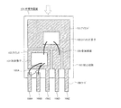
図4(A)を参照して、本工程では、モールド金型56を用いて樹脂封止を行う。このモールド金型56は、上金型58と下金型60とから成り、両者を当接させることで、封止樹脂が注入されるキャビティ62が形成される。樹脂封止の方法としては、熱硬化性樹脂を用いるトランスファーモールドが採用される。 Referring to FIG. 4A, in this step, resin sealing is performed using a mold die 56. The mold 56 is composed of an upper mold 58 and a lower mold 60, and a cavity 62 into which a sealing resin is injected is formed by bringing them into contact with each other. As a resin sealing method, a transfer mold using a thermosetting resin is employed.
具体的な封止方法は、先ず、前工程のワイヤボンディングが終了したアイランド12Aおよびアイランド12Bを、キャビティ62に収納する。このとき、封止圧によりアイランド12Aが浮上することを防止するために、アイランド12Aの先端部付近は、押圧部(可動ピン)64、66により押圧されて厚み方向に固定されている。同様に、アイランド12Bの上下主面も押圧部により固定される。押圧部64は、上金型58に備えられた可動式のピンであり、下端がアイランド12Aの上面に接触している。押圧部66は、下金型60に設けられた可動式のピンであり、上端がアイランド12Aの下面に接触している。次に、モールド金型56に設けたゲート46からキャビティ62の内部に封止樹脂を注入して、アイランド12A、12B、制御素子20、スイッチング素子18、リード14および各金属細線を樹脂封止する。封止樹脂の注入に伴い、キャビティ62の内部の空気はエアベント48を経由して外部に放出される。 As a specific sealing method, first, the island 12A and the island 12B that have undergone the wire bonding in the previous step are accommodated in the cavity 62. At this time, in order to prevent the island 12A from rising due to the sealing pressure, the vicinity of the tip of the island 12A is pressed by the pressing portions (movable pins) 64 and 66 and fixed in the thickness direction. Similarly, the upper and lower main surfaces of the island 12B are also fixed by the pressing portion. The pressing portion 64 is a movable pin provided in the upper mold 58, and the lower end is in contact with the upper surface of the island 12A. The pressing part 66 is a movable pin provided in the lower mold 60, and its upper end is in contact with the lower surface of the island 12A. Next, a sealing resin is injected from the gate 46 provided in the mold 56 into the cavity 62, and the islands 12A and 12B, the control element 20, the switching element 18, the lead 14, and the respective metal wires are sealed with the resin. . As the sealing resin is injected, the air inside the cavity 62 is discharged to the outside via the air vent 48.
更に本工程では、キャビティ62に注入された封止樹脂が硬化する途中段階で押圧部64、66を引き抜いているので、アイランド12Aの上面および下面は封止樹脂により覆われ外部には露出しない。 Further, in this step, the pressing portions 64 and 66 are pulled out while the sealing resin injected into the cavity 62 is cured, so that the upper and lower surfaces of the island 12A are covered with the sealing resin and are not exposed to the outside.
同様に、アイランド12Bの上面および下面も、上記した押圧部により固定される。 Similarly, the upper surface and the lower surface of the island 12B are also fixed by the pressing portion described above.
図4(B)を参照して、ゲート46から液状または半固形状の封止樹脂がキャビティ62に注入されると、注入された封止樹脂による圧力で、金属細線は湾曲する。特に、端部に配置されたリード14Eと制御素子20とを接続する金属細線24Cは、封止樹脂の流れに対して傾斜して配置されるので、樹脂による圧力が大きくなり変形する恐れがある。
Referring to FIG. 4B, when a liquid or semi-solid sealing resin is injected from the gate 46 into the cavity 62, the fine metal wire is bent by the pressure of the injected sealing resin. In particular, since the metal
図4(C)に変形した状態の金属細線24Cを示す。ここでは、変形する前の金属細線24Cを点線にて示し、変形した後の状態の金属細線24Cを実線にて示している。上記したように、金属細線24Cは、金属細線26の上方にて交差するように配置されている。従って、樹脂圧により金属細線24Cがリード14D側に変形すると、金属細線26に接触して支持され、この時点で金属細線24Cの変形がストップする。このことにより、変形した金属細線24Cがリード14Dに接触することが防止される。更に本工程では、金属細線24Cの下方に、複数の金属細線26が設けられている。従って、樹脂封止時に於いて、複数の金属細線26による充分な支持力により、金属細線24Cの変形が抑制される。また、金属細線26は、封止樹脂の流れに対して、金属細線24Cよりも平行に形成されているので、封止樹脂の圧力による変形は比較的に小さい。
FIG. 4C shows a deformed metal
図5に樹脂封止が終了した後のリードフレーム50を示す。ここでは、リードフレーム50に設けられた各ユニット54が一括して同時に樹脂封止される。
FIG. 5 shows the
本工程が終了した後は、打ち抜き加工を行うことで、リードフレーム50の外枠52から各ユニット54のリードを分離し、分離された半導体装置を、例えば実装基板上に実装する。また、外部に露出するリードの酸化を防止するために、リードの表面を半田メッキ等のメッキ膜により被覆する。
After this process is completed, the lead of each
以上の工程により、図1に構造を示す半導体装置10が製造される。 Through the above steps, the semiconductor device 10 whose structure is shown in FIG. 1 is manufactured.
10 半導体装置
12A、12B アイランド
14、14A、14B、14C、14D、14E リード
16 封止樹脂
18 スイッチング素子
20 制御素子
24、24A、24B、24C 金属細線
26、26A、26B、26C 金属細線
28 金属細線
46 ゲート
48 エアベント
50 リードフレーム
52 外枠
54 ユニット
56 モールド金型
58 上金型
60 下金型
62 キャビティ
64 押圧部
66 押圧部
10 Semiconductor device 12A,
Claims (8)
前記第1アイランドの上面に固着された第1半導体素子と、
前記第2アイランドの上面に固着された第2半導体素子と、
前記第1アイランドおよび前記第2アイランドの一側辺の一端側に配置されたリードと、
前記第1半導体素子の電極と、前記リードの前記一端側の上面とを接続する第1金属細線と、
前記第2半導体素子の電極と、前記リードの他端側の上面とを接続する第2金属細線と、を備え、
前記第1金属細線は前記第2金属細線の上方を延在すると共に、前記第1金属細線と前記第2金属細線とは平面視で交差することを特徴とする半導体装置。 A first island and a second island formed separately from each other;
A first semiconductor element fixed to the upper surface of the first island;
A second semiconductor element fixed to the upper surface of the second island;
A lead disposed on one end of one side of the first island and the second island;
A first fine metal wire connecting the electrode of the first semiconductor element and the upper surface of the one end side of the lead;
A second thin metal wire connecting the electrode of the second semiconductor element and the upper surface of the other end of the lead;
The first metal fine wire extends above the second metal fine wire, and the first metal fine wire and the second metal fine wire intersect each other in plan view.
前記第1アイランドおよび前記第2アイランドの一側辺の一端側に配置されたリードと前記第1半導体素子とを第1金属細線で接続し、前記第1金属細線と交差する第2金属細線により前記リードと前記第2半導体素子とを接続する工程と、
モールド金型のキャビティに前記両アイランドおよび前記リードの一部を収納して、前記第1アイランドおよび第2アイランドの前記一側辺に対向する他側辺側から、前記キャビティに封止樹脂を注入する工程と、
を備えたことを特徴とする半導体装置の製造方法。 Preparing a first island, a second island formed separately from the first island, and a plurality of leads having one end approaching the first island or the second island; Fixing one semiconductor element and fixing the second semiconductor element on the upper surface of the second island;
A lead disposed on one end of one side of the first island and the second island and the first semiconductor element are connected by a first metal thin wire, and a second metal thin wire intersecting the first metal thin wire is used. Connecting the lead and the second semiconductor element;
The both islands and a part of the lead are accommodated in the cavity of the mold, and sealing resin is injected into the cavity from the other side opposite to the one side of the first island and the second island. And the process of
A method for manufacturing a semiconductor device, comprising:
前記封止樹脂の注入圧により変形した前記第1金属細線が前記第2金属細線に接触することを特徴とする請求項6記載の半導体装置の製造方法。 In the step of injecting the sealing resin,
7. The method of manufacturing a semiconductor device according to claim 6, wherein the first metal thin wire deformed by the injection pressure of the sealing resin contacts the second metal thin wire.
前記封止樹脂を注入する工程では、前記複数の第2金属細線に前記第1金属細線が接触することを特徴とする請求項7記載の半導体装置の製造方法。 In the connecting step, the second semiconductor element and the lead are connected by a plurality of the second thin metal wires,
8. The method of manufacturing a semiconductor device according to claim 7, wherein in the step of injecting the sealing resin, the first metal fine wires are in contact with the plurality of second metal fine wires.
Priority Applications (4)
| Application Number | Priority Date | Filing Date | Title |
|---|---|---|---|
| JP2009045570A JP2010199492A (en) | 2009-02-27 | 2009-02-27 | Semiconductor device and method of manufacturing same |
| PCT/JP2010/053489 WO2010098501A1 (en) | 2009-02-27 | 2010-02-25 | Semiconductor device and method of producing same |
| CN201080009373.5A CN102334186B (en) | 2009-02-27 | 2010-02-25 | Semiconductor device and method of producing same |
| US13/203,447 US8633511B2 (en) | 2009-02-27 | 2010-02-25 | Method of producing semiconductor device packaging having chips attached to islands separately and covered by encapsulation material |
Applications Claiming Priority (1)
| Application Number | Priority Date | Filing Date | Title |
|---|---|---|---|
| JP2009045570A JP2010199492A (en) | 2009-02-27 | 2009-02-27 | Semiconductor device and method of manufacturing same |
Publications (2)
| Publication Number | Publication Date |
|---|---|
| JP2010199492A true JP2010199492A (en) | 2010-09-09 |
| JP2010199492A5 JP2010199492A5 (en) | 2011-10-20 |
Family
ID=42665695
Family Applications (1)
| Application Number | Title | Priority Date | Filing Date |
|---|---|---|---|
| JP2009045570A Pending JP2010199492A (en) | 2009-02-27 | 2009-02-27 | Semiconductor device and method of manufacturing same |
Country Status (4)
| Country | Link |
|---|---|
| US (1) | US8633511B2 (en) |
| JP (1) | JP2010199492A (en) |
| CN (1) | CN102334186B (en) |
| WO (1) | WO2010098501A1 (en) |
Cited By (1)
| Publication number | Priority date | Publication date | Assignee | Title |
|---|---|---|---|---|
| JP2019054296A (en) * | 2019-01-10 | 2019-04-04 | 京セラ株式会社 | Power semiconductor module |
Families Citing this family (6)
| Publication number | Priority date | Publication date | Assignee | Title |
|---|---|---|---|---|
| JP6161251B2 (en) * | 2012-10-17 | 2017-07-12 | ルネサスエレクトロニクス株式会社 | Semiconductor device and manufacturing method thereof |
| WO2014064822A1 (en) * | 2012-10-26 | 2014-05-01 | 株式会社日立産機システム | Power semiconductor module, and power conversion device provided with same |
| US10290907B2 (en) | 2015-07-27 | 2019-05-14 | Semiconductor Components Industries, Llc | Automatically programmable battery protection system and related methods |
| US10186498B2 (en) | 2015-07-27 | 2019-01-22 | Semiconductor Components Industries, Llc | Semiconductor leadframes and packages with solder dams and related methods |
| US10205330B2 (en) | 2015-07-27 | 2019-02-12 | Semiconductor Components Industries, Llc | Programmable battery protection system and related methods |
| CN107408553B (en) * | 2016-03-11 | 2019-07-26 | 新电元工业株式会社 | Semiconductor device |
Family Cites Families (11)
| Publication number | Priority date | Publication date | Assignee | Title |
|---|---|---|---|---|
| JPH01183129A (en) * | 1988-01-18 | 1989-07-20 | Fujitsu Ltd | Semiconductor device |
| JPH0350758A (en) * | 1989-07-18 | 1991-03-05 | Toshiba Corp | Resin seal type semiconductor device |
| US5309322A (en) * | 1992-10-13 | 1994-05-03 | Motorola, Inc. | Leadframe strip for semiconductor packages and method |
| JPH06177312A (en) * | 1992-12-08 | 1994-06-24 | Fuji Electric Co Ltd | Semiconductor device and lead frame |
| US5625235A (en) * | 1995-06-15 | 1997-04-29 | National Semiconductor Corporation | Multichip integrated circuit module with crossed bonding wires |
| US5739582A (en) * | 1995-11-24 | 1998-04-14 | Xerox Corporation | Method of packaging a high voltage device array in a multi-chip module |
| JP3308461B2 (en) * | 1996-11-14 | 2002-07-29 | 富士通株式会社 | Semiconductor device and lead frame |
| JP3474736B2 (en) * | 1997-08-29 | 2003-12-08 | トリニティ工業株式会社 | Temperature / humidity controller and temperature / humidity control method for air conditioner |
| KR100335481B1 (en) * | 1999-09-13 | 2002-05-04 | 김덕중 | Power device having multi-chip package structure |
| JP2001320009A (en) | 2000-05-10 | 2001-11-16 | Matsushita Electric Ind Co Ltd | Semiconductor device |
| TWI236126B (en) * | 2002-07-02 | 2005-07-11 | Alpha & Omega Semiconductor | Integrated circuit package for semiconductor devices with improved electric resistance and inductance |
-
2009
- 2009-02-27 JP JP2009045570A patent/JP2010199492A/en active Pending
-
2010
- 2010-02-25 CN CN201080009373.5A patent/CN102334186B/en not_active Expired - Fee Related
- 2010-02-25 WO PCT/JP2010/053489 patent/WO2010098501A1/en active Application Filing
- 2010-02-25 US US13/203,447 patent/US8633511B2/en active Active
Cited By (1)
| Publication number | Priority date | Publication date | Assignee | Title |
|---|---|---|---|---|
| JP2019054296A (en) * | 2019-01-10 | 2019-04-04 | 京セラ株式会社 | Power semiconductor module |
Also Published As
| Publication number | Publication date |
|---|---|
| US8633511B2 (en) | 2014-01-21 |
| WO2010098501A1 (en) | 2010-09-02 |
| CN102334186A (en) | 2012-01-25 |
| CN102334186B (en) | 2014-05-14 |
| US20110309408A1 (en) | 2011-12-22 |
Similar Documents
| Publication | Publication Date | Title |
|---|---|---|
| US8203848B2 (en) | Circuit device and method of manufacturing the same | |
| JP4614586B2 (en) | Method for manufacturing hybrid integrated circuit device | |
| WO2010098501A1 (en) | Semiconductor device and method of producing same | |
| US8105883B2 (en) | Molding die with tilted runner, method of manufacturing semiconductor device using the same, and semiconductor device made by the method | |
| JP2009534869A (en) | Semiconductor die package including multiple die and common node structure | |
| JP2002208656A (en) | Semiconductor device | |
| JPWO2016072012A1 (en) | Power semiconductor device and manufacturing method thereof | |
| JP2012015202A (en) | Semiconductor device, and method of manufacturing the same | |
| JP2010034350A (en) | Semiconductor device | |
| US9331041B2 (en) | Semiconductor device and semiconductor device manufacturing method | |
| JP2010034349A (en) | Method of manufacturing semiconductor device and lead frame | |
| JP2009071154A (en) | Semiconductor apparatus | |
| JP5161688B2 (en) | Semiconductor device and semiconductor module | |
| JP5341339B2 (en) | Circuit equipment | |
| JP2011204863A (en) | Semiconductor device, and method of manufacturing the same | |
| JP2009206406A (en) | Power semiconductor device | |
| JP4732138B2 (en) | Semiconductor device and manufacturing method thereof | |
| JP2008166621A (en) | Semiconductor device and manufacturing method thereof | |
| JP5341473B2 (en) | Semiconductor device and manufacturing method thereof | |
| JP5972158B2 (en) | Semiconductor device and manufacturing method of semiconductor device | |
| JP2004349300A (en) | Semiconductor device and its manufacturing method | |
| JP5132407B2 (en) | Semiconductor device | |
| JP2005051109A (en) | Power semiconductor module | |
| JP2013187268A (en) | Semiconductor module | |
| JP4676252B2 (en) | Circuit device manufacturing method |
Legal Events
| Date | Code | Title | Description |
|---|---|---|---|
| A711 | Notification of change in applicant |
Free format text: JAPANESE INTERMEDIATE CODE: A711 Effective date: 20110606 |
|
| A521 | Request for written amendment filed |
Free format text: JAPANESE INTERMEDIATE CODE: A523 Effective date: 20110901 |
|
| A621 | Written request for application examination |
Free format text: JAPANESE INTERMEDIATE CODE: A621 Effective date: 20120123 |
|
| A711 | Notification of change in applicant |
Free format text: JAPANESE INTERMEDIATE CODE: A711 Effective date: 20130218 |
|
| A521 | Request for written amendment filed |
Free format text: JAPANESE INTERMEDIATE CODE: A523 Effective date: 20130408 |
|
| A131 | Notification of reasons for refusal |
Free format text: JAPANESE INTERMEDIATE CODE: A131 Effective date: 20130625 |
|
| A02 | Decision of refusal |
Free format text: JAPANESE INTERMEDIATE CODE: A02 Effective date: 20131119 |