JP2010146418A - Touch panel corresponding to narrow frame lcd - Google Patents
Touch panel corresponding to narrow frame lcd Download PDFInfo
- Publication number
- JP2010146418A JP2010146418A JP2008324831A JP2008324831A JP2010146418A JP 2010146418 A JP2010146418 A JP 2010146418A JP 2008324831 A JP2008324831 A JP 2008324831A JP 2008324831 A JP2008324831 A JP 2008324831A JP 2010146418 A JP2010146418 A JP 2010146418A
- Authority
- JP
- Japan
- Prior art keywords
- electrode
- touch panel
- lcd
- narrow frame
- electrodes
- Prior art date
- Legal status (The legal status is an assumption and is not a legal conclusion. Google has not performed a legal analysis and makes no representation as to the accuracy of the status listed.)
- Granted
Links
Images

Landscapes
- Liquid Crystal (AREA)
- Position Input By Displaying (AREA)
Abstract
Description
本発明はLCD(液晶ディスプレイ・Liquid Crystal Display)の表面に貼って用いるタッチパネルに関し、特にLCDの縁に形成する枠部分、即ち額縁部分が小さい狭額縁LCDに対応可能な構造とした、狭額縁LCD対応タッチパネルに関する。 The present invention relates to a touch panel used by being attached to the surface of an LCD (Liquid Crystal Display), and in particular, a narrow frame LCD having a structure that can accommodate a narrow frame LCD having a small frame portion, that is, a frame portion formed on the edge of the LCD. It relates to a compatible touch panel.
近年広く普及しているLCDの技術進歩により、LCDの周囲に形成するフレームである額縁部分をできる限り狭くし、LCD装置全体に対してできる限り広い画面表示を行うことができるようにした、狭額縁LCDが用いられるようになっている。即ち、同じ外形寸法のLCD表示装置でも、実際のLCD表示画面の縁に形成する枠は小さいほど大きなLCD表示画面を形成できるため、LCDの縁に形成している引き出し線等を配置する部分を狭く形成した狭額縁LCDとすることが行われている。 Due to the technological advancement of LCDs that have become widespread in recent years, the frame portion that is a frame formed around the LCD is made as narrow as possible, and the entire LCD device can be displayed as wide as possible. A frame LCD is used. That is, even with an LCD display device having the same outer dimensions, a smaller LCD frame can be formed with a smaller frame formed on the edge of the actual LCD display screen. Narrow frame LCDs are being made narrow.
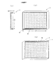
例えばアモルファスシリコンLCD(a−Si LCD)の外形は図10に示すように、狭額縁の辺と広額縁の辺とが存在する。即ち、縦と横の片側の辺にはそれぞれ各辺だけの引き出し線部分のみが存在する狭額縁となっているのに対して、他の片側の辺については、縦の他の辺部分にはゲートドライバIC(Gate Driver IC:GDIC)を配置し、横の他の辺部分にはソースドライバIC(Sourse Driver IC:SDIC)が配置するためにそれぞれ広額縁となっている。なお、GDIC及びSDICはそれぞれ関連する制御回路を配置したFPC(Flexible Printed Circuits)、即ちフレキシブルプリント基板に接続している。更に低温ポリシリコンLCDの場合は、ガラス上にこのドライバICを作り込めるため、全辺を狭額縁とした画面とすることができる。 For example, as shown in FIG. 10, the outer shape of an amorphous silicon LCD (a-Si LCD) has a narrow frame side and a wide frame side. In other words, each of the vertical and horizontal sides has a narrow frame with only a lead line portion for each side, whereas for the other side, the other side portion has a vertical frame. A gate driver IC (GDIC) is arranged, and a source driver IC (SDIC) is arranged on the other side part of the side, so that each frame has a wide frame. The GDIC and SDIC are connected to FPC (Flexible Printed Circuits), that is, flexible printed circuit boards, each of which has a related control circuit. Furthermore, in the case of a low-temperature polysilicon LCD, since this driver IC can be made on glass, a screen with a narrow frame on all sides can be obtained.
一方、従来より各種画面に透明なタッチパネルを貼り、画面に表示されている例えば各種指示入力画像部に指等を接触させることによって、タッチパネルに形成されている各種手法による接触位置検出手段により、画面全体のX−Y位置を検出し、利用者の指示がその位置に表示されている画面の指示である、として所定の入力を行っている。このような利用者による指示は単なる指示した点ではなく、それをなぞったことにより線、更には面を指示し、或いはこれを表示することが可能である。 On the other hand, a transparent touch panel is conventionally pasted on various screens, and the screen is detected by contact position detection means using various methods formed on the touch panel by, for example, bringing a finger or the like into contact with various instruction input image portions displayed on the screen. The entire XY position is detected, and a predetermined input is made assuming that the user's instruction is an instruction of a screen displayed at the position. Such an instruction by the user is not a point that is simply instructed, but by tracing it, it is possible to instruct a line or even a surface or display it.
このようなタッチパネルには各種の手法が存在するが、位置検出精度が良く、安定して作動し、故障が少なく、比較的安価に製造できることから抵抗膜方式が広く用いられている。この抵抗膜方式にも種々の方式が存在するが、多くのものはベースとなるガラス基板の表面に厚さ5〜10μm程度の、上下のパネルを貼り合わせるためのシール材、並びに上下の電極間の短絡を防ぐドットスペーサを適宜配置し、その表面に弾力性のある200μm程度のガラスかPETのシートを貼り付けたものが用いられている。このガラス基板とシートとが向かい合っている面には、それぞれITO(Indium Tin Oxide)と呼ばれる透明な電極が設けられている。抵抗膜方式の電極構成としては、例えば図7(a)に示すような縦横ともに対向する辺の縁部分にX電極とY電極とを1個ずつ配置する4線式、或いは同図(b)に示すように、X電極とY電極を2個ずつ設けた8線式等が用いられており、4線式より8線式の方が高性能であるものの、この縁部分を広く形成する必要がある。 There are various methods for such a touch panel, but the resistive film method is widely used because it has high position detection accuracy, operates stably, has few failures, and can be manufactured at a relatively low cost. There are various types of resistive film methods, but many of them are a seal material for bonding upper and lower panels having a thickness of about 5 to 10 μm on the surface of a glass substrate serving as a base, and between upper and lower electrodes. A dot spacer for preventing the short circuit is appropriately disposed, and an elastic glass or PET sheet of about 200 μm is attached to the surface thereof. Transparent electrodes called ITO (Indium Tin Oxide) are provided on the surfaces where the glass substrate and the sheet face each other. As the electrode configuration of the resistive film type, for example, as shown in FIG. 7A, a four-wire type in which one X electrode and one Y electrode are arranged at the edge portions of the sides facing both vertically and horizontally, or FIG. As shown in the figure, an 8-wire type with two X electrodes and two Y electrodes is used. Although the 8-wire type has higher performance than the 4-wire type, it is necessary to form a wide edge portion. There is.
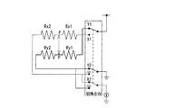
これらの電極構成において、最も基本的な構成である4線式について、指等による指示点の検出を行うタッチ位置検出手法を図7(c)に示している。同図に示す例においては、固定電極はX−Y軸についてY方向の位置を検出するために合い対向する横の辺にY1電極とY2電極とを設け、この電極に対してY1電極側を+、Y2電極側を−となる電圧をかけている。同図上にこの固定電極と図示していないスペーサを挟んで対向している可動電極についてはX方向の位置を検出するために、縦の辺にX1電極とX2電極とを設け、この電極に対してX1電極側を+、X2電極側を−となる電圧をかける。 FIG. 7C shows a touch position detection method for detecting a point indicated by a finger or the like for the four-wire type which is the most basic configuration in these electrode configurations. In the example shown in the figure, the fixed electrode is provided with a Y1 electrode and a Y2 electrode on opposite sides to detect the position in the Y direction with respect to the XY axis, and the Y1 electrode side is provided with respect to this electrode. A voltage of − is applied to the + and Y2 electrode sides. In order to detect the position in the X direction of the movable electrode facing this fixed electrode with a spacer (not shown) on the same figure, an X1 electrode and an X2 electrode are provided on the vertical side, In contrast, a voltage of + on the X1 electrode side and − on the X2 electrode side is applied.
このような電極構成により、利用者がこのタッチパネルの任意の位置であるP点を押す時、可動電極側の抵抗膜がスペーサの方向に撓んで固定電極側の抵抗膜に接触することにより、可動電極側と固定電極側の抵抗膜において分圧抵抗が生じ、これを求めることができる。即ち図示の例では可動電極側においてP点を挟んでX1電極側はRx1、X2電極側はRx2となる。同様に固定電極側はP点を挟んでY1電極側はRy1、Y2電極側はy2となる。 With such an electrode configuration, when the user presses the point P, which is an arbitrary position on the touch panel, the movable electrode side resistive film bends in the direction of the spacer and comes into contact with the fixed electrode side resistive film. A voltage dividing resistance is generated in the resistance film on the electrode side and the fixed electrode side, and this can be obtained. That is, in the illustrated example, the X1 electrode side is Rx1 and the X2 electrode side is Rx2 across the point P on the movable electrode side. Similarly, the Y1 electrode side is Ry1 and the Y2 electrode side is y2 across the point P on the fixed electrode side.
その結果図9に示すように、前記指示点PでX側とY側が接触する際、前記各抵抗Rx1とRx2及びRy1とRy2が生じると、抵抗値測定用切換SWによって切り替えた時の電圧を電圧計Vによってそれぞれ測定することにより、X方向のP点の位置及びY方向のP点の位置を検出することができる。なお、図示の例にではP点のX方向の位置をExとして検出し、スイッチSWを切り替えることによりEyとしてY方向の位置を検出する。 As a result, as shown in FIG. 9, when the resistances Rx1 and Rx2 and Ry1 and Ry2 occur when the X side and the Y side contact at the indicated point P, the voltage when switched by the resistance value measurement switch SW is changed. By measuring each with the voltmeter V, the position of the P point in the X direction and the position of the P point in the Y direction can be detected. In the illustrated example, the position of the point P in the X direction is detected as Ex, and the position in the Y direction is detected as Ey by switching the switch SW.
上記のようにタッチパネルにおいては、抵抗を検出するためのタッチ検出面のほか、電極、及びその電極への電源系統、並びに抵抗値を測定するための信号の回路を形成したFPCへ接続する取り出し部へのリード回路、等が必須のものとなる。したがってタッチ検出面の周囲に形成した電極の外側に、スペースを介してリード回路等を配置する必要があり、電極部分が存在する辺ではこれらの配置のために4〜8mmの幅が必要となっていた。特にリード回路は、抵抗値の増大や切断のし易さのために、所定以上は細くすることができず、この部分を狭くするには限界がある。なお、上記のような電極部分及びリード回路は、タッチパネルを備えたLCDの完成品となった時には、製品のカバー部分やモールド部分として保護している。 As described above, in the touch panel, in addition to the touch detection surface for detecting resistance, an extraction unit connected to an FPC in which an electrode, a power supply system to the electrode, and a signal circuit for measuring a resistance value are formed A lead circuit, etc. are essential. Therefore, it is necessary to arrange a lead circuit or the like outside the electrode formed around the touch detection surface via a space, and a width of 4 to 8 mm is necessary for the arrangement on the side where the electrode portion exists. It was. In particular, the lead circuit cannot be made thinner than a predetermined value because of an increase in resistance value or ease of cutting, and there is a limit to narrowing this portion. Note that the electrode part and the lead circuit as described above are protected as a cover part or a mold part of the product when an LCD having a touch panel is completed.
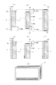
図8(a)〜(f)には抵抗膜方式タッチパネルの電極及び前記リード回路の例を示しており、同図(c)の固定電極83上に同図(b)に示している絶縁性のシール材82を介して、同図(a)に示している可動電極81を載せて同図(e)(f)に断面図で示すタッチパネル84を構成する例を示している。ここで可動電極81側にはその表面にY電極85、86を図中上下の両端側に形成し、固定電極83側にはその表面にX電極87、88を左右の両端側に配置しており、固定電極83側に全体のリード回路を形成した例を示している。また、同図(e)(f)に示される断面図において、可動電極81と固定電極83との間にシール材82を張り合わせた際に生じる間隙部には、可動電極81と固定電極83との間の短絡を防止するためのドットスペーサ101が所定の適切な間隔をもって配置されている。
8A to 8F show examples of the electrode of the resistive film type touch panel and the lead circuit, and the insulating property shown in FIG. 8B is formed on the
このように固定電極83側にリード回路を全て形成する時、可動電極81の上下のY電極85、86は、それぞれ固定電極83の表面に形成したY電極接続部89と接続する。したがって、このタッチパネルにおいて取り出し部91が下方に存在するとき、上側Y電極85は上側Y電極接続部89を介して固定電極83の右側電極87の外側に、スペースを置いて配置した上側Y電極リード回路92に接続し、更に固定電極83の下縁部分沿って引き回せれ、取り出し部91に接続している。
As described above, when all the lead circuits are formed on the
また、可動電極81の下側Y電極86は下側Y電極接続部90を介して、短いリード回路である下側Y電極リード回路93によって取り出し部91に接続する。更に固定電極に直接形成する左右のX電極部87、88は、共に各下端部からそれぞれ左側X電極リード回路94及び右側X電極リード回路95によって、取り出し部91に接続することとなる。その結果、固定電極83の図中右側縁部分には広い幅のX電極の外側にスペース96を置いて上側Y電極リード回路91を配置することとなり、したがってこの部分には4〜8mmの電極配線部分が必要となる。また、固定電極83の下方の縁においては、下側Y電極接続部90、右側X電極リード回路95、前記上側Y電極リード回路91が各々スペース96を介して配置され、したがって固定電極の下縁側にも4〜8mmの電極配線部が必要となる。
Further, the
なお、リード電極及び引き回し回路などの配線が狭額縁範囲に収まるように形成されても位置検出の誤差を少なくするため、金属材料のみを構成材料として形成する技術は特開2001−216090号公報(特許文献1)に開示され、額縁部を狭小化するため、上部透明基板の表面に液晶表示装置本体に必要な機能性フィルムを貼り付けた技術は特開2003−307723号公報(特許文献2)に開示されている。
上記のように、LCDの表面に貼るタッチパネルは、利用者が指示した座標位置を検出するタッチ検出面の周囲に、少なくとも電極や電極接続部の幅、クリアランス、1個或いは複数個のリード回路の幅が必要となるため、この電極端縁には、どうしても4〜8mmの領域を必要としていた。 As described above, the touch panel to be attached to the surface of the LCD has at least the width of the electrodes and electrode connection portions, the clearance, and one or more lead circuits around the touch detection surface that detects the coordinate position designated by the user. Since a width is required, an area of 4 to 8 mm is inevitably required for the electrode edge.
また、このような電極端縁部分は、このタッチパネルを貼るLCDの表示面にかかってしまうと、この電極端縁部分の下になっているLCDの表示面は少なくともタッチパネルの機能範囲外となり、またこの部分の表示機能も阻害される。そのためタッチパネルの電極端縁部分はLCDのアクティブエリアである画像表示部分の外側に配置する必要があり、前記のような狭額縁LCDの場合には、タッチパネルの電極端縁部分の外周がLCD全体の外周より大きくなり、外側にはみ出してしまうこととなる。 In addition, when such an electrode edge portion covers the display surface of the LCD on which the touch panel is pasted, the LCD display surface under the electrode edge portion is at least outside the functional range of the touch panel. The display function of this part is also inhibited. For this reason, the electrode edge portion of the touch panel needs to be arranged outside the image display portion which is the active area of the LCD. In the case of the narrow frame LCD as described above, the outer periphery of the electrode edge portion of the touch panel is the entire LCD. It becomes larger than the outer periphery and protrudes outside.
このようにタッチパネルの電極端縁部分は4〜8mm必要であるが、広額縁のLCDの場合はその各額縁部分に全て配置することができ、LCDの画像表示に影響を与えないほか、LCDの外側にはみ出すことがないのに対して、狭額縁ICDの場合はタッチパネル全体をLCDの表面内に収めようとすると、タッチパネルの電極端縁部分がLCDの画像表示部分に重なってしまい、LCDの画像表示に影響を与えてしまう。また、そのような画像表示に影響を与えないようにすると、タッチパネルの電極端縁がLCDの外側に4〜6mmほど飛び出してしまい、特にタッチパネルがガラス製の場合はこの部分が破損してしまう。それを防ぐため額縁を広くすると、LCD表示装置全体が大型化してしまい、LCD表示装置全体を狭額縁化することができなくなる。 In this way, the electrode edge portion of the touch panel needs 4 to 8 mm. However, in the case of a wide frame LCD, it can be arranged in each frame portion and does not affect the image display of the LCD. In the case of a narrow frame ICD, when the entire touch panel is placed within the surface of the LCD, the electrode edge portion of the touch panel overlaps with the image display portion of the LCD, while the narrow frame ICD does not protrude outside. The display will be affected. Further, if such an image display is not affected, the electrode edge of the touch panel protrudes about 4 to 6 mm to the outside of the LCD, and this part is damaged particularly when the touch panel is made of glass. If the frame is widened to prevent this, the entire LCD display device is enlarged, and the entire LCD display device cannot be narrowed.
また、タッチパネルの前記のような電極端縁部分は、外側から大きな力がかかると電極がはがれて破損しやすい。そのためこのタッチパネルを備えたLCDの意匠部分であるノーズやシャーシの前面折り曲げ部分で覆って保護する等、製品側でそのような問題を起こすことがないように構造的な配慮が必要となる。 Further, the electrode edge portion as described above of the touch panel is easily damaged when the electrode is peeled off when a large force is applied from the outside. For this reason, structural considerations are required to prevent such a problem from occurring on the product side, such as protection by covering with a nose, which is a design portion of an LCD including the touch panel, or a front bent portion of the chassis.
したがって本発明は、LCD周囲の額縁部分が狭く形成される狭額縁LCDであっても、そのLCDの表面に貼るタッチパネルの電極端縁部分で画像表示に影響を与えることなく、またそれを防ぐ時に電極端縁部分がLCDの外側に飛び出すことがないようにし、またタッチパネルの電極及びそのリード線部分に大きな力がかかって剥がれや破損を生じないようにした狭額縁LCD対応のタッチパネルを提供することを主たる目的とする。 Therefore, according to the present invention, even when the frame portion around the LCD is narrowly formed, the image edge is not affected by the electrode edge portion of the touch panel pasted on the surface of the LCD, and when it is prevented. To provide a touch panel compatible with a narrow frame LCD, in which an electrode edge portion does not protrude outside the LCD and a large force is applied to the electrode of the touch panel and its lead wire portion to prevent peeling or damage. Is the main purpose.
本発明に係る狭額縁対応タッチパネルは、前記課題を解決するため、タッチパネルを表面と側面とを備えた立体形状に形成し、該タッチパネルの表面にはタッチ位置を検出するタッチ位置検出面を形成し、該タッチパネルの側面には電極と該電極を外部への取り出し部に接続するリード回路とを形成し、該タッチパネルの表面をLCDの表面に、前記側面をLCDの側部に配置させることを特徴とする。 In order to solve the above-described problem, the narrow-frame-compatible touch panel according to the present invention is formed in a three-dimensional shape having a surface and side surfaces, and a touch position detection surface for detecting a touch position is formed on the surface of the touch panel. An electrode and a lead circuit for connecting the electrode to an outside extraction part are formed on the side surface of the touch panel, and the surface of the touch panel is disposed on the surface of the LCD and the side surface is disposed on the side of the LCD. And
本発明に係る他の狭額縁対応タッチパネルは、前記タッチパネルにおいて、電極及びリード回路を形成する側面は、狭額縁化した部分のみに設けたことを特徴とする。 Another narrow frame-compatible touch panel according to the present invention is characterized in that in the touch panel, the side surface on which the electrode and the lead circuit are formed is provided only in the narrowed frame portion.
本発明に係る他の狭額縁対応タッチパネルは、前記タッチパネルにおいて、前記タッチパネルのシール材を予め折り曲げた時に重なる部分を切り取ることを特徴とする。 Another narrow-frame-compatible touch panel according to the present invention is characterized in that, in the touch panel, an overlapping portion is cut off when the sealing material of the touch panel is folded in advance.
本発明に係る他の狭額縁対応タッチパネルは、前記狭額縁タッチパネルを車載用LCDに適用したことを特徴とする。 Another narrow frame-compatible touch panel according to the present invention is characterized in that the narrow frame touch panel is applied to an in-vehicle LCD.
本発明は上記のように構成したので、LCD周囲の額縁部分が狭く形成される狭額縁LCDであっても、そのLCDの表面に貼るタッチパネルの電極端縁部分で画像表示に影響を与えることなく、またそれを電極端縁部分で画像表示に影響を与えることなく、更にそれを防ぐ時に電極端縁部分がLCDの外側に飛び出すことがないようにすることができる。またタッチパネルの電極及びそのリード線部分に大きな力がかかっても、剥がれや破損を生じないようにすることができる。 Since the present invention is configured as described above, even in a narrow frame LCD in which the frame portion around the LCD is narrowly formed, the electrode edge portion of the touch panel attached to the surface of the LCD does not affect the image display. Further, it is possible to prevent the electrode edge portion from jumping out of the LCD when it is prevented without affecting the image display at the electrode edge portion. Further, even if a large force is applied to the electrode of the touch panel and its lead wire portion, it is possible to prevent peeling or damage.
本発明は額縁が狭いLCDでも、その表面に設けるタッチパネルの側縁部分によって画像表示に影響を与えないようにするという目的を、本発明に係る狭額縁対応タッチパネルは、前記課題を解決するため、タッチパネルを表面と側面とを備えた立体形状に形成し、該タッチパネルの表面にはタッチ位置を検出するタッチ位置検出面を形成し、該タッチパネルの側面には電極とリード回路を形成し、該タッチパネルの表面をLCDの表面に、前記側面をLCDの側部に配置させることにより実現した。 The present invention aims to prevent the image display from being affected by the side edge portion of the touch panel provided on the surface of the LCD having a narrow frame, and the narrow frame-compatible touch panel according to the present invention solves the above problems. The touch panel is formed into a three-dimensional shape having a surface and side surfaces, a touch position detection surface for detecting a touch position is formed on the surface of the touch panel, and electrodes and lead circuits are formed on the side surfaces of the touch panel. This was realized by arranging the surface of the LCD on the surface of the LCD and the side surface on the side of the LCD.
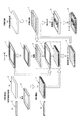
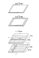
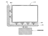
本発明の実施例を図面に沿って説明する。図1は本発明の第1の実施例を説明する図であり、(a)〜(e)に示すガラス製の固定電極基板に対して抵抗膜や電極を形成することにより製作された固定電極1と、同図(f)(g)に示す絶縁性シール材2と、同図(h)に示す可動電極用基板に電極を形成した同図(i)に示す可動電極3とを、同図(j)に示すように順に積み重ねて同図(k)に示すような狭額縁対応タッチパネル4とし、これを同図(l)に示す狭額縁のLCD5上に被せて、同図(m)に示すようなタッチパネル付LCD6とした例を示している。
Embodiments of the present invention will be described with reference to the drawings. FIG. 1 is a diagram for explaining a first embodiment of the present invention, and is a fixed electrode manufactured by forming a resistance film or an electrode on a glass fixed electrode substrate shown in FIGS. 1, the insulating sealing material 2 shown in FIGS. 1F and 1G, and the
図1(d)(e)に示す固定電極基板1の例においては、最初同図(a)〜(c)に示すように、また図2(a)〜(c)に拡大図を示すような、内部に高さh1の空間が存在する固定電極用基板11を製作する。この固定電極用基板11は従来と同様に厚さ1〜2mm程度のガラス板によって製作する。固定電極用基板11の空間の横a1、縦b1、高さh1は、図1(l)に示すLCD5の横、縦、高さと一致するように設定している。但し、LCDの高さよりも小さくしても良い。また、この固定電極用基板11の外形は高h2、横a2、縦b2としている。なお、図示の例では固定電極用基板11をガラスにより製作した例を示したが、プラスチック等により製作しても良い。
In the example of the fixed
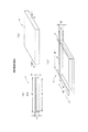
このような箱形に形成した固定電極用基板11に対して、図1(d)(e)に示すように、また図3に拡大図を示すように、表面12にはタッチパネルの抵抗膜13を形成し、図3中において右側面15は右側X電極16と、この右側電極16とスペースを介して、後述する上側面18に形成した上側Y電極回路19と接続している上側Y電極右側リード回路17を配置している。また上側面18には前記のように可動電極3に形成している上側Y電極と接続する上側Y電極回路19を配置している。
With respect to the fixed
また、図3(b)に示すように、固定電極用基板11の左側面20には、左側X電極21を形成している。更に下側面22には可動電極に形成した下側Y電極と接続している下側Y電極回路23を形成している。図3に示す例では、この下側Y電極回路23と取り出し部24とをこの下側面22において表面側から裏方向に伸びる下側Y電極リード回路25を形成している。更に下側Y電極回路23とスペースを介して、図中右半分側において、右側面15の右側X電極16と取り出し部24とを連結する右側X電極リード回路26を配置し、図中左半分側においては左側X電極21と取り出し部24とを接続する左側X電極リード回路27を配置している。なお、前記右側Y電極リード回路25と左側X電極リード回路27とは接続することなく、独立して取り出し部24に導かれている。
Further, as shown in FIG. 3B, a
更に図3に示す例においては、上側Y電極回路19と取り出し部24を接続するため、前記右側面15に配置した上側Y電極右側リード回路17と接続している上側Y電極下側リード回路28を、前記右側X電極リード回路26とはスペースを介して配置ている。なお、取り出し部24においては、各リード回路と接続するリード線を備え、制御回路に接続している。
Further, in the example shown in FIG. 3, the upper Y electrode
上記のような電極及びリード回路等を箱形の固定電極用基板11に形成するには、既に使用されている各種の三次元回路成型法の技術を採用することに製造することができる。図1(d)(e)には、このような電極及び三次元回路を形成した固定電極1を示している。
In order to form the above electrodes, lead circuits, and the like on the box-shaped fixed
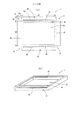
この固定電極1の表面に被せるシール材2については、図1(f)(g)に示すように、またその拡大図を図4に示すように、前記固定電極1に密着して被せることができるようにするため、固定電極1の外形高さであるh2ずつ4隅で切り落とした切り落とし部31を形成している。この切り落とし部31の角を結ぶ折曲部32で折り曲げた状態を図4(b)に示すように、厚さ0.2mm程度の絶縁材からなるシール材2は、前記のようにして形成された固定電極1の外側に配置して密着できるようにしている。
As shown in FIGS. 1 (f) and (g), and as shown in FIG. 4, an enlarged view of the sealing material 2 that covers the surface of the fixed
このシール材2の上面33には可動電極3を押下した時に可動電極3の抵抗膜が固定電極1の抵抗膜に接することができる開口34を形成している。また上側面35には、図5で後述するような可動電極3の上側内面41に形成した上側Y電極42の位置に対向し、同時に図3に示す上側Y電極回路19と対向する位置に、上側Y電極接続用溝孔36を形成している。同様にシール材2の下側面37には、図5に示す可動電極3の下側内面43に形成した下側Y電極44の位置に対向し、同時に図3に示す下側Y電極回路23に対向する位置に、下側Y電極接続用溝孔38を形成している。
An
なお、この上側Y電極接続用溝孔36及び下側Y電極接続用溝孔35には、このシール材が比較的厚い時には予め導電性ペースト等を充填しておくことにより、固定電極1にシール材2を被せ、更にその上に可動電極3を被せた時、可動電極3に形成した上側Y電極42に固定電極1に形成した上側Y電極回路19とが接続し、同時に可動電極3に形成した下側Y電極44と固定電極1に形成した下側Y電極回路23とが接続できるようにしても良い。但し、このシール材2が数μm〜数十μm程度の薄いシートの時には、特に導電性物質を用いなくても、可動電極固定時の圧力で電極と電極回路は接続可能である。
When the sealing material is relatively thick, the upper Y
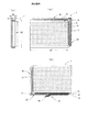
図1(i)に示す可動電極3については、前記固定電極1に対してシール材2を折り曲げて覆った後において、そのシール材2に密着して覆うことができる内部空間を備えた形状とする。この可動電極は通常のものと同様に厚さ0.2mm程度のガラス製、或いはプラスチック製とする。この可動電極3の拡大図を図5に示すように、可動電極3をガラスにより成形する時、同図(a)に示すような箱形の可動電極用部材10を製作する。この可動電極用部材10の内部空間の寸法は、固定電極1にシール材2を貼り、その上にこの可動電極3を被せた時、シール材2と密着できるような高さh3、横a3、縦b3の形状とする。
The
この可動電極3を説明する図5に示すように、その内部における上側内面41に上側Y電極42を形成し、下側内面43には下側Y電極44を形成する。この電極形成に際しては、従来と同様の三次元回路形成手法を含め各種の手法によって形成することができる。
As shown in FIG. 5 for explaining the
上記各部材の構成により例えば図1(j)に示すように、固定電極1に対して折り曲げて貼り付けた状態のシール材2に対して、更にその上に可動電極3を被せることにより、全ては一体化してタッチパネル4が製作される。なお、このような積層に際しては、適宜接着剤を用いて相互に強固に固定される。このタッチパネル4は、図1(l)に示す狭額縁のLCD5の上に被せて接着固定し、全体として図1(m)に示すようなタッチパネル付LCD6とすることができる。このような組み立てを行うことにより、タッチパネル4はLCD5上に容易に正確な位置決め状態で組み立てることができる。
As shown in FIG. 1 (j), for example, as shown in FIG. 1 (j), the sealing material 2 in a state of being bent and pasted to the fixed
上記のように、本発明の前記実施例においては、タッチパネルの電極及びリード回路等をLCDの側面部分に配置することができるので、LCDの狭額縁化に対応することができる。また、外部からの力で剥がれ易いこの部分を側面部分に配置することによって、外部からの力による損傷を防ぐこともできるようにもなる。同時に、前記のように図1(k)に示すように製作された箱形のタッチパネル4を同図(l)に示すLCD5に被せるのみで、タッチパネル付LCDを製造できるため、タッチパネルとLCDとの位置合わせを容易に且つ正確に行うことができるようになる。
As described above, in the embodiment of the present invention, the electrodes of the touch panel, the lead circuit, and the like can be arranged on the side surface portion of the LCD, so that it is possible to cope with the narrow frame of the LCD. In addition, by disposing the portion that is easily peeled off by an external force on the side surface portion, it is possible to prevent damage due to the external force. At the same time, an LCD with a touch panel can be manufactured simply by placing the box-shaped
前記実施例においては、可動電極をガラス製とすることにより、予め図5(a)〜(c)に示すような箱形の可動電極板40を製作した例を示したが、この可動電極3をプラスチック製とする時には、図4(a)のシール材と同様の形状に形成し、それに対して上側Y電極42及び下側Y電極44を形成し、これを折り曲げて固定電極1の表面に貼ったシール材2の上に被せるように製作しても良い。
In the above-described embodiment, the example in which the box-shaped movable electrode plate 40 as shown in FIGS. 5A to 5C is manufactured in advance by using the movable electrode made of glass has been described. 4 is formed in the same shape as the sealing material in FIG. 4A, the
また、前記の例においては特に低温ポリシリコンTFTを用いたLCDがガラス上にLCDドライバ用ICを作り込めるため、特に狭い額縁とすることが可能となることにより、このようなLCDに対しては前記のように、また例えば図6(a)に略示すように、両側縁46、47に突出することとなるタッチパネルについて、この部分を同図(b)に示すようにLCD5の側面部分48に配置することができるため、図示の例では両側で各々4〜7mm程度小型化することができる。このことは逆に、従来のタッチパネルを備えたLCDにおいては、この部分だけ画面を小さくしなければならなかったのに対して、タッチパネルの電極やリード回路をLCDの側面に配置することにより、例えば図6(c)に示すように広い面積の画面表示領域を形成することができ、図示の例では8〜14mm大きな画面とすることができる。このことは例えば車載機器のLCDに使用する場合のように、規定の外形寸法で比較的小型のLCDを用いる場合には特に大きな効果を生じることとなる。
Further, in the above example, an LCD using a low-temperature polysilicon TFT can make an LCD driver IC on glass, so that a particularly narrow frame can be used. As described above, for example, as schematically shown in FIG. 6A, the touch panel that protrudes from both side edges 46 and 47 is replaced with the side portion 48 of the
なお、前記のような低温ポリシリコンLCDを用いるLCDの場合以外にも、通常のアモルファスシリコンTFTを用いるLCDの場合においてもリード回路が形成されない片側の辺では狭額縁化がなされるため、例えば図6(d)のように従来片側についてはLCD5よりも突出せざるを得なかった側縁46を、同図(e)に示すようにLCD5の側面に配置することができ、したがって4〜7mm小型化することができる。この場合においても、同図(f)に示すように同じ大きさのタッチパネル付LCDにおいて、LCDの画面を大きくできることは同様である。
In addition to the LCD using the low-temperature polysilicon LCD as described above, in the case of the LCD using the normal amorphous silicon TFT, the frame on one side where the read circuit is not formed is narrowed. As shown in FIG. 6E, the
また、透過LCDにおいてバックライトが画面側方に配置される側部ライト方式の場合は、その縁は狭額縁になることはないので、図6(g)のように下側部分にバックライトが配置されている時、その部分にタッチパネルの電極やリード回路を配置できる。したがってこの場合は両側面と上部のみをLCD側部に電極等を配置するのみで良い。 Further, in the case of a side light type in which the backlight is arranged on the side of the screen in the transmissive LCD, the edge does not become a narrow frame, so that the backlight is placed on the lower part as shown in FIG. When arranged, the touch panel electrodes and lead circuits can be arranged in that portion. Therefore, in this case, it is only necessary to arrange electrodes or the like on both sides and the upper part on the LCD side.
1 固定電極
2 シール材
3 可動電極
4 タッチパネル
5 LCD
6 タッチパネル付LCD
10 可動電極用基板
11 固定電極用基板
1 fixed electrode 2
6 LCD with touch panel
10
Claims (4)
該タッチパネルの表面にはタッチ位置を検出するタッチ位置検出面を形成し、
該タッチパネルの側面には電極と該電極を外部への取り出し部に接続するリード回路とを形成し、
該タッチパネルの表面をLCDの表面に、前記側面をLCDの側部に配置させることを特徴とする狭額縁対応タッチパネル。 The touch panel is formed into a three-dimensional shape with a surface and side surfaces,
A touch position detection surface for detecting a touch position is formed on the surface of the touch panel,
On the side surface of the touch panel, an electrode and a lead circuit that connects the electrode to an outside extraction portion are formed,
A touch panel for a narrow frame, wherein the surface of the touch panel is disposed on the surface of the LCD and the side surface is disposed on the side of the LCD.
Priority Applications (1)
| Application Number | Priority Date | Filing Date | Title |
|---|---|---|---|
| JP2008324831A JP5322622B2 (en) | 2008-12-21 | 2008-12-21 | Narrow frame LCD compatible touch panel |
Applications Claiming Priority (1)
| Application Number | Priority Date | Filing Date | Title |
|---|---|---|---|
| JP2008324831A JP5322622B2 (en) | 2008-12-21 | 2008-12-21 | Narrow frame LCD compatible touch panel |
Publications (2)
| Publication Number | Publication Date |
|---|---|
| JP2010146418A true JP2010146418A (en) | 2010-07-01 |
| JP5322622B2 JP5322622B2 (en) | 2013-10-23 |
Family
ID=42566772
Family Applications (1)
| Application Number | Title | Priority Date | Filing Date |
|---|---|---|---|
| JP2008324831A Expired - Fee Related JP5322622B2 (en) | 2008-12-21 | 2008-12-21 | Narrow frame LCD compatible touch panel |
Country Status (1)
| Country | Link |
|---|---|
| JP (1) | JP5322622B2 (en) |
Cited By (9)
| Publication number | Priority date | Publication date | Assignee | Title |
|---|---|---|---|---|
| JP2012053806A (en) * | 2010-09-03 | 2012-03-15 | Kyocera Corp | Touch panel and portable communication terminal |
| WO2012132846A1 (en) * | 2011-03-31 | 2012-10-04 | 日本写真印刷株式会社 | Electrostatic capacitive touch screen |
| JP2013218648A (en) * | 2012-04-11 | 2013-10-24 | Touch Panel Kenkyusho:Kk | Touch panel structure |
| JP5347096B1 (en) * | 2012-09-13 | 2013-11-20 | 株式会社ワンダーフューチャーコーポレーション | Touch panel manufacturing method, touch panel, and input / output integrated device including touch panel and display device |
| JP2014002540A (en) * | 2012-06-18 | 2014-01-09 | Sharp Corp | Touch panel sensor and information processing device |
| WO2014087758A1 (en) * | 2012-12-06 | 2014-06-12 | 日本電気硝子株式会社 | Display device |
| KR20150106459A (en) | 2013-03-04 | 2015-09-21 | 파나쿠 가부시키가이샤 | Method for manufacturing touch panel, touch panel, method for manufacturing molded article, molded article, and laminated film |
| CN106796477B (en) * | 2015-02-27 | 2018-05-29 | 株式会社藤仓 | Wiring body, circuit board, Wiring structure body and touch sensor |
| JPWO2020195622A1 (en) * | 2019-03-25 | 2020-10-01 |
Citations (4)
| Publication number | Priority date | Publication date | Assignee | Title |
|---|---|---|---|---|
| JPS62117642U (en) * | 1986-01-11 | 1987-07-25 | ||
| JPH0292530U (en) * | 1989-01-05 | 1990-07-23 | ||
| JP2003099204A (en) * | 2001-09-26 | 2003-04-04 | Matsushita Electric Ind Co Ltd | Transparent touch panel |
| JP2006004302A (en) * | 2004-06-21 | 2006-01-05 | Nissha Printing Co Ltd | Touch panel with narrow frame |
-
2008
- 2008-12-21 JP JP2008324831A patent/JP5322622B2/en not_active Expired - Fee Related
Patent Citations (4)
| Publication number | Priority date | Publication date | Assignee | Title |
|---|---|---|---|---|
| JPS62117642U (en) * | 1986-01-11 | 1987-07-25 | ||
| JPH0292530U (en) * | 1989-01-05 | 1990-07-23 | ||
| JP2003099204A (en) * | 2001-09-26 | 2003-04-04 | Matsushita Electric Ind Co Ltd | Transparent touch panel |
| JP2006004302A (en) * | 2004-06-21 | 2006-01-05 | Nissha Printing Co Ltd | Touch panel with narrow frame |
Cited By (22)
| Publication number | Priority date | Publication date | Assignee | Title |
|---|---|---|---|---|
| JP2012053806A (en) * | 2010-09-03 | 2012-03-15 | Kyocera Corp | Touch panel and portable communication terminal |
| CN103384866B (en) * | 2011-03-31 | 2014-11-19 | 日本写真印刷株式会社 | Electrostatic capacity type touch panel |
| WO2012132846A1 (en) * | 2011-03-31 | 2012-10-04 | 日本写真印刷株式会社 | Electrostatic capacitive touch screen |
| JP5113960B2 (en) * | 2011-03-31 | 2013-01-09 | 日本写真印刷株式会社 | Capacitive touch screen |
| CN103384866A (en) * | 2011-03-31 | 2013-11-06 | 日本写真印刷株式会社 | Capacitive touch screen |
| KR101380693B1 (en) * | 2011-03-31 | 2014-04-02 | 니폰샤신인사츠가부시키가이샤 | Electrostatic capacitive touch screen |
| US9122088B2 (en) | 2011-03-31 | 2015-09-01 | Nissha Printing Co., Ltd. | Capacitance type touch screen |
| JP2013218648A (en) * | 2012-04-11 | 2013-10-24 | Touch Panel Kenkyusho:Kk | Touch panel structure |
| JP2014002540A (en) * | 2012-06-18 | 2014-01-09 | Sharp Corp | Touch panel sensor and information processing device |
| JP5347096B1 (en) * | 2012-09-13 | 2013-11-20 | 株式会社ワンダーフューチャーコーポレーション | Touch panel manufacturing method, touch panel, and input / output integrated device including touch panel and display device |
| KR20150004372A (en) | 2012-09-13 | 2015-01-12 | 가부시키가이샤 원더 퓨쳐 코포레이션 | Touch panel, method for manufacturing touch panel, and touch panel integrated display device |
| JP2014115321A (en) * | 2012-12-06 | 2014-06-26 | Nippon Electric Glass Co Ltd | Display device |
| WO2014087758A1 (en) * | 2012-12-06 | 2014-06-12 | 日本電気硝子株式会社 | Display device |
| KR20150106459A (en) | 2013-03-04 | 2015-09-21 | 파나쿠 가부시키가이샤 | Method for manufacturing touch panel, touch panel, method for manufacturing molded article, molded article, and laminated film |
| US9597858B2 (en) | 2013-03-04 | 2017-03-21 | Panac Co., Ltd. | Method for manufacturing touch panel and molded article |
| CN106796477B (en) * | 2015-02-27 | 2018-05-29 | 株式会社藤仓 | Wiring body, circuit board, Wiring structure body and touch sensor |
| US10394398B2 (en) | 2015-02-27 | 2019-08-27 | Fujikura Ltd. | Wiring body, wiring board, wiring structure, and touch sensor |
| JPWO2020195622A1 (en) * | 2019-03-25 | 2020-10-01 | ||
| WO2020195622A1 (en) * | 2019-03-25 | 2020-10-01 | 富士フイルム株式会社 | Touch panel and method for manufacturing touch panel |
| CN113316758A (en) * | 2019-03-25 | 2021-08-27 | 富士胶片株式会社 | Touch panel and manufacturing method of touch panel |
| JP7352619B2 (en) | 2019-03-25 | 2023-09-28 | 富士フイルム株式会社 | Touch panel and touch panel manufacturing method |
| CN113316758B (en) * | 2019-03-25 | 2024-11-12 | 富士胶片株式会社 | Touch panel and method for manufacturing touch panel |
Also Published As
| Publication number | Publication date |
|---|---|
| JP5322622B2 (en) | 2013-10-23 |
Similar Documents
| Publication | Publication Date | Title |
|---|---|---|
| JP5322622B2 (en) | Narrow frame LCD compatible touch panel | |
| US9709837B2 (en) | Electro-optical device and electronic equipment | |
| CN102096221B (en) | It is integrated with the liquid crystal display of touch panel | |
| US9864457B2 (en) | Display device with touch sensor | |
| JP4821877B2 (en) | Protection plate integrated liquid crystal display panel and electronic device | |
| CN102096533B (en) | Capacitive input device and detection method thereof and drive unit | |
| US9013411B2 (en) | Touch panel device having an outer edge frame body, an electro-optical device using the same, and an electronic apparatus using the same | |
| US20110134075A1 (en) | Touch panel, display, and electronic device | |
| JP6216167B2 (en) | Terminal connection structure and display device with built-in touch sensor | |
| CN107870467A (en) | Display device | |
| WO2010058495A1 (en) | Touch panel and display device using the same | |
| CN104023472A (en) | Connecting structure of electronic apparatus and display device using same | |
| JP4936936B2 (en) | Touch panel | |
| JP2008134975A (en) | Input device and its manufacturing method | |
| US9664938B2 (en) | Display device | |
| CN105319742A (en) | Liquid crystal display device conductive tape attaching structure, liquid crystal display device, and manufacturing method thereof | |
| CN105607781A (en) | Array substrate, touch panel and display device | |
| JP2008033777A (en) | Electrode substrate, method for manufacturing the same, display device and method for manufacturing the same | |
| JP5836817B2 (en) | Touch panel, display device and electronic device | |
| JP2012088599A (en) | Liquid crystal display device with touch sensor function | |
| JP4591502B2 (en) | Liquid crystal device and electronic device | |
| JP2011186623A (en) | Display device with touch panel | |
| CN110192237A (en) | Display device | |
| JP2014098825A (en) | Liquid crystal display element | |
| JP2007065855A (en) | Display device with touch panel |
Legal Events
| Date | Code | Title | Description |
|---|---|---|---|
| A621 | Written request for application examination |
Free format text: JAPANESE INTERMEDIATE CODE: A621 Effective date: 20110915 |
|
| A521 | Request for written amendment filed |
Free format text: JAPANESE INTERMEDIATE CODE: A523 Effective date: 20121106 |
|
| A977 | Report on retrieval |
Free format text: JAPANESE INTERMEDIATE CODE: A971007 Effective date: 20130514 |
|
| A131 | Notification of reasons for refusal |
Free format text: JAPANESE INTERMEDIATE CODE: A131 Effective date: 20130516 |
|
| A521 | Request for written amendment filed |
Free format text: JAPANESE INTERMEDIATE CODE: A523 Effective date: 20130621 |
|
| TRDD | Decision of grant or rejection written | ||
| A01 | Written decision to grant a patent or to grant a registration (utility model) |
Free format text: JAPANESE INTERMEDIATE CODE: A01 Effective date: 20130716 |
|
| A61 | First payment of annual fees (during grant procedure) |
Free format text: JAPANESE INTERMEDIATE CODE: A61 Effective date: 20130716 |
|
| R150 | Certificate of patent or registration of utility model |
Ref document number: 5322622 Country of ref document: JP Free format text: JAPANESE INTERMEDIATE CODE: R150 Free format text: JAPANESE INTERMEDIATE CODE: R150 |
|
| LAPS | Cancellation because of no payment of annual fees |