JP2010143818A - Silica crucible with pure and bubble-free inner crucible layer and method of making the same - Google Patents
Silica crucible with pure and bubble-free inner crucible layer and method of making the same Download PDFInfo
- Publication number
- JP2010143818A JP2010143818A JP2009254727A JP2009254727A JP2010143818A JP 2010143818 A JP2010143818 A JP 2010143818A JP 2009254727 A JP2009254727 A JP 2009254727A JP 2009254727 A JP2009254727 A JP 2009254727A JP 2010143818 A JP2010143818 A JP 2010143818A
- Authority
- JP
- Japan
- Prior art keywords
- silica
- particle layer
- layer
- melting
- silica particle
- Prior art date
- Legal status (The legal status is an assumption and is not a legal conclusion. Google has not performed a legal analysis and makes no representation as to the accuracy of the status listed.)
- Granted
Links
Images


Classifications
-
- C—CHEMISTRY; METALLURGY
- C03—GLASS; MINERAL OR SLAG WOOL
- C03B—MANUFACTURE, SHAPING, OR SUPPLEMENTARY PROCESSES
- C03B19/00—Other methods of shaping glass
- C03B19/09—Other methods of shaping glass by fusing powdered glass in a shaping mould
- C03B19/095—Other methods of shaping glass by fusing powdered glass in a shaping mould by centrifuging, e.g. arc discharge in rotating mould
-
- C—CHEMISTRY; METALLURGY
- C03—GLASS; MINERAL OR SLAG WOOL
- C03B—MANUFACTURE, SHAPING, OR SUPPLEMENTARY PROCESSES
- C03B20/00—Processes specially adapted for the production of quartz or fused silica articles, not otherwise provided for
-
- C—CHEMISTRY; METALLURGY
- C30—CRYSTAL GROWTH
- C30B—SINGLE-CRYSTAL GROWTH; UNIDIRECTIONAL SOLIDIFICATION OF EUTECTIC MATERIAL OR UNIDIRECTIONAL DEMIXING OF EUTECTOID MATERIAL; REFINING BY ZONE-MELTING OF MATERIAL; PRODUCTION OF A HOMOGENEOUS POLYCRYSTALLINE MATERIAL WITH DEFINED STRUCTURE; SINGLE CRYSTALS OR HOMOGENEOUS POLYCRYSTALLINE MATERIAL WITH DEFINED STRUCTURE; AFTER-TREATMENT OF SINGLE CRYSTALS OR A HOMOGENEOUS POLYCRYSTALLINE MATERIAL WITH DEFINED STRUCTURE; APPARATUS THEREFOR
- C30B15/00—Single-crystal growth by pulling from a melt, e.g. Czochralski method
- C30B15/10—Crucibles or containers for supporting the melt
-
- Y—GENERAL TAGGING OF NEW TECHNOLOGICAL DEVELOPMENTS; GENERAL TAGGING OF CROSS-SECTIONAL TECHNOLOGIES SPANNING OVER SEVERAL SECTIONS OF THE IPC; TECHNICAL SUBJECTS COVERED BY FORMER USPC CROSS-REFERENCE ART COLLECTIONS [XRACs] AND DIGESTS
- Y10—TECHNICAL SUBJECTS COVERED BY FORMER USPC
- Y10T—TECHNICAL SUBJECTS COVERED BY FORMER US CLASSIFICATION
- Y10T117/00—Single-crystal, oriented-crystal, and epitaxy growth processes; non-coating apparatus therefor
- Y10T117/10—Apparatus
- Y10T117/1024—Apparatus for crystallization from liquid or supercritical state
- Y10T117/1032—Seed pulling
Landscapes
- Chemical & Material Sciences (AREA)
- Engineering & Computer Science (AREA)
- Materials Engineering (AREA)
- Organic Chemistry (AREA)
- Manufacturing & Machinery (AREA)
- Crystallography & Structural Chemistry (AREA)
- Metallurgy (AREA)
- Crystals, And After-Treatments Of Crystals (AREA)
- Glass Melting And Manufacturing (AREA)
Abstract
【課題】不純物濃度が最小であり且つ気泡及び気泡成長を低減させたるつぼ内層を有するシリカるつぼを合理的なコストで作製する方法を提供する。
【解決手段】モールドキャビティに設けられるシリカ粒子を介して空気を吸引する形式のモールドキャビティにおいて、シリカるつぼを製造する方法であって、純粋なシリカ粒子層230を天然シリカ粒子層228の上部に形成し、シリカ粒子を介して空気を実質的に吸引することなく、純粋なシリカ粒子層230の少なくとも一部を溶融し、シリカを介してかなり高容量の空気を吸引しながら、任意の残留する純粋なシリカ粒子層230、及び天然シリカ粒子層228の少なくとも一部を溶融し、その後、溶融された純粋なシリカ粒子層230の少なくとも一部を昇華させる。
【選択図】図1The present invention provides a method for producing a silica crucible having a minimum impurity concentration and having a crucible inner layer with reduced bubble and bubble growth at a reasonable cost.
A method of manufacturing a silica crucible in a mold cavity of a type in which air is sucked through silica particles provided in the mold cavity, and a pure silica particle layer 230 is formed on top of a natural silica particle layer 228. Any residual pure while melting at least a portion of the pure silica particle layer 230 and substantially aspirating a fairly high volume of air through the silica without substantially aspirating the air through the silica particles. At least a part of the silica particle layer 230 and the natural silica particle layer 228 are melted, and then at least a part of the melted pure silica particle layer 230 is sublimated.
[Selection] Figure 1
Description
本発明の実施形態は包括的に、シリカるつぼ及びその製造方法に関する。より詳細には、本発明の実施形態は、高純度且つ無気泡のるつぼ内層を有するシリカるつぼ及びその製造方法に関する。 Embodiments of the present invention generally relate to silica crucibles and methods for making the same. More specifically, embodiments of the present invention relate to a silica crucible having a high purity and bubble-free crucible inner layer and a method for manufacturing the same.
単結晶シリコン材料を製造する方法として種々の方法が存在する。このようなプロセスの1つである「チョクラルスキー」(CZ)プロセスは、太陽電池用途を含む半導体用途のための単結晶シリコン材料を製造するために広範に利用されている。このCZプロセスでは、溶融シリコンが容器内に入れられ、単結晶性種結晶のチップをこの溶融シリコンに浸漬する。その後、種結晶を回転させながら「引上げる」。その結果、単結晶シリコンインゴットが溶融シリコンから成長する。 There are various methods for producing a single crystal silicon material. One such process, the “Czochralski” (CZ) process, has been widely used to produce single crystal silicon materials for semiconductor applications including solar cell applications. In the CZ process, molten silicon is placed in a container and a single crystal seed crystal chip is immersed in the molten silicon. Then, “pull up” while rotating the seed crystal. As a result, a single crystal silicon ingot grows from the molten silicon.
るつぼは、シリコンインゴットを製造するこの引上げ操作に通常使用される容器の1つである。るつぼは典型的に、引上げ操作中に溶融シリコンを含有しておくようにボウル形状で構成される。るつぼは、シリカガラス、又は石英ガラスから成り、所望量の酸素を溶融シリコンに導入すると共に、溶融シリコンが金属不純物によって汚染されるのを防ぐ。 A crucible is one of the containers commonly used for this pulling operation to produce a silicon ingot. The crucible is typically configured in a bowl shape to contain molten silicon during the pulling operation. The crucible is made of silica glass or quartz glass, introduces a desired amount of oxygen into the molten silicon, and prevents the molten silicon from being contaminated by metal impurities.
CZプロセス中、シリカガラスるつぼの内表面は典型的に溶融シリコンに溶解する。るつぼ内層内に存在するあらゆる気泡は、溶解によって溶融シリコンに対して開放される可能性があり、シリコンインゴットの単結晶構造を乱すおそれのある粒子の潜在的な原因である。したがって、るつぼは典型的には、無気泡のるつぼ内層を有するように製造される。るつぼ外層は典型的に、数多くの小さい気泡を含有して発熱要素からの放射を拡散させるように製造される。 During the CZ process, the inner surface of the silica glass crucible typically dissolves in molten silicon. Any bubbles present in the crucible inner layer can be released to the molten silicon by melting and are a potential source of particles that can disturb the single crystal structure of the silicon ingot. Thus, crucibles are typically manufactured with an air-free crucible inner layer. The outer crucible layer is typically manufactured to contain a number of small bubbles to diffuse the radiation from the heating element.
CZプロセス中のシリコンインゴットの汚染の可能性を最小限に抑えるために、るつぼ内層は可能な限り純粋でなければならない。 In order to minimize the possibility of contamination of the silicon ingot during the CZ process, the inner crucible layer should be as pure as possible.
天然石英粒子から成るシリカガラスは多くの場合、5ppm〜20ppmのAl含量を含有する。シリカガラス中のAl元素は多くの場合、Li、Ca及びNa等の正に荷電した金属不純物と会合する。したがって、Al含量の減少が、他の金属元素の濃度を最小限に抑えるのに望まれる。 Silica glass composed of natural quartz particles often contains an Al content of 5 ppm to 20 ppm. Al elements in silica glass often associate with positively charged metal impurities such as Li, Ca and Na. Therefore, a reduction in Al content is desired to minimize the concentration of other metal elements.
シリカガラスるつぼ又は石英ガラスるつぼを製造する既知の一方法は、回転式モールドの内部に、合成シリカ粒子であっても天然石英粒子であってもよいシリカ粒子をるつぼ形状に形成した後、それをシリカガラスるつぼへと溶融することである。るつぼをモールドから取り出し、機械的に仕上げ加工及び洗浄して、最終製品とする。 One known method for producing a silica glass crucible or a quartz glass crucible is to form silica particles, which may be synthetic silica particles or natural quartz particles, into a crucible shape inside a rotary mold, and then apply it. Melting into a silica glass crucible. The crucible is removed from the mold and mechanically finished and cleaned to the final product.
溶融中、シリカはるつぼ内層の内表面から昇華する。シリカは、アルミナよりも速く昇華するため、天然石英粒子を出発材料として使用する場合、アルミニウムがるつぼ内層の内表面に残る。上述のように、アルミニウムは他の金属不純物と会合する。 During melting, silica sublimes from the inner surface of the crucible inner layer. Since silica sublimes faster than alumina, when natural quartz particles are used as a starting material, aluminum remains on the inner surface of the crucible inner layer. As mentioned above, aluminum associates with other metal impurities.
特許文献1に開示される一方法は、フッ化水素酸によりるつぼ内層の表面をエッチングすることによって、るつぼ内層の内表面におけるAl含量を最小限に抑えることが認識される。しかしながらこの方法は、フッ化水素酸の使用することから見て経済的にも、また環境的にも好ましいものでもない。 It is recognized that one method disclosed in Patent Document 1 minimizes the Al content on the inner surface of the crucible inner layer by etching the surface of the inner crucible layer with hydrofluoric acid. However, this method is neither economical nor environmentally preferable in view of the use of hydrofluoric acid.
特許文献2に開示される、石英ガラスるつぼを製造する別の既知の方法は、ほとんど気泡を成長させることなく、るつぼ内層を無気泡とし、るつぼ内層の内表面におけるAl含量を減少させることが認識される。るつぼは、気泡及び気泡成長を低減させるような比較的大量の電力を使用することによって溶融され、るつぼ内層の表面上にアルミニウムリッチ層を残す。その後、アルミニウムリッチ層を研磨プロセス又はエッチングプロセスによって除去する。本方法は、CZプロセス中にほとんど気泡を成長させることのない、相対的に無気泡となり得るるつぼ内層を作製することができるが、アルミニウムリッチ層を研磨又はエッチングすることは、時間を浪費するものであり、また経済的でない。 It has been recognized that another known method for producing a quartz glass crucible disclosed in US Pat. No. 6,057,096 makes the inner crucible layer bubble-free and reduces the Al content at the inner surface of the inner crucible layer with little bubble growth. Is done. The crucible is melted by using a relatively large amount of power to reduce bubbles and bubble growth, leaving an aluminum rich layer on the surface of the inner crucible layer. Thereafter, the aluminum rich layer is removed by a polishing process or an etching process. While this method can produce a crucible inner layer that can be relatively bubble-free with little bubble growth during the CZ process, polishing or etching the aluminum-rich layer is time consuming. And not economical.
したがって、不純物濃度が最小であり且つ気泡及び気泡成長を低減させたるつぼ内層を有するシリカるつぼを合理的なコストで作製することが望ましい。 Therefore, it is desirable to produce a silica crucible having a minimum impurity concentration and having a crucible inner layer with reduced bubble and bubble growth at a reasonable cost.
すなわち、本発明の請求項1に係るシリカるつぼを製造する方法は、モールドキャビティ内のシリカ粒子を介して空気を吸引することができる形式のモールドキャビティにおいて、シリカるつぼを製造する方法であって、
前記モールドキャビティに第1のシリカ粒子層を形成すること、
前記第1のシリカ粒子層上に純粋なシリカ粒子層を形成すること、
前記シリカ粒子を介して空気を実質的に吸引することなく、前記純粋なシリカ粒子層の少なくとも一部を溶融すること、
前記シリカを介してかなり高容量の空気を吸引しながら、任意の残留する純粋なシリカ粒子層、及び前記第1のシリカ粒子層の少なくとも一部を溶融すること、及び
前記溶融された純粋なシリカ粒子層の少なくとも一部を昇華させること、
を含むことを特徴とする。
That is, the method for producing a silica crucible according to claim 1 of the present invention is a method for producing a silica crucible in a mold cavity of a type in which air can be sucked through silica particles in the mold cavity,
Forming a first silica particle layer in the mold cavity;
Forming a pure silica particle layer on the first silica particle layer;
Melting at least a portion of the pure silica particle layer without substantially sucking air through the silica particles;
Melting any remaining pure silica particle layer and at least a portion of the first silica particle layer while drawing a fairly high volume of air through the silica; and the molten pure silica Sublimating at least part of the particle layer;
It is characterized by including.
本発明の請求項2に係る方法は、前記純粋なシリカ粒子層が約1ppm未満のアルミニウムを含有することを特徴とする。
The method according to
本発明の請求項3に係る方法は、前記純粋なシリカ粒子層が約0.2ppm未満のアルミニウムを含有することを特徴とする。 The method according to claim 3 of the present invention is characterized in that the pure silica particle layer contains less than about 0.2 ppm of aluminum.
本発明の請求項4に係る方法は、前記純粋なシリカ粒子層が、約1ppm未満の金属不純物を含有する合成シリカ粒子を含むことを特徴とする。
The method according to
本発明の請求項5に係る方法は、前記純粋なシリカ粒子層の厚みが約3mm未満であり、且つ昇華された部分の厚みが約0.5mmを超えて厚いことを特徴とする。
The method according to
本発明の請求項6に係る方法は、前記純粋なシリカ粒子層の厚みが約1.5mm未満であり、且つ昇華された部分の厚みが約0.8mmを超えて厚いことを特徴とする。
The method according to
本発明の請求項7に係る方法は、前記シリカ粒子を介して空気を実質的に吸引することなく溶融される前記純粋なシリカ粒子層の部分が、実質的に均質な厚みを有することを特徴とする。 The method according to claim 7 of the present invention is characterized in that the portion of the pure silica particle layer that is melted without substantially sucking air through the silica particles has a substantially uniform thickness. And
本発明の請求項8に係る方法は、前記シリカ粒子を介して空気を実質的に吸引することなく前記純粋なシリカ粒子層の少なくとも一部を溶融することは、比較的低い溶融電力による溶融で溶融することを含むことを特徴とする。
In the method according to
本発明の請求項9に係る方法は、前記シリカを介してかなり高容量の空気を吸引しながら、任意の残留する純粋なシリカ粒子層、及び前記第1のシリカ粒子層の少なくとも一部を溶融することは、前記比較的低い溶融電力よりもかなり高い第2の溶融電力で溶融することをさらに含むことを特徴とする。 The method according to claim 9 of the present invention melts any remaining pure silica particle layer and at least a part of the first silica particle layer while sucking a considerably high volume of air through the silica. Doing further includes melting with a second melting power that is substantially higher than the relatively low melting power.
本発明の請求項10に係る方法は、前記比較的低い溶融電力が約300kVA未満であることを特徴とする。
The method according to
本発明の請求項11に係る方法は、前記比較的低い溶融電力が約200kVA未満であることを特徴とする。 The method according to claim 11 of the present invention is characterized in that the relatively low melting power is less than about 200 kVA.
本発明の請求項12に係る方法は、前記溶融された純粋なシリカ粒子層の少なくとも一部を昇華させることが、前記第2の溶融電力よりも高い第3の溶融電力で昇華させることを含むことを特徴とする。
The method according to
本発明の請求項13に係る方法は、前記第3の溶融電力が約700kVAを超えて大きいことを特徴とする。 The method according to claim 13 of the present invention is characterized in that the third melting power is greater than about 700 kVA.
本発明の請求項14に係る方法は、前記比較的低い溶融電力が約300kVA未満であり、且つ前記方法が、
前記比較的低い溶融電力を約500kVA超に上げること、及び
前記溶融電力を約500kVA超に上げる前に20秒以上、前記シリカを介して前記かなり高容量の空気を吸引すること、
をさらに含むことを特徴とする。
A method according to
Raising the relatively low melting power to greater than about 500 kVA, and drawing the fairly high volume of air through the silica for at least 20 seconds before raising the melting power to greater than about 500 kVA;
Is further included.
本発明の請求項15に係る方法は、約30秒を超える間、前記シリカ粒子を介して空気を実質的に吸引することなく、前記純粋なシリカ粒子層の少なくとも一部を溶融することをさらに含むことを特徴とする。 The method according to claim 15 of the present invention further comprises melting at least a portion of the pure silica particle layer without substantially sucking air through the silica particles for more than about 30 seconds. It is characterized by including.
本発明の請求項16に係る方法は、約60秒を超える間、前記シリカ粒子を介して空気を実質的に吸引することなく、前記純粋なシリカ粒子層の少なくとも一部を溶融することをさらに含むことを特徴とする。
The method according to
本発明の請求項17に係る方法は、前記溶融された純粋なシリカ粒子層の少なくとも一部を昇華させることが、約20秒間〜約240秒間、該溶融された純粋なシリカ粒子層の少なくとも一部を昇華させることを含むことを特徴とする。 The method according to claim 17 of the present invention is such that at least one part of the molten pure silica particle layer is sublimated for at least one of the molten pure silica particle layer for about 20 seconds to about 240 seconds. Including sublimating the part.
本発明の請求項18に係る方法は、前記溶融された純粋なシリカ粒子層の少なくとも一部を昇華させることが、約700kVAを超える溶融電力で約20秒間〜約120秒間、該溶融された純粋なシリカ粒子層の少なくとも一部を昇華させることを含むことを特徴とする。 The method according to claim 18 of the present invention is such that at least a portion of the molten pure silica particle layer is sublimated for about 20 seconds to about 120 seconds at a melting power greater than about 700 kVA. And sublimating at least a part of the silica particle layer.
本発明の請求項19に係る方法は、前記溶融された純粋なシリカ粒子層の少なくとも一部を昇華させた後に、最も内側の30マイクロメートルの該溶融された純粋なシリカ粒子層が、約20ppm未満のアルミニウムを含有することを特徴とする。 The method according to claim 19 of the present invention provides that after sublimating at least a portion of the molten pure silica particle layer, the innermost 30 micrometers of the molten pure silica particle layer is about 20 ppm. It contains less than aluminum.
本発明の請求項20に係る方法は、前記溶融された純粋なシリカ粒子層の少なくとも一部を昇華させた後に、最も内側の30マイクロメートルの該溶融された純粋なシリカ粒子層が、約4ppm未満のアルミニウムを含有し、こうして製造されるるつぼが、約2mm〜約6mmである相対的に無気泡の最内層を有することを特徴とする。 According to claim 20 of the present invention, after sublimating at least a portion of the molten pure silica particle layer, the innermost 30 micrometers of the molten pure silica particle layer is about 4 ppm. A crucible containing less aluminum and thus produced is characterized by having a relatively bubble-free innermost layer that is about 2 mm to about 6 mm.
本発明の請求項21に係る方法は、前記溶融された第2のシリカ粒子層の少なくとも一部を昇華させることが、該溶融された純粋なシリカ粒子層の一部のみを昇華させることを含むことを特徴とする。 In the method according to claim 21 of the present invention, sublimating at least a part of the melted second silica particle layer includes sublimating only a part of the melted pure silica particle layer. It is characterized by that.
本発明の請求項22に係る方法は、前記溶融された第2のシリカ粒子層の少なくとも一部を昇華させることが、該溶融された純粋なシリカ粒子層の全体を実質的に昇華させることを含むことを特徴とする。 In the method according to claim 22 of the present invention, sublimating at least a part of the melted second silica particle layer substantially sublimates the entire melted pure silica particle layer. It is characterized by including.
本発明の請求項23に係るシリカるつぼは、請求項1に記載の方法に従って製造されることを特徴とする。 A silica crucible according to claim 23 of the present invention is manufactured according to the method of claim 1.
本発明の請求項24に係る方法は、シリカガラスるつぼを製造する方法であって、
モールドキャビティ内に第1のシリカ粒子層を形成すること、
前記第1のシリカ粒子層上に第2のシリカ粒子層を形成すること、
前記第2のシリカ粒子層の少なくとも一部を第1の温度で溶融すること、
前記第1のシリカ粒子層の少なくとも一部を、前記第1の温度を超える高い第2の温度で溶融すること、及び
第1のシリカ粒子層の少なくとも一部を昇華させること、
を含むことを特徴とする。
The method according to claim 24 of the present invention is a method for producing a silica glass crucible,
Forming a first silica particle layer in the mold cavity;
Forming a second silica particle layer on the first silica particle layer;
Melting at least a portion of the second silica particle layer at a first temperature;
Melting at least a portion of the first silica particle layer at a second temperature higher than the first temperature, and sublimating at least a portion of the first silica particle layer;
It is characterized by including.
本発明の請求項25に係る方法は、前記粒子を介してガスを実質的に吸引することなく、前記第2のシリカ粒子層の少なくとも一部を溶融すること、及び
前記第1のシリカ粒子層を溶融しながら、前記粒子を介して、前記モールドキャビティの内壁に分布する孔へとガスを吸引すること、
をさらに含むことを特徴とする。
The method according to claim 25 of the present invention includes melting at least a part of the second silica particle layer without substantially sucking gas through the particles, and the first silica particle layer. Sucking gas through the particles and into the holes distributed in the inner wall of the mold cavity, while melting
Is further included.
本発明の請求項26に係る方法は、前記第2のシリカ粒子層の全体を昇華させることをさらに含むことを特徴とする。 The method according to claim 26 of the present invention is characterized by further comprising sublimating the entire second silica particle layer.
本発明の請求項27に係る方法は、前記第2のシリカ粒子層の一部のみを昇華させることをさらに含むことを特徴とする。 The method according to claim 27 of the present invention further includes sublimating only a part of the second silica particle layer.
本発明の請求項28に係る方法は、前記第2のシリカ粒子層の少なくともさらなる部分を前記第2の温度で溶融することをさらに含むことを特徴とする。 The method according to claim 28 of the present invention is further characterized by melting at least a further portion of the second silica particle layer at the second temperature.
本発明の請求項29に係るシリカるつぼは、請求項24に記載の方法に従って製造されることを特徴とする。 A silica crucible according to claim 29 of the present invention is manufactured according to the method of claim 24.
本発明の請求項30に係るシリカ層を溶融する方法は、内側シリカ層、及び該内側シリカ層よりも高い濃度の金属不純物を含有する少なくとも1つの付加的なシリカ層を溶融する方法であって、
第1の電力で前記内側シリカ層の少なくとも一部を溶融することによって、第1の溶融シリカ層を形成すること、
前記第1の電力よりも大きい第2の電力で前記少なくとも1つの付加的なシリカ層の少なくとも一部を溶融することによって、第2の溶融シリカ層を形成すること、及び
前記第1の溶融シリカ層の一部を昇華させること、
を含むことを特徴とする。
A method of melting a silica layer according to claim 30 of the present invention is a method of melting an inner silica layer and at least one additional silica layer containing a higher concentration of metal impurities than the inner silica layer. ,
Forming a first fused silica layer by melting at least a portion of the inner silica layer with a first power;
Forming a second fused silica layer by melting at least a portion of the at least one additional silica layer with a second power greater than the first power; and the first fused silica Sublimating part of the layer,
It is characterized by including.
本発明の請求項31に係る方法は、前記シリカ層を介してガスを実質的に吸引することなく、前記内側シリカ層の少なくとも一部を溶融すること、及び
前記第2の溶融シリカ層を溶融しながら、前記シリカ層を介してガスを吸引すること、
をさらに含むことを特徴とする。
The method according to claim 31 of the present invention includes melting at least a portion of the inner silica layer and substantially melting the second fused silica layer without substantially sucking gas through the silica layer. While sucking gas through the silica layer,
Is further included.
本発明の請求項32に係るシリカるつぼは、請求項30に記載の方法に従って製造されることを特徴とする。 A silica crucible according to a thirty-second aspect of the present invention is manufactured according to the method of the thirty-third aspect.
本発明の請求項32に係るシリカるつぼを製造する方法は、モールドキャビティ内のシリカ粒子を介して空気を吸引することができる形式のモールドキャビティにおいて、シリカるつぼを製造する方法であって、
前記モールドキャビティに第1のシリカ粒子層を形成すること、
前記第1のシリカ粒子層上に純粋なシリカ粒子層を形成すること、
前記シリカ粒子を介して空気を実質的に吸引することなく、比較的低い溶融電力で前記純粋なシリカ粒子層の第1の部分を溶融すること、
前記シリカ粒子を介してかなり高容量の空気を吸引しながら、比較的高い溶融電力で前記純粋なシリカ粒子層の第2の部分を溶融すること、
前記シリカを介してかなり高容量の空気を吸引しながら、前記第1のシリカ粒子層の少なくとも一部を溶融すること、及び
前記純粋なシリカ粒子層の前記溶融された第1の部分を実質的に全て昇華させること、
を含むことを特徴とする。
A method for producing a silica crucible according to claim 32 of the present invention is a method for producing a silica crucible in a mold cavity of a type capable of sucking air through silica particles in the mold cavity,
Forming a first silica particle layer in the mold cavity;
Forming a pure silica particle layer on the first silica particle layer;
Melting the first portion of the pure silica particle layer with a relatively low melting power without substantially sucking air through the silica particles;
Melting the second portion of the pure silica particle layer with a relatively high melting power while drawing a fairly high volume of air through the silica particles;
Melting at least a portion of the first silica particle layer while drawing a fairly high volume of air through the silica, and substantially substantiating the molten first portion of the pure silica particle layer. To sublimate everything,
It is characterized by including.
本発明の請求項34に係るシリカるつぼを製造する方法は、前記第1のシリカ粒子層が天然シリカ粒子層を有することを特徴とする。 The method for producing a silica crucible according to claim 34 of the present invention is characterized in that the first silica particle layer has a natural silica particle layer.
本発明の請求項35に係るシリカるつぼを製造する方法は、前記シリカ粒子を介してかなり高容量の空気を吸引しながら形成される溶融部分の厚みが約2.0mm〜約6.0mmであることを特徴とする。 In the method for producing a silica crucible according to claim 35 of the present invention, the thickness of the melted portion formed while sucking a considerably high volume of air through the silica particles is about 2.0 mm to about 6.0 mm. It is characterized by that.
本発明の請求項36に係るシリカるつぼを製造する方法は、真空焼成試験後、前記純粋なシリカ粒子層の前記溶融された第2の部分が、気泡を実質的に含まず、且つ気泡成長を実質的に示さないことを特徴とする。 In the method for producing a silica crucible according to claim 36 of the present invention, after the vacuum firing test, the melted second portion of the pure silica particle layer is substantially free of bubbles, and bubble growth is prevented. It is characterized by not being substantially shown.
本発明の請求項37に係るシリカるつぼを製造する方法は、前記るつぼ内層内のアルミニウムの濃度が約1.0ppm未満であることを特徴とする。 The method for producing a silica crucible according to claim 37 of the present invention is characterized in that the concentration of aluminum in the crucible inner layer is less than about 1.0 ppm.
本発明の請求項38に係るシリカるつぼを製造する方法は、シリカるつぼを製造する方法であって、
モールドキャビティに第1のシリカ層を形成すること、
前記第1のシリカ層上に、前記第1のシリカ層と比較して低い濃度の少なくともいくらかの不純物を含有する第2のシリカ層を形成すること、
前記第2のシリカ層の少なくとも一部を組み込む内側シリカ層を溶融すること、
前記内側シリカ層を溶融した後、残留するシリカの少なくとも一部を溶融しながら、未溶融シリカを介して空気を吸引すること、及び
前記溶融された内側シリカ層の少なくとも一部を昇華させること、
を含むことを特徴とする。
A method for producing a silica crucible according to claim 38 of the present invention is a method for producing a silica crucible,
Forming a first silica layer in the mold cavity;
Forming a second silica layer on the first silica layer containing at least some impurities at a lower concentration compared to the first silica layer;
Melting an inner silica layer incorporating at least a portion of the second silica layer;
After melting the inner silica layer, sucking air through unfused silica while melting at least a portion of the remaining silica, and sublimating at least a portion of the melted inner silica layer;
It is characterized by including.
図1は、本発明の一実施形態によるるつぼを製造することができる装置の幾分概略的な断面図である。 FIG. 1 is a somewhat schematic cross-sectional view of an apparatus capable of producing a crucible according to an embodiment of the present invention.
図1は、溶融する準備の整ったモールド内に形成されるシリカ粒子の2つの層を有するモールド112の断面である。これから説明するように、溶融プロセスは5つの段階を含む。
FIG. 1 is a cross section of a
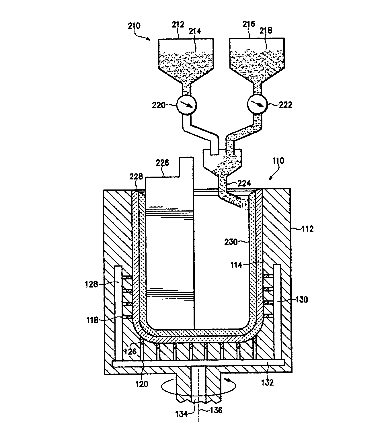
図1を参照すると、シリカガラスるつぼを製造するための装置110は、米国特許出願第11/223,158号明細書(参照により本明細書中に完全に援用される)に記載されているように提供され得る。例えば、装置110は、モールドキャビティを定める内側モールド面114を有する回転式モールド112を備え得る。
Referring to FIG. 1, an
空気路118及び空気路120のような複数の空気路が、内側モールド面114に連通している。各空気路118及び空気路120は、内側モールド面114の開口122のような円形開口を形成する円筒状の穴を有する。空気路120のような各空気路は、モールドキャビティから空気路にシリカ粒子が吸引されることを防ぐ多孔質グラファイトプラグ126を備える。空気路は、多岐管128、130、132のような多岐管に連通し、さらには穴134に連通する。排気システム501が穴134に接続している。
A plurality of air passages such as
排気システム501は、モールドキャビティから空気路を介して、最終的には穴134を介して装置110の外部に空気を吸引するように構成される。排気システムは、少なくとも開始時間及び停止時間を制御するようにプログラム可能な排気能力に関して構成される。一実施形態において、排気ポンプ502は、室内環境と通気させるリーク弁503を少なくとも備える一連の制御弁504を有する。圧力ゲージ505は排気穴134に接続されている。この圧力の読取りは、溶融前線における圧力の指標として用いられる。
The
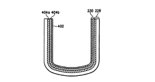
一実施形態において、モールド112は、天然石英粒子層228と、純粋なシリカ粒子層230とを含有する(内側モールド面114を露出させるように一部を取り壊したように示してある)。天然石英粒子層228及び純粋なシリカ粒子層230は、まとめて全シリカ粒子層と称することもある。
In one embodiment, the
シリカ粒子の2つの層を形成する手法を、図2A及び図2Bを用いて説明する。図2A及び図2Bは、本発明の一実施形態による供給システムを用いてシリカ粒子層を形成する方法を示す幾分概略的な断面図である。 A method of forming two layers of silica particles will be described with reference to FIGS. 2A and 2B. 2A and 2B are somewhat schematic cross-sectional views illustrating a method of forming a silica particle layer using a delivery system according to one embodiment of the present invention.
概して図2A及び図2Bを参照すると、供給システム210は、例えば、天然石英粒子214を含有する天然石英粒子ホッパー212と、純粋なシリカ粒子218を含有する純粋なシリカ粒子ホッパー216と、弁220及び弁222と、供給管224とを備え得る。モールド112の鉛直方向に出し入れ可能なスパチュラ226も備え得る。スパチュラ226はさらに、モールド112内を水平方向にも移動可能であり、モールド112が鉛直軸136の周囲を回転するにつれてシリカ粒子を成形することができる。
Referring generally to FIGS. 2A and 2B, the
一実施形態において、天然石英粒子214は、Al、Ca、Li及びK等の不純物を含有する。天然石英粒子214は、一つには、約6ppmのAl含量、約1.3ppmのCa含量、約0.7ppmのLi含量、約0.1ppmのK含量、及び約0.05ppmのNa含量を有し得る。
In one embodiment, the
一実施形態において、純粋なシリカ粒子218は、蒸留プロセスを介して精製される四塩化ケイ素から合成される。一実施形態において、純粋なシリカ粒子は1ppm未満の総金属含量を有していてもよく、このときAl含量は0.2ppm未満であり得る。
In one embodiment,
天然石英粒子ホッパー212及び純粋なシリカ粒子ホッパー216からの天然石英粒子214及び純粋なシリカ粒子218(まとめて「シリカ粒子」と称する)の流れは、それぞれ弁220及び弁222を調節することによって制御することができる。供給管224は、弁220及び弁222がどのように設定されているかに応じて、シリカ粒子の流れをホッパーのいずれか一方からモールド112に導くものである。
The flow of
図2Aを参照すると、モールド112を、約70rpm〜約150rpmの速度で鉛直軸136の周囲を回転させ、供給管224を、内側モールド面114付近に配置し、弁220を開け、天然石英粒子214の堆積を開始し、モールドキャビティの外周部に天然石英粒子層228を形成している。天然石英粒子層228の厚み(モールド112の放射軸方向で測定される)はスパチュラ226の位置によって定められる。一実施形態において、天然石英粒子層228の厚みは、約15mm〜約30mmの範囲であり得る。
Referring to FIG. 2A, the
図2Bを参照すると、天然石英粒子層228を形成した後に弁220を閉じ、モールド112を鉛直軸136の周囲に回転させながら、弁222を開ける。純粋なシリカ粒子218が、純粋なシリカ粒子ホッパー216から供給管224の外部に供給されるにつれ、純粋なシリカ粒子層230により天然石英粒子層228の内表面は被覆される。一実施形態において、純粋なシリカ粒子層230の厚みは約1mm〜約5mmの範囲であり得る。一実施形態において、天然石英粒子層228及び純粋なシリカ粒子層230の厚みを合わせた全シリカ粒子層の厚みは、約25mm〜30mmであり得る。
Referring to FIG. 2B, after the natural
純粋なシリカ粒子層230を形成した後、供給システム210及びスパチュラ226を回転式モールド112から取り出し、こうして、全シリカ粒子層を溶融してるつぼを形成することができる。
After forming the pure
図3は、本発明の一実施形態による粒子溶融システム310を用いて全シリカ粒子層を溶融する方法を示す幾分概略的な断面図である。粒子溶融システムは、プログラム可能な電源316、並びに電源に接続される電極312及び電極314を有する。本発明の一実施形態において、電源316のプログラム可能な範囲は50kVA〜1200kVAである。
FIG. 3 is a somewhat schematic cross-sectional view illustrating a method of melting an entire silica particle layer using a
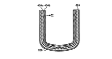
図3を参照すると、供給システム210を回転式モールド112から取り除いた後、粒子溶融システム310を回転式モールド112のキャビティに入れ、全シリカ粒子層を溶融させる。高温アークプラズマ318が全シリカ粒子層を溶融することにより、るつぼ320が形成される。るつぼ320は、天然石英粒子層228及び純粋なシリカ粒子層230(図2B中)に必ずしも対応するものでない層322及び層324を有する。層322及び層324は、むしろ、以下に記載されるプロセスにおける異なる工程の結果として形成される。示されるように、層322としては、純粋なシリカ粒子層230の一部、純粋なシリカ粒子層230の全て、又は純粋なシリカ粒子層230の全て及び天然石英粒子層230の一部が挙げられ得る。
Referring to FIG. 3, after the
排気システム501はプログラム化したように動作し、ガスが、回転式モールド112の内部から、全シリカ粒子層を介して、空気路118及び空気路120のような空気路へと吸引される。一般に、全シリカ粒子層の溶融は最内面で開始される。その後、溶融前線は、停止するまで外側へと移動し、るつぼ320と内側モールド面114との間に薄い未溶融粒子層326を残す。
The
溶融プロセスは、溶融電力、溶融前線位置、及び溶融前線における真空の変動により定められる5つの段階に分割することができる。図4A〜図4Dは、非斜線部分が未溶融粒子を示し、斜線部分が溶融された粒子の種々の層を示す、プロセスにおける連続工程を示す。5つの段階の第1の包括的な説明を、表1及び図4A〜図4Dを参照して示した後に、プロセスのより詳細な説明を表1のパラメータを用いて示す。 The melting process can be divided into five stages defined by the melting power, the position of the melting front, and the variation of the vacuum at the melting front. 4A-4D show successive steps in the process where the non-hatched portion indicates unmelted particles and the shaded portion indicates various layers of melted particles. A first comprehensive description of the five stages is given with reference to Table 1 and FIGS. 4A-4D, followed by a more detailed description of the process using the parameters in Table 1.
表1を参照すると、第1段階は皮膜形成の開始である。皮膜402は、穴134により実質的に大気圧で形成される。本発明の一実施形態において、排気システム501は、ポンプ502を運転していてもリーク弁503を大気に対し開くことによって停止している。この実施形態では、排気が皮膜の均質性に有害であり得ることから、この皮膜形成(skinning)段階において排気システム501は停止している。通常、高度な無気泡特性及び低い気泡成長特性が要求されるときには、モールドは、118及び120のような空気路を配置するように設計されている。これらの空気路は典型的にるつぼのコーナー半径部及び底部に配置される。何故ならば、形成されたるつぼをCZプロセスにおいて使用する場合は、シリコン溶融物との接触の接続は、るつぼの半径部及び底部において重要であるからである。皮膜を形成する前に排気システムを作動させると、高温プラズマガスが空気路に送られる。その結果、厚い皮膜が空気路位置に形成し、より薄い皮膜が他の場所に形成する。これは、昇華又は他の方法によって除去することが困難な不均一な厚みの皮膜を作る。また、薄い均質な皮膜は、空気路位置の溶融前線における圧力を下げることを助ける。
Referring to Table 1, the first stage is the start of film formation. The
皮膜形成位置を操作する洗練された方法の1つは、無気泡領域のために作製される空気路以外の別の一連の空気路(これらの実施形態では図示せず)を設けること、これらの空気路を介して排気させることによって皮膜形成を促進させることである。しかし、電気アークの電力及び位置を制御しながら皮膜形成中に空気路を介した空気の流れを停止させることは、均質で薄い皮膜を形成するのに実用上満足のいくものであり、また経済的である。 One sophisticated method of manipulating the film formation location is to provide another series of air passages (not shown in these embodiments) other than the air passages created for the bubble-free region, It is to promote film formation by exhausting through the air passage. However, stopping the flow of air through the air path during film formation while controlling the power and position of the electric arc is practically satisfactory for forming a homogeneous and thin film and is economical. Is.
第2段階は、皮膜の完成及び排気の開始である。粒子層の表面の大半は、皮膜402によって被覆されているため、溶融前線における圧力は、排気システム501を作動させることによってこの段階で低くなり得る。皮膜は特にモールドの上部で完全ではないため、溶融前線における圧力は、皮膜402と内側モールド面114との間の未溶融粒子を介した「漏洩」に強く関係する。
The second stage is the completion of the coating and the start of evacuation. Since most of the surface of the particle layer is covered by the
第1段階及び第2段階の間、溶融電力は、皮膜を形成するための必要最低限の値に制御する。そうでなければ、皮膜402は、後に昇華により除去することができないほど厚くなってしまう。排気システム501を作動させた後の皮膜402は、無気泡の場合があるが、CZプロセス時に気泡成長を示す。これはおそらく、低電力で溶融されたシリカガラスが十分に脱気されていないため、CZプロセスのような高温において気泡成長を示すことが原因である。一実施形態において、排気システムは、リーク弁503を閉じることによって作動する。本実施形態では、排気システムを作動させると直ぐに、溶融電力が上がる。本発明の一実施形態では、排気システムを作動させた10秒後に、溶融電力が上がる。
During the first stage and the second stage, the melting power is controlled to a minimum value necessary for forming a film. Otherwise, the
第3段階は、溶融電力を上げることによって皮膜402の下の無気泡層を溶融する。排気システム501は第2段階の終わりに作動させてある。ここで、全シリカ粒子層の上面から第1の開口までの比較的長い距離によって、流れをポンプ送りする抵抗が増大する。さらにこれは、全シリカ粒子層の上面の上の環境と多岐管128、130及び132との間の圧力低下を増大させる。結果として、溶融前線における圧力が減少し、ガスは、ポンプ502によって溶融前線から多岐管128、130及び132へと吸引される。良好な真空度を確実にする良好な皮膜被覆率に加えて、るつぼをCZプロセスに使用する際に気泡成長を減少させるように、高電力溶融が必要とされる。高電力溶融は、溶融シリカガラスの脱気を助けると推測される。一実施形態において、電極への電力を、第3段階で600kVAに増大させる。
The third stage melts the bubble-free layer under the
純粋なシリカ粒子がどれほど厚いかに応じて、無気泡層は、純粋なシリカガラスであっても、又は純粋なシリカ粒子層230から形成される純粋なシリカガラスと、天然石英粒子層228から形成される天然石英ガラスとの組み合わせであってもよい。この無気泡層はるつぼ内層322を構成する。
Depending on how thick the pure silica particles are, the bubble-free layer may be pure silica glass or formed from pure silica glass formed from pure
第4段階は、るつぼ内層322の外側の不透明なるつぼ外層324を溶融する。排気能力を下げることによって、気泡は溶融前線に誘導され得る。気泡サイズ及び気泡量を制御するために、また気泡成長を低減するために、制御された真空及び比較的高い電力がこの段階で要求される。一実施形態において、一連の制御弁504は、電極に600kVAを印加しながら、圧力ゲージ505で680Torrが維持されるように操作される。
The fourth stage melts the opaque
溶融の第5段階は上記皮膜402の除去である。皮膜402を低溶融電力で、主に大気圧で溶融するので、皮膜402は無気泡でなく、それらの気泡はCZプロセス中に成長すると考えられる。このため、この皮膜402は除去しなければならない。皮膜を除去する最良の方法は、皮膜を形成するシリカガラスの昇華である。本発明の一実施形態では、電力を、600kVAから850kVAにまで42%上げた。電力レベル及びブースト工程は、遮蔽、電源の効率及びるつぼ内部における通気等の装置の構成に応じて変更することができる。
The fifth stage of melting is removal of the
第4段階の終わりにモールド112とるつぼ320との間にいくらかの未溶融粒子326が残る飽和点で溶融前線は略停止する。
At the end of the fourth stage, the melting front almost stops at the saturation point where some
この第5段階は、或る程度の量の昇華が通常第3段階及び/又は第4段階で生じていることから、これらの段階と合わせてもよく、又はそれらの段階と重複してもよい。しかしながら、付加的な段階は皮膜を完全に除去する。第5段階は好ましくは、昇華のみを意図するものであり、溶融前線の進行が最小限に抑えられるものである。最終段階で昇華させる別の理由は、その後るつぼ内に落下し、るつぼ上に「ガス堆積(fume-deposit)」欠陥をもたらす、電極上における昇華した材料の堆積を防止するためである。第5段階、すなわち昇華段階は、皮膜の昇華後に残るアルミニウムの蓄積を最低限に抑えることが求められる。かかるアルミニウムの蓄積はより早期の段階の間に自然に発生する。皮膜の除去は、通常起こるよりも強力な昇華を必要とする。一実施形態では、0.8mm〜1.2mm厚の純粋なシリカ粒子層に対応する純粋なシリカガラスが、その後昇華される皮膜を作製するのに用いられる。この層は、図2B中の純粋なシリカ粒子層230中の粒子から溶融される。無気泡層を含む最終的なるつぼ構造体の設計、るつぼ層における純度プロファイル、粒子形成、溶融電力プログラム及び排気プログラムは、カスタマイズすることができる。
This fifth stage may be combined with or overlapping with these stages, since some amount of sublimation usually occurs in the third and / or fourth stage. . However, the additional step completely removes the coating. The fifth stage is preferably intended for sublimation only, so that the progress of the melt front is minimized. Another reason for sublimation at the final stage is to prevent the deposition of sublimated material on the electrode, which subsequently falls into the crucible and results in “fume-deposit” defects on the crucible. The fifth stage, the sublimation stage, is required to minimize the accumulation of aluminum remaining after the film sublimation. Such aluminum accumulation occurs naturally during earlier stages. Removal of the film requires more intense sublimation than normally occurs. In one embodiment, pure silica glass corresponding to a pure silica particle layer 0.8 mm to 1.2 mm thick is used to make a film that is then sublimated. This layer is melted from the particles in the pure
最内層ではより良好な封止とより良好な純度との矛盾が存在する。皮膜は厚いほど、下により良好な透明層を形成するのを助けるが、皮膜は薄いほど、皮膜を昇華させた後に残る不純物を少なくする。一実施形態では、約0.8mm〜1.2mmの純粋なシリカ粒子層を、皮膜を形成するのに用いた。昇華によって皮膜を取り去った後、この不純物プロファイルは従来技術よりも改良されていた。純粋なシリカ粒子の代わりに、天然石英粒子を皮膜に用いると、不純物プロファイルは昇華後により大きくなった。 There is a contradiction between better sealing and better purity in the innermost layer. A thicker film helps to form a better transparent layer below, while a thinner film reduces the impurities that remain after sublimating the film. In one embodiment, a pure silica particle layer of about 0.8 mm to 1.2 mm was used to form the coating. After removing the film by sublimation, this impurity profile was improved over the prior art. When natural quartz particles were used in the coating instead of pure silica particles, the impurity profile was larger after sublimation.
純粋なシリカ粒子の最内層は、皮膜形成に求められるものよりも厚いことがある。昇華後に、るつぼは、天然石英ガラス層上に無気泡且つ気泡成長のない純粋なシリカ層を有し得る。純粋なシリカ粒子の厚みに応じて、且つ排気能力を低減すると、最終的なるつぼの気泡構造体を、所望の品質及び深さに細かく制御することができる。 The innermost layer of pure silica particles may be thicker than required for film formation. After sublimation, the crucible may have a pure silica layer without bubbles and without bubble growth on the natural quartz glass layer. Depending on the thickness of the pure silica particles and reducing the exhaust capacity, the final crucible cell structure can be finely controlled to the desired quality and depth.
一実施形態では、無気泡層の内側半分が、純粋なシリカ粒子から成り、無気泡層の外側半分及び不透明外層が、天然石英ガラスから成る(図5A〜図5D)。 In one embodiment, the inner half of the bubble-free layer consists of pure silica particles, and the outer half of the bubble-free layer and the opaque outer layer consist of natural quartz glass (FIGS. 5A-5D).
るつぼ320によるCZプロセスの効果は、CZプロセスをシミュレートする真空焼成試験(vacuum bake test)を実施することによって評価することができる。例えば、真空焼成試験は、約1650℃で3時間0.1Pa圧のアルゴン雰囲気においてるつぼ片を加熱することを含み得る。
The effectiveness of the CZ process with the
本発明によるるつぼは、特に底部上及びコーナー半径部周辺において、この真空焼成試験に応じて局在的な気泡を含有する領域、又は気泡成長を示す領域を有していない。したがって、るつぼ内層322からの気泡溶解の結果として、パーティクル生成に起因し得るCZプロセス中に引き上げられたシリコンインゴットの単結晶構造中の乱れが防がれている。
The crucible according to the present invention does not have a region containing localized bubbles or a region showing bubble growth, particularly on the bottom and around the corner radius, depending on this vacuum firing test. Therefore, as a result of bubble dissolution from the crucible
上記るつぼ内層322及びるつぼ外層324を形成する例示的な方法を、図4A〜図4D及び表1を参照してここでより詳細に説明する。
An exemplary method for forming the crucible
図4A〜図4Dは、本発明の一実施形態によるるつぼ溶融プロセスの種々の段階における、るつぼを溶融する方法を示す断面図である。表1は、本発明の上記の実施形態による5つの段階の概要である。 4A-4D are cross-sectional views illustrating a method of melting a crucible at various stages of a crucible melting process according to one embodiment of the present invention. Table 1 is an overview of the five stages according to the above embodiment of the present invention.
表1中、アークへの電力はkVA単位で示している。排気能力は任意の単位で示している。値100は、800m3/時間での真空ポンプ操作による圧力ゲージ505の読取りに対応する。各段階における主な事象を表中に記載する。各段階で溶融される粒子は、溶融前線の進行の定性的な速度に沿って説明される。真空度すなわち溶融前線における圧力は、任意単位を用いて示される。圧力は全溶融前線に関して均質でないため、数値は相対的な数値として理解される。下端において、値5は圧力ゲージ505におけるおおよその大気圧であり、値100は圧力ゲージ505において約150Torrである。昇華量及び補足も表に示している。
In Table 1, the power to the arc is shown in units of kVA. The exhaust capacity is shown in arbitrary units. A value of 100 corresponds to a
図4A及び表1を参照すると、るつぼ溶融プロセスの第1段階において、最内面の純粋なシリカ粒子層230の一部が溶融し、皮膜層402が形成される。第1段階中、電極312及び電極314に印加される電力は約100kVA以下であり得る。一実施形態において、電極312及び電極314に印加される電力は、約40kVA〜約80kVAの範囲であってもよい。第1段階中、排気システム501は、圧力ゲージ505で測定される圧力が約760Torrであるように停止され得る。
Referring to FIG. 4A and Table 1, in the first stage of the crucible melting process, a portion of the innermost pure
この条件は、皮膜が最終的なるつぼ形状の略80%を占める第2段階へと継続される。皮膜層402の大部分は、排気されずに溶融することによって形成されるため、皮膜層402は気泡を含有し得る。皮膜層402は、比較的低い電力で溶融することによって形成されるため、皮膜層はまたCZプロセスにおいて気泡成長を示す可能性がある。
This condition continues to the second stage, where the coating accounts for approximately 80% of the final crucible shape. Since most of the
第2段階の終わりに、排気システム501を作動させる。一実施形態では、第1段階及び第2段階の間、穴134を介してガスを排気しないようにリーク弁503を大気に対し開き、ポンプ502を運転させた状態に維持していた。例えば、排気システムを作動させた後、圧力ゲージ505で測定される圧力を150Torrにまで落としてもよい。
At the end of the second stage, the
次に図4B及び表1を参照すると、るつぼ溶融プロセスの第3段階において、天然石英粒子層228である、形成された全シリカ粒子層の残部を溶融し、無気泡溶融シリカ層404aを形成する。第3段階中、電極312及び電極314に印加される電力は約600kVAであり得る。排気システム501は、天然石英ガラス層404aが実質的に気泡を含有しないことを確実にするために、運転状態に維持する。一実施形態において、第3段階の期間は、図4A〜図4Dの場合の404aと同じるつぼ内層322が、約2.0mm〜約6.0mmの厚みを有することを確実にするのに十分な時間に対応し得る。ポンプ502を第3段階の間動作させて、米国特許出願第11/223,158号明細書(参照により本明細書中に完全に援用される)に記載されるような流量でガスを排気し、るつぼ内層322を形成することができることが理解されよう。
Next, referring to FIG. 4B and Table 1, in the third stage of the crucible melting process, the remaining part of the formed silica particle layer, which is the natural
皮膜層402はいくらか第3段階中に昇華されることがあるが、その量は相対的に少ない。
The
次に図4C及び表1を参照すると、るつぼ溶融プロセスの第4段階は、この場合は天然石英粒子層である全シリカ粒子層の残部を溶融して、不透明なるつぼ外層324を形成することである。図4A〜図4Dの場合、不透明な天然石英ガラス層はるつぼ外層324を構成する。排気能力は、十分量の気泡を誘導するように低減されるが、米国特許出願第11/223,158号明細書に記載されるように、溶融電力は、CZプロセス中の気泡成長を低減するのに十分に大きいと想定される。第4段階の終わりに、内側からの電気アークによる加熱と、モールドの冷壁との接触による冷却との間の均衡点で溶融前線は略停止する。本発明の一実施形態では、電力が取り除かれると、溶融前線は略停止し、溶融したるつぼ320と内側モールド面114との間に2mm〜3mmの未溶融粒子326が残る。
Referring now to FIG. 4C and Table 1, the fourth stage of the crucible melting process is to melt the remainder of the total silica particle layer, in this case the natural quartz particle layer, to form an opaque crucible
次に図4D及び表1を参照すると、るつぼ溶融プロセスの第5段階は、皮膜402を昇華により除去することである。溶融電力は、全シリカ粒子層を標的範囲に溶融するためではなく、主に皮膜402の昇華のために印加される。一実施形態において、電極312及び電極314に印加される電力は850kVAであった。
Referring now to FIG. 4D and Table 1, the fifth stage of the crucible melting process is to remove the
内層404aから皮膜層402が除去されると、約0.1mm〜約2.0mmの純粋なシリカガラスが昇華し、皮膜層402が十分に除去されることを確実にし得る。一実施形態では、約0.6mmの純粋な溶融シリカ層402が昇華し、皮膜層402が十分に除去されることを確実にし得る。一実施形態において、るつぼ内層322は、皮膜402の除去後に約2.0mm〜約6.0mmの厚みを有する。
When the
表1と共に図4A〜図4Dにおいて例示的に上に記載されるプロセスに従って、純粋なシリカ粒子を主に皮膜に使用し、後に昇華させ、天然石英ガラスに類似のるつぼ内層(crucible inner layer)322の最内面を残す。図6は、本発明の一実施形態におけるるつぼ内層322上の不純物プロファイルを示す。約30マイクロメートル厚を有する3つの連続する表層をエッチングにより除去し、分析した。最内層は、14ppmのAl、0.2ppmのCa、0.6ppmのLi、及び0.14ppm未満のKであった。
According to the process described above in Table 4A-4D in conjunction with Table 1, pure silica particles were used primarily in the coating and later sublimated to provide a crucible
天然石英粒子純度と同様の純度を有する最内面についてこれは自明でないことを理解されたい。純度は表4に示される従来方法の比較例よりもさらに1桁良好であることが理解される。これは、表4及び図8による比較例としてより詳細に後に説明される。 It should be understood that this is not obvious for the innermost surface having a purity similar to that of natural quartz particles. It can be seen that the purity is an order of magnitude better than the comparative example of the conventional method shown in Table 4. This will be explained later in more detail as a comparative example according to Table 4 and FIG.
本発明の別の実施形態を、表2に伴う図5A〜図5Dに示す。図5Aに示されるような形成される粒子層は、図4Aに示されるこれまでの事例とは異なる。純粋なシリカ粒子層230は、皮膜に要求されるものよりも厚い。第3段階で溶融される無気泡層は、図5Bに示されるように純粋なシリカ粒子層230及び天然石英粒子層228から溶融する。通常、るつぼは、CZプロセス中に溶解される層よりも厚い無気泡層を有する。経済的な解決策として、無気泡層は、純粋なシリカ層404b及び天然石英ガラス層404aを有するように設計される。
Another embodiment of the present invention is shown in FIGS. The formed particle layer as shown in FIG. 5A is different from the previous case shown in FIG. 4A. The pure
不透明なるつぼ外層324は、図4Cに示されるのと同様に図5Cに示すように溶融される。
The opaque crucible
図5Dは溶融プロセスの完了図である。表2に示されるように処理されるるつぼは、るつぼ内層322の内側部分として純粋なシリカ無気泡層を有する。一実施形態において、純粋なシリカ粒子は、Al、Ca、Li、Na及びKの全てに関して0.2ppm未満で形成された。約30マイクロメートル厚の最内面層は、2ppmのAl、0.2ppmのCa、0.5ppmのLi及び0.1ppm未満のKを有していた。3つの層分析によって観測される不純物プロファイルを図7に示す。観測される不純物の増大は、天然石英ガラス層404aからの拡散に起因し得ると思われる。
FIG. 5D is a completion diagram of the melting process. The crucible treated as shown in Table 2 has a pure silica bubble free layer as the inner part of the crucible
一比較例を図には示さず表3に示す。排気システムは、第1段階の開始時から動作させる。局在的な皮膜が、真空焼成試験により、表面の非常に近くで気泡成長を示す局在的な領域として観測された。この気泡成長層は、主要な排気開口が配置されるコーナー半径部で観測される。るつぼを、CZプロセスに用いると、結晶引上げの終了に向かって構造欠損を示す好ましくない結果が示された。 One comparative example is shown in Table 3, not shown in the figure. The exhaust system is operated from the beginning of the first stage. A localized coating was observed as a localized region showing bubble growth very close to the surface by a vacuum firing test. This bubble growth layer is observed at the corner radius where the main exhaust openings are arranged. The use of crucibles in the CZ process showed undesirable results indicating structural defects towards the end of crystal pulling.
表4は、例えば米国特許出願第11/223,158号明細書に記載されるようなるつぼを製造する従来の既知の方法を示す。 Table 4 shows prior known methods for producing crucibles such as those described in US patent application Ser. No. 11 / 223,158.
純粋なシリカ粒子層は形成されない。直径及び厚みに関する寸法が得られた後に溶融プロセスが完了した。600kVAの電力は、所望の寸法を得るのに十分なものであった。真空焼成試験の結果、最内面の薄層は気泡成長を示した。30マイクロメートル厚のるつぼの内表面を分析すると、110ppmのAl、1.8ppmのCa、1.3ppmのLi及び0.1ppmのKが示された。このるつぼの不純物プロファイルを図8に示す。 A pure silica particle layer is not formed. The melt process was completed after dimensions related to diameter and thickness were obtained. The 600 kVA power was sufficient to obtain the desired dimensions. As a result of the vacuum firing test, the innermost thin layer showed bubble growth. Analysis of the inner surface of a 30 micrometer thick crucible showed 110 ppm Al, 1.8 ppm Ca, 1.3 ppm Li and 0.1 ppm K. The impurity profile of this crucible is shown in FIG.
図6、図7及び図8はそれぞれ、るつぼA、るつぼB及びるつぼDの各々の最内壁内の不純物のグラフから成る。各グラフのL1データ点は、るつぼ最内層を30マイクロメートルの深さまでエッチングし且つそのエッチング溶液を分析することによって定められる。L2データ点は、さらなる30マイクロメートルをさらにエッチングし且つそのエッチング溶液を分析することによって定められ、L3データ点は、さらなる30マイクロメートルをさらにエッチングし且つ分析することから得られる。 6, 7 and 8 comprise graphs of impurities in the innermost walls of each of crucible A, crucible B and crucible D, respectively. The L1 data point in each graph is determined by etching the inner crucible layer to a depth of 30 micrometers and analyzing the etching solution. The L2 data point is determined by further etching an additional 30 micrometers and analyzing the etching solution, and the L3 data point is obtained by further etching and analyzing an additional 30 micrometers.
図9は、示される不純物プロファイルを作成するのに使用される最内層1001、層1001を含む純粋なシリカ層1002、層1001及び層1002を含む無気泡且つ気泡成長が遅い層1003、並びに層1003とるつぼの径方向の外面1005との間に広がる気泡を含む不透明層1004を備えるコアサンプルである。サンプルの下のグラフは、表4に記載されるるつぼDに関するもの、及び表2に記載されるるつぼBに関するものの2つの異なるプロセスに関するるつぼの壁中のアルミニウムを示す。るつぼDをCZプロセスに使用すると、引上げを開始する際に困難が生じた。引上げを開始するには何回かの再試行が必要であった。
FIG. 9 shows an
実施例1
天然石英粒子を、回転式モールドにおいて天然粒子層として形成した。厚みが3.5mmの合成シリカ粒子を、天然石英粒子層上に純粋なシリカ粒子層として形成した。合成シリカ粒子は、Al、Ca、Li、Na及びKをそれぞれ0.2ppm未満で含有していた。天然石英粒子は、6ppmのAl、1.3ppmのCa、0.7ppmのLi、0.05ppmのNa及び0.1ppmのKを有していた。
Example 1
Natural quartz particles were formed as natural particle layers in a rotary mold. A synthetic silica particle having a thickness of 3.5 mm was formed as a pure silica particle layer on the natural quartz particle layer. The synthetic silica particles contained Al, Ca, Li, Na and K at less than 0.2 ppm each. The natural quartz particles had 6 ppm Al, 1.3 ppm Ca, 0.7 ppm Li, 0.05 ppm Na and 0.1 ppm K.
回転式モールドは、直径463mmのキャビティを有していた。1000kVAのプログラム可能なDC電源をグラファイト電極に接続した。排気システムは800m3/時間の排気性能、並びに排気能力を制御するための一連の弁及び配管を有していた。 The rotary mold had a cavity with a diameter of 463 mm. A 1000 kVA programmable DC power supply was connected to the graphite electrode. The exhaust system had an exhaust performance of 800 m 3 / hour, as well as a series of valves and piping to control the exhaust capacity.
溶融プログラムの5つの工程を、表2に示すように操作した。 The five steps of the melting program were operated as shown in Table 2.
第1段階及び第2段階は合計して2分かかった。排気システムを、リーク弁を開けることによって停止し、(弁を閉じることによって)1分50秒で作動させる。第1段階及び第2段階における電力は60kVA〜100kVAであった。排気穴134によって位置決めされる真空センサを用いて、溶融前線における圧力をモニタリングした。読取りは、溶融前線における圧力を示すものではないが、相対値を示す。第3段階における圧力の読取りは150Torrであった。第3段階及び第4段階で電力を100kVAから600kVAに上げた。第4段階では、排気システムはセンサ位置で680Torrに調整された。
The first and second stages took a total of 2 minutes. The exhaust system is stopped by opening the leak valve and is activated (by closing the valve) in 1
第5段階において、電力を850kVAに上げると、大規模なヒューム生成が観測された。 In the fifth stage, when the power was increased to 850 kVA, large-scale fume generation was observed.
冷却後、溶融部をモールドから取り出し、所要の高さに切断した。外径は、11.5mmの壁厚を有して457mmであった。 After cooling, the melted part was taken out from the mold and cut to a required height. The outer diameter was 457 mm with a wall thickness of 11.5 mm.
或るるつぼは、切断して真空焼成試験用の切取試片とした。およそ1650℃で約3時間、約0.1Pa圧のアルゴンで、るつぼを焼成する真空焼成試験を実施した後、るつぼが、気泡を実質的に含まず且つ顕著な気泡成長を示さない3.5mm厚のるつぼ内層を有することが確認された。 A certain crucible was cut into a cut specimen for a vacuum firing test. After performing a vacuum firing test in which the crucible is fired at about 1650 ° C. for about 3 hours with argon at a pressure of about 0.1 Pa, the crucible is substantially free of bubbles and exhibits no significant bubble growth. It was confirmed to have a thick crucible inner layer.
約30μmのるつぼ内層を分析のために溶解した。3つの連続層を分析した。濃度プロファイルを図7に示す。 The inner crucible layer of about 30 μm was dissolved for analysis. Three consecutive layers were analyzed. The density profile is shown in FIG.
結晶構造に関する如何なる問題も伴うことなくるつぼはCZプロセスに用いられた。 The crucible was used in the CZ process without any problems with the crystal structure.
実施例2
1.5mm厚の合成シリカ粒子層を天然石英粒子層上に形成した以外は、実施例1に概説したものと同様の手順に従ってるつぼを調製した。
Example 2
A crucible was prepared following the same procedure as outlined in Example 1 except that a 1.5 mm thick synthetic silica particle layer was formed on the natural quartz particle layer.
溶融プログラムの5つの工程は、表1、そうでなければ同様の実施例1に示すように操作した。 The five steps of the melting program were operated as shown in Table 1, otherwise similar to Example 1.
図6に示すように不純物プロファイルを明らかにするために3つの最内層を分析した。最内層である層L1の純度は実施例1ほど純粋ではないが、以下の比較例よりも1桁良好である。 The three innermost layers were analyzed to reveal the impurity profile as shown in FIG. The purity of the innermost layer L1 is not as pure as Example 1, but is one order of magnitude better than the following comparative examples.
このるつぼは、構造欠損に関して同様に良好に機能した。シリコン溶融物は、実施例1の場合よりも多くの不純物を有するとされるが、構造欠損に対して重要なものではなかった。 This crucible worked equally well with respect to structural defects. Although the silicon melt is said to have more impurities than in the case of Example 1, it was not important for structural defects.
比較例1
表3に示すように溶融段階をとった以外は、実施例1に概説したものと同様の手順に従ってるつぼを調製した。最大の違いは、排気システムを第1段階の始めから作動させたことである。
Comparative Example 1
A crucible was prepared according to a procedure similar to that outlined in Example 1 except that the melting stage was taken as shown in Table 3. The biggest difference is that the exhaust system was activated from the beginning of the first stage.
真空焼成試験結果から、コーナーR周辺に気泡層が示され、これは皮膜が完全に除去されていなかったことを示した。 From the results of the vacuum firing test, a bubble layer was shown around the corner R, indicating that the film was not completely removed.
このるつぼをCZプロセスに使用したが、単結晶の引上げの開始が成功する前に、3回の試行が繰り返し必要であった。 This crucible was used for the CZ process, but three trials were required repeatedly before the start of pulling of the single crystal was successful.
比較例2
合成シリカ粒子層を天然石英粒子層上に形成しなかったこと以外は、実施例1に概説したものと同様の手順に従ってるつぼを調製した。溶融段階は表4に示した通りである。意図的な昇華のための第5段階はない。所要の寸法、直径及び壁厚を満たした時点で溶融を停止した。不純物プロファイルは図8に示す。実に、850kVA等の高電力における昇華段階がないため、莫大な不純物の集積が観測された。第1の層L1中のアルミニウム含量は、実施例2よりも7.8倍大きく且つ実施例1よりも55倍大きい110ppmであった。
Comparative Example 2
A crucible was prepared according to a procedure similar to that outlined in Example 1 except that no synthetic silica particle layer was formed on the natural quartz particle layer. The melting stage is as shown in Table 4. There is no fifth stage for intentional sublimation. When the required dimensions, diameter and wall thickness were met, melting was stopped. The impurity profile is shown in FIG. Indeed, since there was no sublimation stage at high power such as 850 kVA, a huge accumulation of impurities was observed. The aluminum content in the first layer L1 was 110 ppm which was 7.8 times greater than Example 2 and 55 times greater than Example 1.
このるつぼに関して、成功したCZ引上げは70%未満であった。成功した引上げにすら、その引上げを終了するのに数回の再試行が必要であった。 For this crucible, the successful CZ pull-up was less than 70%. Even a successful pull would require several retries to finish the pull.
Claims (38)
前記モールドキャビティに第1のシリカ粒子層を形成すること、
前記第1のシリカ粒子層上に純粋なシリカ粒子層を形成すること、
前記シリカ粒子を介して空気を実質的に吸引することなく、前記純粋なシリカ粒子層の少なくとも一部を溶融すること、
前記シリカを介してかなり高容量の空気を吸引しながら、任意の残留する純粋なシリカ粒子層、及び前記第1のシリカ粒子層の少なくとも一部を溶融すること、及び
前記溶融された純粋なシリカ粒子層の少なくとも一部を昇華させること、
を含む、シリカるつぼを製造する方法。 A method of manufacturing a silica crucible in a mold cavity of a type capable of drawing air through silica particles in the mold cavity, comprising:
Forming a first silica particle layer in the mold cavity;
Forming a pure silica particle layer on the first silica particle layer;
Melting at least a portion of the pure silica particle layer without substantially sucking air through the silica particles;
Melting any remaining pure silica particle layer and at least a portion of the first silica particle layer while drawing a fairly high volume of air through the silica; and the molten pure silica Sublimating at least part of the particle layer;
A method for producing a silica crucible, comprising:
前記比較的低い溶融電力を約500kVA超に上げること、及び
前記溶融電力を約500kVA超に上げる前に20秒以上、前記シリカを介して前記かなり高容量の空気を吸引すること、
をさらに含む、請求項8に記載の方法。 The relatively low melting power is less than about 300 kVA, and the method comprises:
Raising the relatively low melt power to greater than about 500 kVA, and drawing the fairly high volume of air through the silica for 20 seconds or more before raising the melt power to greater than about 500 kVA;
The method of claim 8, further comprising:
モールドキャビティ内に第1のシリカ粒子層を形成すること、
前記第1のシリカ粒子層上に第2のシリカ粒子層を形成すること、
前記第2のシリカ粒子層の少なくとも一部を第1の温度で溶融すること、
前記第1のシリカ粒子層の少なくとも一部を、前記第1の温度を超える高い第2の温度で溶融すること、及び
第1のシリカ粒子層の少なくとも一部を昇華させること、
を含む、シリカガラスるつぼを製造する方法。 A method for producing a silica glass crucible, comprising:
Forming a first silica particle layer in the mold cavity;
Forming a second silica particle layer on the first silica particle layer;
Melting at least a portion of the second silica particle layer at a first temperature;
Melting at least a portion of the first silica particle layer at a second temperature higher than the first temperature, and sublimating at least a portion of the first silica particle layer;
A method for producing a silica glass crucible, comprising:
前記第1のシリカ粒子層を溶融しながら、前記粒子を介して、前記モールドキャビティの内壁に分布する孔へとガスを吸引すること、
をさらに含む、請求項24に記載の方法。 Melting at least a portion of the second silica particle layer without substantially sucking gas through the particles, and melting the first silica particle layer, through the particles, Sucking gas into the holes distributed in the inner wall of the mold cavity;
25. The method of claim 24, further comprising:
第1の電力で前記内側シリカ層の少なくとも一部を溶融することによって、第1の溶融シリカ層を形成すること、
前記第1の電力よりも大きい第2の電力で前記少なくとも1つの付加的なシリカ層の少なくとも一部を溶融することによって、第2の溶融シリカ層を形成すること、及び
前記第1の溶融シリカ層の一部を昇華させること、
を含む、シリカ層を溶融する方法。 A method of melting an inner silica layer and at least one additional silica layer containing a higher concentration of metal impurities than the inner silica layer, comprising:
Forming a first fused silica layer by melting at least a portion of the inner silica layer with a first power;
Forming a second fused silica layer by melting at least a portion of the at least one additional silica layer with a second power greater than the first power; and the first fused silica Sublimating part of the layer,
A method for melting a silica layer, comprising:
前記第2の溶融シリカ層を溶融しながら、前記シリカ層を介してガスを吸引すること、
をさらに含む、請求項30に記載の方法。 Melting at least a portion of the inner silica layer without substantially sucking the gas through the silica layer; and melting the gas through the silica layer while melting the second fused silica layer. Sucking,
32. The method of claim 30, further comprising:
前記モールドキャビティに第1のシリカ粒子層を形成すること、
前記第1のシリカ粒子層上に純粋なシリカ粒子層を形成すること、
前記シリカ粒子を介して空気を実質的に吸引することなく、比較的低い溶融電力で前記純粋なシリカ粒子層の第1の部分を溶融すること、
前記シリカ粒子を介してかなり高容量の空気を吸引しながら、比較的高い溶融電力で前記純粋なシリカ粒子層の第2の部分を溶融すること、
前記シリカを介してかなり高容量の空気を吸引しながら、前記第1のシリカ粒子層の少なくとも一部を溶融すること、及び
前記純粋なシリカ粒子層の前記溶融された第1の部分を実質的に全て昇華させること、
を含む、シリカるつぼを製造する方法。 A method of manufacturing a silica crucible in a mold cavity of a type capable of drawing air through silica particles in the mold cavity, comprising:
Forming a first silica particle layer in the mold cavity;
Forming a pure silica particle layer on the first silica particle layer;
Melting the first portion of the pure silica particle layer with a relatively low melting power without substantially sucking air through the silica particles;
Melting the second portion of the pure silica particle layer with a relatively high melting power while drawing a fairly high volume of air through the silica particles;
Melting at least a portion of the first silica particle layer while drawing a fairly high volume of air through the silica, and substantially substantiating the molten first portion of the pure silica particle layer. To sublimate everything,
A method for producing a silica crucible, comprising:
モールドキャビティに第1のシリカ層を形成すること、
前記第1のシリカ層上に、前記第1のシリカ層と比較して低い濃度の少なくともいくらかの不純物を含有する第2のシリカ層を形成すること、
前記第2のシリカ層の少なくとも一部を組み込む内側シリカ層を溶融すること、
前記内側シリカ層を溶融した後、残留するシリカの少なくとも一部を溶融しながら、未溶融シリカを介して空気を吸引すること、及び
前記溶融された内側シリカ層の少なくとも一部を昇華させること、
を含む、シリカるつぼを製造する方法。 A method for producing a silica crucible, comprising:
Forming a first silica layer in the mold cavity;
Forming a second silica layer on the first silica layer containing at least some impurities at a lower concentration compared to the first silica layer;
Melting an inner silica layer incorporating at least a portion of the second silica layer;
After melting the inner silica layer, sucking air through unfused silica while melting at least a portion of the remaining silica, and sublimating at least a portion of the melted inner silica layer;
A method for producing a silica crucible, comprising:
Applications Claiming Priority (4)
| Application Number | Priority Date | Filing Date | Title |
|---|---|---|---|
| US13940508P | 2008-12-19 | 2008-12-19 | |
| US61/139,405 | 2008-12-19 | ||
| US12/370,517 | 2009-02-12 | ||
| US12/370,517 US8272234B2 (en) | 2008-12-19 | 2009-02-12 | Silica crucible with pure and bubble free inner crucible layer and method of making the same |
Related Child Applications (3)
| Application Number | Title | Priority Date | Filing Date |
|---|---|---|---|
| JP2013151663A Division JP5686861B2 (en) | 2008-12-19 | 2013-07-22 | Silica crucible having pure and bubble-free crucible inner layer and method for producing the same |
| JP2013151660A Division JP5670519B2 (en) | 2008-12-19 | 2013-07-22 | Method for producing a silica crucible having a pure and bubble-free crucible inner layer |
| JP2013151667A Division JP5686862B2 (en) | 2008-12-19 | 2013-07-22 | Method for producing a silica crucible having a pure and bubble-free crucible inner layer |
Publications (2)
| Publication Number | Publication Date |
|---|---|
| JP2010143818A true JP2010143818A (en) | 2010-07-01 |
| JP5489330B2 JP5489330B2 (en) | 2014-05-14 |
Family
ID=41600757
Family Applications (4)
| Application Number | Title | Priority Date | Filing Date |
|---|---|---|---|
| JP2009254727A Active JP5489330B2 (en) | 2008-12-19 | 2009-11-06 | Method for producing a silica crucible having a pure and bubble-free crucible inner layer |
| JP2013151663A Active JP5686861B2 (en) | 2008-12-19 | 2013-07-22 | Silica crucible having pure and bubble-free crucible inner layer and method for producing the same |
| JP2013151660A Active JP5670519B2 (en) | 2008-12-19 | 2013-07-22 | Method for producing a silica crucible having a pure and bubble-free crucible inner layer |
| JP2013151667A Active JP5686862B2 (en) | 2008-12-19 | 2013-07-22 | Method for producing a silica crucible having a pure and bubble-free crucible inner layer |
Family Applications After (3)
| Application Number | Title | Priority Date | Filing Date |
|---|---|---|---|
| JP2013151663A Active JP5686861B2 (en) | 2008-12-19 | 2013-07-22 | Silica crucible having pure and bubble-free crucible inner layer and method for producing the same |
| JP2013151660A Active JP5670519B2 (en) | 2008-12-19 | 2013-07-22 | Method for producing a silica crucible having a pure and bubble-free crucible inner layer |
| JP2013151667A Active JP5686862B2 (en) | 2008-12-19 | 2013-07-22 | Method for producing a silica crucible having a pure and bubble-free crucible inner layer |
Country Status (4)
| Country | Link |
|---|---|
| US (1) | US8272234B2 (en) |
| EP (1) | EP2199262B1 (en) |
| JP (4) | JP5489330B2 (en) |
| KR (1) | KR20100071907A (en) |
Cited By (4)
| Publication number | Priority date | Publication date | Assignee | Title |
|---|---|---|---|---|
| CN103635614A (en) * | 2011-04-25 | 2014-03-12 | 康宁股份有限公司 | Vessels for molten semiconducting materials and methods of making the same |
| WO2015001592A1 (en) | 2013-06-30 | 2015-01-08 | 株式会社Sumco | Method for evaluating suitability of silica powder for manufacturing of silica-glass crucible for pulling silicon single crystal |
| KR20200076636A (en) | 2018-12-19 | 2020-06-29 | 가부시키가이샤 사무코 | Quartz glass crucible |
| JP2021165213A (en) * | 2020-04-06 | 2021-10-14 | 信越石英株式会社 | Molded plate, quartz glass crucible manufacturing equipment and quartz glass crucible manufacturing method |
Families Citing this family (9)
| Publication number | Priority date | Publication date | Assignee | Title |
|---|---|---|---|---|
| JP5377930B2 (en) * | 2008-10-31 | 2013-12-25 | 株式会社Sumco | Method for producing quartz glass crucible for pulling silicon single crystal |
| JP4922355B2 (en) * | 2009-07-15 | 2012-04-25 | 信越石英株式会社 | Silica container and method for producing the same |
| US9003832B2 (en) * | 2009-11-20 | 2015-04-14 | Heraeus Shin-Etsu America, Inc. | Method of making a silica crucible in a controlled atmosphere |
| JP5500684B2 (en) * | 2010-06-25 | 2014-05-21 | 株式会社Sumco | Silica glass crucible and method for producing the same, and method for producing silicon ingot |
| FR2963341B1 (en) * | 2010-07-27 | 2013-02-22 | Saint Gobain Quartz Sas | POLYGONAL OPENING CUP |
| US9216923B2 (en) * | 2011-07-25 | 2015-12-22 | Shin-Etsu Quartz Products Co., Ltd. | Metal and graphite mold and method of making a crucible |
| US8524319B2 (en) * | 2011-11-18 | 2013-09-03 | Memc Electronic Materials, Inc. | Methods for producing crucibles with a reduced amount of bubbles |
| US8857214B2 (en) | 2011-11-18 | 2014-10-14 | Sunedison Semiconductor Limited | Methods for producing crucibles with a reduced amount of bubbles |
| JP6135982B2 (en) * | 2013-01-17 | 2017-05-31 | 日本電産株式会社 | motor |
Citations (2)
| Publication number | Priority date | Publication date | Assignee | Title |
|---|---|---|---|---|
| JP2004262690A (en) * | 2003-02-28 | 2004-09-24 | Shinetsu Quartz Prod Co Ltd | Method for producing quartz glass crucible for pulling silicon single crystal and quartz glass crucible produced by the method |
| WO2009122936A1 (en) * | 2008-03-31 | 2009-10-08 | ジャパンスーパークォーツ株式会社 | Quartz glass crucible and process for producing the same |
Family Cites Families (46)
| Publication number | Priority date | Publication date | Assignee | Title |
|---|---|---|---|---|
| GB1289737A (en) | 1969-02-26 | 1972-09-20 | ||
| DE3014311C2 (en) * | 1980-04-15 | 1982-06-16 | Heraeus Quarzschmelze Gmbh, 6450 Hanau | Process for the production of quartz glass crucibles and apparatus for carrying out this process |
| JPH085739B2 (en) | 1986-12-26 | 1996-01-24 | 東芝セラミツクス株式会社 | Quartz glass crucible manufacturing method |
| US4935046A (en) | 1987-12-03 | 1990-06-19 | Shin-Etsu Handotai Company, Limited | Manufacture of a quartz glass vessel for the growth of single crystal semiconductor |
| JP2561105B2 (en) | 1987-12-15 | 1996-12-04 | 東芝セラミックス株式会社 | Quartz glass crucible manufacturing method |
| JP2559604B2 (en) | 1987-12-15 | 1996-12-04 | 東芝セラミックス株式会社 | Quartz glass crucible manufacturing method |
| JPH0255285A (en) * | 1988-08-19 | 1990-02-23 | Nippon Kojundo Sekiei Kk | Method and appartus for producing quartz crucible |
| JP3124674B2 (en) | 1993-12-28 | 2001-01-15 | 東芝セラミックス株式会社 | Method for manufacturing quartz glass crucible for pulling silicon single crystal |
| JP2840195B2 (en) * | 1994-05-31 | 1998-12-24 | 信越石英株式会社 | Method for producing quartz glass crucible for single crystal pulling |
| JP2830987B2 (en) | 1994-07-19 | 1998-12-02 | 信越石英株式会社 | Quartz glass crucible and manufacturing method thereof |
| DE19541372A1 (en) * | 1994-11-15 | 1996-05-23 | Gen Electric | Mfg. quartz crucible for Czochralski semiconductor crystals |
| JPH0920586A (en) | 1995-06-30 | 1997-01-21 | Toshiba Ceramics Co Ltd | Production of quartz glass crucible for pulling silicon single crystal |
| JP4285788B2 (en) * | 1996-03-14 | 2009-06-24 | 信越石英株式会社 | Manufacturing method of large diameter quartz crucible for single crystal pulling |
| JP3625636B2 (en) | 1998-01-08 | 2005-03-02 | 東芝セラミックス株式会社 | Method for producing quartz glass crucible for pulling silicon single crystal |
| US5913975A (en) | 1998-02-03 | 1999-06-22 | Memc Electronic Materials, Inc. | Crucible and method of preparation thereof |
| US6143073A (en) | 1998-11-19 | 2000-11-07 | Heraeus Shin-Etsu America | Methods and apparatus for minimizing white point defects in quartz glass crucibles |
| JP4132367B2 (en) | 1999-03-15 | 2008-08-13 | コバレントマテリアル株式会社 | Method for producing quartz glass crucible for pulling silicon single crystal |
| JP4548682B2 (en) | 1999-04-06 | 2010-09-22 | 株式会社ワコム製作所 | Manufacturing method of quartz glass crucible |
| US6553787B1 (en) | 1999-04-06 | 2003-04-29 | Nanwa Quartz, Inc. | Method for manufacturing quartz glass crucible |
| JP3765368B2 (en) | 1999-06-01 | 2006-04-12 | 東芝セラミックス株式会社 | Quartz glass crucible and method for producing the same |
| JP3672460B2 (en) | 1999-06-18 | 2005-07-20 | 東芝セラミックス株式会社 | Method for producing quartz glass crucible for pulling silicon single crystal |
| JP3717151B2 (en) | 2000-03-13 | 2005-11-16 | 東芝セラミックス株式会社 | Method for producing quartz glass crucible for pulling silicon single crystal |
| JP2001302391A (en) | 2000-04-14 | 2001-10-31 | Toshiba Ceramics Co Ltd | Method for producing quartz glass crucible for pulling Si single crystal |
| JP4592037B2 (en) | 2000-05-31 | 2010-12-01 | 信越石英株式会社 | Method for producing quartz glass crucible |
| US6483329B1 (en) * | 2000-08-28 | 2002-11-19 | Micron Technology, Inc. | Test system, test contactor, and test method for electronic modules |
| US6502422B1 (en) | 2000-10-27 | 2003-01-07 | General Electric Company | Method for quartz crucible fabrication |
| US6546754B1 (en) | 2000-10-27 | 2003-04-15 | General Electric Company | Apparatus for silica crucible manufacture |
| US6510707B2 (en) | 2001-03-15 | 2003-01-28 | Heraeus Shin-Etsu America, Inc. | Methods for making silica crucibles |
| US6641663B2 (en) | 2001-12-12 | 2003-11-04 | Heracus Shin-Estu America | Silica crucible with inner layer crystallizer and method |
| US7118789B2 (en) | 2001-07-16 | 2006-10-10 | Heraeus Shin-Etsu America | Silica glass crucible |
| JP4841764B2 (en) * | 2001-07-23 | 2011-12-21 | 信越石英株式会社 | Method and apparatus for producing quartz glass crucible for pulling silicon single crystal |
| JP4092722B2 (en) | 2002-04-23 | 2008-05-28 | ジャパンスーパークォーツ株式会社 | Quartz crucible manufacturing furnace |
| JP2004292214A (en) | 2003-03-26 | 2004-10-21 | Kuramoto Seisakusho Co Ltd | Manufacturing method of quartz crucible |
| JP2004292211A (en) | 2003-03-26 | 2004-10-21 | Kuramoto Seisakusho Co Ltd | Method of forming transparent layer on inside surface of quartz crucible |
| JP4726436B2 (en) | 2004-05-31 | 2011-07-20 | ジャパンスーパークォーツ株式会社 | Method for producing quartz glass crucible |
| JP2006124235A (en) | 2004-10-29 | 2006-05-18 | Japan Siper Quarts Corp | Quartz glass crucible, method of manufacturing the same and application thereof |
| JP4958203B2 (en) * | 2005-03-30 | 2012-06-20 | コバレントマテリアル株式会社 | Quartz crucible for pulling silicon single crystal |
| US7427327B2 (en) | 2005-09-08 | 2008-09-23 | Heraeus Shin-Etsu America, Inc. | Silica glass crucible with barium-doped inner wall |
| US7383696B2 (en) | 2005-09-08 | 2008-06-10 | Heraeus Shin-Etsu America, Inc. | Silica glass crucible with bubble-free and reduced bubble growth wall |
| US7556764B2 (en) * | 2005-11-09 | 2009-07-07 | Heraeus Shin-Etsu America, Inc. | Silica vessel with nozzle and method of making |
| TW200730672A (en) | 2005-11-29 | 2007-08-16 | Japan Super Quartz Corp | Quartz glass crucible, method of producing the same, and application thereof |
| US7993556B2 (en) * | 2007-08-08 | 2011-08-09 | Heraeus Shin-Etsu America, Inc. | Method for making a silica glass crucible |
| JP5143520B2 (en) | 2007-09-28 | 2013-02-13 | ジャパンスーパークォーツ株式会社 | Silica glass crucible, its production method and pulling method |
| DE102008026890B3 (en) | 2008-06-05 | 2009-06-04 | Heraeus Quarzglas Gmbh & Co. Kg | Method and device for producing a quartz glass crucible |
| JP4922355B2 (en) * | 2009-07-15 | 2012-04-25 | 信越石英株式会社 | Silica container and method for producing the same |
| US9003832B2 (en) * | 2009-11-20 | 2015-04-14 | Heraeus Shin-Etsu America, Inc. | Method of making a silica crucible in a controlled atmosphere |
-
2009
- 2009-02-12 US US12/370,517 patent/US8272234B2/en not_active Expired - Fee Related
- 2009-11-06 JP JP2009254727A patent/JP5489330B2/en active Active
- 2009-12-10 KR KR1020090122781A patent/KR20100071907A/en not_active Withdrawn
- 2009-12-17 EP EP09179698.7A patent/EP2199262B1/en not_active Not-in-force
-
2013
- 2013-07-22 JP JP2013151663A patent/JP5686861B2/en active Active
- 2013-07-22 JP JP2013151660A patent/JP5670519B2/en active Active
- 2013-07-22 JP JP2013151667A patent/JP5686862B2/en active Active
Patent Citations (2)
| Publication number | Priority date | Publication date | Assignee | Title |
|---|---|---|---|---|
| JP2004262690A (en) * | 2003-02-28 | 2004-09-24 | Shinetsu Quartz Prod Co Ltd | Method for producing quartz glass crucible for pulling silicon single crystal and quartz glass crucible produced by the method |
| WO2009122936A1 (en) * | 2008-03-31 | 2009-10-08 | ジャパンスーパークォーツ株式会社 | Quartz glass crucible and process for producing the same |
Cited By (9)
| Publication number | Priority date | Publication date | Assignee | Title |
|---|---|---|---|---|
| CN103635614A (en) * | 2011-04-25 | 2014-03-12 | 康宁股份有限公司 | Vessels for molten semiconducting materials and methods of making the same |
| WO2015001592A1 (en) | 2013-06-30 | 2015-01-08 | 株式会社Sumco | Method for evaluating suitability of silica powder for manufacturing of silica-glass crucible for pulling silicon single crystal |
| KR20160022372A (en) | 2013-06-30 | 2016-02-29 | 가부시키가이샤 섬코 | Method for evaluating suitability of silica powder for manufacturing of silica-glass crucible for pulling silicon single crystal |
| US9637405B2 (en) | 2013-06-30 | 2017-05-02 | Sumco Corporation | Evaluation method of suitable silica powder in manufacturing vitreous silica crucible for pulling of silicon single crystal |
| KR20200076636A (en) | 2018-12-19 | 2020-06-29 | 가부시키가이샤 사무코 | Quartz glass crucible |
| JP2020100515A (en) * | 2018-12-19 | 2020-07-02 | 株式会社Sumco | Quartz glass crucible |
| JP7024700B2 (en) | 2018-12-19 | 2022-02-24 | 株式会社Sumco | Quartz glass crucible |
| JP2021165213A (en) * | 2020-04-06 | 2021-10-14 | 信越石英株式会社 | Molded plate, quartz glass crucible manufacturing equipment and quartz glass crucible manufacturing method |
| JP7359734B2 (en) | 2020-04-06 | 2023-10-11 | 信越石英株式会社 | Molded plate, quartz glass crucible manufacturing device, and quartz glass crucible manufacturing method |
Also Published As
| Publication number | Publication date |
|---|---|
| US20100154701A1 (en) | 2010-06-24 |
| KR20100071907A (en) | 2010-06-29 |
| JP5670519B2 (en) | 2015-02-18 |
| JP5686862B2 (en) | 2015-03-18 |
| JP2013237611A (en) | 2013-11-28 |
| JP2013212992A (en) | 2013-10-17 |
| JP5489330B2 (en) | 2014-05-14 |
| EP2199262A1 (en) | 2010-06-23 |
| US8272234B2 (en) | 2012-09-25 |
| JP2013234119A (en) | 2013-11-21 |
| JP5686861B2 (en) | 2015-03-18 |
| EP2199262B1 (en) | 2017-05-31 |
Similar Documents
| Publication | Publication Date | Title |
|---|---|---|
| JP5489330B2 (en) | Method for producing a silica crucible having a pure and bubble-free crucible inner layer | |
| US6553787B1 (en) | Method for manufacturing quartz glass crucible | |
| JP5362972B2 (en) | Silica glass crucible with barium-doped inner wall | |
| US20020166341A1 (en) | Technique for quartz crucible fabrication having reduced bubble content in the wall | |
| JP2002536284A (en) | Crucible doped with tungsten and method of manufacturing the same | |
| CN102046543A (en) | Method and apparatus for producing a crucible of quartz glass | |
| JP5344865B2 (en) | Method for producing silica glass crucible | |
| EP2325146B1 (en) | Method of making a silica crucible in a controlled atmosphere | |
| JPH09202694A (en) | Rapid cooling of cz silicon crystal growth system | |
| JP6090391B2 (en) | Method for producing silicon single crystal | |
| JP2011105591A5 (en) | ||
| JP2001233629A (en) | Method of producing quartz glass crucible | |
| JP4133329B2 (en) | Quartz crucible manufacturing method | |
| WO2013105165A1 (en) | Silica vessel for pulling monocrystalline silicon and method for producing same | |
| JP4087708B2 (en) | Silica crucible production equipment | |
| CN103703171A (en) | Silica vessel for drawing up monocrystalline silicon and method for producing same | |
| JP6795461B2 (en) | Manufacturing method of quartz glass crucible | |
| CN119392350A (en) | System and method for reducing oxygen content of CZ single crystal | |
| JPH0687687A (en) | Device for pulling up silicon single crystal | |
| TW202248165A (en) | Quartz glass crucible, manufacturing method therefor, and manufacturing method for silicon single crystal | |
| JP2012017244A (en) | Method for manufacturing quartz glass crucible |
Legal Events
| Date | Code | Title | Description |
|---|---|---|---|
| A621 | Written request for application examination |
Free format text: JAPANESE INTERMEDIATE CODE: A621 Effective date: 20120612 |
|
| A711 | Notification of change in applicant |
Free format text: JAPANESE INTERMEDIATE CODE: A711 Effective date: 20130118 |
|
| A521 | Request for written amendment filed |
Free format text: JAPANESE INTERMEDIATE CODE: A821 Effective date: 20130118 |
|
| A521 | Request for written amendment filed |
Free format text: JAPANESE INTERMEDIATE CODE: A523 Effective date: 20130212 |
|
| A977 | Report on retrieval |
Free format text: JAPANESE INTERMEDIATE CODE: A971007 Effective date: 20130523 |
|
| A131 | Notification of reasons for refusal |
Free format text: JAPANESE INTERMEDIATE CODE: A131 Effective date: 20130529 |
|
| A521 | Request for written amendment filed |
Free format text: JAPANESE INTERMEDIATE CODE: A523 Effective date: 20130722 |
|
| TRDD | Decision of grant or rejection written | ||
| A01 | Written decision to grant a patent or to grant a registration (utility model) |
Free format text: JAPANESE INTERMEDIATE CODE: A01 Effective date: 20140221 |
|
| A61 | First payment of annual fees (during grant procedure) |
Free format text: JAPANESE INTERMEDIATE CODE: A61 Effective date: 20140224 |
|
| R150 | Certificate of patent or registration of utility model |
Ref document number: 5489330 Country of ref document: JP Free format text: JAPANESE INTERMEDIATE CODE: R150 |
|
| R250 | Receipt of annual fees |
Free format text: JAPANESE INTERMEDIATE CODE: R250 |
|
| R250 | Receipt of annual fees |
Free format text: JAPANESE INTERMEDIATE CODE: R250 |
|
| R250 | Receipt of annual fees |
Free format text: JAPANESE INTERMEDIATE CODE: R250 |
|
| R250 | Receipt of annual fees |
Free format text: JAPANESE INTERMEDIATE CODE: R250 |
|
| R250 | Receipt of annual fees |
Free format text: JAPANESE INTERMEDIATE CODE: R250 |
|
| R250 | Receipt of annual fees |
Free format text: JAPANESE INTERMEDIATE CODE: R250 |
|
| R250 | Receipt of annual fees |
Free format text: JAPANESE INTERMEDIATE CODE: R250 |
|
| S531 | Written request for registration of change of domicile |
Free format text: JAPANESE INTERMEDIATE CODE: R313531 |
|
| R350 | Written notification of registration of transfer |
Free format text: JAPANESE INTERMEDIATE CODE: R350 |
|
| R250 | Receipt of annual fees |
Free format text: JAPANESE INTERMEDIATE CODE: R250 |
|
| R250 | Receipt of annual fees |
Free format text: JAPANESE INTERMEDIATE CODE: R250 |
|
| R250 | Receipt of annual fees |
Free format text: JAPANESE INTERMEDIATE CODE: R250 |