JP2010103484A - Semiconductor device, apparatus and method for manufacturing the same - Google Patents
Semiconductor device, apparatus and method for manufacturing the same Download PDFInfo
- Publication number
- JP2010103484A JP2010103484A JP2009186634A JP2009186634A JP2010103484A JP 2010103484 A JP2010103484 A JP 2010103484A JP 2009186634 A JP2009186634 A JP 2009186634A JP 2009186634 A JP2009186634 A JP 2009186634A JP 2010103484 A JP2010103484 A JP 2010103484A
- Authority
- JP
- Japan
- Prior art keywords
- gas
- based gas
- semiconductor device
- wafer
- chamber
- Prior art date
- Legal status (The legal status is an assumption and is not a legal conclusion. Google has not performed a legal analysis and makes no representation as to the accuracy of the status listed.)
- Pending
Links
Images


Classifications
-
- C—CHEMISTRY; METALLURGY
- C23—COATING METALLIC MATERIAL; COATING MATERIAL WITH METALLIC MATERIAL; CHEMICAL SURFACE TREATMENT; DIFFUSION TREATMENT OF METALLIC MATERIAL; COATING BY VACUUM EVAPORATION, BY SPUTTERING, BY ION IMPLANTATION OR BY CHEMICAL VAPOUR DEPOSITION, IN GENERAL; INHIBITING CORROSION OF METALLIC MATERIAL OR INCRUSTATION IN GENERAL
- C23C—COATING METALLIC MATERIAL; COATING MATERIAL WITH METALLIC MATERIAL; SURFACE TREATMENT OF METALLIC MATERIAL BY DIFFUSION INTO THE SURFACE, BY CHEMICAL CONVERSION OR SUBSTITUTION; COATING BY VACUUM EVAPORATION, BY SPUTTERING, BY ION IMPLANTATION OR BY CHEMICAL VAPOUR DEPOSITION, IN GENERAL
- C23C16/00—Chemical coating by decomposition of gaseous compounds, without leaving reaction products of surface material in the coating, i.e. chemical vapour deposition [CVD] processes
- C23C16/22—Chemical coating by decomposition of gaseous compounds, without leaving reaction products of surface material in the coating, i.e. chemical vapour deposition [CVD] processes characterised by the deposition of inorganic material, other than metallic material
- C23C16/30—Deposition of compounds, mixtures or solid solutions, e.g. borides, carbides, nitrides
- C23C16/34—Nitrides
- C23C16/345—Silicon nitride
-
- H—ELECTRICITY
- H10—SEMICONDUCTOR DEVICES; ELECTRIC SOLID-STATE DEVICES NOT OTHERWISE PROVIDED FOR
- H10P—GENERIC PROCESSES OR APPARATUS FOR THE MANUFACTURE OR TREATMENT OF DEVICES COVERED BY CLASS H10
- H10P14/00—Formation of materials, e.g. in the shape of layers or pillars
- H10P14/20—Formation of materials, e.g. in the shape of layers or pillars of semiconductor materials
- H10P14/34—Deposited materials, e.g. layers
- H10P14/3402—Deposited materials, e.g. layers characterised by the chemical composition
- H10P14/3414—Deposited materials, e.g. layers characterised by the chemical composition being group IIIA-VIA materials
- H10P14/3416—Nitrides
-
- H—ELECTRICITY
- H10—SEMICONDUCTOR DEVICES; ELECTRIC SOLID-STATE DEVICES NOT OTHERWISE PROVIDED FOR
- H10P—GENERIC PROCESSES OR APPARATUS FOR THE MANUFACTURE OR TREATMENT OF DEVICES COVERED BY CLASS H10
- H10P14/00—Formation of materials, e.g. in the shape of layers or pillars
- H10P14/60—Formation of materials, e.g. in the shape of layers or pillars of insulating materials
- H10P14/63—Formation of materials, e.g. in the shape of layers or pillars of insulating materials characterised by the formation processes
- H10P14/6326—Deposition processes
- H10P14/6328—Deposition from the gas or vapour phase
- H10P14/6334—Deposition from the gas or vapour phase using decomposition or reaction of gaseous or vapour phase compounds, i.e. chemical vapour deposition
- H10P14/6336—Deposition from the gas or vapour phase using decomposition or reaction of gaseous or vapour phase compounds, i.e. chemical vapour deposition in the presence of a plasma [PECVD]
-
- H—ELECTRICITY
- H10—SEMICONDUCTOR DEVICES; ELECTRIC SOLID-STATE DEVICES NOT OTHERWISE PROVIDED FOR
- H10P—GENERIC PROCESSES OR APPARATUS FOR THE MANUFACTURE OR TREATMENT OF DEVICES COVERED BY CLASS H10
- H10P14/00—Formation of materials, e.g. in the shape of layers or pillars
- H10P14/60—Formation of materials, e.g. in the shape of layers or pillars of insulating materials
- H10P14/66—Formation of materials, e.g. in the shape of layers or pillars of insulating materials characterised by the type of materials
- H10P14/668—Formation of materials, e.g. in the shape of layers or pillars of insulating materials characterised by the type of materials the materials being characterised by the deposition precursor materials
- H10P14/6681—Formation of materials, e.g. in the shape of layers or pillars of insulating materials characterised by the type of materials the materials being characterised by the deposition precursor materials the precursor containing a compound comprising Si
- H10P14/6682—Formation of materials, e.g. in the shape of layers or pillars of insulating materials characterised by the type of materials the materials being characterised by the deposition precursor materials the precursor containing a compound comprising Si the compound being a silane, e.g. disilane, methylsilane or chlorosilane
-
- H—ELECTRICITY
- H10—SEMICONDUCTOR DEVICES; ELECTRIC SOLID-STATE DEVICES NOT OTHERWISE PROVIDED FOR
- H10P—GENERIC PROCESSES OR APPARATUS FOR THE MANUFACTURE OR TREATMENT OF DEVICES COVERED BY CLASS H10
- H10P14/00—Formation of materials, e.g. in the shape of layers or pillars
- H10P14/60—Formation of materials, e.g. in the shape of layers or pillars of insulating materials
- H10P14/69—Inorganic materials
- H10P14/694—Inorganic materials composed of nitrides
- H10P14/6943—Inorganic materials composed of nitrides containing silicon
- H10P14/69433—Inorganic materials composed of nitrides containing silicon the material being a silicon nitride not containing oxygen, e.g. SixNy or SixByNz
Landscapes
- Chemical & Material Sciences (AREA)
- Inorganic Chemistry (AREA)
- General Chemical & Material Sciences (AREA)
- Chemical Kinetics & Catalysis (AREA)
- Engineering & Computer Science (AREA)
- Materials Engineering (AREA)
- Mechanical Engineering (AREA)
- Metallurgy (AREA)
- Organic Chemistry (AREA)
- Chemical Vapour Deposition (AREA)
- Formation Of Insulating Films (AREA)
Abstract
Description
本発明は、半導体デバイスの製造装置に関し、特に、低温で形成するIC用シリコン窒化膜(SiN膜)、液晶又は有機ELに用いられるガラス基板のパッシベーション用SiN膜の形成に用いられる半導体デバイスの製造装置に関する。 The present invention relates to a semiconductor device manufacturing apparatus, and in particular, manufacturing of a semiconductor device used for forming a silicon nitride film (SiN film) for IC formed at a low temperature, a SiN film for passivation of a glass substrate used for liquid crystal or organic EL. Relates to the device.
また、本発明は、微細レジストパターンから、さらに微細なパターンを生み出すフォトリソグラフィーに用いられる半導体デバイスの製造装置に関する。 The present invention also relates to an apparatus for manufacturing a semiconductor device used for photolithography for generating a finer pattern from a fine resist pattern.
従来、アミノシラン(H3SiNH2)ガスを原料として0.1Torrから760Torr,500℃〜1000℃の範囲で熱化学気相成長させることによって、シリコン窒化膜(SiN膜)を形成する方法が提案されている(特許文献1)。 Conventionally, by growing aminosilane (H 3 SiNH 2) thermal chemical vapor ranging gas 0.1Torr as a raw material of 760 Torr, 500 ° C. to 1000 ° C., a method of forming a silicon nitride film (SiN film) is proposed (Patent Document 1).
しかし、特許文献1に開示されている方法は、「500℃〜1000℃」といった高温処理が必要となるところ、これでは、DRAMやロジックICを含む種々のICの微細化が困難になる。これを防止するためには、ウェハ上のゲート電極に対して、サイドウォールSiN膜を形成する際の温度は、450℃以下に抑えるといった低温処理が必要である。
However, the method disclosed in
例えば、デザインルールが32nm以下のデバイスでは、ソース領域とドレイン領域との距離が非常に狭いので、500℃を超える処理を行った場合に、ソース領域とドレイン領域とが物理的に接触し、デバイスが動作しないという事態が生じうる。 For example, in a device having a design rule of 32 nm or less, the distance between the source region and the drain region is very narrow. Therefore, when processing exceeding 500 ° C. is performed, the source region and the drain region are in physical contact with each other. May not work.
また、液晶デバイス又はフレキシブルデバイスに係るパッシベーション膜としてSiN膜を形成する際には、200℃以下に抑えるといった低温処理が必要である。 Moreover, when forming a SiN film as a passivation film according to a liquid crystal device or a flexible device, a low temperature treatment such as suppressing to 200 ° C. or lower is necessary.
一方、単に、高温処理を低温処理に代えても、炭素(C)成分、塩素(Cl)成分、又は、水素(H)成分が、SiN膜内に含まれることになるため、SiN膜にパーティクルが発生したり、半導体特性が劣ったりといった悪影響が生じる。 On the other hand, since the carbon (C) component, the chlorine (Cl) component, or the hydrogen (H) component is contained in the SiN film even if the high temperature treatment is simply replaced with the low temperature treatment, Or adverse effects such as inferior semiconductor characteristics.
そこで、本発明は、上記事情に鑑みて、製造条件を工夫して、低温処理で、プラズマのダメージの少ない所望のSiN膜を製造できるようにすることを課題とする。 In view of the above circumstances, an object of the present invention is to devise manufacturing conditions so that a desired SiN film with less plasma damage can be manufactured by low-temperature processing.
上記課題を解決するために、本発明の半導体デバイスの製造装置は、
処理対象に対して水素成分を含むシリコン系ガスを供給する手段と、
前記シリコン系ガスを供給した後に前記処理対象に対して窒素系ガスを供給する手段とを備える。
上記課題を解決するために、本発明の半導体デバイスの製造装置は、処理対象に対して水素成分又はハロゲン成分を含むシリコン系ガスを供給する手段と、前記シリコン系ガスを供給した後に前記処理対象に対して窒素系ガスを供給する手段とを備える。
In order to solve the above problems, a semiconductor device manufacturing apparatus according to the present invention includes:
Means for supplying a silicon-based gas containing a hydrogen component to a processing target;
Means for supplying a nitrogen-based gas to the processing object after supplying the silicon-based gas.
In order to solve the above-described problems, a semiconductor device manufacturing apparatus of the present invention includes a means for supplying a silicon-based gas containing a hydrogen component or a halogen component to a processing target, and the processing target after supplying the silicon-based gas. Means for supplying a nitrogen-based gas.
なお、本発明に関する水素成分又はハロゲン成分を含むシリコン系ガス(以下、単に「シリコン系ガス」ということもある)とは、その分子構造中に、水素原子又はハロゲン原子を有するものであり、水素原子又はハロゲン原子は珪素原子に直接結合していなくともよい。水素成分を有するものとしては、アミノシラン(H3SiNH2)ガス、ジアミノシラン(H2Si(NH2)2)ガス、トリアミノシラン(HSi(NH2)3)、テトラアミノシラン(Si(NH2)4)ガス等のアミノシランガス類;ジメチルアミノシラン(H3SiN(CH3)2)ガス、ビス(ジメチルアミノ)シラン(H2Si[N(CH3)2]2)ガス、トリス(ジメチルアミノ)シラン(HSi[N(CH3)2]3)ガス、テトラキス(ジメチルアミノ)シラン(Si[N(CH3)2]4)ガス、ジエチルアミノシラン(H3SiN(C2H5)2)ガス、ビス(ジエチルアミノ)シラン(H2Si[N(C2H5)2]2)ガス、トリス(ジエチルアミノ)シラン(HSi[N(C2H5)2]3)ガス、テトラキス(ジエチルアミノ)シラン(Si[N(C2H5)2]4)ガス、ジイソプロピルアミノシラン(H3SiN(i−C3H7)2)ガス、ビス(ジイソプロピルアミノ)シラン(H2Si[N(i−C3H7)2]2)ガス、トリス(ジイソプロピルアミノ)シラン(HSi[N(i−C3H7)2]3)ガス、テトラキス(ジイソプロピルアミノ)シラン(Si[N(i−C3H7)2]4)ガス等のアルキルアミノシラン類;テトラアミノジシラザン(H(NH2)2Si−NH−Si(NH2)2H)ガス、テトラメチルジシラザン(H(CH3)2Si−NH−Si(CH3)2H)ガス等のジシラザン類、モノシラン(SiH4)ガス、ジシラン(Si2H6)が挙げられ、ハロゲン成分を含むシリコン系ガスとしては、例えば、テトラクロロシラン(SiCl4)ガス、テトラブロモシラン(SiBr4)ガス、テトラヨードシラン(SiI4)ガス、ヘキサクロロジシラン(Cl3Si−SiCl3)ガス、ヘキサブロモジシラン(Br3Si−SiBr3)ガス等のシランハライド類が挙げられる。
Note that a silicon-based gas containing a hydrogen component or a halogen component according to the present invention (hereinafter sometimes simply referred to as “silicon-based gas”) has a hydrogen atom or a halogen atom in its molecular structure. The atom or halogen atom may not be directly bonded to the silicon atom. As those having a hydrogen component, an aminosilane (H 3 SiNH 2) gas, diaminosilanes (H 2 Si (NH 2) 2) gas, triamino silanes (HSi (NH 2) 3) , tetra-amino silane (Si (NH 2) 4 ) Aminosilane gases such as gas; dimethylaminosilane (H 3 SiN (CH 3 ) 2 ) gas, bis (dimethylamino) silane (H 2 Si [N (CH 3 ) 2 ] 2 ) gas, tris (dimethylamino) Silane (HSi [N (CH 3 ) 2 ] 3 ) gas, tetrakis (dimethylamino) silane (Si [N (CH 3 ) 2 ] 4 ) gas, diethylaminosilane (H 3 SiN (C 2 H 5 ) 2 ) gas , bis (diethylamino) silane (H 2 Si [N (C 2 H 5) 2] 2) gas, tris (diethylamino) silane (H i [N (C 2 H 5 ) 2] 3) gas, tetrakis (diethylamino) silane (Si [N (C 2 H 5) 2] 4) gas, Diisopropylaminosilane (H 3 SiN (i-C 3 H 7) 2) gas, bis (diisopropylamino) silane (H 2 Si [N (i -C 3 H 7) 2] 2) gas, tris (diisopropylamino) silane (HSi [N (i-C 3 H 7) 2] 3) gas, tetrakis (diisopropylamino) silane (Si [N (i-C 3 H 7) 2] 4) alkylamino silanes such as gas; tetraamino disilazane (H (NH 2) 2 Si -NH-Si ( NH 2) 2 H) gas, tetramethyl disilazane (H (CH 3) 2 Si -NH-Si (CH 3) 2 H) disilazane such as gas, monosilane (SiH 4) gas , Include
また、本発明に関する上記シリコン系ガスは、水素成分とハロゲン成分の水素原子の両方を含んでもよい。例えば、クロロシラン(H3SiCl)ガス、ジクロロシラン(H2SiCl2)ガス、トリクロロシラン(HSiCl3)ガス、ジクロロジシラン(H2ClSi−SiClH2)ガス、テトラクロロジシラン(HCl2Si−SiCl2H)ガス等の部分ハロゲン置換シラン類;ジメチルアミノトリクロロシラン(Cl3SiN(CH3)2)ガス、ビス[ジメチルアミノ]ジクロロシラン(Cl2Si[N(CH3)2]2)ガス、トリス[ジメチルアミノ]クロロシラン(ClSi[N(CH3)2]3)ガス、ジエチルアミノトリクロロシラン(Cl3SiN(C2H5)2)ガス、ビス[ジエチルアミノ]ジクロロシラン(Cl2Si[N(C2H5)2]2)ガス、トリス[ジエチルアミノ]クロロシラン(ClSi[N(C2H5)2]3)ガス、ジメチルアミノクロロシラン(H2ClSi[N(CH3)2])ガス、ジエチルアミノクロロシラン(H2ClSi[N(C2H5)2])ガス、ジプロピルアミノクロロシラン(H2ClSi[N(C3H7)2])ガス等のアルキルアミノシランハライド類が挙げられる。 The silicon-based gas according to the present invention may contain both hydrogen components and halogen atoms. For example, chlorosilane (H 3 SiCl) gas, dichlorosilane (H 2 SiCl 2 ) gas, trichlorosilane (HSiCl 3 ) gas, dichlorodisilane (H 2 ClSi—SiClH 2 ) gas, tetrachlorodisilane (HCl 2 Si—SiCl 2). H) Partially halogen-substituted silanes such as gas; dimethylaminotrichlorosilane (Cl 3 SiN (CH 3 ) 2 ) gas, bis [dimethylamino] dichlorosilane (Cl 2 Si [N (CH 3 ) 2 ] 2 ) gas, Tris [dimethylamino] chlorosilane (ClSi [N (CH 3 ) 2 ] 3 ) gas, diethylaminotrichlorosilane (Cl 3 SiN (C 2 H 5 ) 2 ) gas, bis [diethylamino] dichlorosilane (Cl 2 Si [N ( C 2 H 5) 2] 2 ) gas, tris [Jiechirua Roh] chlorosilane (ClSi [N (C 2 H 5) 2] 3) gas, dimethylamino chlorosilane (H 2 ClSi [N (CH 3) 2]) gas, diethylamino chlorosilane (H 2 ClSi [N (C 2 H 5 ) 2 ]) gas and alkylaminosilane halides such as dipropylaminochlorosilane (H 2 ClSi [N (C 3 H 7 ) 2 ]) gas.
当該シリコン系ガスは、処理対象である基板やウェハ等に付着させてシリコン系化合物膜とするか、分解又は反応させて前駆体堆積膜(以下、シリコン系化合物膜及び前駆体堆積膜について、例えば、Si−H膜、Si−NH膜、SiO−NH膜等、膜中に残存する反応性の部位を用いて表記することもある。)とする。 The silicon-based gas is attached to a substrate or wafer to be processed to form a silicon-based compound film, or decomposed or reacted to form a precursor deposition film (hereinafter, for example, a silicon-based compound film and a precursor deposition film. , Si-H film, Si-NH film, SiO-NH film, or the like, which may be expressed using reactive sites remaining in the film.
また、本発明に関する窒素系ガスとは、窒素原子を含有するガスであり、窒素(N2)ガス、アンモニア(NH3)ガス、ジアジンガス(N2H2)、ヒドラジンガス(N2H4)、アルキルヒドラジンガス(RNHNH2、R2NNH2;Rはメチル、エチル、プロピル、イソプロピル、ブチル、第2ブチル、第3ブチル、イソブチル等を表す)等が挙げられ、これらは1種類で使用してもよく、2種類以上を混合して使用してもよい。 Further, the nitrogen-based gas related to the present invention is a gas containing nitrogen atoms, and is nitrogen (N 2 ) gas, ammonia (NH 3 ) gas, diazine gas (N 2 H 2 ), hydrazine gas (N 2 H 4 ). , alkyl hydrazine gas (RNHNH 2, R 2 NNH 2 ; R is methyl, ethyl, propyl, isopropyl, butyl, secondary butyl, tertiary butyl, represents an isobutyl, etc.), etc. these uses one kind Two or more types may be mixed and used.
本発明の半導体デバイスの製造装置によると、処理対象にシリコン系ガスを付着させた状態で、窒素系ガスを供給すると、例えば450℃以下の温度で、SiN膜を形成することが可能となる。このSiN膜は、ガラス基板上に、パッシベーション膜として形成することもできる。さらに、本発明によれば、レジストパターンより微細なエッチングパターンを形成でき、フォトリソグラフィーの限界を超えた、さらに微細なパターンを形成できる。
さらに、前記窒素系ガス或いはシリコン系ガスの、励起処理(減圧パルスCVD法又は、減圧パルスプラズマ法(リモートプラズマ法含む)など)、紫外光の照射処理又は加温処理などを含む、励起又は分解手段を備えるとよい。窒素系ガス或いはシリコン系ガスは、プラズマ励起処理によってプラズマ状態に励起されるか、プラズマ状態を経て分解されるかであり、また、紫外光の照射処理によって励起状態となるか励起状態を経て分解されるかであり、加温により熱分解される。また、加温処理は、励起処理を補助するために備えられてもよい。加温処理のみを分解手段とする場合は、ヒドラジンガス、アルキルヒドラジン(RNHNH2、R2NNH2等)ガス、アンモニアガス等のように450℃以下で分解される窒素系ガスを選択するとよい。
According to the semiconductor device manufacturing apparatus of the present invention, when a nitrogen-based gas is supplied in a state where a silicon-based gas is attached to a processing target, a SiN film can be formed at a temperature of, for example, 450 ° C. or less. This SiN film can also be formed as a passivation film on a glass substrate. Furthermore, according to the present invention, an etching pattern finer than the resist pattern can be formed, and a finer pattern exceeding the limit of photolithography can be formed.
Further, excitation or decomposition of the nitrogen-based gas or silicon-based gas, including excitation treatment (such as reduced pressure pulse CVD method or reduced pressure pulse plasma method (including remote plasma method)), ultraviolet light irradiation treatment or heating treatment. Means may be provided. Nitrogen-based gas or silicon-based gas is excited to a plasma state by a plasma excitation process or decomposed through a plasma state, and becomes an excited state by an ultraviolet light irradiation process or decomposed through an excited state. It is decomposed by heating. Moreover, a heating process may be provided to assist the excitation process. When only the heating treatment is used as the decomposition means, a nitrogen-based gas that is decomposed at 450 ° C. or lower, such as hydrazine gas, alkylhydrazine (RNHNH 2 , R 2 NNH 2, etc.) gas, ammonia gas, or the like, may be selected.
本発明の半導体製造装置の励起又は分解手段としては、加温やプラズマダメージによる処理対象の変形や変質の懸念を払拭する必要がある場合は、紫外光の照射処理を選択する。例えば、紫外光の照射処理を選択することで、プラズマによるゲート酸化膜のダメージの回避と450℃を超える温度による低濃度不純物領域のソース、ドレインの接触による電気的な短絡が回避ができるので、デザインルールが32nm以下での半導体の製造が可能となる。特にウェハ上のゲート電極に対して高濃度不純物領域であるソース、ドレインの形成に必要なSiN膜のサイドウォール膜形の堆積に好適である。
また、紫外光の照射処理の効果の補助をするために加温手段を併用してもよいが、その温度は、450℃以下とする。加温処理の併用により、SiN膜形成反応の促進、SiN膜の緻密化の効果がある。
As the excitation or decomposition means of the semiconductor manufacturing apparatus of the present invention, when it is necessary to eliminate the concern about deformation or alteration of the object to be processed due to heating or plasma damage, an ultraviolet light irradiation process is selected. For example, by selecting the ultraviolet light irradiation treatment, it is possible to avoid damage to the gate oxide film due to plasma and electrical short circuit due to contact between the source and drain of the low concentration impurity region due to the temperature exceeding 450 ° C. Semiconductors with a design rule of 32 nm or less can be manufactured. In particular, it is suitable for the deposition of the sidewall film type of SiN film necessary for forming the source and drain which are high concentration impurity regions with respect to the gate electrode on the wafer.
A heating means may be used in combination to assist the effect of the ultraviolet light irradiation treatment, but the temperature is set to 450 ° C. or lower. The combined use of the heating treatment has the effect of promoting the SiN film formation reaction and densifying the SiN film.
シリコン系ガスと窒素系ガスとは、交互に供給してもよいし、一緒に供給してもよい。また、シリコン系ガスを供給した後に、前記窒素系ガスに対してプラズマ励起処理又は紫外光の照射処理を行う手段を備えとよい。さらに、各ガスを供給した後に、処理対象に対して可視光、紫外光又は赤外光を照射するとよい。 The silicon-based gas and the nitrogen-based gas may be supplied alternately or may be supplied together. Further, after supplying the silicon-based gas, it is preferable to include means for performing plasma excitation processing or ultraviolet light irradiation processing on the nitrogen-based gas. Furthermore, after supplying each gas, visible light, ultraviolet light, or infrared light may be irradiated to the processing target.
また、上記紫外光の照射処理を備える場合、この紫外光の照射手段に対して不活性ガスを供給する手段を備えることができる。ここから不活性ガスを紫外光の光源に供給することで、シリコン系ガス及び/又は窒素ガスによる汚れ付着を防止でき、装置メンテナンスの手間と頻度を低減することができる。また、本発明における不活性ガスとは、特に断りのない限り、ヘリウム(He)ガス、ネオン(Ne)ガス、アルゴン(Ar)ガス等の希ガス類、窒素(N2)ガス等の半導体製造における膜の形成反応に直接的に寄与しないガスのことをいう。不活性ガスは、主にキャリアガス、希釈ガス、パージガスとして使用される。なお、本発明において、窒素は、窒素系ガスとして使用する場合もあり、不活性ガスとしても使用する場合もある。 Further, when the ultraviolet light irradiation process is provided, a means for supplying an inert gas to the ultraviolet light irradiation means can be provided. By supplying the inert gas to the ultraviolet light source from here, it is possible to prevent adhesion of dirt due to silicon-based gas and / or nitrogen gas, and to reduce the time and frequency of equipment maintenance. In addition, unless otherwise specified, the inert gas in the present invention is a film in semiconductor manufacturing such as helium (He) gas, neon (Ne) gas, argon (Ar) gas or the like, or nitrogen (N 2 ) gas. A gas that does not directly contribute to the formation reaction of. The inert gas is mainly used as a carrier gas, a dilution gas, and a purge gas. In the present invention, nitrogen may be used as a nitrogen-based gas or may be used as an inert gas.
また、本発明の半導体デバイスの製造方法は、処理対象に対して水素成分又はハロゲン成分を含むシリコン系ガスを供給するステップと、前記シリコン系ガスを供給した後に前記処理対象に対して窒素系ガスを供給するステップとを含み、当該シリコン系ガスと当該窒素系ガスの一方又は両方を、加温処理、プラズマ励起処理または紫外光の照射処理から選ばれる少なくとも1種の手段で励起又は分解させて、処理対象に供給するものである。励起又は分解をする場合は、窒素系ガスにのみ当該処理を行うと、処理対象を含む基板以外に膜が付着するのを防止でき、またこれによりパーティクルが抑制された良好な製造方法を実現できる。さらに、プラズマ処理、紫外光の照射処理を処理対象ガス導入時にのみ行うことでよりいっそうの効果を期待できる。 The method for manufacturing a semiconductor device of the present invention includes a step of supplying a silicon-based gas containing a hydrogen component or a halogen component to a processing target, and a nitrogen-based gas for the processing target after supplying the silicon-based gas. And one or both of the silicon-based gas and the nitrogen-based gas are excited or decomposed by at least one means selected from a heating process, a plasma excitation process, or an ultraviolet light irradiation process. Is supplied to the processing target. In the case of excitation or decomposition, if the treatment is performed only on the nitrogen-based gas, it is possible to prevent the film from adhering to a substrate other than the substrate including the treatment target, and to thereby realize a good manufacturing method in which particles are suppressed. . Furthermore, a further effect can be expected by performing plasma treatment and ultraviolet light irradiation treatment only when the gas to be treated is introduced.
また、シリコン系ガスを処理対象に吸着又は付着させてシリコン系化合物膜を形成させる場合には、シリコン系化合物が処理対象から脱離又は揮散しないように処理対象の温度をできる限り低温度に設定するのが好ましく、その温度は室温〜300℃が好ましい。 In addition, when forming a silicon-based compound film by adsorbing or adhering a silicon-based gas to the processing target, the temperature of the processing target is set as low as possible so that the silicon-based compound is not desorbed or volatilized from the processing target. The temperature is preferably room temperature to 300 ° C.
処理対象に吸着または付着させたシリコン系化合物膜の結合基に励起又は分解処理を施すことも得られる膜特性を向上させる。窒素系ガスを供給する時に励起又は分解処理を行い、窒素系ガスと同時にシリコン系化合物膜の結合基に対しても励起又は分解処理を行うと効率的に良好な膜が形成できる。 The film characteristics can also be improved by subjecting the bonding group of the silicon-based compound film adsorbed or adhered to the object to be treated to excitation or decomposition treatment. When an excitation or decomposition treatment is performed when the nitrogen-based gas is supplied, and an excitation or decomposition treatment is performed on the bonding group of the silicon-based compound film simultaneously with the nitrogen-based gas, a good film can be formed efficiently.
また、本発明の半導体デバイスは、シリコン系ガスが供給され、その後、窒素系ガスが供給されることによって処理された処理対象を備える。具体的には、本発明の半導体デバイスは、デザインルールが32nm以下のデバイスであって、ソース領域とドレイン領域とが物理的に接触していないものとなる。この半導体デバイスは、上記製造装置を用いることによって製造することができる。 In addition, the semiconductor device of the present invention includes a processing target processed by supplying a silicon-based gas and then supplying a nitrogen-based gas. Specifically, the semiconductor device of the present invention has a design rule of 32 nm or less, and the source region and the drain region are not in physical contact. This semiconductor device can be manufactured by using the manufacturing apparatus.
1 カセット
2 ウェハアライメント
3 ロードロックチャンバー
4 トランスファーチャンバー
5 第一チャンバー
6 第二チャンバー
1
以下、本発明の実施形態について、図面を参照して説明する。なお、各図において、同様の部分には、同一の符号を付している。
(実施形態1)
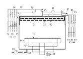
図1は、本発明の実施形態1の半導体デバイスの製造装置の模式的な構成図である。図1には、ウェハが収容されるカセット1と、カセット1から取り出されたウェハの位置決めを行うウェハアライメント2と、ロードロック機構を有するロードロックチャンバー3と、ウェハに絶縁物を形成するための第一チャンバー5と、第一チャンバー5において絶縁物が形成されたウェハに対して紫外光アニール処理を施す第二チャンバー6と、ロードロックチャンバー3,第一チャンバー5,第二チャンバー6相互間でウェハを搬送するロボットアームを有するトランスファーチャンバー4とを示している。
Hereinafter, embodiments of the present invention will be described with reference to the drawings. In addition, in each figure, the same code | symbol is attached | subjected to the same part.
(Embodiment 1)
FIG. 1 is a schematic configuration diagram of a semiconductor device manufacturing apparatus according to
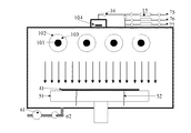
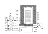
図2は、図1の第一チャンバー5の模式的な構成図である。図2には、SiN膜603(図4)を形成するためのアミノシラン(H3SiNH2)ガス、ジアミノシラン(H2Si(NH2)2)ガス、トリアミノシラン(HSi(NH2)3)ガス,テトラアミノシラン(Si(NH2)4)ガス、又はジメチルアミノシラン(H3SiN(CH3)2)ガス、ビス(ジメチルアミノ)シラン(H2Si(N(CH3)2)2)ガス、トリス(ジメチルアミノ)シラン(HSi(N(CH3)2)3)ガス、テトラキス(ジメチルアミノ)シラン(Si(N(CH3)2)4)ガス、ジシラン(Si2H6)ガスなどの供給管71と、トリアミノシランガス等の代替ガスであるところのテトラアミノジシラザン(H(NH2)2Si−NH−Si(NH2)2H)ガス又はテトラメチルジシラザン(H(CH3)2Si−NH−Si(CH3)2H)ガスの供給管72と、水蒸気の供給管73と、N2H4ガス等の供給管74と、ヘリウムガス、N2ガス等の供給管75とを示している。供給管71,72は、シリコン系ガスを第一チャンバー5に供給するためのものである。供給管74は、窒素系ガスを第一チャンバー5に供給するためのものである。供給管75は、不活性ガスを第一チャンバー5に供給するためのものである。なお、上記は、水素成分を含むシリコン系ガス系を使用する系で代表して説明したが、ハロゲン成分を含むシリコン系ガスを使用する場合は、供給管71又は72を通じて供給してもよく、新たに別の供給管を設置してもよい。
FIG. 2 is a schematic configuration diagram of the first chamber 5 of FIG. In FIG. 2, aminosilane (H 3 SiNH 2 ) gas, diaminosilane (H 2 Si (NH 2 ) 2 ) gas, triaminosilane (HSi (NH 2 ) 3 ) for forming the SiN film 603 (FIG. 4) are shown. gas, tetra aminosilane (Si (NH 2) 4) gas, or dimethylamino silane (H 3 SiN (CH 3) 2) gas, bis (dimethylamino) silane (H 2 Si (N (CH 3) 2) 2) gas , Tris (dimethylamino) silane (HSi (N (CH 3 ) 2 ) 3 ) gas, tetrakis (dimethylamino) silane (Si (N (CH 3 ) 2 ) 4 ) gas, disilane (Si 2 H 6 ) gas, etc.
各供給管71等は、それぞれ、バルブ16及びマスフローコントローラー15を介して、集合配管13に接続されている。集合配管13には、集合配管13を通る種々のガスを切り替えるためのバルブ14が取り付けられている。バルブ14の下流には、アルミナパイプ12が設けられている。
Each
また、第一チャンバー5内には、集合配管13を通るガスをウェハ41に対して噴霧するガスシャワーが設けられている。ガスシャワーは、当該ガスを第一チャンバー5に均一濃度で供給するためのガス分散板31と、ガス分散板31の下流に設けられていて複数の開口部33が形成されたシャワー板32が設けられている。
In the first chamber 5, a gas shower for spraying the gas passing through the collecting
また、図2には、第一チャンバー5をクリーニングするための三フッ化窒素(NF3)ガスの供給管81,酸素(O2)ガスの供給管82,及びアルゴン(Ar)ガスの供給管83と、SiN膜603を形成するためのNH3ガスの供給管84と、NH3ガスの代替ガスであるところのN2H4ガスの供給管85とを示している。供給管84、85は、窒素系ガスを第一チャンバー5に供給するためのものである。
FIG. 2 also shows a nitrogen trifluoride (NF 3 )
各供給管81等は、それぞれ、バルブ16及びマスフローコントローラー15を介して、各供給管81等を通る種々のガスを、第一チャンバー5に供給するのに先立ってプラズマ化するリモートプラズマ装置21に接続されている。リモートプラズマ装置21の近傍には、反応ガスのプラズマ化に必要な高周波を供給するRF発振器11が取り付けられている。
Each
また、第一チャンバー5には、ウェハ41を加熱する絶縁物(AlN又はAl)から成るヒーター51と、トランスファーチャンバー4によって搬送されてきたウェハ41を受けるリフトピン52と、リフトピン52を昇降させるための駆動機構53と、第一チャンバー5内のガスを排気する排気バルブ62と、排気バルブ62に接続されている排気ポンプ61とが接続されている。
The first chamber 5 includes a
図3は、図1の第二チャンバー6の模式的な構成図である。図3には、紫外光を照射する低圧水銀ランプ・Xeエキシマランプ及びメタルハライドランプなどの複数(例えば4つ)のランプ101と、減圧時にかかる応力から各ランプ101を保護するとともに各ランプ101への、酸素、シリコン系ガス、窒素系ガスの接触を防止する石英パイプ102と、石英パイプ102内に供給されるヘリウムガス、アルゴンガス、窒素ガス等の不活性ガス103と、連続的・定期的・間歇的にランプ101からの照射光の照度を測定する石英パイプ102内部或いは外部又は第二チャンバー6に取り付けられている受光センサー104とを示している。
FIG. 3 is a schematic configuration diagram of the second chamber 6 of FIG. FIG. 3 shows a plurality of (for example, four)
また、図3には、第二チャンバー6内に窒素ガスを供給するためのガス配管75と、ウェハ41を処理した後に第二チャンバー6内をクリーニングするための酸素ガス又はオゾンガスを供給するための供給管76と、同じく第二チャンバー6内で基板に吸着又は堆積したSi−H系、Si−NH系、SiO−NH系膜と反応させるためのN2H4ガス等の窒素系ガスを供給するための供給管77とを示している。なお、必要に応じて、窒素ガスに代わる不活性ガスを第二チャンバー6内に供給できるようにしてもよい。また、第一チャンバー5と第二チャンバー6とを兼用した、一つのチャンバーを用意してもよい。具体的には、第一チャンバー5内に、ランプ101等を設けることで実現できる。
FIG. 3 also shows a
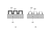
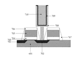
図4は、図1に示す半導体デバイス製造装置によって製造されるウェハ41の模式的な断面図である。図4(a)には、ゲート電極602が設けられているウェハ41上にSiN膜603が形成された状態を示している。図4(a)に示す状態から、SiN膜603を、図示しないエッチングチャンバーにおいて、既知の手法によって所要のエッチングをすれば、図4(b)に示すように、ゲート電極602に、サイドウォール604が形成されることになる。
FIG. 4 is a schematic cross-sectional view of a
つぎに、図1に示す半導体デバイスの製造装置による処理手順について説明する。本実施形態では、まず、図示しないクリーンルーム内の洗浄装置からフープ1に収容された状態で、ゲート電極602が設けられているウェハ41が搬送されてくる。その後、ウェハ41は、フープ1から取り出され、ウェハアライメント2側へ搬送される。
Next, a processing procedure performed by the semiconductor device manufacturing apparatus shown in FIG. 1 will be described. In the present embodiment, first, the
ウェハアライメント2では、ウェハ41の位置決めが行われる。その後、ウェハ41は、第一チャンバー5に搬送されるのに先立って、ロードロックチャンバー3に搬送される。
In the
つぎに、ロードロックチャンバー3内が減圧される。そして、ロードロックチャンバー3内が所望の圧力になると、ロードロックチャンバー3とトランスファーチャンバー4との間を仕切っているゲートバルブが開かれる。 Next, the pressure inside the load lock chamber 3 is reduced. When the pressure inside the load lock chamber 3 reaches a desired pressure, the gate valve that partitions the load lock chamber 3 and the transfer chamber 4 is opened.
その後、ウェハ41は、トランスファーチャンバー4内に搬送される。つづいて、トランスファーチャンバー4内のロボットアームによって、ロードロックチャンバー3内から第一チャンバー5内へ、ウェハ41が搬送されていく。
Thereafter, the
第一チャンバー5では、ヒーター51が、ウェハ41の表面温度が200℃〜450℃の範囲(例えば、300℃)となる条件で設定される。つぎに、固定式のヒーター51に対して、予め上方に位置するリフトピン52の上にウェハ41を載置させてから、駆動機構53によってリフトピン52を下降させて、ウェハ41をヒーター51上に載置させる。
In the first chamber 5, the
或いは、可動式のヒーター51を予め下降させておき、リフトピン52の上にウェハ41を載置させてから、ヒーター51を上昇させて、ウェハ41をヒーター51上に載置させてもよい。第一チャンバーでは、すでに排気ポンプ61がオンされ、かつ、排気バルブ62が開かれ、第一チャンバー5内は排気されている。
Alternatively, the
つづいて、供給管71に係るマスフローコントローラー15の制御によってバルブ16を開き、トリアミノシランガス等を50cc/min〜100cc/min(例えば75cc/min)の流量で、1分〜5分(例えば3分)間、第一チャンバー5に供給する。
Subsequently, the
この際、排気バルブ62は、第一チャンバー5内の圧力が133〜1330Pa(例えば399Pa)となる条件に開く。第一チャンバー5に供給されたトリアミノシランガス等は、ガス分散板31及びシャワー板32の開口部33を通じてウェハ41に到達する。
At this time, the
それから、第一チャンバー5内の圧力を13.3Pa〜133Pa(例えば67Pa)としてから、供給管71に係るバルブ16を閉じ、かつ、供給管74に係るバルブ16を開き、その後、N2H4ガスを400cc/min〜800cc/min(例えば600cc/min)の流量で流し、第一チャンバー5内の圧力を133Pa〜1330Pa(例えば399Pa)としてから、1分〜5分(例えば3分)間、第一チャンバー5にN2H4ガスを供給する。
Then, after the pressure in the first chamber 5 is set to 13.3 Pa to 133 Pa (for example, 67 Pa), the
その後、トリアミノシランガス等の供給からN2H4ガスの供給までのサイクルを、合計10回〜20回(例えば15回)繰り返す。この結果、ウェハ41のゲート電極602上には、30nm程度の厚さのSiN膜603が形成される。第一チャンバー5からウェハ41を取り出して、SiN膜603の屈折率を測定した。複数のウェハ41を対象として、SiN膜603の屈折率を測定したが、いずれもほぼ2.0以下であり、平均値は約1.95であった。また、ウェハ41のソース−ドレインの不純物プロファイルを計測すると、本実施形態では低温処理をしているため、チャネル領域に不純物が拡散しておらず、ソース−ドレインのショートは存在しなかった。
Thereafter, the cycle from the supply and triethylene amino silane gas to the supply of N 2 H 4 gas, a total of 10 times to 20 times (e.g. 15 times). As a result, an
なお、供給管71を通じたトリアミノシランガス等の供給に代えて、供給管72を通じたテトラアミノジシラザンガス等を、例えばトリアミノシランと同一流量、同一時間、供給してもよい。この場合にも、第一チャンバー5内の圧力を、テトラアミノジシラザンガス等とN2H4ガスとの供給時ともに、133Pa〜1330Pa(例えば399Pa)程度とすればよく、上記サイクル数を5回〜15回(例えば10回)とし、その他の条件は上記のとおりとしても、屈折率の平均が1.96程度で、30nm程度の厚さのSiN膜603が形成できる。
Instead of supplying the triaminosilane gas or the like through the
その後、ウェハ41に対して、第二チャンバー6において、254nm以上の波長を有する紫外光アニール処理を行う。紫外光アニール処理を行うと、消衰係数(吸収係数に相当するもの)が大きくなり、SiN膜603が緻密になるというメリットがある。紫外光アニール処理を行う場合には、ウェハ41は、トランスファーチャンバー4内のロボットアームによって、第一チャンバー5から第二チャンバー6に搬送される。
Thereafter, an ultraviolet light annealing process having a wavelength of 254 nm or more is performed on the
第二チャンバー6では、ウェハ41の表面温度が300〜450℃の範囲(例えば、400℃)となる条件でヒーター51が設定される。ここでは、第一チャンバー5のヒーター51より高い温度に設定してもよい。つぎに、ヒーター51の上に、ウェハ41が載置される。第二チャンバー6では、すでに排気ポンプ61がオンされ、かつ、排気バルブ62が開かれ、N2ガスを100cc/min〜300cc/min(例えば、200cc/min)を供給し、第二チャンバー6内の圧力が13.3Pa〜399Pa(例えば、133Pa)となる条件で排気されている。
In the second chamber 6, the
そして、ランプ101から、例えば、波長185+254nm、パワー10mW/cm2の低圧水銀光を、1分〜5分(例えば2分)照射することによって、ウェハ41の紫外線アニール処理を行う。
Then, place from the
また、第一チャンバー5は、10枚程度のウェハ41に対して既述の処理を行った後に、クリーニングされる。具体的には、マスフローコントローラー15の制御によってバルブ16を開き、ガス供給管81〜83を通じて、第一チャンバー5内に、約200cc/minの流量のArガスと、約100cc/minの流量のO2ガスと、約400cc/minの流量のNF3ガスとの混合ガスを、リモートプラズマ装置(又はRFプラズマ装置11)21に向けて出力する。
The first chamber 5 is cleaned after the above-described processing is performed on about ten
そして、リモートプラズマ装置21をオンして、各ガスをプラズマ化させて、チャンバー5に供給する。この際、排気ポンプ61をオンし、かつ、排気バルブ62を開くことで、第一チャンバー5内を排気する。排気時の第一チャンバー5内の圧力は、67〜399Pa程度とすればよい。
Then, the remote plasma device 21 is turned on to turn each gas into plasma and supply it to the chamber 5. At this time, the interior of the first chamber 5 is exhausted by turning on the
本実施形態では、屈折率の平均値が1.96程度で、30nm程度の厚さのSiN膜603が形成する場合を例に説明したが、3nm程度の厚さのSiN膜603を形成した半導体デバイスを製造することによって、シリコン酸化窒化酸化シリコン(SONOS)を組み込んだ、メモリ特性に優れた不揮発性メモリを実現することもできる。
In this embodiment, the case where the average value of the refractive index is about 1.96 and the
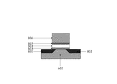
図5は、図1に示した装置を用いて製造した半導体デバイスを備える不揮発性メモリの模式的な一部断面図である。図5には、ウェハ41内に形成されたソース領域801及びドレイン領域802と、ウェハ41上に形成されたトンネル絶縁膜であるところのSiO2膜803と、SiN膜603上に形成されたフローティングゲート用のSiO2膜805と、SiO2膜805上に形成されたコントロールゲート806とを示している。
FIG. 5 is a schematic partial cross-sectional view of a non-volatile memory including a semiconductor device manufactured using the apparatus shown in FIG. FIG. 5 shows a
SiN膜603の形成は、既述のサイクル数を1回〜3回程度に減らすことによって実現できる。ただし、N2H4ガスの流量は同じで、トリアミノシランの流量を50cc/minと少なくしてもよい。
The formation of the
もっとも、この不揮発性メモリを製造する場合には、第一チャンバー5に搬送されるウェハ41は、すでに、ソース領域801及びドレイン領域802とSiO2膜803とが形成されている必要がある点には留意されたい。
However, when manufacturing this nonvolatile memory, the
また、20nm程度の厚さのSiN膜603を形成した半導体デバイスを製造することによって、小型のDRAMキャパシタを実現することもできる。
Also, a small DRAM capacitor can be realized by manufacturing a semiconductor device in which a
図6は、図1に示した製造装置を用いて製造した半導体デバイスを備えるDRAMキャパシタの模式的な一部断面図である。図6には、SiO2膜803上に選択的に形成されるHigh−k絶縁膜704と、High−k絶縁膜704上に形成されるメタル又はポリシリコン膜705と、メタル又はポリシリコン膜705上に形成されるSiO2膜706と、SiO2膜706の側壁に形成されるサイドウォールSiO2膜707と、ドレイン802上に形成されるキャパシタ下部電極(ポリシリコン)708と、キャパシタ下部電極に対してSiN膜603を介して形成されたキャパシタ上部電極710とを示している。
FIG. 6 is a schematic partial cross-sectional view of a DRAM capacitor including a semiconductor device manufactured using the manufacturing apparatus shown in FIG. FIG. 6 shows a high-
SiN膜603の形成は、既述のサイクル数を5〜10回程度に減らすことによって実現できる。
Formation of the
本実施形態では、ウェハ41上にSiN膜603を形成する場合を例に説明したが、第一チャンバー5に供給するガスを変更することによって、シリコン酸化膜(SiO2膜)又はシリコンオキシナイトライド膜(SiON膜)を形成することもできる。具体的には、SiO2膜を形成する場合には、供給管73を通じて水蒸気を、供給管75を通じてN2ガスを、それぞれ、100cc/min〜300cc/min(例えば、200cc/min)の流量で、同時に供給すればよい。
In this embodiment, the case where the
また、ウェハ41上にSiON膜を形成する場合には、N2H4ガスの供給時に、50cc/min〜100cc/min(例えば、75cc/min)の流量で、供給管73を通じて水蒸気を20cc/min〜100cc/min(例えば50cc/min)供給すればよい。なお、水蒸気を供給すると、デポレートが向上するため、既述のサイクル数は半分程度(5回〜10回)とすることができる。
In the case of forming the SiON film on the wafer 41, when the supply of
(実施形態2)
本発明の実施形態では、図1等に示した装置を用いて、実施形態1で説明したガスとは異なるガスを用いて、ウェハ41のゲート電極602上にSiN膜603を形成する方法について説明する。製造条件は、以下の点を除き、実施形態1の場合と同様である。
(Embodiment 2)
In the embodiment of the present invention, a method of forming the
1.トリアミノシランガス等に代えて、テトラアミノジシラザンガス等を用いる。したがって、供給管72に係るバルブ16を開くことになる。
1. Instead of triaminosilane gas or the like, tetraaminodisilazane gas or the like is used. Therefore, the
2.N2H4ガスに代えて、NH3ガスを用いる。したがって、供給管84に係るバルブ16を開くことになる。NH3ガスの流量は、400cc/min〜800cc/min(例えば600cc/min)とする。
2. NH 3 gas is used instead of N 2 H 4 gas. Therefore, the
3.供給管84に係るバルブ16を開いた後、リモートプラズマ装置21を、1分〜5分(例えば3分)間、オンする。リモートプラズマ装置21は、例えば、13.56MHz又は400Hzの高周波を用い、400W〜1000W(例えば750W)の出力で、NH3ガスをプラズマ化する。この結果、NH3ガスは、プラズマ化された状態で、第一チャンバー5に供給される。
3. After opening the
なお、上記各ガスを数回に亘り第一チャンバー5に供給するだけではなく、また、テトラアミノジシラザンガスとNH3ガスとを交互だけではなく、1回のみ一緒に、20秒間〜50秒間(例えば30秒間)供給することも可能である。この際、ガスの「流量」、「圧力」、「温度」については、上記1〜3の場合と同様としてよい。
In addition to supplying each gas to the first chamber 5 several times, the tetraaminodisilazane gas and the NH 3 gas are not only alternated, but only once together for 20 seconds to 50 seconds. It is also possible to supply (for example 30 seconds). At this time, the “flow rate”, “pressure”, and “temperature” of the gas may be the same as those in the
この結果、ウェハ41には、屈折率の平均値が1.97程度で、厚さが約50nmのSiN膜603が形成できる。
As a result, an
本実施形態のウェハ41についても、実施形態1の場合と同様に、SiN膜603の厚さを適宜選択することによって、不揮発性メモリ、DRAMキャパシタなどに組み込むことが可能となる。以下説明する各実施形態においても同様である。
Similarly to the case of the first embodiment, the
(実施形態3)
本発明の実施形態では、図1等に示した製造装置を用いて、実施形態1で説明したガスとは異なるガスを用いて、ガラス基板上にSiN膜603を形成する。製造条件は、以下の点を除き、実施形態1の場合と同様である。
(Embodiment 3)
In the embodiment of the present invention, the
1.ウェハ41をガラス基板とする。
1. The
2.N2H4ガスに代えて、NH3ガスを用いる。なお、NH3ガスの流量、プラズマ化の条件は、実施形態2と同じでよい。 2. NH 3 gas is used instead of N 2 H 4 gas. The flow rate of NH 3 gas and the conditions for plasma formation may be the same as those in the second embodiment.
3.上記各ガスを数回に亘り第一チャンバー5に供給するだけ(この場合には実施形態2と同じ条件)ではなく、また、トリアミノシランガス等とNH3ガスとを交互だけではなく、1回のみ一緒に、1分間〜3分(例えば2分)間供給してもよい。 3. Each of the above gases is not only supplied to the first chamber 5 several times (in this case, the same conditions as in the second embodiment), and triaminosilane gas or the like and NH 3 gas are not only alternately but once. Only together, it may be supplied for 1 to 3 minutes (for example, 2 minutes).
4.上記各ガスの供給時には、第一チャンバー5内の圧力は、13.3Pa〜1330Pa(例えば399Pa)とする。 4). When supplying each gas, the pressure in the first chamber 5 is 13.3 Pa to 1330 Pa (for example, 399 Pa).
この結果、ウェハ41には、屈折率の平均値が1.93程度で、厚さが約100nmのSiN膜603が形成できる。
As a result, an
その後、ウェハ41は、例えば実施形態1と同じ条件で、200〜400℃(300℃)で紫外光アニール処理を行う。ガラス基板ウェハ41上にN型のアモーファスシリコンを約100nmの厚さで形成し、その上に本実施形態の手法によってSiN膜を約100nm形成した。そして、SiN膜の紫外線アニール処理を行った。さらに、SiN膜の上にSiO2膜を約100nmの厚さで形成した。そしてさらにその上にN型のアモーファスシリコンを100nm形成し、パターニングし、上下のアモーファスシリコンに電圧200Vと温度300℃とをかけた後、C−V測定によりVFBシフトを調べたところ、ガラス基板ウェハ41からナトリウム等が拡散している事実は認められなかった。
Thereafter, the
なお、トリアミノシランガス等に代えて、テトラアミノジシラザンガス等を用いてもよい。この際、SiN膜603の形成に要する時間の短縮が必要ないのであれば、まず、テトラアミノジシラザンガス等を、50cc/min〜100cc/min(例えば75cc/min)の流量で、1分〜5分(例えば3分)間、133〜1330Pa(例えば399Pa)の条件で第一チャンバー5に供給する。
Instead of triaminosilane gas or the like, tetraaminodisilazane gas or the like may be used. At this time, if it is not necessary to shorten the time required for forming the
また、同様にNH3ガスを用い、プラズマ化したNH3ガスを、400cc/min〜800cc/min(例えば600cc/min)の流量で、1分〜5分(例えば2分)間、13.3Pa〜1330Pa(例えば399Pa)程度の条件で、第一チャンバー5に供給する。この場合、テトラアミノジシラザンガス等の供給と、NH3ガスの供給とを交互に、合計15回〜25回(例えば20回)のサイクルで繰り返せばよい。 Similarly, NH 3 gas is used, and plasmaized NH 3 gas is supplied at a flow rate of 400 cc / min to 800 cc / min (eg, 600 cc / min) for 1 minute to 5 minutes (eg, 2 minutes), 13.3 Pa. It supplies to the 1st chamber 5 on about 1330 Pa (for example, 399 Pa) conditions. In this case, the supply of tetraaminodisilazane gas or the like and the supply of NH 3 gas may be alternately repeated in a total of 15 to 25 times (for example, 20 times).
なお、テトラアミノジシラザンガス等を用いる場合にも、テトラアミノジシラザンガスとN2H4ガスとを同時に供給するときには、各ガスの供給時間を15秒間〜40秒間(例えば25秒間)と短縮しただけで、他の条件は本実施形態のとおりとしても、ウェハ41には、屈折率の平均値が1.97程度で、厚さが約100nmのSiN膜603が形成できる。
Even when tetraaminodisilazane gas or the like is used, when supplying tetraaminodisilazane gas and N 2 H 4 gas at the same time, the supply time of each gas is reduced to 15 seconds to 40 seconds (for example, 25 seconds). However, even if other conditions are the same as in this embodiment, the
(実施形態4)
本発明の実施形態では、図1等に示した製造装置を用いて、実施形態1で説明した手法とは異なる手法で、ウェハ41のゲート電極602上にSiN膜603を形成する方法について説明する。製造条件は、以下の点を除き、実施形態1の場合と同様である。
(Embodiment 4)
In the embodiment of the present invention, a method of forming the
1.トリアミノシランガス等とプラズマによって励起されたNH3ガスを交互に供給することによりSiN膜603を形成する。具体的には、ウェハ41のゲート電極602上に、Si−NH膜が約2nmの厚さで形成される。流量及び圧力は実施形態3と同様の条件である。
1. The
2.実施形態2と同様の条件でリモートプラズマ装置21によってプラズマ化したNH3ガスを、圧力が67Pa〜399Pa(例えば、133Pa)とされた第一チャンバー5に供給する。NH3ガスは、流量を400cc/min〜800cc/min(例えば600cc/min)とし、かつ、供給時間を1分〜5分(例えば3分)間とすればよい。 2. NH 3 gas that has been converted to plasma by the remote plasma apparatus 21 under the same conditions as in the second embodiment is supplied to the first chamber 5 having a pressure of 67 Pa to 399 Pa (eg, 133 Pa). NH 3 gas flow rate and the 400cc / min~800cc / min (e.g. 600cc / min), and the supply time may be set to between 1 to 5 minutes (e.g. three minutes).
この結果、先に形成したSi−NH膜が窒化され、厚さが約20nmで、屈折率の平均値が1.99のSiN膜603が得られる。
As a result, the previously formed Si—NH film is nitrided, and an
なお、またSiN膜603を形成した後、低圧水銀以上の波長を有する紫外線を照射してSiN膜603をさらに強固にしてもよい。
In addition, after forming the
(実施形態5)
本発明の実施形態では、図1等に示した製造装置を用いて、実施形態1で説明した手法とは異なる手法で、ウェハ41のゲート電極602上にSiN膜603を形成する方法について説明する。製造条件は、以下の点を除き、実施形態1の場合と同様である。
(Embodiment 5)
In the embodiment of the present invention, a method of forming the
1.トリアミノシランガス等と照度を10W/cm2程度とした紫外光照射によって励起されたNH3ガスを交互に供給することによりSi−NH膜を形成する。具体的には、ウェハ41のゲート電極602上に、Si−NH膜が約2nmの厚さで形成される。各ガスの流量及び圧力は実施形態3と同様の条件である。
1. A Si-NH film is formed by alternately supplying triaminosilane gas or the like and NH 3 gas excited by ultraviolet light irradiation with an illuminance of about 10 W / cm 2 . Specifically, a Si—NH film is formed with a thickness of about 2 nm on the
2.紫外光照射によって励起されたNH3ガスを、圧力が67Pa〜399Pa(例えば、133Pa)とされた第一チャンバー5に供給する。NH3ガスは、流量を400cc/min〜800cc/min(例えば600cc/min)とし、かつ、供給時間を1分〜5分(例えば3分)間とすればよい。 2. NH 3 gas excited by ultraviolet light irradiation is supplied to the first chamber 5 having a pressure of 67 Pa to 399 Pa (eg, 133 Pa). NH 3 gas may have a flow rate of 400 cc / min to 800 cc / min (eg, 600 cc / min) and a supply time of 1 minute to 5 minutes (eg, 3 minutes).
この結果、紫外光によって励起されたNH3ガスと同時に紫外光により膜中の結合基が励起又は分解されたSi−NH膜がより効率的に反応し、厚さが約20nmで、屈折率の平均値が1.99のSiN膜603が得られる。
As a result, the Si—NH film in which the bonding group in the film is excited or decomposed by the ultraviolet light simultaneously with the NH 3 gas excited by the ultraviolet light reacts more efficiently, has a thickness of about 20 nm, and has a refractive index of A
なお、450℃以下の加温によって、N2H4ガスを分解してもよい。またまたSiN膜603を形成した後、低圧水銀光以上の波長を有する紫外光を照射してSiN膜603をさらに強固にしてもよい。
Incidentally, the following heating 450 ° C., may decompose
(実施形態6)
本発明の実施形態では、図1等に示した製造装置を用いて、実施形態1で説明した手法とは異なる手法で、ウェハ41のゲート電極602上にSiN膜603を形成する方法について説明する。製造条件は、以下の点を除き、実施形態1の場合と同様である。
(Embodiment 6)
In the embodiment of the present invention, a method of forming the
1.トリアミノシランガスに代えてジシランガス等と、照度を10W/cm2程度とした紫外光照射によって励起されたNH3ガスとを交互に供給することによりSiN膜603を形成する。具体的には、ウェハ41のゲート電極602上に、Si−H膜が約2nmの厚さで形成される。各ガスの流量及び圧力は実施形態4と同様の条件である。
1. A
2.紫外光照射装置によって分解したNH3ガスを、圧力が67Pa〜399Pa(例えば、133Pa)とされた第一チャンバー5に供給する。NH3ガスは、流量を400cc/min〜800cc/min(例えば600cc/min)とし、かつ、供給時間を1分〜5分(例えば3分)間とすればよい。 2. NH 3 gas decomposed by the ultraviolet light irradiation device is supplied to the first chamber 5 having a pressure of 67 Pa to 399 Pa (eg, 133 Pa). NH 3 gas may have a flow rate of 400 cc / min to 800 cc / min (eg, 600 cc / min) and a supply time of 1 minute to 5 minutes (eg, 3 minutes).
この結果、先に形成したSi−H膜が窒化され、厚さが約20nmで、屈折率の平均値が2.0のSiN膜603が得られる。
As a result, the previously formed Si—H film is nitrided, and a
なお、450℃以下の加温によって、N2H4ガスを分解してもよい。またまたSiN膜603を形成した後、低圧水銀光以上の波長を有する紫外光を照射してSiN膜603をさらに強固にしてもよい。
Note that the N 2 H 4 gas may be decomposed by heating at 450 ° C. or lower. Further, after forming the
(実施形態7)
図7は、本発明の実施形態7に係る第一チャンバー5の模式的な構成図である。図7に示す第一チャンバー5は、端的に言えば、リモートプラズマ装置21の配置を変更した点と、内部にランプ101を設けている点と、複数の開口を有する石英板111と石英板112とを設けている点とが、図2に示したものとは相違する。
(Embodiment 7)
FIG. 7 is a schematic configuration diagram of the first chamber 5 according to Embodiment 7 of the present invention. Briefly speaking, the first chamber 5 shown in FIG. 7 includes a point where the arrangement of the remote plasma apparatus 21 is changed, a point where a
図7に示す第一チャンバー5を用いた半導体ウェハの製造方法について説明する。 A method for manufacturing a semiconductor wafer using the first chamber 5 shown in FIG. 7 will be described.
まず、ヒーター51の温度は、ランプ101を用いているため実施形態1の場合に比して低くしてよい。具体的には、200℃〜400℃の範囲(例えば、300℃)程度でよい。また、ランプ101は、172nm波長の光を照射可能なXeエキシマランプを用い、照度は10mW/cm2程度とすればよい。
First, since the
第一チャンバー5に対する供給ガスは、テトラキス(ジメチルアミノ)シランガス等とNH3ガス又はN2H4ガスとすることができる。各ガスの流量は、それぞれ、50cc/min〜100cc/min(例えば75cc/min)、400cc/min〜800cc/min(例えば600cc/min)程度とすればよい。 The supply gas to the first chamber 5 can be tetrakis (dimethylamino) silane gas or the like and NH 3 gas or N 2 H 4 gas. The flow rate of each gas may be about 50 cc / min to 100 cc / min (for example, 75 cc / min) and about 400 cc / min to 800 cc / min (for example, 600 cc / min), respectively.
また、NH3ガス又はN2H4ガスに加えて、紫外光ランプを保護する石英管102に生成物が付着しないためにN2ガスを追加してもよい。N2ガスは、200cc/min〜600cc/min(例えば400cc/min)程度とすればよい。ガス供給バルブ16を開き、NH3ガス又はN2H4ガスとN2ガスとをチャンバー5に供給する。その後、テトラキス(ジメチルアミノ)シランガスを石英板111と石英板112との間に供給する。
In addition to NH 3 gas or N 2 H 4 gas, N 2 gas may be added so that the product does not adhere to the
また、各ガスの供給時間は、30秒間から90秒間(例えば60秒間)とし、第一チャンバー5内の圧力は、13.3Pa〜399Pa(例えば67Pa)とする。そして、NH3ガス又はN2H4ガスが流れている間、Xeエキシマランプを点灯させる。この結果、厚さが20nmで屈折率の平均が2.0のSiN膜603がウェハ41上に形成される。
The supply time of each gas is 30 seconds to 90 seconds (for example, 60 seconds), and the pressure in the first chamber 5 is 13.3 Pa to 399 Pa (for example, 67 Pa). Then, the Xe excimer lamp is turned on while NH 3 gas or N 2 H 4 gas is flowing. As a result, a
ここでは、DRAMキャパシタ用の半導体ウェハに好適な製造条件を例示したが、半導体ウェハの組み込み対象に応じて、例えばガスの供給方法及び時間を変更すれば、種々の電子機器に適用することができる。 Here, manufacturing conditions suitable for semiconductor wafers for DRAM capacitors have been illustrated, but can be applied to various electronic devices if, for example, the gas supply method and time are changed according to the target of incorporation of the semiconductor wafer. .
一例をあげると、図7に示す第一チャンバー5を用いて不揮発性メモリを製造する場合には、ヒーター51の温度をウェハ41の表面温度が150℃〜450℃の範囲(例えば、300℃)程度となる条件で設定する。また、テトラキス(ジメチルアミノ)シランガス等の流量は、20cc/min〜100cc/min(例えば50cc/min)とし、N2H4ガスの流量は、200cc/min〜800cc/min(例えば400cc/min)とする。
For example, in the case of manufacturing a non-volatile memory using the first chamber 5 shown in FIG. 7, the temperature of the
XeエキシマランプはNH3ガス又はN2H4ガスが流れている間点灯させる。テトラキス(ジメチルアミノ)シランガス等とN2H4ガス等は交互に供給し、各ガスの供給時間は、20秒間から60秒間(例えば30秒間)とする。各ガスを供給した後には、チャンバーの圧力を1.33Pa〜133Paと低くする。各ガスが供給されている間は、第一チャンバー5内の圧力は、13.3〜399Pa(例えば67Pa)とする。各ガスのパルスサイクルを2回繰り返せば、厚さが3nmで屈折率の平均値が1.97のSiN膜603がウェハ41上に形成される。
Xe excimer lamp is turned between the NH 3 gas or N 2 H 4 gas is flowing. Tetrakis (dimethylamino) silane gas or the like and N 2 H 4 gas or the like are supplied alternately, and the supply time of each gas is 20 seconds to 60 seconds (for example, 30 seconds). After supplying each gas, the pressure of the chamber is lowered to 1.33 Pa to 133 Pa. While each gas is supplied, the pressure in the first chamber 5 is set to 13.3 to 399 Pa (for example, 67 Pa). If the pulse cycle of each gas is repeated twice, a
或いは、厚さが20nmで屈折率が1.97のSiN膜603をウェハ41上に形成するためには、まず、例えば、N2ガスを100cc/min〜500cc/min(例えば200cc/min)の流量でチャンバー5に供給する。つぎに、第一チャンバー5内の圧力を13.3〜133Pa(例えば67Pa)程度にして、N2H4ガスを200cc/min〜800cc/min(例えば400cc/min)の流量で連続供給する。N2H4ガスが供給されている間、Xeエキシマランプを点灯させる。
Alternatively, in order to form the
テトラキス(ジメチルアミノ)シランガス又はトリス(ジメチルアミノ)シランガスを、図7に示す第一チャンバー5内に設置してある、仕切り板であるところの穴の開いた石英板111と石英板112とで囲まれている領域に20cc/min〜100cc/min(例えば50cc/min)の流量で10秒〜30秒(例えば20秒)間、供給する。この操作を1回〜10回繰り返す(例えば5回)。この際、第一チャンバー5内の圧力は、13.3Pa〜399Pa(例えば67Pa)とする。 Tetrakis (dimethylamino) silane gas or tris (dimethylamino) silane gas is surrounded by the quartz plate 111 and the quartz plate 112 which are installed in the first chamber 5 shown in FIG. The region is supplied at a flow rate of 20 cc / min to 100 cc / min (for example, 50 cc / min) for 10 to 30 seconds (for example, 20 seconds). This operation is repeated 1 to 10 times (for example, 5 times). At this time, the pressure in the first chamber 5 is set to 13.3 Pa to 399 Pa (for example, 67 Pa).
そして、テトラキス(ジメチルアミノ)シランガス又はトリス(ジメチルアミノ)シランガスが供給されている間、また、ランプ101は、172nm波長の光を照射可能なXeエキシマランプを用い、照度は10mW/cm2程度とすればよい。このようにして、厚さが約20nmのSiN膜603が得られる。
While the tetrakis (dimethylamino) silane gas or the tris (dimethylamino) silane gas is being supplied, the
また下部の石英板102の穴を大きくし、また除去して、石英坂102に生成物の付着をなくすようにして、172nm波長の光を照射可能なXeエキシマランプを連続照射しても良い。この場合には254nm波長の光を連続照射可能な低圧Hgランプを用いても良い。
Alternatively, the hole in the
(実施形態8)
図8は、本発明の実施形態8に係る減圧CVD装置の模式的な構成図である。図8に示す減圧CVD装置は、実施形態7までに説明したいわゆるクラスタタイプのチャンバーではなく、バッチタイプのチャンバーである。この種のチャンバーを用いると、1回の処理で複数のウェハ41にSiN膜603を形成することができるという利点がある。
(Embodiment 8)
FIG. 8 is a schematic configuration diagram of a low pressure CVD apparatus according to Embodiment 8 of the present invention. The low-pressure CVD apparatus shown in FIG. 8 is not a so-called cluster type chamber described in the seventh embodiment but a batch type chamber. When this type of chamber is used, there is an advantage that the
図8には、Heガスの供給管200と、水蒸気の供給管201と、NH3ガスの供給管202、N2H4ガスの供給管203と、トリアミノシラン(H−Si(NH2)3)ガスの供給管204と、トリアミノシランガスの代替ガスであるトリス(ジメチルアミノ)シラン(H−Si(N(CH3)2)3ガス、又はテトラキス(ジメチルアミノ)シランガスの供給管205と、トリアミノシランガスの代替ガスであるテトラアミノジシラザン((H(NH2)Si−NH−Si((NH2)H)ガスの供給管206と、トリアミノシランガスの代替ガスであるテトラメチルアミノジシラザン((HN(CH3)2)Si−N−Si((N(CH3)2H)ガスの供給管207と、N2ガスの供給管208とを示している。すなわち、供給管200は、不活性ガス供給管であり、供給管202は、窒素系ガス供給管であり、供給管203〜207はシリコン系ガス供給管であり、供給管208は、不活性ガス供給管である。
8 includes a
また、図8には、各供給管200〜208に接続されているエアーバルブ209と、種々のガスの流量を制御するマスフローコントローラー210と、種々のガスが通る複数穴が形成されている内部石英管213と、内部石英管213の周辺を覆っていて減圧CVD処理室を形成する外部石英管212と、各石英管212,213を加熱するヒーター211と、複数のウェハ41を把持するウェハホルダー214と、ウェハホルダー214が載置される石英バッファー216とを示している。
FIG. 8 also shows an
さらに、図8には、種々のガスをウェハ41に向けて噴射するノズル317と、ノズル317に形成されているノズル孔318と、各供給管200〜208をまとめるマニホールド321と、内部石英管213及び外部石英管212が載置される石英管台222と、外部石英管212に連結されている排気バルブ231と、排気バルブ231の近傍に設けられた圧力計232と、圧力計232の計測結果に従って排気バルブ231を調整する圧力調整バルブ233と、外部石英管212及び内部石英管213内を排気する排気ポンプ234と、ウェハ41をウェハホルダー214に搬送するウェハ搬送ロボット241と、N2ガスを充満したシールドボックス242とを示している。
Further, FIG. 8 shows a
図8に示す減圧CVD装置でのウェハ41の処理自体は、既知の手法と同様であるが、ヒーター211でウェハ41の表面温度が300℃〜450℃(例えば400℃)となる条件に設定し、N2ガスを供給し、内部石英管213内の圧力を67Pa〜399Pa(例えば、133Pa)とした状態で、ゲート電極602の形成されたウェハ41が把持されたウェハホルダー214が収容された減圧CVD装置に対して、10分〜30分(例えば20分)間程度、以下の条件でガスを供給する。
The processing itself of the
1.アミノシランガスを100cc/min〜300cc/min(例えば200cc/min)程度の流量で供給する。 1. Aminosilane gas is supplied at a flow rate of about 100 cc / min to 300 cc / min (for example, 200 cc / min).
2.供給管203を通じてN2H4ガスを400cc/min〜1000cc/min(例えば800cc/min)程度の流量で供給する。
2. N 2 H 4 gas is supplied through the
3.供給管201を通じてノズル317から水蒸気を30cc/min〜70cc/min(例えば50cc/min)程度の流量で供給する。水蒸気の供給は、アミノシランガスの分解を促進する。
3. Water vapor is supplied from the
4.供給管200を通じてHeガスを100cc/min〜500cc/min(例えば300cc/min)程度の流量で供給する。
4). He gas is supplied through the
この結果、厚さが50nmで、屈折率が1.85のSiON膜が得られる。 As a result, a SiON film having a thickness of 50 nm and a refractive index of 1.85 is obtained.
なお、アミノシランガスのみならず、代えて、テトラキス(ジメチルアミノ)シランガス、テトラアミノジシラザンガス、テトラメチルアミノジシラザンガス、更には、図2等を用いて説明したトリス(ジメチルアミノ)シランガス等を用いてもよい。なお、ガスの供給時間は、使用ガスに応じて決定すればよい。 Instead of aminosilane gas, instead of tetrakis (dimethylamino) silane gas, tetraaminodisilazane gas, tetramethylaminodisilazane gas, and tris (dimethylamino) silane gas described with reference to FIG. It may be used. Note that the gas supply time may be determined according to the gas used.
(実施形態9)
図8等に示した装置を用いて、実施形態8で説明したガスとは異なるガスを用いて、ウェハ41のゲート電極602上にSiN膜603を形成する方法について説明する。製造条件は、以下の点を除き、実施形態6の場合と同様である。
(Embodiment 9)
A method of forming the
1.減圧CVD装置内に、2種類のガスを交互に供給する。なお、内部石英管213内のウェハ41の表面温度が、200℃〜450℃(例えば300℃)となるように設定する。
1. Two kinds of gases are alternately supplied into the low pressure CVD apparatus. The surface temperature of the
2.内部石英管213内の圧力を133Pa〜1330Pa(例えば、399Pa)として、テトラキス(ジメチルアミノ)シランガスを100cc/min〜300cc/min(例えば200cc/min)の流量で1分〜5分(例えば3分)間程度供給する。
2. The pressure in the
3.つぎに、テトラキス(ジメチルアミノ)シランガスの供給を止め、内部石英管213内の圧力を、1.33Pa〜133Pa(例えば67Pa)としてから、ノズル317からN2H4ガスを400cc/min〜1000cc/min(例えば800cc/min)の流量で、内部石英管213内の圧力を、再度、133Pa〜1330Pa(例えば、399Pa)として、1分〜5分(例えば3分)間程度供給する。
3. Next, the supply of the tetrakis (dimethylamino) silane gas is stopped, the pressure in the
上記各ガスの供給を交互に、合計10回〜20回(例えば15回)のサイクルで繰り返す。 The supply of each gas is alternately repeated in a total of 10 to 20 (for example, 15) cycles.
この結果、厚さが30nmで、屈折率の平均値が1.95のSiN膜603が得られる。
As a result, a
なお、N2H4ガスに代えて、NH3ガスを用い、かつ、NH3ガスをリモートプラズマ装置で励起した状態で供給すれば、サイクル数は、2/3程度に減らすことができる。 Note that if NH 3 gas is used instead of N 2 H 4 gas and NH 3 gas is supplied in a state excited by a remote plasma apparatus, the number of cycles can be reduced to about 2/3.
(実施形態10)
図8等に示した装置を用いて、実施形態8で説明したガスとは異なるガスを用いて、ウェハ41のゲート電極602上にSiN膜603を形成する方法について説明する。製造条件は、以下の点を除き、実施形態6の場合と同様である。
(Embodiment 10)
A method of forming the
具体的には、図8の供給管205を、トリス(ジメチルアミノ)シラン(H−Si(N(CH3)2)3ガス、ジシラン(Si2H6)ガスの供給管に変更した。 Specifically, the supply pipe 205 in FIG. 8 was changed to a supply pipe for tris (dimethylamino) silane (H—Si (N (CH 3 ) 2 ) 3 gas and disilane (Si 2 H 6 ) gas.
図8に示す減圧CVD装置でのウェハ41の処理自体は、既知の手法と同様であるが、ヒーター211でウェハ41の表面温度を300℃〜450℃(例えば400℃)に加熱し、N2ガスを供給し、内部石英管213内の圧力を67Pa〜399Pa(例えば、133Pa)とした状態で、ゲート電極602の形成されたウェハ41が把持されたウェハホルダー214が収容された減圧CVD装置に対して、10分〜30分(例えば、20分)間程度、以下の条件でガスを供給する。
The processing itself of the
1.ノズル317からジシランガスを100cc/min〜300cc/min(例えば200cc/min)程度の流量で供給する。
1. Disilane gas is supplied from the
2.ジシランガスの供給と同時に、供給管203を通じてN2H4ガスを400cc/min〜1000cc/min(例えば800cc/min)程度の流量で供給する。
2. Simultaneously with the supply of disilane gas, supplying the N 2 H 4 gas in 400cc / min~1000cc / min (e.g. 800 cc / min) flow rate of about through the
3.供給管200を通じてHeガスを100cc/min〜600cc/min(例えば300cc/min)程度の流量で供給する。
3. He gas is supplied through the
この結果、厚さが50nmで、屈折率が1.97のSiN膜603が得られる。
As a result, a
(実施形態11)
図8等に示した装置を用いて、実施形態8で説明したガスとは異なるガスを用いて、ウェハ41のゲート電極602上にSiN膜603を形成する方法について説明する。製造条件は、以下の点を除き、実施形態6の場合と同様である。
(Embodiment 11)
A method of forming the
具体的には、図8の供給管205を、トリスジメチルアミノシラン(H−Si(N(CH3)2)3ガス、ジシラン(Si2H6)ガスの供給管に変更した。 Specifically, the supply pipe 205 in FIG. 8 was changed to a supply pipe for trisdimethylaminosilane (H—Si (N (CH 3 ) 2 ) 3 gas and disilane (Si 2 H 6 ) gas.
図8に示す減圧CVD装置でのウェハ41の処理自体は、既知の手法と同様であるが、ヒーター211でウェハ41の表面温度を300℃〜450℃(例えば400℃)に加熱し、内部石英管213内にジシランガスとヒドラジンガスを交互に供給することが異なる。ゲート電極602の形成されたウェハ41が把持されたウェハホルダー214が収容された減圧CVD装置に対して、1分〜5分(例えば3分)間程度、以下の条件でガスを供給する。
The processing itself of the
1.ノズル317からジシランガスを100cc/min〜300cc/min(例えば200cc/min)程度の流量で供給する。圧力は133Pa〜1330Pa(例えば399Pa)で1分〜5分(例えば3分)間供給する。その後、圧力を1.33Pa〜133Pa(例えば67Pa)に減圧する。
1. Disilane gas is supplied from the
2.つぎに、供給管203を通じてN2H4ガスを400cc/min〜1000cc/min(例えば800cc/min)程度の流量で1分〜5分(例えば3分)間供給する。圧力は、133Pa〜1330Pa(例えば399Pa)にする。また、N2H4ガスとともに、供給管200を通じてHeガスを100cc/min〜500cc/min(例えば300cc/min)程度の流量で供給してもよい。その後、圧力を1.33Pa〜133Pa(例えば67Pa)に減圧する。
2. Then, N 2 H 4 gas 400cc / min~1000cc / min (e.g. 800 cc / min) 1 to 5 minutes at a flow rate of about (for example, 3 minutes) for supplying through the
3.この操作を1回から10回まで(例えば2回)繰り返す。 3. This operation is repeated from 1 to 10 times (for example, twice).
この結果、厚さが3nmで、屈折率が2.0のSiN膜603が得られる。
As a result, a
(実施形態12)
図7に示した第一チャンバー5を用いて、実施形態7で説明した方法とは異なる方法を用いて、ウェハ41のゲート電極上にSiN膜を形成する方法について説明する。製造条件は、以下の点を除き、実施形態7の場合と同様である。
A method of forming a SiN film on the gate electrode of the
1.ヒーター51の温度を、ウェハ41の表面温度がシリコン系ガスの沸点(常圧下のもの)以下の温度となる条件に設定する。
1. The temperature of the
2.第一チャンバー5内の圧力を133Pa〜1330Pa(例えば、399Pa)、ヒーター51の温度をウェハ41の表面温度が50℃〜180℃(例えば140℃)となる条件に設定して、テトラキス(ジメチルアミノ)シランガスを100cc/min〜300cc/min(例えば200cc/min)の流量で1分〜5分(例えば3分)間程度供給する。
2. The pressure in the first chamber 5 is set to 133 Pa to 1330 Pa (for example, 399 Pa), the temperature of the
3.つぎに、テトラキス(ジメチルアミノ)シランガスの供給を止め、第一チャンバー5内の圧力を、1.33Pa〜133Pa(例えば67Pa)としてから、N2H4ガスを400cc/min〜1000cc/min(例えば800cc/min)の流量で、第一チャンバー5内の圧力を、再度、133Pa〜1330Pa(例えば、399Pa)として1分〜5分(例えば3分)間程度供給する。この際、実施形態7と同様に、ランプ101から紫外線を照射する。ただし、「温度」は、50℃〜180℃(例えば140℃)のままである。
3. Next, the supply of tetrakis (dimethylamino) silane gas is stopped and the pressure in the first chamber 5 is set to 1.33 Pa to 133 Pa (for example, 67 Pa), and then N 2 H 4 gas is supplied from 400 cc / min to 1000 cc / min (for example, At a flow rate of 800 cc / min), the pressure in the first chamber 5 is again supplied as 133 Pa to 1330 Pa (for example, 399 Pa) for about 1 minute to 5 minutes (for example, 3 minutes). At this time, similarly to the seventh embodiment, the
上記各ガスの供給を交互に、合計5回〜10回(例えば7回)のサイクルで繰り返す。 The supply of each gas is alternately repeated in a total of 5 to 10 (for example, 7) cycles.
この結果、厚さが30nmで、屈折率の平均値が1.93のSiN膜が得られる。 As a result, a SiN film having a thickness of 30 nm and an average refractive index of 1.93 is obtained.
なお、N2H4ガスに代えて、NH3ガスを用い、かつ、NH3ガスをリモートプラズマ装置で励起した状態で供給してもよい。 Note that NH 3 gas may be used instead of N 2 H 4 gas, and NH 3 gas may be supplied in a state excited by a remote plasma apparatus.
また、本実施形態では相対的に低温でSiN膜を形成しているため、その後、第一チャンバー5内のウェハ41の表面温度が450℃以下となる条件で加熱してアニール処理を行い、あるいは、別な炉等にSiN形成後のウェハ41を搬送して、そこで450℃以下に加熱した状態でアニール処理を行うと、SiN膜が緻密になる。
In addition, since the SiN film is formed at a relatively low temperature in the present embodiment, after that, annealing is performed by heating under the condition that the surface temperature of the
以上、本発明の各実施形態について説明したが、ここで、各実施形態の内容の概要についてまとめておく。 As mentioned above, although each embodiment of this invention was described, here, the outline | summary of the content of each embodiment is put together.
表1は、実施形態1〜12における、半導体デバイスの製造装置の種別、半導体デバイスの製造方法の方式、使用ガス等をまとめた表である。なお、使用ガスは(1)シリコン系ガス、(2)窒素系ガス(3)選択的に用いるガスとしている。
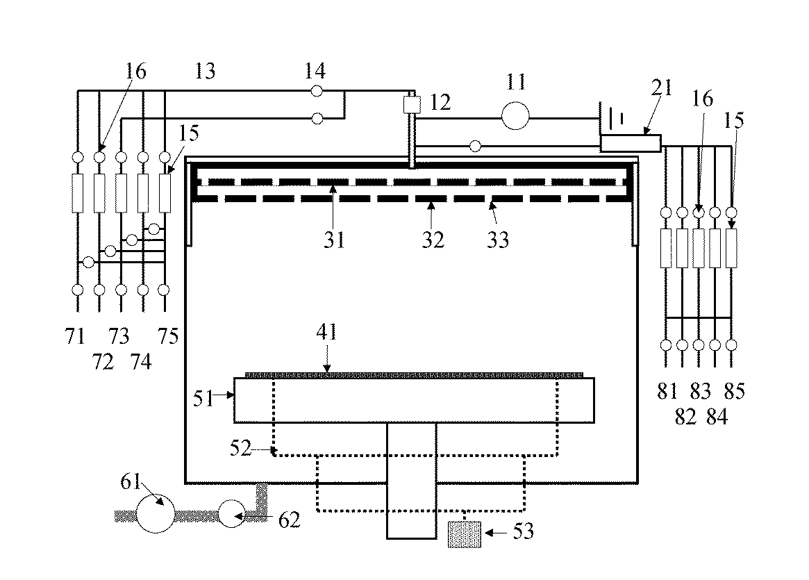
表2,表3は、実施形態1〜12における、使用ガス、ガスの流量、チャンバー等内の圧力、ガスの供給時間、チャンバー等内の温度等をまとめた表である。表のかっこ内に示す数字は典型的な数値を意味する。
(実施形態13)
図7に示した第一チャンバー5を用いて、実施形態7で説明した方法とは異なる方法で、ウェハ41のゲート電極上にSiN膜を形成する方法について説明する。製造条件は、以下の点を除き、実施形態7の場合と同様である。
(Embodiment 13)
A method of forming a SiN film on the gate electrode of the
1.ヒーター51の温度を、ウェハ41の表面温度が450℃以下の温度となる条件に設定する。
1. The temperature of the
2.第一チャンバー5内の圧力を133Pa〜1330Pa(例えば、399Pa)、ヒーター51の温度をウェハ41の表面温度が350℃〜450℃(例えば400℃)となる条件に設定して、ヘキサクロロジシラン(Si2Cl6)ガスを50cc/min〜100cc/min(例えば75cc/min)の流量で1分〜5分(例えば3分)間程度供給する。
2. The pressure in the first chamber 5 is set to 133 Pa to 1330 Pa (for example, 399 Pa), the temperature of the
3.つぎに、ヘキサクロロジシランガスの供給を止め、第一チャンバー5内の圧力を、1.33Pa〜133Pa(例えば67Pa)としてから、N2H4ガスを400cc/min〜800cc/min(例えば600cc/min)の流量で、第一チャンバー5内の圧力を、再度、133Pa〜1330Pa(例えば、399Pa)として1分〜5分(例えば3分)間程度供給する。この際、実施形態7と同様に、ランプ101から紫外線を照射する。ただし、「温度」は、350℃〜450℃(例えば400℃)のままである。
3. Next, after the supply of hexachlorodisilane gas is stopped and the pressure in the first chamber 5 is set to 1.33 Pa to 133 Pa (for example, 67 Pa), N 2 H 4 gas is supplied from 400 cc / min to 800 cc / min (for example, 600 cc / min). ), The pressure in the first chamber 5 is again supplied as 133 Pa to 1330 Pa (eg, 399 Pa) for about 1 minute to 5 minutes (eg, 3 minutes). At this time, similarly to the seventh embodiment, the
上記各ガスの供給を交互に、合計5回〜10回(例えば7回)のサイクルで繰り返す。 The supply of each gas is alternately repeated in a total of 5 to 10 (for example, 7) cycles.
この結果、厚さが30nmで、屈折率の平均値が1.95のSiN膜が得られる。 As a result, a SiN film having a thickness of 30 nm and an average refractive index of 1.95 is obtained.
なお、N2H4ガスに代えて、NH3ガスを用い、かつ、NH3ガスをリモートプラズマ装置で励起した状態で供給してもよい。 Note that NH 3 gas may be used instead of N 2 H 4 gas, and NH 3 gas may be supplied in a state excited by a remote plasma apparatus.
また、本実施形態では相対的に低温でSiN膜を形成しているため、その後、第一チャンバー5内のウェハ41の表面温度が450℃以下となる条件で加熱してアニール処理を行い、あるいは、別の炉等にSiN形成後のウェハ41を搬送して、そこで450℃以下に加熱した状態でアニール処理を行うと、SiN膜が緻密になる。
In addition, since the SiN film is formed at a relatively low temperature in the present embodiment, after that, annealing is performed by heating under the condition that the surface temperature of the
(実施形態14)
図7に示した第一チャンバー5を用いて、実施形態7で説明した方法とは異なる方法で、ウェハ41のゲート電極上にSiN膜を形成する方法について説明する。製造条件は、以下の点を除き、実施形態7の場合と同様である。
(Embodiment 14)
A method of forming a SiN film on the gate electrode of the
1.ヒーター51の温度を、ウェハ41の表面温度がシリコン系ガスの沸点(常圧下のもの)以下の温度となる条件に設定する。
1. The temperature of the
2.第一チャンバー5内の圧力を133Pa〜1330Pa(例えば、399Pa)、ヒーター51の温度をウェハ41の表面温度が50℃〜145℃(例えば140℃)となる条件に設定して、ヘキサクロロジシランガスを50cc/min〜100cc/min(例えば75cc/min)の流量で1分〜5分(例えば3分)間程度供給する。
2. The pressure in the first chamber 5 is set to 133 Pa to 1330 Pa (for example, 399 Pa), the temperature of the
3.つぎに、ヘキサクロロジシランガスの供給を止め、第一チャンバー5内の圧力を、1.33Pa〜133Pa(例えば67Pa)としてから、N2H4ガスを400cc/min〜800cc/min(例えば600cc/min)の流量で、第一チャンバー5内の圧力を、再度、133Pa〜1330Pa(例えば、399Pa)として1分〜5分(例えば3分)間程度供給する。この際、実施形態7と同様に、ランプ101から紫外線を照射する。ただし、「温度」は、50℃〜145℃(例えば140℃)のままである。
3. Next, after the supply of hexachlorodisilane gas is stopped and the pressure in the first chamber 5 is set to 1.33 Pa to 133 Pa (for example, 67 Pa), N 2 H 4 gas is supplied from 400 cc / min to 800 cc / min (for example, 600 cc / min). ), The pressure in the first chamber 5 is again supplied as 133 Pa to 1330 Pa (eg, 399 Pa) for about 1 minute to 5 minutes (eg, 3 minutes). At this time, similarly to the seventh embodiment, the
上記各ガスの供給を交互に、合計5回〜10回(例えば7回)のサイクルで繰り返す。 The supply of each gas is alternately repeated in a total of 5 to 10 (for example, 7) cycles.
この結果、厚さが30nmで、屈折率の平均値が1.93のSiN膜が得られる。 As a result, a SiN film having a thickness of 30 nm and an average refractive index of 1.93 is obtained.
なお、N2H4ガスに代えて、NH3ガスを用い、かつ、NH3ガスをリモートプラズマ装置で励起した状態で供給してもよい。 Note that NH 3 gas may be used instead of N 2 H 4 gas, and NH 3 gas may be supplied in a state excited by a remote plasma apparatus.
また、本実施形態では相対的に低温でSiN膜を形成しているため、その後、第一チャンバー5内のウェハ41の表面温度が450℃以下となる条件で加熱してアニール処理を行い、あるいは、別の炉等にSiN形成後のウェハ41を搬送して、そこで450℃以下に加熱した状態でアニール処理を行うと、SiN膜が緻密になる。
In addition, since the SiN film is formed at a relatively low temperature in the present embodiment, after that, annealing is performed by heating under the condition that the surface temperature of the
(実施形態15)
図8等に示した装置を用いて、実施形態8で説明したガスとは異なるガスで、ウェハ41のゲート電極602上にSiN膜603を形成する方法について説明する。製造条件は、以下の点を除き、実施形態6の場合と同様である。
(Embodiment 15)
A method for forming the
具体的には、図8の供給管205を、ヘキサクロロジシランガスの供給管に変更する。 Specifically, the supply pipe 205 in FIG. 8 is changed to a hexachlorodisilane gas supply pipe.
図8に示す減圧CVD装置でのウェハ41の処理自体は、既知の手法と同様であるが、ヒーター211でウェハ41の表面温度を350℃〜450℃(例えば400℃)に加熱し、内部石英管213内にヘキサクロロジシランガスとヒドラジンガスを交互に供給することが異なる。ゲート電極602の形成されたウェハ41が把持されたウェハホルダー214が収容された減圧CVD装置に対して、1分〜5分(例えば3分)間程度、以下の条件でガスを供給する。
The processing itself of the
1.ノズル317からヘキサクロロジシランガスを100cc/min〜300cc/min(例えば200cc/min)程度の流量で供給する。圧力は133Pa〜1330Pa(例えば399Pa)で1分〜5分(例えば3分)間供給する。その後、圧力を1.33Pa〜133Pa(例えば67Pa)に減圧する。
1. The hexachlorodisilane gas is supplied from the
2.つぎに、供給管203を通じてN2H4ガスを400cc/min〜1000cc/min(例えば800cc/min)程度の流量で1分〜5分(例えば3分)間供給する。圧力は、133Pa〜1330Pa(例えば399Pa)にする。また、N2H4ガスとともに、供給管200を通じてHeガスを100cc/min〜500cc/min(例えば300cc/min)程度の流量で供給してもよい。その後、圧力を1.33Pa〜133Pa(例えば67Pa)に減圧する。
2. Next, N 2 H 4 gas is supplied through the
3.この操作を1回から10回まで(例えば2回)繰り返す。 3. This operation is repeated from 1 to 10 times (for example, twice).
この結果、厚さが3nmで、屈折率が2.0のSiN膜603が得られる。
As a result, a
また、本実施形態では相対的に低温でSiN膜を形成しているため、その後、第一チャンバー5内のウェハ41の表面温度が450℃以下となる条件で加熱して紫外線アニール処理を行い、あるいは、別の炉等にSiN形成後のウェハ41を搬送して、そこで450℃以下に加熱した状態で熱アニール処理を行うと、SiN膜が緻密になる。
In addition, since the SiN film is formed at a relatively low temperature in the present embodiment, the
(実施形態16)
図8等に示した装置を用いて、実施形態8で説明したガスとは異なるガスで、ウェハ41のゲート電極602上にSiN膜603を形成する方法について説明する。製造条件は、以下の点を除き、実施形態6の場合と同様である。
(Embodiment 16)
A method for forming the
具体的には、図8の供給管205を、ヘキサクロロジシランガスの供給管に変更する。 Specifically, the supply pipe 205 in FIG. 8 is changed to a hexachlorodisilane gas supply pipe.
図8に示す減圧CVD装置でのウェハ41の処理自体は、既知の手法と同様であるが、ヒーター211でウェハ41の表面温度を50℃〜145℃(例えば140℃)に加熱し、内部石英管213内にヘキサクロロジシランガスとヒドラジンガスを交互に供給することが異なる。ゲート電極602の形成されたウェハ41が把持されたウェハホルダー214が収容された減圧CVD装置に対して、1分〜5分(例えば3分)間程度、以下の条件でガスを供給する。
The processing itself of the
1.ノズル317からヘキサクロロジシランガスを100cc/min〜300cc/min(例えば200cc/min)程度の流量で供給する。圧力は133Pa〜1330Pa(例えば399Pa)で1分〜5分(例えば3分)間供給する。その後、圧力を1.33Pa〜133Pa(例えば67Pa)に減圧する。
1. The hexachlorodisilane gas is supplied from the
2.つぎに、供給管203を通じてN2H4ガスを400cc/min〜1000cc/min(例えば800cc/min)程度の流量で1分〜5分(例えば3分)間供給する。圧力は、133Pa〜1330Pa(例えば399Pa)にする。また、N2H4ガスとともに、供給管200を通じてHeガスを100cc/min〜500cc/min(例えば300cc/min)程度の流量で供給してもよい。その後、圧力を1.33Pa〜133Pa(例えば67Pa)に減圧する。
2. Then, N 2 H 4 gas 400cc / min~1000cc / min (e.g. 800 cc / min) 1 to 5 minutes at a flow rate of about (for example, 3 minutes) for supplying through the
3.この操作を1回から10回まで(例えば2回)繰り返す。 3. This operation is repeated from 1 to 10 times (for example, twice).
この結果、厚さが3nmで、屈折率が1.91のSiN膜603が得られる。
As a result, a
また、本実施形態では相対的に低温でSiN膜を形成しているため、その後、第一チャンバー5内のウェハ41の表面温度が450℃以下となる条件で加熱して紫外線アニール処理を行い、あるいは、別の炉等にSiN形成後のウェハ41を搬送して、そこで450℃以下に加熱した状態で熱アニール処理を行うと、SiN膜が緻密になる。
In addition, since the SiN film is formed at a relatively low temperature in the present embodiment, the
表4は、実施形態13〜16における、半導体デバイスの製造装置の種別、半導体デバイスの製造方法の方式、使用ガス等をまとめた表である。
表5は、実施形態13〜16における、使用ガス、ガスの流量、チャンバー等内の圧力、ガスの供給時間、チャンバー等内の温度等をまとめた表である。表のかっこ内に示す数字は典型的な数値を意味する。
実施形態1等で説明した半導体製造装置を用いて製造した半導体デバイスは、液晶・プラズマ・EL(electroluminescence)などの表示装置に好適に用いることができる。この他にも、ディジタルカメラ・ディジタルスチルカメラなどの撮像装置、ファクシミリ、プリンタ、スキャナなどの画像形成装置、CLC素子、発光型レーザ装置等の光学装置、携帯電話機などの通信装置、パーソナルコンピュータなどの情報処理装置に内蔵されている或いは着脱可能なメモリのように、電子部品の素子等を形成するためのガラス基板が用いられるものであれば、好適に用いることができる。
A semiconductor device manufactured using the semiconductor manufacturing apparatus described in
Claims (13)
前記窒素系ガス供給時にのみ励起又は分解する手段を備える請求項2記載の半導体デバイス製造装置。 (add to)
The semiconductor device manufacturing apparatus according to claim 2, further comprising means for exciting or decomposing only when the nitrogen-based gas is supplied.
Priority Applications (1)
| Application Number | Priority Date | Filing Date | Title |
|---|---|---|---|
| JP2009186634A JP2010103484A (en) | 2008-09-29 | 2009-08-11 | Semiconductor device, apparatus and method for manufacturing the same |
Applications Claiming Priority (2)
| Application Number | Priority Date | Filing Date | Title |
|---|---|---|---|
| JP2008250536 | 2008-09-29 | ||
| JP2009186634A JP2010103484A (en) | 2008-09-29 | 2009-08-11 | Semiconductor device, apparatus and method for manufacturing the same |
Publications (1)
| Publication Number | Publication Date |
|---|---|
| JP2010103484A true JP2010103484A (en) | 2010-05-06 |
Family
ID=42213867
Family Applications (1)
| Application Number | Title | Priority Date | Filing Date |
|---|---|---|---|
| JP2009186634A Pending JP2010103484A (en) | 2008-09-29 | 2009-08-11 | Semiconductor device, apparatus and method for manufacturing the same |
Country Status (2)
| Country | Link |
|---|---|
| JP (1) | JP2010103484A (en) |
| KR (1) | KR20100036180A (en) |
Cited By (30)
| Publication number | Priority date | Publication date | Assignee | Title |
|---|---|---|---|---|
| JP2012067383A (en) * | 2010-08-27 | 2012-04-05 | Tosoh Corp | Sealing film material, sealing film and use thereof |
| JP2012160647A (en) * | 2011-02-02 | 2012-08-23 | Taiyo Nippon Sanso Corp | Silicon nitride film forming method |
| JP2014179607A (en) * | 2013-03-14 | 2014-09-25 | Asm Ip Holding B V | Si precursor for deposition of SiN at low temperature |
| JP2015510263A (en) * | 2012-01-26 | 2015-04-02 | ノベラス・システムズ・インコーポレーテッドNovellus Systems Incorporated | Conformal film deposition using ultraviolet light |
| KR20160033057A (en) * | 2014-09-17 | 2016-03-25 | 에이에스엠 아이피 홀딩 비.브이. | Method of forming a SiN thin film |
| JP2016082010A (en) * | 2014-10-14 | 2016-05-16 | 大陽日酸株式会社 | Method for manufacturing silicon nitride film, and silicon nitride film |
| US9673041B2 (en) | 2010-04-15 | 2017-06-06 | Lam Research Corporation | Plasma assisted atomic layer deposition titanium oxide for patterning applications |
| WO2017154202A1 (en) * | 2016-03-11 | 2017-09-14 | 大陽日酸株式会社 | Method for producing silicon nitride film, and silicon nitride film |
| US9786570B2 (en) | 2012-11-08 | 2017-10-10 | Novellus Systems, Inc. | Methods for depositing films on sensitive substrates |
| US9793110B2 (en) | 2010-04-15 | 2017-10-17 | Lam Research Corporation | Gapfill of variable aspect ratio features with a composite PEALD and PECVD method |
| JP2017531920A (en) * | 2014-10-03 | 2017-10-26 | アプライド マテリアルズ インコーポレイテッドApplied Materials,Incorporated | High temperature silicon oxide atomic layer deposition technology |
| US9875891B2 (en) | 2014-11-24 | 2018-01-23 | Lam Research Corporation | Selective inhibition in atomic layer deposition of silicon-containing films |
| US9892917B2 (en) | 2010-04-15 | 2018-02-13 | Lam Research Corporation | Plasma assisted atomic layer deposition of multi-layer films for patterning applications |
| US9997357B2 (en) | 2010-04-15 | 2018-06-12 | Lam Research Corporation | Capped ALD films for doping fin-shaped channel regions of 3-D IC transistors |
| US10037884B2 (en) | 2016-08-31 | 2018-07-31 | Lam Research Corporation | Selective atomic layer deposition for gapfill using sacrificial underlayer |
| US10043655B2 (en) | 2010-04-15 | 2018-08-07 | Novellus Systems, Inc. | Plasma activated conformal dielectric film deposition |
| US10062563B2 (en) | 2016-07-01 | 2018-08-28 | Lam Research Corporation | Selective atomic layer deposition with post-dose treatment |
| JP2018533215A (en) * | 2015-10-22 | 2018-11-08 | アプライド マテリアルズ インコーポレイテッドApplied Materials,Incorporated | Method for depositing a flowable film comprising SiO and SiN |
| KR20190027753A (en) | 2017-09-07 | 2019-03-15 | 도쿄엘렉트론가부시키가이샤 | Film forming apparatus and film forming method |
| US10269559B2 (en) | 2017-09-13 | 2019-04-23 | Lam Research Corporation | Dielectric gapfill of high aspect ratio features utilizing a sacrificial etch cap layer |
| US10373806B2 (en) | 2016-06-30 | 2019-08-06 | Lam Research Corporation | Apparatus and method for deposition and etch in gap fill |
| US10395917B2 (en) | 2013-03-14 | 2019-08-27 | Asm Ip Holding B.V. | Si precursors for deposition of SiN at low temperatures |
| US10410857B2 (en) | 2015-08-24 | 2019-09-10 | Asm Ip Holding B.V. | Formation of SiN thin films |
| US10580645B2 (en) | 2018-04-30 | 2020-03-03 | Asm Ip Holding B.V. | Plasma enhanced atomic layer deposition (PEALD) of SiN using silicon-hydrohalide precursors |
| JP2021177550A (en) * | 2020-05-08 | 2021-11-11 | ハンソル ケミカル カンパニー リミテッドHansol Chemical Co., Ltd. | A silicon precursor and a method for producing a silicon-containing thin film using the silicon precursor. |
| CN113748226A (en) * | 2019-04-25 | 2021-12-03 | 弗萨姆材料美国有限责任公司 | Organoaminodisilazane for high temperature atomic layer deposition of silicon oxide films |
| US11646198B2 (en) | 2015-03-20 | 2023-05-09 | Lam Research Corporation | Ultrathin atomic layer deposition film accuracy thickness control |
| US11996286B2 (en) | 2020-12-09 | 2024-05-28 | Asm Ip Holding B.V. | Silicon precursors for silicon nitride deposition |
| US12040181B2 (en) | 2019-05-01 | 2024-07-16 | Lam Research Corporation | Modulated atomic layer deposition |
| US12431349B2 (en) | 2019-06-07 | 2025-09-30 | Lam Research Corporation | In-situ control of film properties during atomic layer deposition |
Families Citing this family (1)
| Publication number | Priority date | Publication date | Assignee | Title |
|---|---|---|---|---|
| JP2020177980A (en) * | 2019-04-16 | 2020-10-29 | 東京エレクトロン株式会社 | Film formation method and film deposition equipment |
Citations (3)
| Publication number | Priority date | Publication date | Assignee | Title |
|---|---|---|---|---|
| JP2005019499A (en) * | 2003-06-24 | 2005-01-20 | Tokyo Electron Ltd | Film forming apparatus and film forming method |
| JP2008091469A (en) * | 2006-09-29 | 2008-04-17 | Yoshimi Shiotani | Semiconductor manufacturing apparatus, semiconductor manufacturing method, and electronic equipment |
| JP2008140864A (en) * | 2006-11-30 | 2008-06-19 | Tokyo Electron Ltd | Silicon nitride film forming method, forming apparatus, forming apparatus processing method, and program |
-
2009
- 2009-08-11 JP JP2009186634A patent/JP2010103484A/en active Pending
- 2009-09-18 KR KR1020090088379A patent/KR20100036180A/en not_active Withdrawn
Patent Citations (3)
| Publication number | Priority date | Publication date | Assignee | Title |
|---|---|---|---|---|
| JP2005019499A (en) * | 2003-06-24 | 2005-01-20 | Tokyo Electron Ltd | Film forming apparatus and film forming method |
| JP2008091469A (en) * | 2006-09-29 | 2008-04-17 | Yoshimi Shiotani | Semiconductor manufacturing apparatus, semiconductor manufacturing method, and electronic equipment |
| JP2008140864A (en) * | 2006-11-30 | 2008-06-19 | Tokyo Electron Ltd | Silicon nitride film forming method, forming apparatus, forming apparatus processing method, and program |
Cited By (66)
| Publication number | Priority date | Publication date | Assignee | Title |
|---|---|---|---|---|
| US9892917B2 (en) | 2010-04-15 | 2018-02-13 | Lam Research Corporation | Plasma assisted atomic layer deposition of multi-layer films for patterning applications |
| US9793110B2 (en) | 2010-04-15 | 2017-10-17 | Lam Research Corporation | Gapfill of variable aspect ratio features with a composite PEALD and PECVD method |
| US10559468B2 (en) | 2010-04-15 | 2020-02-11 | Lam Research Corporation | Capped ALD films for doping fin-shaped channel regions of 3-D IC transistors |
| US10043655B2 (en) | 2010-04-15 | 2018-08-07 | Novellus Systems, Inc. | Plasma activated conformal dielectric film deposition |
| US9997357B2 (en) | 2010-04-15 | 2018-06-12 | Lam Research Corporation | Capped ALD films for doping fin-shaped channel regions of 3-D IC transistors |
| US12261038B2 (en) | 2010-04-15 | 2025-03-25 | Lam Research Corporation | Gapfill of variable aspect ratio features with a composite PEALD and PECVD method |
| US9673041B2 (en) | 2010-04-15 | 2017-06-06 | Lam Research Corporation | Plasma assisted atomic layer deposition titanium oxide for patterning applications |
| US10361076B2 (en) | 2010-04-15 | 2019-07-23 | Lam Research Corporation | Gapfill of variable aspect ratio features with a composite PEALD and PECVD method |
| US11133180B2 (en) | 2010-04-15 | 2021-09-28 | Lam Research Corporation | Gapfill of variable aspect ratio features with a composite PEALD and PECVD method |
| US10043657B2 (en) | 2010-04-15 | 2018-08-07 | Lam Research Corporation | Plasma assisted atomic layer deposition metal oxide for patterning applications |
| US11011379B2 (en) | 2010-04-15 | 2021-05-18 | Lam Research Corporation | Capped ALD films for doping fin-shaped channel regions of 3-D IC transistors |
| JP2012067383A (en) * | 2010-08-27 | 2012-04-05 | Tosoh Corp | Sealing film material, sealing film and use thereof |
| JP2012160647A (en) * | 2011-02-02 | 2012-08-23 | Taiyo Nippon Sanso Corp | Silicon nitride film forming method |
| JP2015510263A (en) * | 2012-01-26 | 2015-04-02 | ノベラス・システムズ・インコーポレーテッドNovellus Systems Incorporated | Conformal film deposition using ultraviolet light |
| US10008428B2 (en) | 2012-11-08 | 2018-06-26 | Novellus Systems, Inc. | Methods for depositing films on sensitive substrates |
| US10741458B2 (en) | 2012-11-08 | 2020-08-11 | Novellus Systems, Inc. | Methods for depositing films on sensitive substrates |
| US9786570B2 (en) | 2012-11-08 | 2017-10-10 | Novellus Systems, Inc. | Methods for depositing films on sensitive substrates |
| JP2024023223A (en) * | 2013-03-14 | 2024-02-21 | エーエスエム・アイピー・ホールディング・ベー・フェー | Si precursor for deposition of SiN at low temperatures |
| US11587783B2 (en) | 2013-03-14 | 2023-02-21 | Asm Ip Holding B.V. | Si precursors for deposition of SiN at low temperatures |
| US11289327B2 (en) | 2013-03-14 | 2022-03-29 | Asm Ip Holding B.V. | Si precursors for deposition of SiN at low temperatures |
| JP2023027062A (en) * | 2013-03-14 | 2023-03-01 | エーエスエム アイピー ホールディング ビー.ブイ. | Si precursor for deposition of SiN at low temperature |
| US11069522B2 (en) | 2013-03-14 | 2021-07-20 | Asm Ip Holding B.V. | Si precursors for deposition of SiN at low temperatures |
| JP7383106B2 (en) | 2013-03-14 | 2023-11-17 | エーエスエム・アイピー・ホールディング・ベー・フェー | Si precursor for deposition of SiN at low temperatures |
| US10424477B2 (en) | 2013-03-14 | 2019-09-24 | Asm Ip Holding B.V. | Si precursors for deposition of SiN at low temperatures |
| JP7663657B2 (en) | 2013-03-14 | 2025-04-16 | エーエスエム・アイピー・ホールディング・ベー・フェー | Si precursors for deposition of SiN at low temperatures |
| US10395917B2 (en) | 2013-03-14 | 2019-08-27 | Asm Ip Holding B.V. | Si precursors for deposition of SiN at low temperatures |
| JP2014179607A (en) * | 2013-03-14 | 2014-09-25 | Asm Ip Holding B V | Si precursor for deposition of SiN at low temperature |
| US11367613B2 (en) | 2014-09-17 | 2022-06-21 | Asm Ip Holding B.V. | Deposition of SiN |
| KR102243442B1 (en) | 2014-09-17 | 2021-04-23 | 에이에스엠 아이피 홀딩 비.브이. | Method of forming a SiN thin film |
| KR20210129625A (en) * | 2014-09-17 | 2021-10-28 | 에이에스엠 아이피 홀딩 비.브이. | Method of forming a SiN thin film |
| KR20160033057A (en) * | 2014-09-17 | 2016-03-25 | 에이에스엠 아이피 홀딩 비.브이. | Method of forming a SiN thin film |
| US10262854B2 (en) | 2014-09-17 | 2019-04-16 | Asm Ip Holding B.V. | Deposition of SiN |
| KR20210045970A (en) * | 2014-09-17 | 2021-04-27 | 에이에스엠 아이피 홀딩 비.브이. | Method of forming a SiN thin film |
| KR102546225B1 (en) | 2014-09-17 | 2023-06-21 | 에이에스엠 아이피 홀딩 비.브이. | Method of forming a SiN thin film |
| US10741386B2 (en) | 2014-09-17 | 2020-08-11 | Asm Ip Holding B.V. | Deposition of SiN |
| KR102317181B1 (en) | 2014-09-17 | 2021-10-26 | 에이에스엠 아이피 홀딩 비.브이. | Method of forming a SiN thin film |
| JP2017531920A (en) * | 2014-10-03 | 2017-10-26 | アプライド マテリアルズ インコーポレイテッドApplied Materials,Incorporated | High temperature silicon oxide atomic layer deposition technology |
| JP2016082010A (en) * | 2014-10-14 | 2016-05-16 | 大陽日酸株式会社 | Method for manufacturing silicon nitride film, and silicon nitride film |
| US10804099B2 (en) | 2014-11-24 | 2020-10-13 | Lam Research Corporation | Selective inhibition in atomic layer deposition of silicon-containing films |
| US9875891B2 (en) | 2014-11-24 | 2018-01-23 | Lam Research Corporation | Selective inhibition in atomic layer deposition of silicon-containing films |
| US11646198B2 (en) | 2015-03-20 | 2023-05-09 | Lam Research Corporation | Ultrathin atomic layer deposition film accuracy thickness control |
| US12354871B2 (en) | 2015-03-20 | 2025-07-08 | Lam Research Corporation | Ultrathin atomic layer deposition film accuracy thickness control |
| US11784043B2 (en) | 2015-08-24 | 2023-10-10 | ASM IP Holding, B.V. | Formation of SiN thin films |
| US11133181B2 (en) | 2015-08-24 | 2021-09-28 | Asm Ip Holding B.V. | Formation of SiN thin films |
| US10410857B2 (en) | 2015-08-24 | 2019-09-10 | Asm Ip Holding B.V. | Formation of SiN thin films |
| JP2018533215A (en) * | 2015-10-22 | 2018-11-08 | アプライド マテリアルズ インコーポレイテッドApplied Materials,Incorporated | Method for depositing a flowable film comprising SiO and SiN |
| US10559459B2 (en) | 2016-03-11 | 2020-02-11 | Taiyo Nippon Sanso Corporation | Method for producing silicon nitride film and silicon nitride film |
| WO2017154202A1 (en) * | 2016-03-11 | 2017-09-14 | 大陽日酸株式会社 | Method for producing silicon nitride film, and silicon nitride film |
| US10957514B2 (en) | 2016-06-30 | 2021-03-23 | Lam Research Corporation | Apparatus and method for deposition and etch in gap fill |
| US10373806B2 (en) | 2016-06-30 | 2019-08-06 | Lam Research Corporation | Apparatus and method for deposition and etch in gap fill |
| US10062563B2 (en) | 2016-07-01 | 2018-08-28 | Lam Research Corporation | Selective atomic layer deposition with post-dose treatment |
| US10679848B2 (en) | 2016-07-01 | 2020-06-09 | Lam Research Corporation | Selective atomic layer deposition with post-dose treatment |
| US10037884B2 (en) | 2016-08-31 | 2018-07-31 | Lam Research Corporation | Selective atomic layer deposition for gapfill using sacrificial underlayer |
| KR20190027753A (en) | 2017-09-07 | 2019-03-15 | 도쿄엘렉트론가부시키가이샤 | Film forming apparatus and film forming method |
| US10559460B2 (en) | 2017-09-07 | 2020-02-11 | Tokyo Electron Limited | Film forming apparatus and film forming method |
| US10269559B2 (en) | 2017-09-13 | 2019-04-23 | Lam Research Corporation | Dielectric gapfill of high aspect ratio features utilizing a sacrificial etch cap layer |
| US10580645B2 (en) | 2018-04-30 | 2020-03-03 | Asm Ip Holding B.V. | Plasma enhanced atomic layer deposition (PEALD) of SiN using silicon-hydrohalide precursors |
| CN113748226A (en) * | 2019-04-25 | 2021-12-03 | 弗萨姆材料美国有限责任公司 | Organoaminodisilazane for high temperature atomic layer deposition of silicon oxide films |
| US12480206B2 (en) | 2019-04-25 | 2025-11-25 | Versum Materials Us, Llc | Organoaminodisilazanes for high temperature atomic layer deposition of silicon oxide thin films |
| US12040181B2 (en) | 2019-05-01 | 2024-07-16 | Lam Research Corporation | Modulated atomic layer deposition |
| US12451346B2 (en) | 2019-05-01 | 2025-10-21 | Lam Research Corporation | Modulated atomic layer deposition |
| US12431349B2 (en) | 2019-06-07 | 2025-09-30 | Lam Research Corporation | In-situ control of film properties during atomic layer deposition |
| JP7196228B2 (en) | 2020-05-08 | 2022-12-26 | ハンソル ケミカル カンパニー リミテッド | Silicon precursor and method for producing silicon-containing thin film using the same |
| US20210348026A1 (en) * | 2020-05-08 | 2021-11-11 | Hansol Chemical Co., Ltd. | Silicon precursor and method of fabricating silicon-containing thin film using the same |
| JP2021177550A (en) * | 2020-05-08 | 2021-11-11 | ハンソル ケミカル カンパニー リミテッドHansol Chemical Co., Ltd. | A silicon precursor and a method for producing a silicon-containing thin film using the silicon precursor. |
| US11996286B2 (en) | 2020-12-09 | 2024-05-28 | Asm Ip Holding B.V. | Silicon precursors for silicon nitride deposition |
Also Published As
| Publication number | Publication date |
|---|---|
| KR20100036180A (en) | 2010-04-07 |
Similar Documents
| Publication | Publication Date | Title |
|---|---|---|
| JP2010103484A (en) | Semiconductor device, apparatus and method for manufacturing the same | |
| CN103843110B (en) | Double Patterned Etch Process | |
| JP7524442B2 (en) | SUBSTRATE PROCESSING METHOD, SEMICONDUCTOR DEVICE MANUFACTURING METHOD, PROGRAM, AND SUBSTRATE PROCESSING APPARATUS | |
| US7651953B2 (en) | Method to form ultra high quality silicon-containing compound layers | |
| JP6086942B2 (en) | Semiconductor device manufacturing method, substrate processing apparatus, and program | |
| US10910214B2 (en) | Method of manufacturing semiconductor device, substrate processing apparatus, and recording medium | |
| CN111656510A (en) | Method of processing mask blanks for better film quality | |
| CN101199044A (en) | Chemical vapor deposition method for silicon-based dielectric | |
| US9136114B2 (en) | Method of manufacturing semiconductor device, substrate processing method, computer-readable medium with program for executing a substrate processing method, and substrate processing apparatus | |
| CN114250452A (en) | Substrate processing apparatus, manufacturing method of semiconductor device, and substrate processing method | |
| CN108780743A (en) | The manufacturing method and recording medium of substrate board treatment, semiconductor device | |
| JP2010103495A (en) | Semiconductor device, and apparatus and method for manufacturing the same | |
| JPWO2009054232A1 (en) | Semiconductor manufacturing apparatus, semiconductor manufacturing method, and electronic apparatus | |
| TWI831204B (en) | Semiconductor device manufacturing method, substrate processing method, substrate processing device and program | |
| JP7579959B2 (en) | SUBSTRATE PROCESSING METHOD, SEMICONDUCTOR DEVICE MANUFACTURING METHOD, SUBSTRATE PROCESSING APPARATUS, AND PROGRAM | |
| TWI897028B (en) | Substrate processing method, semiconductor device manufacturing method, program and substrate processing device | |
| CN113355653B (en) | Cleaning method, semiconductor device manufacturing method, substrate processing apparatus, and storage medium | |
| KR20240043091A (en) | Method of processing substrate, method of manufacturing semiconductor device, substrate processing system, and program | |
| CN115810542A (en) | Substrate processing method, semiconductor device manufacturing method, substrate processing apparatus, and program | |
| WO2022085498A1 (en) | Film forming method and film forming device | |
| CN114121714A (en) | Cleaning method, method for manufacturing semiconductor device, substrate processing apparatus, and recording medium | |
| TW202520380A (en) | Substrate processing method, semiconductor device manufacturing method, program and substrate processing device | |
| JP2024047456A (en) | SUBSTRATE PROCESSING METHOD, SEMICONDUCTOR DEVICE MANUFACTURING METHOD, SUBSTRATE PROCESSING SYSTEM, AND PROGRAM | |
| JP2026010499A (en) | Processing method, semiconductor device manufacturing method, processing device, and program | |
| KR20250129630A (en) | Substrate processing method, semiconductor device manufacturing method, substrate processing system and program |
Legal Events
| Date | Code | Title | Description |
|---|---|---|---|
| A621 | Written request for application examination |
Free format text: JAPANESE INTERMEDIATE CODE: A621 Effective date: 20120809 |
|
| A521 | Request for written amendment filed |
Free format text: JAPANESE INTERMEDIATE CODE: A523 Effective date: 20120907 |
|
| A711 | Notification of change in applicant |
Free format text: JAPANESE INTERMEDIATE CODE: A711 Effective date: 20130110 |
|
| A521 | Request for written amendment filed |
Free format text: JAPANESE INTERMEDIATE CODE: A821 Effective date: 20130110 |
|
| RD03 | Notification of appointment of power of attorney |
Free format text: JAPANESE INTERMEDIATE CODE: A7423 Effective date: 20130201 |
|
| A521 | Request for written amendment filed |
Free format text: JAPANESE INTERMEDIATE CODE: A523 Effective date: 20130308 |
|
| A977 | Report on retrieval |
Free format text: JAPANESE INTERMEDIATE CODE: A971007 Effective date: 20130522 |
|
| A131 | Notification of reasons for refusal |
Free format text: JAPANESE INTERMEDIATE CODE: A131 Effective date: 20130528 |
|
| A02 | Decision of refusal |
Free format text: JAPANESE INTERMEDIATE CODE: A02 Effective date: 20131001 |