JP2015510263A - Conformal film deposition using ultraviolet light - Google Patents
Conformal film deposition using ultraviolet light Download PDFInfo
- Publication number
- JP2015510263A JP2015510263A JP2014554825A JP2014554825A JP2015510263A JP 2015510263 A JP2015510263 A JP 2015510263A JP 2014554825 A JP2014554825 A JP 2014554825A JP 2014554825 A JP2014554825 A JP 2014554825A JP 2015510263 A JP2015510263 A JP 2015510263A
- Authority
- JP
- Japan
- Prior art keywords
- reactant
- silicon
- nitrogen
- phase flow
- containing reactant
- Prior art date
- Legal status (The legal status is an assumption and is not a legal conclusion. Google has not performed a legal analysis and makes no representation as to the accuracy of the status listed.)
- Pending
Links
Images


Classifications
-
- H—ELECTRICITY
- H01—ELECTRIC ELEMENTS
- H01L—SEMICONDUCTOR DEVICES NOT COVERED BY CLASS H10
- H01L21/00—Processes or apparatus adapted for the manufacture or treatment of semiconductor or solid state devices or of parts thereof
- H01L21/02—Manufacture or treatment of semiconductor devices or of parts thereof
- H01L21/02104—Forming layers
- H01L21/02107—Forming insulating materials on a substrate
- H01L21/02109—Forming insulating materials on a substrate characterised by the type of layer, e.g. type of material, porous/non-porous, pre-cursors, mixtures or laminates
- H01L21/02112—Forming insulating materials on a substrate characterised by the type of layer, e.g. type of material, porous/non-porous, pre-cursors, mixtures or laminates characterised by the material of the layer
- H01L21/02123—Forming insulating materials on a substrate characterised by the type of layer, e.g. type of material, porous/non-porous, pre-cursors, mixtures or laminates characterised by the material of the layer the material containing silicon
- H01L21/02167—Forming insulating materials on a substrate characterised by the type of layer, e.g. type of material, porous/non-porous, pre-cursors, mixtures or laminates characterised by the material of the layer the material containing silicon the material being a silicon carbide not containing oxygen, e.g. SiC, SiC:H or silicon carbonitrides
-
- C—CHEMISTRY; METALLURGY
- C23—COATING METALLIC MATERIAL; COATING MATERIAL WITH METALLIC MATERIAL; CHEMICAL SURFACE TREATMENT; DIFFUSION TREATMENT OF METALLIC MATERIAL; COATING BY VACUUM EVAPORATION, BY SPUTTERING, BY ION IMPLANTATION OR BY CHEMICAL VAPOUR DEPOSITION, IN GENERAL; INHIBITING CORROSION OF METALLIC MATERIAL OR INCRUSTATION IN GENERAL
- C23C—COATING METALLIC MATERIAL; COATING MATERIAL WITH METALLIC MATERIAL; SURFACE TREATMENT OF METALLIC MATERIAL BY DIFFUSION INTO THE SURFACE, BY CHEMICAL CONVERSION OR SUBSTITUTION; COATING BY VACUUM EVAPORATION, BY SPUTTERING, BY ION IMPLANTATION OR BY CHEMICAL VAPOUR DEPOSITION, IN GENERAL
- C23C16/00—Chemical coating by decomposition of gaseous compounds, without leaving reaction products of surface material in the coating, i.e. chemical vapour deposition [CVD] processes
- C23C16/22—Chemical coating by decomposition of gaseous compounds, without leaving reaction products of surface material in the coating, i.e. chemical vapour deposition [CVD] processes characterised by the deposition of inorganic material, other than metallic material
- C23C16/30—Deposition of compounds, mixtures or solid solutions, e.g. borides, carbides, nitrides
- C23C16/32—Carbides
- C23C16/325—Silicon carbide
-
- C—CHEMISTRY; METALLURGY
- C23—COATING METALLIC MATERIAL; COATING MATERIAL WITH METALLIC MATERIAL; CHEMICAL SURFACE TREATMENT; DIFFUSION TREATMENT OF METALLIC MATERIAL; COATING BY VACUUM EVAPORATION, BY SPUTTERING, BY ION IMPLANTATION OR BY CHEMICAL VAPOUR DEPOSITION, IN GENERAL; INHIBITING CORROSION OF METALLIC MATERIAL OR INCRUSTATION IN GENERAL
- C23C—COATING METALLIC MATERIAL; COATING MATERIAL WITH METALLIC MATERIAL; SURFACE TREATMENT OF METALLIC MATERIAL BY DIFFUSION INTO THE SURFACE, BY CHEMICAL CONVERSION OR SUBSTITUTION; COATING BY VACUUM EVAPORATION, BY SPUTTERING, BY ION IMPLANTATION OR BY CHEMICAL VAPOUR DEPOSITION, IN GENERAL
- C23C16/00—Chemical coating by decomposition of gaseous compounds, without leaving reaction products of surface material in the coating, i.e. chemical vapour deposition [CVD] processes
- C23C16/44—Chemical coating by decomposition of gaseous compounds, without leaving reaction products of surface material in the coating, i.e. chemical vapour deposition [CVD] processes characterised by the method of coating
- C23C16/455—Chemical coating by decomposition of gaseous compounds, without leaving reaction products of surface material in the coating, i.e. chemical vapour deposition [CVD] processes characterised by the method of coating characterised by the method used for introducing gases into reaction chamber or for modifying gas flows in reaction chamber
- C23C16/45523—Pulsed gas flow or change of composition over time
- C23C16/45525—Atomic layer deposition [ALD]
- C23C16/45527—Atomic layer deposition [ALD] characterized by the ALD cycle, e.g. different flows or temperatures during half-reactions, unusual pulsing sequence, use of precursor mixtures or auxiliary reactants or activations
- C23C16/45536—Use of plasma, radiation or electromagnetic fields
-
- H—ELECTRICITY
- H01—ELECTRIC ELEMENTS
- H01L—SEMICONDUCTOR DEVICES NOT COVERED BY CLASS H10
- H01L21/00—Processes or apparatus adapted for the manufacture or treatment of semiconductor or solid state devices or of parts thereof
- H01L21/02—Manufacture or treatment of semiconductor devices or of parts thereof
- H01L21/02104—Forming layers
- H01L21/02107—Forming insulating materials on a substrate
- H01L21/02109—Forming insulating materials on a substrate characterised by the type of layer, e.g. type of material, porous/non-porous, pre-cursors, mixtures or laminates
- H01L21/02112—Forming insulating materials on a substrate characterised by the type of layer, e.g. type of material, porous/non-porous, pre-cursors, mixtures or laminates characterised by the material of the layer
- H01L21/02123—Forming insulating materials on a substrate characterised by the type of layer, e.g. type of material, porous/non-porous, pre-cursors, mixtures or laminates characterised by the material of the layer the material containing silicon
- H01L21/02126—Forming insulating materials on a substrate characterised by the type of layer, e.g. type of material, porous/non-porous, pre-cursors, mixtures or laminates characterised by the material of the layer the material containing silicon the material containing Si, O, and at least one of H, N, C, F, or other non-metal elements, e.g. SiOC, SiOC:H or SiONC
- H01L21/0214—Forming insulating materials on a substrate characterised by the type of layer, e.g. type of material, porous/non-porous, pre-cursors, mixtures or laminates characterised by the material of the layer the material containing silicon the material containing Si, O, and at least one of H, N, C, F, or other non-metal elements, e.g. SiOC, SiOC:H or SiONC the material being a silicon oxynitride, e.g. SiON or SiON:H
-
- H—ELECTRICITY
- H01—ELECTRIC ELEMENTS
- H01L—SEMICONDUCTOR DEVICES NOT COVERED BY CLASS H10
- H01L21/00—Processes or apparatus adapted for the manufacture or treatment of semiconductor or solid state devices or of parts thereof
- H01L21/02—Manufacture or treatment of semiconductor devices or of parts thereof
- H01L21/02104—Forming layers
- H01L21/02107—Forming insulating materials on a substrate
- H01L21/02109—Forming insulating materials on a substrate characterised by the type of layer, e.g. type of material, porous/non-porous, pre-cursors, mixtures or laminates
- H01L21/02112—Forming insulating materials on a substrate characterised by the type of layer, e.g. type of material, porous/non-porous, pre-cursors, mixtures or laminates characterised by the material of the layer
- H01L21/02123—Forming insulating materials on a substrate characterised by the type of layer, e.g. type of material, porous/non-porous, pre-cursors, mixtures or laminates characterised by the material of the layer the material containing silicon
- H01L21/0217—Forming insulating materials on a substrate characterised by the type of layer, e.g. type of material, porous/non-porous, pre-cursors, mixtures or laminates characterised by the material of the layer the material containing silicon the material being a silicon nitride not containing oxygen, e.g. SixNy or SixByNz
-
- H—ELECTRICITY
- H01—ELECTRIC ELEMENTS
- H01L—SEMICONDUCTOR DEVICES NOT COVERED BY CLASS H10
- H01L21/00—Processes or apparatus adapted for the manufacture or treatment of semiconductor or solid state devices or of parts thereof
- H01L21/02—Manufacture or treatment of semiconductor devices or of parts thereof
- H01L21/02104—Forming layers
- H01L21/02107—Forming insulating materials on a substrate
- H01L21/02109—Forming insulating materials on a substrate characterised by the type of layer, e.g. type of material, porous/non-porous, pre-cursors, mixtures or laminates
- H01L21/02205—Forming insulating materials on a substrate characterised by the type of layer, e.g. type of material, porous/non-porous, pre-cursors, mixtures or laminates the layer being characterised by the precursor material for deposition
- H01L21/02208—Forming insulating materials on a substrate characterised by the type of layer, e.g. type of material, porous/non-porous, pre-cursors, mixtures or laminates the layer being characterised by the precursor material for deposition the precursor containing a compound comprising Si
- H01L21/02211—Forming insulating materials on a substrate characterised by the type of layer, e.g. type of material, porous/non-porous, pre-cursors, mixtures or laminates the layer being characterised by the precursor material for deposition the precursor containing a compound comprising Si the compound being a silane, e.g. disilane, methylsilane or chlorosilane
-
- H—ELECTRICITY
- H01—ELECTRIC ELEMENTS
- H01L—SEMICONDUCTOR DEVICES NOT COVERED BY CLASS H10
- H01L21/00—Processes or apparatus adapted for the manufacture or treatment of semiconductor or solid state devices or of parts thereof
- H01L21/02—Manufacture or treatment of semiconductor devices or of parts thereof
- H01L21/02104—Forming layers
- H01L21/02107—Forming insulating materials on a substrate
- H01L21/02109—Forming insulating materials on a substrate characterised by the type of layer, e.g. type of material, porous/non-porous, pre-cursors, mixtures or laminates
- H01L21/02205—Forming insulating materials on a substrate characterised by the type of layer, e.g. type of material, porous/non-porous, pre-cursors, mixtures or laminates the layer being characterised by the precursor material for deposition
- H01L21/02208—Forming insulating materials on a substrate characterised by the type of layer, e.g. type of material, porous/non-porous, pre-cursors, mixtures or laminates the layer being characterised by the precursor material for deposition the precursor containing a compound comprising Si
- H01L21/02219—Forming insulating materials on a substrate characterised by the type of layer, e.g. type of material, porous/non-porous, pre-cursors, mixtures or laminates the layer being characterised by the precursor material for deposition the precursor containing a compound comprising Si the compound comprising silicon and nitrogen
-
- H—ELECTRICITY
- H01—ELECTRIC ELEMENTS
- H01L—SEMICONDUCTOR DEVICES NOT COVERED BY CLASS H10
- H01L21/00—Processes or apparatus adapted for the manufacture or treatment of semiconductor or solid state devices or of parts thereof
- H01L21/02—Manufacture or treatment of semiconductor devices or of parts thereof
- H01L21/02104—Forming layers
- H01L21/02107—Forming insulating materials on a substrate
- H01L21/02225—Forming insulating materials on a substrate characterised by the process for the formation of the insulating layer
- H01L21/0226—Forming insulating materials on a substrate characterised by the process for the formation of the insulating layer formation by a deposition process
- H01L21/02263—Forming insulating materials on a substrate characterised by the process for the formation of the insulating layer formation by a deposition process deposition from the gas or vapour phase
- H01L21/02271—Forming insulating materials on a substrate characterised by the process for the formation of the insulating layer formation by a deposition process deposition from the gas or vapour phase deposition by decomposition or reaction of gaseous or vapour phase compounds, i.e. chemical vapour deposition
- H01L21/02274—Forming insulating materials on a substrate characterised by the process for the formation of the insulating layer formation by a deposition process deposition from the gas or vapour phase deposition by decomposition or reaction of gaseous or vapour phase compounds, i.e. chemical vapour deposition in the presence of a plasma [PECVD]
-
- H—ELECTRICITY
- H01—ELECTRIC ELEMENTS
- H01L—SEMICONDUCTOR DEVICES NOT COVERED BY CLASS H10
- H01L21/00—Processes or apparatus adapted for the manufacture or treatment of semiconductor or solid state devices or of parts thereof
- H01L21/02—Manufacture or treatment of semiconductor devices or of parts thereof
- H01L21/02104—Forming layers
- H01L21/02107—Forming insulating materials on a substrate
- H01L21/02225—Forming insulating materials on a substrate characterised by the process for the formation of the insulating layer
- H01L21/0226—Forming insulating materials on a substrate characterised by the process for the formation of the insulating layer formation by a deposition process
- H01L21/02263—Forming insulating materials on a substrate characterised by the process for the formation of the insulating layer formation by a deposition process deposition from the gas or vapour phase
- H01L21/02271—Forming insulating materials on a substrate characterised by the process for the formation of the insulating layer formation by a deposition process deposition from the gas or vapour phase deposition by decomposition or reaction of gaseous or vapour phase compounds, i.e. chemical vapour deposition
- H01L21/02277—Forming insulating materials on a substrate characterised by the process for the formation of the insulating layer formation by a deposition process deposition from the gas or vapour phase deposition by decomposition or reaction of gaseous or vapour phase compounds, i.e. chemical vapour deposition the reactions being activated by other means than plasma or thermal, e.g. photo-CVD
-
- H—ELECTRICITY
- H01—ELECTRIC ELEMENTS
- H01L—SEMICONDUCTOR DEVICES NOT COVERED BY CLASS H10
- H01L21/00—Processes or apparatus adapted for the manufacture or treatment of semiconductor or solid state devices or of parts thereof
- H01L21/02—Manufacture or treatment of semiconductor devices or of parts thereof
- H01L21/02104—Forming layers
- H01L21/02107—Forming insulating materials on a substrate
- H01L21/02225—Forming insulating materials on a substrate characterised by the process for the formation of the insulating layer
- H01L21/0226—Forming insulating materials on a substrate characterised by the process for the formation of the insulating layer formation by a deposition process
- H01L21/02263—Forming insulating materials on a substrate characterised by the process for the formation of the insulating layer formation by a deposition process deposition from the gas or vapour phase
- H01L21/02271—Forming insulating materials on a substrate characterised by the process for the formation of the insulating layer formation by a deposition process deposition from the gas or vapour phase deposition by decomposition or reaction of gaseous or vapour phase compounds, i.e. chemical vapour deposition
- H01L21/0228—Forming insulating materials on a substrate characterised by the process for the formation of the insulating layer formation by a deposition process deposition from the gas or vapour phase deposition by decomposition or reaction of gaseous or vapour phase compounds, i.e. chemical vapour deposition deposition by cyclic CVD, e.g. ALD, ALE, pulsed CVD
Abstract
【解決手段】窒化ケイ素(SiN)材料、及び、SiCN(SiNCとも表記する)膜、SiON膜及びSiONC膜などの炭素含有及び/又は酸素含有膜を含む他のケイ素含有膜を基板上に形成する方法を記載する。様々な実施形態において、この方法は、1つ又は複数の反応物質の電磁放射線を用いた活性化を含む。ある実施形態において、たとえば、この方法は、気相アミン共反応物質の紫外線(UV)活性化を含む。この方法を用いて、約400℃未満の温度でSiN膜及びSiCN膜などのケイ素含有膜を蒸着することができる。【選択図】図6A silicon nitride (SiN) material and other silicon-containing films including carbon-containing and / or oxygen-containing films such as SiCN (also referred to as SiNC) films, SiON films, and SiONC films are formed on a substrate. Describes the method. In various embodiments, the method includes activating one or more reactants with electromagnetic radiation. In certain embodiments, for example, the method includes ultraviolet (UV) activation of a gas phase amine co-reactant. Using this method, silicon-containing films such as SiN films and SiCN films can be deposited at temperatures below about 400 ° C. [Selection] Figure 6
Description
[クロスリファレンス]
本出願は、「紫外線を用いたコンフォーマルな膜蒸着の方法(METHODS FOR UV-ASSISTED CONFORMAL FILM DEPOSITION)」の名称で2012年1月26日に出願された米国仮特許出願No.61/591,230及び2012年5月15日に出願された米国特許出願No.13/472,282に対して、優先権を主張するものであり、前記両出願の内容は、参照することにより本明細書に組み込まれる。
[Cross Reference]
This application is a US Provisional Patent Application No. 61 / 591,230 filed on Jan. 26, 2012 under the name of “METHODS FOR UV-ASSISTED CONFORMAL FILM DEPOSITION”. This application claims priority to US Patent Application No. 13 / 472,282 filed on May 15, 2012, the contents of both applications being incorporated herein by reference.
本発明は、一般的に、SiN材料、SiCN材料及びSiC材料などのケイ素含有材料の基板上への形成に関する。より具体的には、本発明は、半導体基板上へのケイ素含有膜の形成に関する。 The present invention generally relates to the formation of silicon-containing materials, such as SiN materials, SiCN materials, and SiC materials, on a substrate. More specifically, the present invention relates to the formation of silicon-containing films on a semiconductor substrate.
窒化ケイ素(SiN)薄膜は、特有な物理的、化学的及び機械的性質を有し、このため、種々の用途で、特に半導体デバイスに、たとえば、拡散バリア、ゲート絶縁物質、側壁スペーサ、封入層、トランジスタにおける歪み膜などに、用いられている。SiN膜における一つの問題は、比較的高温で膜形成が行われることである。たとえば、FEOL(Front End of Line)用途において、SiN膜は、通常、反応器内でジクロロシランとアンモニアとを用いて、750℃より高い温度で化学蒸着(CVD:Chemical Vapor Deposition)によって蒸着される。しかし、SiN膜は、後段の半導体製造工程でも用いられ、また、デバイスの寸法は縮小し続けているため、たとえば、600℃未満といった、より低い温度でSiN膜を形成する要求が高まっている。 Silicon nitride (SiN) thin films have unique physical, chemical and mechanical properties, which make them useful in various applications, especially in semiconductor devices, for example, diffusion barriers, gate insulating materials, sidewall spacers, encapsulation layers. It is used for strain films in transistors. One problem with SiN films is that film formation occurs at relatively high temperatures. For example, in FEOL (Front End of Line) applications, SiN films are typically deposited by chemical vapor deposition (CVD) at temperatures above 750 ° C. using dichlorosilane and ammonia in a reactor. . However, since the SiN film is also used in the subsequent semiconductor manufacturing process and the size of the device continues to shrink, there is an increasing demand for forming the SiN film at a lower temperature, for example, less than 600 ° C.
窒化ケイ素(SiN)材料、及び、SiCN(SiNCとも表記する)膜、SiON膜及びSiONC膜などの炭素含有及び/又は酸素含有膜を含む他のケイ素含有膜を基板上に形成する方法を記載する。様々な実施形態において、この方法は、1つ又は複数の反応物質の電磁放射線を用いた活性化を含む。ある実施形態において、たとえば、この方法は、気相アミン共反応物質の紫外線(UV)活性化を含む。この方法を用いて、約400℃未満の温度でSiN膜及びSiCN膜などのケイ素含有膜を蒸着することができる。 Describes methods for forming silicon nitride (SiN) materials and other silicon-containing films including carbon-containing and / or oxygen-containing films such as SiCN (also referred to as SiNC) films, SiON films, and SiONC films on a substrate. . In various embodiments, the method includes activating one or more reactants with electromagnetic radiation. In certain embodiments, for example, the method includes ultraviolet (UV) activation of a gas phase amine co-reactant. Using this method, silicon-containing films such as SiN films and SiCN films can be deposited at temperatures below about 400 ° C.
本発明の上述並びにその他の特徴及び利点を、関連する図面を参照して、以下に詳述する。 The above and other features and advantages of the present invention are described in detail below with reference to the associated drawings.
概要:
本発明は、SiN膜、SiCN膜及びSiC膜などのケイ素含有膜の、特に、半導体基板上への形成に関する。本明細書に記載する方法は、低温で膜を蒸着する工程を含む。
Overview:
The present invention relates to the formation of silicon-containing films such as SiN films, SiCN films, and SiC films, particularly on a semiconductor substrate. The method described herein includes depositing a film at a low temperature.
定義:
本明細書においては、別段の指定がない限り、以下の定義を適用する。
Definition:
In this specification, the following definitions apply unless otherwise specified.
「ケイ素含有反応物質」は、SiN、SiCN、SiC又はその他のケイ素含有材料の形成に用いられる試薬である単一試薬又は試薬混合物であって、この試薬は少なくとも1つのケイ素化合物を含有する。ケイ素化合物は、たとえば、シラン、ハロシラン又はアミノシランでもよい。シランは、水素及び/又は炭素基を含有するが、ハロゲンを含有しない。シランの例としては、シラン(SiH4)と、ジシラン(Si2H6)と、メチルシラン、エチルシラン、イソプロピルシラン、t‐ブチルシラン、ジメチルシラン、ジエチルシラン、ジ‐t‐ブチルシラン、アリルシラン、sec−ブチルシラン、テキシルシラン、イソアミルシラン、t‐ブチルジシラン、ジ‐t‐ブチルジシラン等のオルガノシランと、が挙げられる。ハロシランは、少なくとも1つのハロゲン基を含有するものであって、水素及び/又は炭素基を含有するものでも含有しないものでもよい。ハロシランの例としては、ヨードシラン、ブロモシラン、クロロシラン及びフルオロシランが挙げられる。ハロシラン、特にフルオロシランは、ケイ素材料をエッチング可能な反応性ハロゲン化合物種を形成することができるが、本明細書に記載する特定の実施形態においては、プラズマ照射の際にケイ素含有反応物質が存在しない。クロロシランの具体例としては、テトラクロロシラン(SiCl4)、トリクロロシラン(HSiCl3)、ジクロロシラン(H2SiCl2)、モノクロロシラン(ClSiH3)、クロロアリルシラン、クロロメチルシラン、ジクロロメチルシラン、クロロジメチルシラン、クロロエチルシラン、t‐ブチルクロロシラン、ジ‐t‐ブチルクロロシラン、クロロイソプロピルシラン、クロロ‐sec‐ブチルシラン、t‐ブチルジメチルクロロシラン、テキシルジメチルクロロシラン等が挙げられる。アミノシランは、ケイ素原子に結合される少なくとも1つの窒素原子を含むものであって、水素、酸素、ハロゲン及び炭素を含有するものでもよい。アミノシランの例としては、モノアミノシラン、ジアミノシラン、トリアミノシラン及びテトラアミノシラン(それぞれH3Si(NH2)4、H2Si(NH2)2、HSi(NH2)3及びSi(NH2)4)とともに、t‐ブチルアミノシラン、メチルアミノシラン、tert‐ブチルシランアミン、ビス(ターシャルブチルアミノ)シラン(SiH2(NHC(CH3)3)2(BTBAS))、tert‐ブチルシリルカルバメート、SiH(CH3)−(N(CH3)2)2、SiHCl−(N(CH3)2)2、(Si(CH3)2NH)3等の置換モノアミノシラン、置換ジアミノシラン、置換トリアミノシラン及び置換テトラアミノシランが挙げられる。アミノシランの別の例としては、トリシリルアミン(N(SiH3))がある。 A “silicon-containing reactant” is a single reagent or reagent mixture that is a reagent used to form SiN, SiCN, SiC or other silicon-containing materials, the reagent containing at least one silicon compound. The silicon compound may be, for example, silane, halosilane or aminosilane. Silane contains hydrogen and / or carbon groups but does not contain halogens. Examples of silanes include silane (SiH 4 ), disilane (Si 2 H 6 ), methyl silane, ethyl silane, isopropyl silane, t-butyl silane, dimethyl silane, diethyl silane, di-t-butyl silane, allyl silane, sec-butyl silane. And organosilanes such as texylsilane, isoamylsilane, t-butyldisilane, and di-t-butyldisilane. The halosilane contains at least one halogen group and may or may not contain hydrogen and / or carbon groups. Examples of halosilanes include iodosilane, bromosilane, chlorosilane, and fluorosilane. Halosilanes, particularly fluorosilanes, can form reactive halogen species that can etch silicon materials, but in certain embodiments described herein, silicon-containing reactants are present during plasma irradiation. do not do. Specific examples of chlorosilane include tetrachlorosilane (SiCl 4 ), trichlorosilane (HSiCl 3 ), dichlorosilane (H 2 SiCl 2 ), monochlorosilane (ClSiH 3 ), chloroallylsilane, chloromethylsilane, dichloromethylsilane, chlorodimethyl Examples include silane, chloroethylsilane, t-butylchlorosilane, di-t-butylchlorosilane, chloroisopropylsilane, chloro-sec-butylsilane, t-butyldimethylchlorosilane, and texyldimethylchlorosilane. Aminosilanes contain at least one nitrogen atom bonded to a silicon atom and may contain hydrogen, oxygen, halogen and carbon. Examples of aminosilanes include monoaminosilane, diaminosilane, triaminosilane and tetraaminosilane (H 3 Si (NH 2 ) 4 , H 2 Si (NH 2 ) 2 , HSi (NH 2 ) 3 and Si (NH 2 ) 4 respectively. ), T-butylaminosilane, methylaminosilane, tert-butylsilaneamine, bis (tertiarybutylamino) silane (SiH 2 (NHC (CH 3 ) 3 ) 2 (BTBAS)), tert-butylsilylcarbamate, SiH ( CH 3) - (N (CH 3) 2) 2, SiHCl- (N (CH 3) 2) 2, (Si (CH 3) 2 NH) substituted monoamino silanes such as 3, substituted diaminosilanes, substituted triamino silanes and Examples include substituted tetraaminosilane. Another example of aminosilane is trisilylamine (N (SiH 3 )).
「窒素含有反応物質」は、少なくとも1つの窒素を含有するものであって、たとえば、アンモニアと、ヒドラジンと、メチルアミン、ジメチルアミン、エチルアミン、イソプロピルアミン、t‐ブチルアミン、ジ‐t‐ブチルアミン、シクロプロピルアミン、sec‐ブチルアミン、シクロブチルアミン、イソアミルアミン、2‐メチルブタン‐2‐アミン、トリメチルアミン、ジイソプロピルアミン、ジエチルイソプロピルアミン、ジ‐t‐ブチルヒドラジン等のアミン(炭素を持つアミン)とともに、アニリン、ピリジン及びベンジルアミンのような芳香族含有アミンが挙げられる。アミンは、第一級アミンでも、第二級アミンでも、第三級アミンでも、第四級アミン(たとえば、テトラアルキルアンモニウム化合物)でもよい。窒素含有反応物質は、窒素以外のヘテロ原子を含有するものであってもよく、たとえば、ヒドロキシルアミン、t‐ブチルオキシカルボニルアミン及びN‐t‐ブチルヒドロキシルアミンも窒素含有反応物質である。 A “nitrogen-containing reactant” is one that contains at least one nitrogen, such as ammonia, hydrazine, methylamine, dimethylamine, ethylamine, isopropylamine, t-butylamine, di-t-butylamine, cyclohexane, Amine, pyridine, with amines (carbon-containing amines) such as propylamine, sec-butylamine, cyclobutylamine, isoamylamine, 2-methylbutane-2-amine, trimethylamine, diisopropylamine, diethylisopropylamine, di-t-butylhydrazine And aromatic-containing amines such as benzylamine. The amine may be a primary amine, a secondary amine, a tertiary amine, or a quaternary amine (for example, a tetraalkylammonium compound). Nitrogen-containing reactants may contain heteroatoms other than nitrogen, for example, hydroxylamine, t-butyloxycarbonylamine and Nt-butylhydroxylamine are nitrogen-containing reactants.
「プラズマ」は、反応チャンバ内で点火されるプラズマ、又は、離れたところで点火された後に反応チャンバ内に送られるプラズマを意味する。プラズマは、本明細書に記載される反応物質を含むものでもよく、また、たとえば、キャリアガス又は水素ガスのような反応種等、他の化学物質を含むものでもよい。プラズマ照射の際に反応チャンバ内に反応物質及びその他の化学物質が存在するものでもよいし、又は、反応物質が存在するチャンバ内に遠隔プラズマを流入させるようにしてもよいし、及び/又は、離れたところで反応物質及び/又はキャリアガスに点火してプラズマを生成して反応チャンバ内に送るようにしてもよい。「プラズマ」は、誘導結合プラズマやマイクロ波の表面波プラズマなどの、技術的に実現可能であることが知られている任意のプラズマを含むものである。当業者には自明のことであるが、将来的な技術の進歩にともなって、今はまだ開発されていないがいずれ開発されるであろうプラズマ生成技術も本発明の範囲内であると考えられる。 “Plasma” means a plasma that is ignited in a reaction chamber or a plasma that is ignited remotely and then sent into the reaction chamber. The plasma may include the reactants described herein and may include other chemicals such as, for example, reactive species such as carrier gas or hydrogen gas. Reactants and other chemicals may be present in the reaction chamber during the plasma irradiation, or remote plasma may be flowed into the chamber in which the reactants are present, and / or The reactant and / or carrier gas may be ignited at a distance to generate plasma and send it into the reaction chamber. “Plasma” includes any plasma known to be technically feasible, such as inductively coupled plasma or microwave surface wave plasma. As will be apparent to those skilled in the art, with future technological advances, plasma generation techniques that have not yet been developed but will be developed are considered to be within the scope of the present invention. .
「熱的に除去可能な基」は、約200℃から約550℃の間の温度で揮発性成分に分解される、窒素含有反応物質及びケイ素含有反応物質の片側又は両側の部分(moiety)を意味する。本明細書では、この温度範囲で脱離反応を起こす、第二級及び第三級炭素基などの非限定的な例を説明する。当業者には自明のことであるが、他の基は、他の機構により本明細書で説明するように熱分解する。たとえば、t‐ブチルオキシカルボニル(t‐BOC又は「BOC」)基は、この基のt‐ブチル部分がイソブチレンを形成するとともに、分解により二酸化炭素を形成する脱離機構によって熱分解する。したがって、熱的に除去可能な基は、特定の機構又は特定の機構の組み合わせに限定されるものではない。所定の温度範囲下で基が分解されて少なくとも1つの揮発性成分を生成する限り、熱分解可能な基であるとみなすことができる。たとえば、所定の条件群下において、t‐ブチルエチルアミンは、エチル基が残る一方で、t‐ブチル基が熱分解してイソブチレンを形成する。したがって、熱分解生成物はイソブチレンとエチルアミンである。当業者には自明のことであるが、成分の揮発性は、ある程度は、その成分が生成される反応条件に応じて決まる。たとえば、加熱及び低圧条件下において、イソブチレンは揮発性であり、反応チャンバから除去されるものでもよい。これは、たとえば、一般的には揮発性成分であるアンモニアが基板表面上に吸着されるケイ素含有反応物質と反応を起こすのに対して、イソブチレンは吸着された反応物質と反応しないためである。 A “thermally removable group” refers to a moiety on one or both sides of a nitrogen-containing reactant and a silicon-containing reactant that decomposes into volatile components at temperatures between about 200 ° C. and about 550 ° C. means. This specification describes non-limiting examples of secondary and tertiary carbon groups that undergo elimination reactions in this temperature range. As will be apparent to those skilled in the art, other groups thermally decompose as described herein by other mechanisms. For example, a t-butyloxycarbonyl (t-BOC or “BOC”) group is thermally decomposed by a desorption mechanism in which the t-butyl portion of the group forms isobutylene and, by decomposition, forms carbon dioxide. Thus, thermally removable groups are not limited to a particular mechanism or combination of mechanisms. As long as the group is decomposed under a given temperature range to produce at least one volatile component, it can be considered a thermally decomposable group. For example, under a given set of conditions, t-butylethylamine leaves an ethyl group while the t-butyl group thermally decomposes to form isobutylene. The pyrolysis products are therefore isobutylene and ethylamine. As will be apparent to those skilled in the art, the volatility of a component depends to some extent on the reaction conditions under which the component is produced. For example, under heat and low pressure conditions, isobutylene is volatile and may be removed from the reaction chamber. This is because, for example, ammonia, which is a volatile component, generally reacts with a silicon-containing reactant adsorbed on the substrate surface, whereas isobutylene does not react with the adsorbed reactant.
方法:
本明細書では、SiN膜及びSiCN膜やSiC膜などの他のケイ素含有誘電体膜を形成する方法を説明する。特定の実施形態において、紫外線で活性化されるコンフォーマルな膜蒸着を用いて、ケイ素含有膜が形成される。Si3N4膜及び酸素及び/又は炭素を含有するケイ素含有膜などの他のSiN膜を蒸着することができる。実施形態はCFDを含むものであるが、本明細書で記載される方法はCFDに限定されるものではない。他の適当な方法として、ALD、PEALD、CVD、PECVD及びプラズマ環状化学気相成長法(PECCVD)が含まれる。CFDを用いて膜を形成する方法は、2011年4月11日に出願された米国特許出願番号13/084,399に記載されており、この出願は、参照することによって、あらゆる目的で本明細書に組み込まれる。ここでは、CFDに関して簡単に説明する。
Method:
In this specification, a method of forming a SiN film and other silicon-containing dielectric films such as a SiCN film and a SiC film will be described. In certain embodiments, silicon-containing films are formed using conformal film deposition activated with ultraviolet light. Other SiN films can be deposited, such as Si 3 N 4 films and silicon-containing films containing oxygen and / or carbon. Although embodiments include CFD, the methods described herein are not limited to CFD. Other suitable methods include ALD, PEALD, CVD, PECVD and plasma cyclic chemical vapor deposition (PECCVD). A method of forming a film using CFD is described in US patent application Ser. No. 13 / 084,399, filed Apr. 11, 2011, which is hereby incorporated by reference for all purposes. Incorporated. Here, the CFD will be briefly described.
半導体デバイスの製造は、通常、集積製造工程で非平面状基板上に1つ又は複数の薄膜を蒸着させる処理を含む。集積工程の一部の態様において、コンフォーマルな薄膜の蒸着が有用である。たとえば、次のイオン注入工程において低濃度ドープのソース領域及びドレイン領域を保護するためのスペーサ層として働くように、窒化ケイ素膜を、持ち上げたゲートスタックの上面に蒸着させるようにしてもよい。 Semiconductor device manufacturing typically includes a process of depositing one or more thin films on a non-planar substrate in an integrated manufacturing process. In some aspects of the integration process, conformal thin film deposition is useful. For example, a silicon nitride film may be deposited on the upper surface of the lifted gate stack to serve as a spacer layer to protect the lightly doped source and drain regions in the next ion implantation step.
スペーサ層蒸着工程において、化学蒸着(CVD)処理を利用して、非平面状基板上に窒化ケイ素膜を形成して、その後に、異方性エッチングを行ってスペーサ構造を形成するようにしてもよい。ただし、ゲートスタック間の距離が減少するにつれて、CVD気相反応の物質輸送制限により「ブレッドローフィング(bread-loafing)」蒸着効果が生じる可能性がある。この効果によって、通常、ゲートスタックの上面における堆積厚が増大するとともに、ゲートスタックの底面隅における堆積厚が減少する。さらに、一部のダイはデバイス密度が異なる領域を有するため、ウエハ表面にわたる物質輸送効果により、ダイ内において、及び、ウエハ内において、膜厚が変動する結果となり得る。このような膜厚変動によって、ある領域ではオーバーエッチングに、別の領域ではアンダーエッチングになる可能性がある。これにより、デバイス性能が低下し、及び/又は、ダイ収率が低下する可能性がある。 In the spacer layer deposition step, a silicon nitride film is formed on a non-planar substrate using a chemical vapor deposition (CVD) process, and then anisotropic etching is performed to form a spacer structure. Good. However, as the distance between the gate stacks decreases, the “bread-loafing” deposition effect can occur due to material transport limitations of the CVD gas phase reaction. This effect typically increases the deposition thickness at the top surface of the gate stack and decreases the deposition thickness at the bottom corner of the gate stack. Furthermore, because some dies have regions with different device densities, material transport effects across the wafer surface can result in film thickness variations within the die and within the wafer. Due to such film thickness fluctuations, there is a possibility that over etching will occur in one region and under etching will occur in another region. This can reduce device performance and / or die yield.
これらの問題に対処する一部のアプローチは、原子層堆積法(ALD:atomic layer deposition)を含むものである。熱的に活性化された気相反応を利用して膜を蒸着するCVD処理とは対照的に、ALD処理は、表面媒介型の堆積反応を利用して層ごとに膜を蒸着する。ALD処理の一例を挙げれば、表面活性部位集団を含む基板表面を、第1の反応物質(A)の気相分布に曝露させる。反応物質Aの一部の分子は、反応物質Aの化学吸着種及び物理吸着種を含む濃縮相を基板表面上に形成するものでもよい。次に、反応器を減圧にして、気相及び物理吸着された反応物質Aを除去して、化学吸着種のみを残す。次に、第2の膜反応物質(B)を反応器に導入すると、反応物質Bの一部の分子が基板表面に吸着する。基板に熱エネルギーを与えると、反応物質Aと反応物質Bの吸着分子間の表面反応が活性化されて、膜層を形成する。最後に、反応器を減圧にして、反応副生成物と未反応の反応物質Bと除去し、ALDサイクルを終了する。追加のALDサイクルを実行して、膜厚を増大させるようにしてもよい。プラズマ若しくは他のエネルギー手段を、基板の加熱と組み合わせて用いることによって、又は、基板の加熱の代わりに用いることによって、反応物質Aと反応物質Bとの間の反応を促進させるものでもよい。 Some approaches to address these issues include atomic layer deposition (ALD). In contrast to CVD processes that deposit films using thermally activated gas phase reactions, ALD processes use surface-mediated deposition reactions to deposit films layer by layer. As an example of the ALD process, the substrate surface including the surface active site population is exposed to the gas phase distribution of the first reactant (A). Some of the molecules of the reactant A may form a concentrated phase containing the chemisorbed species and the physically adsorbed species of the reactant A on the substrate surface. The reactor is then depressurized to remove the gas phase and physically adsorbed reactant A, leaving only the chemisorbed species. Next, when the second membrane reactant (B) is introduced into the reactor, some molecules of the reactant B are adsorbed on the substrate surface. When thermal energy is applied to the substrate, the surface reaction between the adsorbed molecules of the reactant A and the reactant B is activated to form a film layer. Finally, the reactor is depressurized to remove reaction by-products and unreacted reactant B, and the ALD cycle is completed. Additional ALD cycles may be performed to increase film thickness. The reaction between the reactant A and the reactant B may be promoted by using plasma or other energy means in combination with the heating of the substrate or in place of the heating of the substrate.
反応物質の注入工程における曝露時間と反応物質の付着係数とに応じて、各ALDサイクルが、たとえば、0.5オングストローム〜3オングストロームの厚さの膜層を蒸着させるものでもよい。したがって、数ナノメートル以上の厚さの膜を蒸着させる場合には、ALD処理は時間があかかる。さらに、一部の反応物質では、コンフォーマルな膜の蒸着には長い曝露時間が必要であり、これによって、ウエハのスループットタイムが低下する恐れがある。 Depending on the exposure time in the reactant injection process and the deposition coefficient of the reactant, each ALD cycle may deposit a film layer having a thickness of, for example, 0.5 angstroms to 3 angstroms. Therefore, when depositing a film having a thickness of several nanometers or more, the ALD process takes time. In addition, some reactants require long exposure times for conformal film deposition, which can reduce wafer throughput time.
コンフォーマルな膜は、平面状基板上にも蒸着可能である。たとえば、交互に異なる種類の膜を配列した平面状スタックから、リソグラフィ・パターニング用の反射防止層を形成するようにしてもよい。このような反射防止膜は、約100〜1000オングストロームの厚さであるため、ALD処理に比べてCVD処理のほうが適している。ただし、このような反射防止膜は、CVD処理で通常与えられるウエハ内の厚さ変動に対する許容量よりも厚さ変動に対する許容量が低い場合がある。たとえば、600オングストロームの厚さの反射防止膜では、許容量が3オングストローム未満の厚さ範囲となる場合もある。 Conformal films can also be deposited on planar substrates. For example, an antireflection layer for lithography and patterning may be formed from a planar stack in which different types of films are alternately arranged. Since such an antireflection film has a thickness of about 100 to 1000 angstroms, the CVD process is more suitable than the ALD process. However, in some cases, such an antireflection film has a lower tolerance for thickness variation than the tolerance for thickness variation in a wafer, which is usually given in a CVD process. For example, an antireflection film with a thickness of 600 angstroms may have a tolerance range of less than 3 angstroms.
本明細書で記載する様々な実施形態には、CFDを用いて、SiN膜、SiCN膜、SiC膜、SiO膜、SiON膜、SiOCN膜及び他のケイ素含有膜を蒸着させる実施形態がある。一般に、CFDでは、ケイ素含有膜を形成する反応の前に、1つまたは複数の反応物質を完全にパージすることが難しい。たとえば、プラズマ(又はその他の活性化エネルギー)を照射する際に、1つまたは複数の反応物質が気相内に存在する可能性がある。したがって、ALD処理で説明される処理工程の1つ又は複数の処理工程が、CFD処理の例では、短縮されたり、又は、削除されたりすることもある。さらに、一部の実施形態において、堆積反応のプラズマ活性化の結果、熱的に活性化された反応と比べて、蒸着温度が低くなり、集積工程の熱収支が抑制される可能性がある。 Various embodiments described herein include embodiments in which a CFD is used to deposit SiN films, SiCN films, SiC films, SiO films, SiON films, SiOCN films, and other silicon-containing films. In general, in CFD, it is difficult to completely purge one or more reactants prior to the reaction to form the silicon-containing film. For example, when irradiating plasma (or other activation energy), one or more reactants may be present in the gas phase. Accordingly, one or more of the process steps described in the ALD process may be shortened or deleted in the CFD process example. Furthermore, in some embodiments, the plasma activation of the deposition reaction may result in a lower deposition temperature as compared to a thermally activated reaction, which may reduce the heat balance of the integration process.
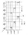
図1は、たとえば、不活性ガス流、反応物質A、反応物質B、及び、エネルギー源がいつオンにされたかなど、様々な処理パラメータに関して、CFD処理100における典型的な各フェーズの進行を時系列で示す。図1では、2つの蒸着サイクル110A及び110Bを示す。当業者には自明のことであるが、このCFD処理では、所望の厚さの膜を蒸着するために、任意の適当な数の蒸着サイクルを実行すればよい。CFD処理パラメータの例としては、以下に限定されるものではないが、不活性種及び反応種の流量、プラズマ出力及び周波数、紫外線波長、持続時間及び強度、基板温度及び処理ステーションの圧力が挙げられる。
FIG. 1 shows the progression of typical phases in the
「CFDサイクル」の概念は、本明細書における様々な実施形態の議論に関係する。一般に、サイクルは、表面堆積反応を一回実行するのに必要な最小の操作群である。1サイクルの結果、基板表面上に少なくとも部分的な膜層が生成される。典型的には、CFDサイクルは、基板表面に各反応物質を供給して吸着させ、次に、吸着された反応物質を反応させて部分的な膜層を形成するために必要な工程のみを含む。このサイクルは、反応物質の1つ又は副生成物を掃引(スイープ)する、及び/又は、蒸着される部分的な膜を処理するような特定の補助工程を備えるものでもよい。一般に、1サイクルには、1つの特有な一連操作のみが含まれる。たとえば、1サイクルは、以下の操作を含むものでもよい。(i)反応物質Aを供給し/吸着させる、(ii)反応物質Bを供給し/吸着させる、(iii)反応チャンバからBをスイープする、及び、(iv)活性化させることにより、AとBとの表面反応を促進させて、表面上に部分的な膜層を形成する。 The concept of “CFD cycle” relates to the discussion of various embodiments herein. In general, a cycle is the minimum set of operations required to perform a surface deposition reaction once. One cycle results in the creation of at least a partial film layer on the substrate surface. Typically, a CFD cycle includes only the steps necessary to supply and adsorb each reactant to the substrate surface and then react the adsorbed reactant to form a partial film layer. . This cycle may include certain auxiliary steps such as sweeping one of the reactants or by-products and / or treating the deposited partial film. In general, a cycle includes only one unique sequence of operations. For example, one cycle may include the following operations. (I) supply / adsorb reactant A, (ii) supply / adsorb reactant B, (iii) sweep B from the reaction chamber, and (iv) activate and The surface reaction with B is promoted to form a partial film layer on the surface.
図1に示すように、処理100のすべてのフェーズの間中、不活性ガスを流し続ける。反応物質Aの曝露フェーズ120Aにおいて、基板の露出表面が飽和するまで、制御された流量で処理ステーションに反応物質Aを供給する。反応物質Aは、任意の適当な堆積反応物質であればよく、たとえば、窒素含有反応物質である。図1に示す実施形態において、反応物質Aは、蒸着サイクル110A及び110Bを通して連続的に流される。気相反応を防ぐために膜前駆物質(反応物質)の曝露を別々に行う典型的なALD処理とは異なり、CFD処理の一部の実施形態において、反応物質A及びBは気相で混ざっていてもよい。反応物質Aの供給を開始し、供給を安定化させて基板を曝露させ、その後、供給を停止して、最後に反応器から除去するALD処理と比較して、処理ステーションに反応物質Aを連続的に供給することにより、反応物質Aの供給開始及び流量安定化にかかる時間を短縮する、又は、なくすことができる。図1に示す実施形態では、反応物質Aの曝露フェーズ120Aにおける反応物質Aの流量は一定の流量に設定されているが、当然のことながら、本発明の範囲内で、流量を変動させる等、反応物質Aの流量を任意の適当な流量とすることができる。一部の実施形態において、反応物質Aの曝露フェーズ120Aの持続時間は、反応物質Aに対する基板表面の飽和時間を超えるものであってもよい。たとえば、図1の実施形態では、反応物質Aの曝露フェーズ120Aには、反応物質Aの飽和後曝露時間130が含まれる。必要に応じて、反応物質Aの曝露フェーズ120Aにおいて、制御された流量の不活性ガスを流すようにしてもよい。不活性ガスの例としては、以下に限定されるものではないが、窒素、アルゴン及びヘリウムが挙げられる。処理ステーションの圧力及び/又は温度制御をしやすくするために、液体反応物質の蒸発を促進するために、反応物質をより速く供給するために、及び/又は、処理ステーション及び/又は処理ステーション配管から処理ガスを除去するためのスイープガスとして用いられるように、不活性ガスを供給するようにしてもよい。
As shown in FIG. 1, the inert gas continues to flow during all phases of the
図1に示す実施形態の反応物質Bの曝露フェーズ140Aにおいて、基板の露出表面が飽和するまで、制御された流量で処理ステーションに反応物質Bを供給する。この例では、反応物質Bは、たとえば、ケイ素含有反応物質でもよい。図1に示す実施形態では、反応物質Bの曝露フェーズ140Aにおける反応物質Bの流量は一定の流量に設定されているが、当然のことながら、本発明の範囲内で、流量を変動させる等、反応物質Bの流量を任意の適当な流量とすることができる。さらに、当然のことながら、反応物質Bの曝露フェーズ140Aにおける持続時間も任意の適当な持続時間に設定可能である。一部の実施形態において、反応物質Bの曝露フェーズ140Aの持続時間は、反応物質Bに対する基板表面の飽和時間を超えるものであってもよい。たとえば、図1の実施形態では、反応物質Bの曝露フェーズ140Aには、反応物質Bの飽和後曝露時間150が含まれる。
In the reactant
一部の実施形態において、表面に吸着された種Bが基板表面上で不連続な島状に点在する場合があり、この場合には、反応物質Bの表面飽和は難しい。様々な表面条件により、基板表面上における反応物質の核形成及び飽和が遅くなる可能性がある。たとえば、吸着された反応物質A及び/又はBにおいて放出されたリガンド(配位子)によって、一部の表面活性部位が阻害されて、反応物質Bをそれ以上吸着させることができなくなる場合がある。したがって、一部の実施形態において、反応物質Bの曝露フェーズ140Aの間中、処理ステーションへの反応物質の流量を調整する、及び/又は、反応物質Bの流れを離散的に脈動させることにより、反応物質Bの連続的な吸着層を提供するようにしてもよい。この方法では、一定流量の場合と比べて、反応物質Bを節約できる一方で、表面吸着及び脱離処理に余分な時間がかかる。さらに、あるいは、代わりに、一部の実施形態では、連続した反応物質Bの曝露の間に、1つ又は複数のスイープフェーズを設けるようにしてもよい。
In some embodiments, species B adsorbed on the surface may be scattered in discontinuous islands on the substrate surface, in which case the surface saturation of reactant B is difficult. Various surface conditions can slow the nucleation and saturation of reactants on the substrate surface. For example, the ligand released in the adsorbed reactants A and / or B may inhibit some of the surface active sites, making it impossible to further adsorb the reactant B. . Thus, in some embodiments, by adjusting the reactant flow rate to the processing station and / or discretely pulsing the reactant B flow during the reactant
一部の実施形態において、活性化の前に、スイープフェーズ160Aで、気相反応物質Bを処理ステーションから除去するようにしてもよい。処理ステーションをスイープ(掃引)することにより、反応物質Bがプラズマ活性化に対して不安定な場合に、又は、不要な種が形成される可能性がある場合に、気相反応を防ぐことができる。さらに、処理ステーションをスイープすることにより、膜内に残り膜の品質を低下させる恐れのある表面吸着リガンドを除去することができる。スイープガスの例としては、以下に限定されるものではないが、アルゴン、ヘリウム及び窒素が挙げられる。図1に示す実施形態において、不活性ガスの連続流が、スイープフェーズ160Aにおけるスイープガスとして機能する。一部の実施形態において、スイープフェーズ160Aは、処理ステーションを減圧にする1つ又は複数の減圧サブフェーズを備えるものでもよい。あるいは、当然のことながら、一部の実施形態では、スイープフェーズ160Aを省略することも可能である。
In some embodiments, the vapor phase reactant B may be removed from the processing station in a
スイープフェーズ160Aの持続時間は、任意の適当な持続時間でよい。一部の実施形態において、1つ又は複数のスイープガスの流量を増大させることによって、スイープフェーズ160Aの持続時間を短くするようにしてもよい。たとえば、種々の反応物質の熱力学的特性及び/又は処理ステーション及び/又は処理ステーション配管の幾何学的特性に応じてスイープガスの流量を調整して、スイープフェーズ160Aの持続時間を変更するようにしてもよい。非限定的な一例として、スイープガスの流量を調整することによって、スイープフェーズの持続時間を最適化するようにしてもよい。これにより、蒸着サイクルタイムを削減でき、基板スループットを向上させることができる。
The duration of
図1に示す実施形態の活性化フェーズ180Aでは、エネルギーを与えて、表面に吸着された反応物質Aと反応物質Bとの間の表面反応を活性化させる。たとえば、プラズマは、反応物質Aの気相分子を直接的に又は間接的に活性化させて、反応物質Aのラジカルを形成することができる。このようなラジカルが表面に吸着された反応物質Bと相互作用することにより、膜形成表面反応が生じる。別の例として、紫外線(UV)照射により、反応物質Aの気相分子を直接的に又は間接的に活性化させて、反応物質Aのラジカルを形成し、表面に吸着された反応物質Bと相互作用させるようにしてもよい。
In the
様々な実施形態において、活性化フェーズ180Aは、直接(in−situ)プラズマ、遠隔プラズマ、紫外線照射、可視光照射及びマイクロ波照射の1つ又は複数を含むものでもよい。活性化フェーズ180Aは、蒸着サイクル110Aの最後のフェーズであり、図1の実施形態では、これに続いて、蒸着サイクル110Bが実施される。蒸着サイクル110Bは、反応物質Aの曝露フェーズ120Bで開始され、B曝露フェーズ140B、スイープフェーズ160B及びプラズマ活性化フェーズ180Bがこれに続く。
In various embodiments, the
一部の実施形態において、活性化フェーズ180Aで形成されるプラズマは、基板表面のすぐ上方で形成されるものでもよい。この場合には、プラズマ密度を高めることができ、反応物質Aと反応物質Bとの間の表面反応速度を増大させることができる。たとえば、2枚の容量結合プレートを用いて低圧ガスに高周波(RF:radio frequency)場を印加することによって、CFD処理用のプラズマを生成することができる。任意の適当なガスを用いてプラズマを形成可能である。この例では、アルゴンやヘリウムなどの不活性ガスを、反応物質A、すなわち、窒素含有反応物質と共に用いて、プラズマを形成するようにしてもよい。RF場によってプレート間でガスをイオン化することによりプラズマを点火して、プラズマ放電領域において自由電子を形成する。これらの電子は、RF場によって加速されて、気相の反応物質分子に衝突するものでもよい。このような電子が反応物質分子に衝突すると、蒸着処理に関与するラジカル種が形成される。当然のことながら、RF場は、任意の適当な電極を介して結合されるものでもよい。電極の非限定的な例として、処理ガス分配シャワーヘッド及び基板支持台座が挙げられる。当然のことながら、RF場をガスに容量結合させる方法以外の1つ又は複数の適当な方法でCFD処理用のプラズマを形成するものでもよい。
In some embodiments, the plasma formed in the
一部の実施形態において、活性化フェーズ180Aで形成されるプラズマは、遠隔プラズマ源によって形成されるものでもよい。一部の実施形態において、遠隔プラズマ源からの活性種は、基板を収容するチャンバに導入されて反応物質と相互作用するものでもよい。一部の実施形態において、これらの活性種は、イオン、電子、ラジカル及び高エネルギー分子を含む。一部の実施形態において、チャンバに導入される活性種は、チャンバに導入される前の再結合により、イオン及び/又は電子をほとんど持たないラジカルを含む。一部の実施形態において、イオンフィルタを用いるようにしてもよい。遠隔プラズマ源に供給されて活性種を与えるガスの例としては、アルゴン、ヘリウム、アンモニア、水素及び酸素が挙げられる。
In some embodiments, the plasma formed in the
一部の実施形態において、活性化フェーズ180Aは、紫外線源からの照射への曝露を含むものでもよい。広帯域紫外線源及び狭帯域紫外線源を含む任意の適当な紫外線源を用いることができる。たとえば、紫外線に曝露させることにより、蒸着処理に関与するラジカル種を形成するようにしてもよい。一部の実施形態において、紫外線源は、1つ以上の反応物質を励起するように、又は、反応を活性化するように選択された1つ又は複数の波長の光を放出するものでもよい。一部の実施形態において、反応物質が反応チャンバ内にある場合に、紫外線に曝露するようにしてもよい。たとえば、紫外線源をチャンバ内に載置するようにしてもよいし、チャンバの外側に載置するようにしてもよい。紫外線が窓(ウインドウ)を透過して反応物質に到達するようにしてもよい。別の実施形態において、チャンバに反応物質を導入する前に、紫外線に曝露するようにしてもよい。たとえば、チャンバに注入される前に紫外線照射に反応物質を曝露させて、ラジカル及び/又は他の活性種をチャンバに導入するようにしてもよい。これらの実施形態において、活性化フェーズ180Aは、反応物質曝露フェーズと同時に実施されるものでもよいし、反応物質曝露フェーズに重なるように実施されるものでもよい。このような処理の例を、後述する。
In some embodiments, the
一部の実施形態において、活性化フェーズ180Aは、可視光源からの照射への曝露を含むものでもよい。たとえば、蒸着処理に関与するラジカル種を形成するようにしてもよい。一部の実施形態において、可視光源は、1つ以上の反応物質を励起するように、又は、反応を活性化するように選択された1つ又は複数の波長の光を放出するものでもよい。一部の実施形態において、反応物質が反応チャンバ内にある場合に、可視光に曝露するようにしてもよい。たとえば、光源をチャンバ内に載置するようにしてもよいし、チャンバの外側に載置するようにしてもよい。可視光が窓を透過して反応物質に到達するようにしてもよい。別の実施形態において、チャンバに反応物質を導入する前に、反応物質を励起する可視光に曝露するようにしてもよい。たとえば、チャンバに注入する前に反応物質を照射に曝露して、ラジカル及び/又は他の活性種をチャンバに導入するようにしてもよい。これらの実施形態において、活性化フェーズ180Aは、反応物質曝露フェーズと同時に実施されるものでもよいし、反応物質曝露フェーズに重なるように実施されるものでもよい。このような処理の例を、後述する。
In some embodiments, the
一部の実施形態において、活性化フェーズ180Aは、マイクロ波照射への曝露を含むものでもよい。たとえば、蒸着処理に関与するラジカル種を形成するようにしてもよい。一部の実施形態において、マイクロ波源は、1つ以上の反応物質を励起するように、又は、反応を活性化するように選択された1つ又は複数の波長で光を放出するものでもよい。一部の実施形態において、反応物質が反応チャンバ内にある場合に、マイクロ波に曝露するようにしてもよい。たとえば、マイクロ波源をチャンバ内に載置するようにしてもよいし、チャンバの外側に載置するようにしてもよい。マイクロ波が窓を透過して反応物質に到達するようにしてもよい。別の実施形態において、チャンバに反応物質を導入する前に、反応物質を励起するマイクロ波に曝露するようにしてもよい。たとえば、チャンバに注入する前に反応物質を照射に曝露して、ラジカル及び/又は他の活性種をチャンバに導入するようにしてもよい。これらの実施形態において、活性化フェーズ180Aは、反応物質曝露フェーズと同時に実施されるものでもよいし、反応物質曝露フェーズに重なるように実施されるものでもよい。このような処理の例を、後述する。
In some embodiments, the
一部の実施形態において、活性化フェーズ180Aは、上述した活性化モードの1つまたは複数を含むものでもよい。活性化フェーズ180Aの持続時間は、任意の適当な持続時間であればよい。一部の実施形態において、活性化フェーズ180Aの持続時間を、活性化されたラジカルがすべての露出基板表面及び吸着質と相互作用するのに必要な時間を超える時間として、基板表面上に連続膜を形成するようにしてもよい。たとえば、図1に示す実施形態では、活性化フェーズ180Aには、飽和後曝露時間190が含まれる。
In some embodiments, the
一部の実施形態において、活性化エネルギー曝露時間を延ばすこと、及び/又は、複数の曝露フェーズを実施することにより、蒸着膜のバルク部分及び/又は表面近傍部分の反応後処理を行うようにしてもよい。一つの実施形態において、表面汚染を削減することによって、反応物質Aを吸着する表面の準備を行うようにしてもよい。たとえば、ケイ素含有反応物質と窒素含有反応物質との反応から形成される窒化ケイ素膜が、次段の反応物質の吸着に抗する表面を有するようにしてもよい。窒化ケイ素表面をプラズマ又は他の活性化エネルギーで処理することにより、水素結合を形成し、次段の吸着及び反応を容易にするようにしてもよい。プラズマ処理に加え、このような処理には、電磁波放射処理、熱処理(たとえば、焼きなまし又は高温パルス)などが含まれる。このような処理のうち任意の処理を単独で実行するものでもよいし、又は、プラズマ処理を含む他の処理と組み合わせて実行するようにしてもよい。特定の実施形態において、処理は、紫外線に膜を曝露することを含む。以下で説明するように、特定の実施形態において、in situ(その場)で(すなわち、膜形成の間に)膜に紫外線を照射する、又は、膜の後蒸着を行う。このような処理は、欠陥構造を削減する又はなくすとともに、電気的性能を向上させることができる。 In some embodiments, post-reaction treatment of the bulk portion and / or near-surface portion of the deposited film may be performed by extending the activation energy exposure time and / or performing multiple exposure phases. Also good. In one embodiment, the surface to adsorb reactant A may be prepared by reducing surface contamination. For example, a silicon nitride film formed from a reaction between a silicon-containing reactant and a nitrogen-containing reactant may have a surface that resists adsorption of the next-stage reactant. The silicon nitride surface may be treated with plasma or other activation energy to form hydrogen bonds to facilitate subsequent adsorption and reaction. In addition to plasma treatment, such treatment includes electromagnetic radiation treatment, heat treatment (eg, annealing or high temperature pulse), and the like. Of these processes, an arbitrary process may be executed alone, or may be executed in combination with other processes including a plasma process. In certain embodiments, the treatment includes exposing the film to ultraviolet light. As described below, in certain embodiments, the film is irradiated with ultraviolet light or post-deposition of the film in situ (ie, during film formation). Such processing can reduce or eliminate defect structures and improve electrical performance.
ある特定の実施形態において、紫外線処理をプラズマ処理とを併用するようにしてもよい。これら2つの処理は、同時に行ってもよいし、連続的に行ってもよい。連続的に行う場合には、いずれの処理を先に行ってもよい。同時に行う場合には、別々の発生源(たとえば、プラズマ用にRF電源、また、紫外線用にランプ)を用いるものでもよいし、副生成物として紫外線を発生させるヘリウムプラズマのような単一の発生源を用いるものでもよい。 In a specific embodiment, ultraviolet treatment may be used in combination with plasma treatment. These two processes may be performed simultaneously or continuously. When performing continuously, any process may be performed first. If performed simultaneously, separate sources (eg, RF power source for plasma and lamp for ultraviolet light) may be used, or a single generation such as helium plasma that generates ultraviolet light as a by-product. A source may be used.
一部の実施形態において、プラズマ又は他の活性化エネルギーのパラメータを変更することによって、膜応力、誘電率、屈折率、エッチング速度等の膜特性を調整するようにしてもよい。 In some embodiments, film properties such as film stress, dielectric constant, refractive index, etch rate, etc. may be adjusted by changing plasma or other activation energy parameters.
本明細書で説明する多くの実施例では2つの反応物質(A及びB)が用いられているが、当然のことながら、本発明の範囲内で任意の適当な数の反応物質を用いることができる。一部の実施形態において、単一の反応物質と表面反応に対してプラズマエネルギーを供給するための不活性ガスとを用いるようにしてもよい。あるいは、複数の反応物質を用いて、膜を蒸着させる実施形態でもよい。たとえば、一部の実施形態において、ケイ素含有反応物質と1つ若しくは複数の窒素含有反応物質との反応により、又は、1つ若しくは複数のケイ素含有反応物質と単一の窒素含有反応物質との反応により、又は、複数のケイ素含有反応物質と複数の窒素含有反応物質との反応により、窒化ケイ素膜を形成するものでもよい。 In many of the embodiments described herein, two reactants (A and B) are used, but it will be appreciated that any suitable number of reactants may be used within the scope of the present invention. it can. In some embodiments, a single reactant and an inert gas for supplying plasma energy for the surface reaction may be used. Alternatively, an embodiment in which a film is deposited using a plurality of reactants may be used. For example, in some embodiments, by reaction of a silicon-containing reactant with one or more nitrogen-containing reactants, or reaction of one or more silicon-containing reactants with a single nitrogen-containing reactant. Alternatively, a silicon nitride film may be formed by a reaction between a plurality of silicon-containing reactants and a plurality of nitrogen-containing reactants.
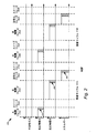
図2は、たとえば、不活性ガス流、反応物質A、反応物質B、及び、エネルギー源がいつオンにされたかなど、様々な処理パラメータに関して、処理200における各フェーズの進行の別の例を時系列で示す。図2では、2つの蒸着サイクル210A及び210Bを示す。当業者には自明のことであるが、この処理では、所望の厚さの膜を蒸着するために、任意の適当な数の蒸着サイクルを実行すればよい。処理パラメータの例としては、以下に限定されるものではないが、不活性種及び反応種の流量、プラズマ出力及び周波数、紫外線波長、強度、持続時間、基板温度及び処理ステーションの圧力が挙げられる。
FIG. 2 illustrates another example of the progress of each phase in
図2に示すように、処理200のすべてのフェーズの間中、不活性ガスを流し続ける。ただし、他の実施形態において、不活性ガスを流し続けなくてもよい。反応物質Aの曝露フェーズ220Aにおいて、基板の露出表面が飽和するまで、制御された流量で処理ステーションに反応物質Aを供給する。反応物質Aは、任意の適用な堆積反応物質であればよく、たとえば、ケイ素含有反応物質である。図2に示す実施形態では、反応物質Aの曝露フェーズ220Aにおける反応物質Aの流量は一定の流量に設定されているが、当然のことながら、本発明の範囲内で、流量を変動させる等、反応物質Aの流量を任意の適当な流量とすることができる。一部の実施形態において、反応物質Aの曝露フェーズ220Aの持続時間は、反応物質Aに対する基板表面の飽和時間を超えるものであってもよい。たとえば、図2の実施形態では、反応物質Aの曝露フェーズ220Aには、反応物質Aの飽和後曝露時間230が含まれる。必要に応じて、反応物質Aの曝露フェーズ220Aにおいて、制御された流量の不活性ガスを流すようにしてもよい。不活性ガスの例としては、以下に限定されるものではないが、窒素、アルゴン及びヘリウムが挙げられる。処理ステーションの圧力及び/又は温度制御をしやすくするために、液体反応物質の蒸発を促進するために、反応物質をより速く供給するために、及び/又は、処理ステーション及び/又は処理ステーション配管から処理ガスを除去するためのスイープガスとして用いられるように、不活性ガスを供給するようにしてもよい。
As shown in FIG. 2, the inert gas continues to flow during all phases of the
一部の実施形態において、B曝露フェーズ240Aの前に、スイープフェーズ260Aで、気相反応物質Aを処理ステーションから除去するようにしてもよい。処理ステーションをスイープすることにより、基板表面上に吸着されていない反応物質Aをパージすることができる。スイープガスの例としては、以下に限定されるものではないが、アルゴン、ヘリウム及び窒素が挙げられる。図2に示す実施形態において、不活性ガスの連続流が、スイープフェーズ260Aにおけるスイープガスとして機能する。一部の実施形態において、スイープガスは、スイープフェーズの間だけ供給されるものでもよい。一部の実施形態において、スイープフェーズ260Aは、処理ステーションを減圧にする1つ又は複数の減圧サブフェーズを備えるものでもよい。あるいは、当然のことながら、一部の実施形態では、スイープフェーズ260Aを省略することも可能である。
In some embodiments, the vapor phase reactant A may be removed from the processing station in a
図2に示す実施形態の反応物質Bの曝露フェーズ240Aにおいて、基板の露出表面が飽和するまで、制御された流量で処理ステーションに反応物質Bを供給する。この例では、反応物質Bは、たとえば、窒素含有反応物質でもよい。図2に示す実施形態では、反応物質Bの曝露フェーズ240Aにおける反応物質Bの流量は一定の流量に設定されているが、当然のことながら、本発明の範囲内で、流量を変動させる等、反応物質Bの流量を任意の適当な流量とすることができる。さらに、当然のことながら、反応物質Bの曝露フェーズ240Aにおける持続時間も任意の適当な持続時間に設定可能である。一部の実施形態において、反応物質Bの曝露フェーズ240Aの持続時間は、反応物質Bに対する基板表面の飽和時間を超えるものであってもよい。たとえば、図2の実施形態では、反応物質Bの曝露フェーズ240Aには、反応物質Bの飽和後曝露時間250が含まれる。
In the reactant
図2に示す実施形態の活性化フェーズ280Aでは、エネルギーを与えて、表面に吸着された反応物質Aと反応物質Bとの間の表面反応を活性化させる。たとえば、プラズマは、反応物質Bの気相分子を直接的に又は間接的に活性化させて、反応物質Bのラジカルを形成することができる。このようなラジカルが表面に吸着された反応物質Aと相互作用することにより、膜形成表面反応が生じる。別の例として、紫外線(UV)照射により、反応物質Bの気相分子を直接的に又は間接的に活性化させて、反応物質Bのラジカルを形成し、表面に吸着された反応物質Aと相互作用させるようにしてもよい。図2に示すB曝露フェーズ240Aは活性化フェーズ280Aの前に終了しているが、一部の実施形態において、この2つのフェーズが重なるように実行するものでもよい。様々な実施形態において、活性化フェーズ280Aは、上述したように、直接(in−situ)プラズマ、遠隔プラズマ、紫外線照射、可視光照射及びマイクロ波照射の1つ又は複数を含むものでもよい。
In the
活性化フェーズ280Aの持続時間は、任意の適当な持続時間であればよい。一部の実施形態において、活性化フェーズ280Aの持続時間を、活性化されたラジカルがすべての露出基板表面及び吸着質と相互作用するのに必要な時間を超える時間として、基板表面上に連続膜を形成するようにしてもよい。たとえば、図2に示す実施形態では、活性化フェーズ280Aには、飽和後曝露時間290が含まれる。
The duration of
図2の実施形態では、活性化フェーズ280Aの後に、スイープフェーズ270Aが実施される。一部の実施形態において、スイープフェーズ270Aにおいて、気相反応物質Bを処理ステーションから除去するようにしてもよい。処理ステーションをスイープすることにより、気相反応物質Bのみでなく、不要な副生成物及び/又は汚染物質をパージすることができる。スイープガスの例としては、以下に限定されるものではないが、アルゴン、ヘリウム及び窒素が挙げられる。図2に示す実施形態において、不活性ガスの連続流が、スイープフェーズ270Aにおけるスイープガスとして機能する。ただし、スイープガスは他の方法で供給されるものでもよい。スイープフェーズ270Aは、処理ステーションを減圧にする1つ又は複数の減圧サブフェーズを備えるものでもよい。あるいは、当然のことながら、一部の実施形態では、スイープフェーズ270Aを省略することも可能である。スイープフェーズ270Aは、蒸着サイクル210Aの最後のフェーズであり、図2の実施形態では、これに続いて、蒸着サイクル210Bが実施される。蒸着サイクル210Bは、反応物質Aの曝露フェーズ220Bで開始され、スイープフェーズ260B,B曝露フェーズ240B、プラズマ活性化フェーズ280B及びスイープフェーズ270Bがこれに続く。
In the embodiment of FIG. 2, a
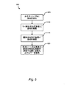
図3は、一実施形態の方法の概要を示す処理フロー図300である。305で、反応チャンバに基板を提供する。310で、必要に応じて、熱浸漬(サーマルソーク)を実施して、基板を所望の温度まで加熱するようにしてもよい。一つの実施形態において、本明細書で説明する方法のうち任意の方法を用いて、基板を約50℃〜約550℃に、より具体的には、約300℃〜約450℃に、たとえば、約350℃〜約400℃に加熱する。次に、315で、チャンバに1つ又は複数のケイ素含有前駆物質を供給する。一部の実施形態において、工程415で、ケイ素含有反応物質に加えて、(たとえば、酸化ケイ素又は酸窒化ケイ素の蒸着のための)酸化剤及び/又は(たとえば、窒化ケイ素又は酸窒化ケイ素の蒸着のための)窒素含有前駆物質などの共反応物質を供給するようにしておよい。基板表面上に、1つ又は複数のケイ素含有前駆物質が、たとえば、化学吸着や物理吸着によって、吸着されるものでもよい。320で、必要に応じて、パージ操作を行い、基板表面上に吸着された物質を残すようにしてもよい。325で、紫外線エネルギーで、表面に結合した分子を活性化することができる。様々な実施形態において、1つ又は複数の表面に結合したケイ素含有反応物質及び表面に結合した共反応物質と紫外線エネルギーが相互作用するものでもよい。一部の実施形態において、1つ又は複数の反応物質上の1つ又は複数のリガンドと相互作用するように、紫外線波長又は紫外線波長領域を選択するようにしてもよい。紫外線照射の結果、SiN、SiC、SiO2、SiCN、SiON又はSiONCなど、所望のケイ素含有膜を形成する反応が活性化される。たとえば、炭素含有ケイ素前駆物質及び窒素含有共反応物質を用いて、SiCNを形成するようにしてもよい。酸素含有及び炭素含有ケイ素前駆物質及び窒素含有共反応物質を用いて、SiONCを形成するようにしてもよい。一部の実施形態において、共反応物質は、SiOを蒸着するのに利用可能な酸化剤でもよい。たとえば、酸素含有及び炭素含有ケイ素前駆物質及び酸化剤を用いて、酸化ケイ素を形成するようにしてもよい。処理300は、続いて、必要に応じて、330で、パージを行って、SiN、SiO2、SiCN、SiON、SiONC又はその他の膜の層のみを基板上に残すようにしてもよい。工程315〜330を繰り返して、所望の厚さの膜を形成するようにしてもよい。
FIG. 3 is a process flow diagram 300 that outlines the method of an embodiment. At 305, a substrate is provided to the reaction chamber. At 310, if necessary, a thermal soak may be performed to heat the substrate to a desired temperature. In one embodiment, using any of the methods described herein, the substrate is from about 50 ° C. to about 550 ° C., more specifically from about 300 ° C. to about 450 ° C., for example, Heat to about 350 ° C to about 400 ° C. Next, at 315, the chamber is provided with one or more silicon-containing precursors. In some embodiments, in
特定の実施形態において、工程325において、紫外線エネルギーに加えて、又は、紫外線エネルギーに代えて、他のエネルギー源を用いるようにしてもよい。たとえば、工程325において、紫外線照射をプラズマと共に用いるようにしてもよい。一部の実施形態において、紫外線照射の代わりに、又は、紫外線照射に加えて、マイクロ波照射及び/又は可視光照射を用いるようにしてもよい。
In certain embodiments, other energy sources may be used in
図4は、一実施形態の方法の概要を示す処理フロー図400である。405チャンバに基板を提供する。410で、必要に応じて、上述したような熱浸漬を行う。次に、415で、チャンバに1つ又は複数のケイ素含有前駆物質を供給する。基板表面上に、1つ又は複数の前駆物質が、たとえば、化学吸着や物理吸着によって、吸着されるものでもよい。処理400は、続いて、420で、必要に応じて、パージを行って、基板上に吸着物質の層を残すようにしてもよい。様々な実施形態において、この相は、表面に結合したケイ素含有反応物質を含むものでもよい。425で、紫外線波長エネルギーを用いて、共反応物質前駆物質又は前駆物質流を活性化するようにしてもよい。たとえば、反応チャンバ内で、又は、反応チャンバの上流で、気相において窒素含有反応物質及び/又は酸化剤を活性化するようにしてもよい。一部の実施形態において、表面吸着ケイ素含有反応物質と気相共反応物質の両方を活性化させるようにしてもよい。紫外線照射の結果、SiN、SiCN、SiC、SiO、SiON又はSiONCなど、所望のケイ素含有膜を形成する反応が活性化される。処理400は、続いて、必要に応じて、430で、パージを行って、SiN、SiCN、SiC、SiO、SiON、SiONC又はその他のケイ素含有膜の層のみを基板上に残すようにしてもよい。工程415〜430を繰り返して、所望の厚さの膜を形成するようにしてもよい。
FIG. 4 is a process flow diagram 400 illustrating an overview of the method of one embodiment. A substrate is provided in the 405 chamber. At 410, thermal dipping as described above is performed as necessary. Next, at 415, the chamber is provided with one or more silicon-containing precursors. One or more precursors may be adsorbed on the substrate surface, for example by chemical adsorption or physical adsorption.
図5は、ケイ素含有膜を形成するための特定の実施形態における処理フローの例を示す。当然のことながら、図5に示すような処理によって、用いられる特定のケイ素含有反応物質と窒素含有反応物質とに応じて、SiCN膜、SiONC膜及びSiON膜を形成することができる。SiONC膜及びSiON膜を形成する場合には、工程515で、窒素含有反応物質に加えて、酸素含有共反応物質を用いるようにしてもよい。さらに、図5に示すような処理によって、工程515で、たとえば、窒素含有反応物質の代わりに酸素含有反応物質を用いることによりSiOを形成することができる。酸素含有共反応物質の例としてO2が挙げられる。
FIG. 5 shows an example of a process flow in a particular embodiment for forming a silicon-containing film. As a matter of course, the SiCN film, the SiONC film, and the SiON film can be formed according to the specific silicon-containing reactant and the nitrogen-containing reactant used by the process as shown in FIG. When forming the SiONC film and the SiON film, in
処理500が開始されると、まず505で、チャンバに基板が提供される。この基板は、ケイ素含有膜が基板上に必要とされる任意の適当な基板でよい。たとえば、この基板は、半製品の集積回路、フラッシュメモリ又は相変化メモリ基板でもよい。提供される基板は、裸ケイ素基板等の裸基板でもよいし、1つ又は複数の層が蒸着された基板でもよい。SiN又はその他のケイ素含有膜が蒸着されるべき表面は、たとえば、ケイ素、ポリシリコン、銅、チタン、タングステン、二酸化ケイ素又はゲルマニウム‐アンチモン‐テルル(GST)合金でもよいし、これらを含むものでもよい。一部の実施形態において、表面は、1つ又は複数の凸部フィーチャ又は凹部フィーチャを有するものでもよい。1つ又は複数の凸部フィーチャのアスペクト比は、たとえば、2:1〜10:1でもよい。510で、ケイ素含有反応物質に基板を曝露させる。一部の実施形態において、工程510は非プラズマ処理である。一部の実施形態では、たとえば、約5トール〜50トールの間の第1の圧力まで反応器を加圧するようにしてもよい。特定の実施形態において、工程510の間の圧力は、約20トールである。所望の実施形態において、この範囲外の圧力を用いるようにしてもよい。ケイ素含有反応物質が、基板表面上に吸着される。表面上に所望量のケイ素含有反応物質を吸着後、ケイ素含有反応物質流を停止するようにしてもよい(図示しない)。515で、1つ又は複数の窒素含有反応物質に基板を曝露させる。520で、気相に窒素含有反応物質が存在する間に、活性エネルギーを与えて、基板上にSiN膜又はその他のケイ素含有及び窒素含有膜を形成する。様々な実施形態において、窒素含有反応物質は、(たとえば、図1の反応物質Aのように)処理の間ずっと連続的に流されるものでもよいし、(たとえば、図2の反応物質Bのように)断続的に流されるものでもよい。前者の場合、一部の実施形態において、工程520を断続的に実行するものでもよい。一方、後者の場合、一部の実施形態において、窒素含有反応物質が存在しない間も、エネルギー源をオンのままにしておくものでもよい。
When the
様々な実施形態において、工程520は、直接(in−situ)プラズマ、遠隔プラズマ、紫外線照射、可視光照射及びマイクロ波照射の1つ又は複数を含むものでもよい。
In various embodiments,
たとえば、一部の実施形態において、工程520は、基板表面の上方に直接プラズマを直接形成するようにしてもよい。これにより、プラズマ密度が高まり、反応物質間の表面反応速度が増大する。たとえば、2枚の容量結合プレートを用いて、低圧ガスに高周波(RF)場を印加することにより、プラズマを生成するものでもよい。任意の適当なガスを用いて、プラズマを形成するようにしてもよい。RF場によってプレート間でガスをイオン化することによりプラズマを点火して、プラズマ放電領域において自由電子を形成する。これらの電子は、RF場によって加速されて、気相の反応物質分子に衝突するものでもよい。このような電子が反応物質分子に衝突すると、蒸着処理に関与するラジカル種が形成される。当然のことながら、RF場は、任意の適当な電極を介して結合されるものでもよい。電極の非限定的な例として、処理ガス分配シャワーヘッド及び基板支持台座が挙げられる。当然のことながら、RF場をガスに容量結合させる方法以外の1つ又は複数の適当な方法でプラズマを形成するものでもよい。
For example, in some embodiments,
一部の実施形態において、520で、遠隔生成されたプラズマ又は下流プラズマにより、活性化エネルギーのすべて又は一部を提供するようにしてもよい。一部の実施形態において、遠隔プラズマ源からの活性種は、基板を収容するチャンバに導入されて反応物質と相互作用するものでもよい。一部の実施形態において、これらの活性種は、イオン、電子、ラジカル及び高エネルギー分子を含む。一部の実施形態において、チャンバに導入される活性種は、チャンバに導入される前の再結合により、イオン及び/又は電子をほとんど持たないラジカルを含む。一部の実施形態において、遠隔プラズマ発生装置に窒素含有反応物質又はその他の共反応物質を提供することによって、工程515の前に、工程520を実行するようにしてもよい。たとえば、遠隔プラズマ源にアンモニア共反応物質を供給して、SiN膜、SiCN膜、SiOCN膜及びSiON膜を形成するようにしてもよい。別の例として、遠隔プラズマ源に酸素を供給して、SiO膜、SiOCN膜及びSiON膜を形成するようにしてもよい。
In some embodiments, at 520, all or part of the activation energy may be provided by remotely generated plasma or downstream plasma. In some embodiments, active species from a remote plasma source may be introduced into a chamber containing the substrate and interact with the reactants. In some embodiments, these active species include ions, electrons, radicals, and high energy molecules. In some embodiments, the active species introduced into the chamber includes radicals that have few ions and / or electrons due to recombination prior to introduction into the chamber. In some embodiments,
一部の実施形態において、工程520は、紫外線源からの照射への曝露を含むものでもよい。広帯域紫外線源及び狭帯域紫外線源を含む任意の適当な紫外線源を用いることができる。たとえば、紫外線に曝露させることにより、蒸着処理に関与するラジカル種を形成するようにしてもよい。一部の実施形態において、紫外線源は、1つ以上の反応物質を励起するように、又は、反応を活性化するように選択された1つ又は複数の波長の光を放出するものでもよい。一部の実施形態において、窒素含有反応物質が反応チャンバ内にある場合に、紫外線に曝露するようにしてもよい。たとえば、紫外線源をチャンバ内に載置するようにしてもよいし、チャンバの外側に載置するようにしてもよい。紫外線が窓を透過して反応物質に到達するようにしてもよい。別の実施形態において、チャンバに窒素含有反応物質を導入する前に、紫外線に曝露するようにしてもよい。たとえば、チャンバに注入される前に紫外線照射に反応物質を曝露させて、ラジカル及び/又は他の活性種をチャンバに導入するようにしてもよい。
In some embodiments,
様々な実施形態において、紫外線照射は、共反応物質又はその他の種を活性化するように選択される広帯域紫外線でも狭帯域紫外線でもよい。たとえば、アンモニア並びに第一級アミン、第二級アミン及び第三級アミンを活性化するために利用可能な波長は、約240nm未満でもよく、酸素を活性化するために利用可能な波長は約300nm未満でもよい。強度の例としては、広帯域源の場合には、紫外線領域全体にわたって、約0.5W/cm2でもよく、また、単一の波長エキシマの場合には、約10mW/cm2でもよい。 In various embodiments, the UV radiation can be broadband UV or narrow band UV selected to activate the co-reactant or other species. For example, the wavelength available to activate ammonia and primary, secondary and tertiary amines may be less than about 240 nm, and the wavelength available to activate oxygen is about 300 nm. It may be less. Examples of intensities may be about 0.5 W / cm 2 over the entire ultraviolet region for a broadband source, and about 10 mW / cm 2 for a single wavelength excimer.
一部の実施形態において、工程520は、可視光源からの照射への曝露を含むものでもよい。たとえば、蒸着処理に関与するラジカル種を形成するようにしてもよい。一部の実施形態において、可視光源は、1つ以上の反応物質を励起するように、又は、反応を活性化するように選択された1つ又は複数の波長の光を放出するものでもよい。一部の実施形態において、窒素含有反応物質が反応チャンバ内にある場合に、可視光に曝露するようにしてもよい。たとえば、光源をチャンバ内に載置するようにしてもよいし、チャンバの外側に載置するようにしてもよい。可視光が窓を透過して反応物質に到達するようにしてもよい。別の実施形態において、チャンバに反応物質を導入する前に、窒素含有反応物質を励起する可視光に曝露するようにしてもよい。たとえば、チャンバに注入する前に反応物質を照射に曝露して、ラジカル及び/又は他の活性種をチャンバに導入するようにしてもよい。
In some embodiments,
一部の実施形態において、工程520は、マイクロ波照射への曝露を含むものでもよい。たとえば、蒸着処理に関与するラジカル種を形成するようにしてもよい。一部の実施形態において、マイクロ波源は、1つ以上の反応物質を励起するように、又は、反応を活性化するように選択された1つ又は複数の波長で光を放出するものでもよい。一部の実施形態において、窒素含有反応物質が反応チャンバ内にある場合に、マイクロ波に曝露するようにしてもよい。たとえば、マイクロ波源をチャンバ内に載置するようにしてもよいし、チャンバの外側に載置するようにしてもよい。マイクロ波が窓を透過して反応物質に到達するようにしてもよい。別の実施形態において、チャンバに反応物質を導入する前に、窒素含有反応物質を励起するマイクロ波に曝露するようにしてもよい。たとえば、チャンバに注入する前に反応物質を照射に曝露して、ラジカル及び/又は他の活性種をチャンバに導入するようにしてもよい。
In some embodiments,
一部の実施形態において、反応器内の圧力を周期的に変化させて、工程510の間の圧力よりも工程515及び/又は工程520の間の圧力が低くなるようにする。たとえば、これらの工程の間の圧力は、約1トール〜約5トールでもよく、たとえば、2トールである。一部の実施形態において、工程520の後で、窒素含有反応物質の流れを停止するようにしてもよい(図示しない)。一部の実施形態において、ケイ素含有反応物質及び/又は窒素含有反応物質をパージするようにしてもよい。工程510〜520を1回又は複数回繰り返すことにより、SiN層又はその他のケイ素含有層を堆積させるようにしてもよい。これらの工程を繰り返して、一つの実施形態において、約1nm〜約100nmの厚さの、また、別の実施形態において、約5nm〜約50nmの厚さの、さらに別の実施形態において、約5nm〜約30nmの厚さの、コンフォーマルな層を基板上に形成する。
In some embodiments, the pressure in the reactor is periodically changed so that the pressure during
一つの実施形態において、本明細書で説明する方法のうち任意の方法を用いて、基板を約50℃〜約550℃に、より具体的には、約300℃〜約450℃に、たとえば、約350℃〜約400℃に加熱する。一つの実施形態において、蒸着の間ずっと、基板を加熱する。別の実施形態において、蒸着の間、又は、焼きなましのような蒸着工程の後で、基板を周期的に加熱する。 In one embodiment, using any of the methods described herein, the substrate is from about 50 ° C. to about 550 ° C., more specifically from about 300 ° C. to about 450 ° C., for example, Heat to about 350 ° C to about 400 ° C. In one embodiment, the substrate is heated throughout the deposition. In another embodiment, the substrate is periodically heated during the deposition or after a deposition process such as annealing.
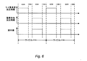
図6〜図13は、たとえば、ケイ素含有前駆物質流、窒素含有反応物質及び紫外線源の強度などの様々な処理パラメータに関して、1つ又は2つのSiN蒸着サイクルの進行の例を時系列で示す。不活性ガス流など、他に存在する可能性のあるパラメータは、説明を容易にするために省略してある。図6〜図13では、主にSiN膜に関して説明するが、当然のことながら、窒素含有反応物質に加えて、又は、窒素含有反応物質に代えて、他の反応物質を用いて、たとえば、SiO2、SiCN又はSiONCを形成することができる。同様に、当然のことながら、図6〜図13に示すような処理によって、用いられる特定のケイ素含有反応物質及び窒素含有反応物質に応じて、SiCN膜、SiOCN膜及びSiON膜を形成することができる。また、図6〜図13では、紫外線エネルギーに関して説明するが、当然のことながら、紫外線エネルギーに加えて、又は、紫外線エネルギーに代えて、上述したような1つ又は複数の他のエネルギー源を用いることができる。
6-13 show, in time series, examples of progress of one or two SiN deposition cycles for various process parameters such as, for example, silicon-containing precursor streams, nitrogen-containing reactants, and UV source intensity. Other parameters that may exist, such as an inert gas stream, are omitted for ease of explanation. 6 to 13, the SiN film will be mainly described. However, as a matter of course, in addition to the nitrogen-containing reactant or in place of the nitrogen-containing reactant, another reactant is used, for example,
特定の実施形態において、ケイ素含有反応物質は紫外線透過性であり、窒素含有反応物質は紫外線で活性化されるものでもよい。特定の他の実施形態において、ケイ素含有反応物質は、紫外線で活性化可能なリガンドを含むものでもよい。たとえば、約240nm未満の波長を持つ紫外線照射でNH3を活性化可能であり、また、約240nm未満の紫外線照射でO2含有リガンドを活性化可能である。約200nm未満の波長を持つ紫外線照射でSiH4及びこの誘導体の大部分を活性化可能である。 In certain embodiments, the silicon-containing reactant may be UV transmissive and the nitrogen-containing reactant may be UV activated. In certain other embodiments, the silicon-containing reactant may include a UV activatable ligand. For example, NH 3 can be activated by UV irradiation with a wavelength of less than about 240 nm, and O 2 -containing ligands can be activated by UV irradiation of less than about 240 nm. SiH 4 and most of its derivatives can be activated by UV irradiation with a wavelength of less than about 200 nm.
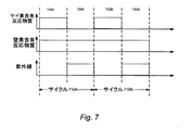
まず、図6は、2つのサイクル610A及び610Bを示し、各サイクルで、SiN層が蒸着される。蒸着サイクル610Aは、フェーズ620Aで開始されて、ケイ素含有反応物質を流す。図6に示す実施形態では、フェーズ620Aにおけるケイ素含有反応物質の流量は一定の流量に設定されているが、当然のことながら、流量を変動させる等、図に示す任意の反応物質の流量を任意の適当な流量とすることができる。必要に応じてパージフェーズ20Aをフェーズ620Aの後に実施する。フェーズ630Aで、窒素含有反応物質をチャンバに流入させる。また、このフェーズの間に、紫外線の照射を開始して、チャンバ内の気相分子及び/又は表面結合分子を紫外線に曝露させ、活性化させるようにしてもよい。特に、気相の窒素含有反応物質を紫外線照射により活性化できる。図6に示す実施形態では紫外線の強度は一定であるが、当然のことながら、紫外線を変動させたり脈動させたりすることも可能である。さらに、一部の実施形態において、紫外線照射は、窒素含有反応物質を流すのと時間的に重なっていてもよいし、窒素含有反応物質を流す前に若しくは流した後に開始又は終了するようにしてもよい。サイクル610Aは、必要に応じて実施されるパージフェーズ30Aで終了する。第2のサイクル610Bは、フェーズ620B及び630B、並びに、必要に応じて実施されるパージフェーズ20B及び30Bを含む。
First, FIG. 6 shows two cycles 610A and 610B, with each cycle depositing a SiN layer. Deposition cycle 610A begins at
図7は、2つのサイクル710A及び710Bを示し、サイクル710Aは、フェーズ720Aとそれに続くフェーズ730Aとを含み、サイクル710Bは、フェーズ720Bとそれに続くフェーズ730Bとを含む。フェーズ720A及び720Bでは、ケイ素含有反応物質と窒素含有反応物質とを流すが、紫外線は照射されない。特に図示はしていないが、一部の実施形態において、これらのフェーズの後で必要に応じてパージフェーズを実施するようにしてもよい。窒素含有反応物質は、フェイズ730A及びフェーズ730Bでも流され続け、これらのフェーズでは紫外線も照射される。
FIG. 7 shows two cycles 710A and 710B, where cycle 710A includes
図8は、一実施形態の2つのサイクル810A及び810Bを示し、サイクル810Aのフェーズ820Aとサイクル810Bのフェーズ820Bとにおいて、それぞれチャンバ内でケイ素含有反応物質を流す間に紫外線が照射される。紫外線により、表面に結合したケイ素含有分子を活性化できる。一部の実施形態において、ケイ素含有反応物質を流すことと紫外線照射を始めることとの間に遅れがあっても構わない。パージ操作20A及び20Bを、必要に応じて、それぞれフェーズ820A及び820Bの後で、かつ、フェーズ830A及び830Bでチャンバに窒素含有反応物質を流入させる前に、行うようにしてもよい。各サイクルを必要に応じて行われるパージ操作30A又は30Bで終了するようにしてもよい。
FIG. 8 illustrates two cycles 810A and 810B of one embodiment, where ultraviolet light is applied during the flow of the silicon-containing reactant in the chamber in
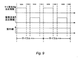
図9は、一実施形態の2つのサイクル910A及び910Bを示し、各サイクルの持続時間の間、紫外線が照射され続ける。各サイクルでは、ケイ素含有反応物質を流し(サイクル910Aではフェーズ920Aで、サイクル910Bではフェーズ920B)、必要に応じて、次にパージフェーズを実施し(サイクル910Aではフェーズ20Aで、サイクル910Bではフェーズ20B)、窒素含有反応物質を流し(サイクル910Aではフェーズ930Aで、サイクル910Bではフェーズ930B)、必要に応じて、次にパージフェーズを実施する(サイクル910Aではフェーズ30Aで、サイクル910Bではフェーズ30B)。一部の実施形態において、サイクル910A及び910Bの一部の期間で、たとえば、必要に応じて行われるパージフェーズが実施される場合にはその間、紫外線の照射を停止するようにしてもよい。
FIG. 9 illustrates two cycles 910A and 910B of one embodiment, where the ultraviolet light continues to be radiated for the duration of each cycle. In each cycle, a silicon-containing reactant is flowed (
図10は、一実施形態の2つのサイクル1010A及び1010Bを示し、紫外線照射で活性化された後に、窒素含有反応物質が反応チャンバに導入される。蒸着サイクル1010Aでは、ケイ素含有反応物質を流し(フェーズ1020A)、必要に応じて、次にパージフェーズ20Aを実施する。その後、紫外線で活性化された窒素含有反応物質をチャンバに流入させると(フェーズ1030A)、チャンバ内で、表面に結合されたケイ素含有反応物質と反応して、SiN層を形成する。必要に応じて、次にパージフェーズ30Aを実施して、サイクル1010Aを終了するようにしてもよい。蒸着サイクル1010Bは、フェーズ1020B及び1030B、並びに、必要に応じて実施されるパージフェーズ20B及び30Bを含む。
FIG. 10 illustrates two cycles 1010A and 1010B of one embodiment, where nitrogen-containing reactants are introduced into the reaction chamber after being activated with ultraviolet radiation. In the deposition cycle 1010A, a silicon-containing reactant is flowed (
図11及び図12は、ケイ素含有反応物質を流すことと、窒素含有反応物質を流すことと、紫外線に曝露することとを連続的に行う蒸着処理の3段階サイクルの例を示す。まず、図11は、蒸着サイクル1110Aを示し、このサイクルは、フェーズ1120Aでケイ素含有反応物質を流すことにより開始される。この後に、必要に応じて、パージ20Aが続く。次に、フェーズ1140Aで、紫外線源がオンにされて、少なくとも表面に結合されたケイ素含有反応物質が紫外線に曝露される。フェーズ1140Aの後にも、必要に応じてパージフェーズ40Aが続く。次に、フェーズ1130Aで、窒素含有反応物質を反応器に流入させて、活性化された表面結合ケイ素含有反応物質と反応させることにより、SiNが形成される。このサイクルは、このフェーズの後に終了するようにしてもよいし、必要に応じて実施されるパージフェーズ30Aの後に終了するようにしてもよい。追加のサイクルを実施して、所望の厚さのSiN膜を蒸着させるようにしてもよい。
FIG. 11 and FIG. 12 show an example of a three-stage cycle of a vapor deposition process in which flowing a silicon-containing reactant, flowing a nitrogen-containing reactant, and exposing to ultraviolet light are continuously performed. First, FIG. 11 shows a deposition cycle 1110A, which is initiated by flowing a silicon-containing reactant in
図12は、蒸着サイクル1210を示し、このサイクルは、フェーズ1220Aで、ケイ素含有反応物質を流すことにより開始され、必要に応じてこれにパージ20Aが続く。次に、フェーズ1230Aで、窒素含有反応物質を反応器に流入させ、必要に応じてパージ30Aがこれに続く。フェーズ1240Aで、これらの反応物質を紫外線に曝露させて、反応を活性化し、SiNを形成する。表面に結合されたケイ素含有反応物質及び窒素含有反応物質のいずれかまたは両方を活性化できる。一部の実施形態において、必要に応じて行われるパージ30Aを実施せずに、フェーズ1240Aの間に、気相の窒素含有反応物質が存在するようにしてもよい。紫外線照射後に、必要に応じてパージ40Aを実施して、SiN材料の固体層を残し、サイクル1210Aを終了する。必要に応じて、追加のサイクルを実施して、所望の厚さの膜を蒸着させるようにしてもよい。一部の実施形態において、紫外線曝露フェーズは、フェーズ1230Aの後に行うのに加えて、フェーズ1220Aの後でフェーズ1230の前(たとえば、図11のように)にも行うようにしてもよい。
FIG. 12 shows a deposition cycle 1210, which begins in
図13は、一実施形態における進行を時系列で示し、フェーズ1320Aでは、紫外線照射の下でケイ素含有反応物質と窒素含有反応物質とを共に流す。たとえば、ケイ素含有反応物質が紫外線透過性であり、窒素含有反応物質が活性化されるものでもよい。この場合には、ケイ素含有反応物質上でラジカルが生成されることによって蒸着される。フェーズ1320Aの後に、必要に応じてパージフェーズ20Aを行い、サイクル1310Aを終了するようにしてもよい。1つ又は複数の追加のサイクルを実施するようにしてもよい。
FIG. 13 shows the progression in one embodiment in chronological order, and in
反応物質:
上述したように、ケイ素含有反応物質の例としては、シラン、ハロシラン又はアミノシランが挙げられる。シランは、水素及び/又は炭素基を含有するが、ハロゲンを含有しない。シランの例としては、シラン(SiH4)と、ジシラン(Si2H6)と、メチルシラン、エチルシラン、イソプロピルシラン、t‐ブチルシラン、ジメチルシラン、ジエチルシラン、ジ‐t‐ブチルシラン、アリルシラン、sec−ブチルシラン、テキシルシラン、イソアミルシラン、t‐ブチルジシラン、ジ‐t‐ブチルジシラン等のオルガノシランと、が挙げられる。ハロシランは、少なくとも1つのハロゲン基を含有するものであって、水素及び/又は炭素基を含有するものでも含有しないものでもよい。ハロシランの例としては、ヨードシラン、ブロモシラン、クロロシラン及びフルオロシランが挙げられる。ハロシラン、特にフルオロシランは、ケイ素材料をエッチング可能な反応性ハロゲン化合物種を形成することができるが、本明細書に記載する特定の実施形態においては、プラズマ照射の際にケイ素含有反応物質が存在しない。クロロシランの具体例としては、テトラクロロシラン(SiCl4)、トリクロロシラン(HSiCl3)、ジクロロシラン(H2SiCl2)、モノクロロシラン(ClSiH3)、クロロアリルシラン、クロロメチルシラン、ジクロロメチルシラン、クロロジメチルシラン、クロロエチルシラン、t‐ブチルクロロシラン、ジ‐t‐ブチルクロロシラン、クロロイソプロピルシラン、クロロ‐sec‐ブチルシラン、t‐ブチルジメチルクロロシラン、テキシルジメチルクロロシラン等が挙げられる。アミノシランは、ケイ素原子に結合される少なくとも1つの窒素原子を含むものであって、水素、酸素、ハロゲン及び炭素を含有するものでもよい。アミノシランの例としては、モノアミノシラン、ジアミノシラン、トリアミノシラン及びテトラアミノシラン(それぞれH3Si(NH2)4、H2Si(NH2)2、HSi(NH2)3及びSi(NH2)4)とともに、t‐ブチルアミノシラン、メチルアミノシラン、tert‐ブチルシランアミン、ビス(ターシャルブチルアミノ)シラン(SiH2(NHC(CH3)3)2(BTBAS))、ビス(ジメチルアミノ)ジメチルシラン及びケイ素とアミノ基の両方を炭素で置換した他の同様の化合物、tert‐ブチルシリルカルバメート、SiH(CH3)−(N(CH3)2)2、SiHCl−(N(CH3)2)2、(Si(CH3)2NH)3等の置換モノアミノシラン、置換ジアミノシラン、置換トリアミノシラン及び置換テトラアミノシランが挙げられる。アミノシランの別の例としては、トリシリルアミン(N(SiH3))がある。様々な実施形態において、ケイ素含有反応物質は、紫外線透過性のあるものでもよいし、ないものでもよい。紫外線透過性のケイ素含有反応物質が用いられる場合には、たとえば、図5、6〜7及び9〜13に関して上述したように、紫外線照射によって活性化される窒素含有共反応物質が存在する際に照射されるように紫外線曝露のタイミングを調節する。
Reactant:
As noted above, examples of silicon-containing reactants include silane, halosilane, or aminosilane. Silane contains hydrogen and / or carbon groups but does not contain halogens. Examples of silanes include silane (SiH 4 ), disilane (Si 2 H 6 ), methyl silane, ethyl silane, isopropyl silane, t-butyl silane, dimethyl silane, diethyl silane, di-t-butyl silane, allyl silane, sec-butyl silane. And organosilanes such as texylsilane, isoamylsilane, t-butyldisilane, and di-t-butyldisilane. The halosilane contains at least one halogen group and may or may not contain hydrogen and / or carbon groups. Examples of halosilanes include iodosilane, bromosilane, chlorosilane, and fluorosilane. Halosilanes, particularly fluorosilanes, can form reactive halogen species that can etch silicon materials, but in certain embodiments described herein, silicon-containing reactants are present during plasma irradiation. do not do. Specific examples of chlorosilane include tetrachlorosilane (SiCl 4 ), trichlorosilane (HSiCl 3 ), dichlorosilane (H 2 SiCl 2 ), monochlorosilane (ClSiH 3 ), chloroallylsilane, chloromethylsilane, dichloromethylsilane, chlorodimethyl Examples include silane, chloroethylsilane, t-butylchlorosilane, di-t-butylchlorosilane, chloroisopropylsilane, chloro-sec-butylsilane, t-butyldimethylchlorosilane, and texyldimethylchlorosilane. Aminosilanes contain at least one nitrogen atom bonded to a silicon atom and may contain hydrogen, oxygen, halogen and carbon. Examples of aminosilanes include monoaminosilane, diaminosilane, triaminosilane and tetraaminosilane (H 3 Si (NH 2 ) 4 , H 2 Si (NH 2 ) 2 , HSi (NH 2 ) 3 and Si (NH 2 ) 4 respectively. ), T-butylaminosilane, methylaminosilane, tert-butylsilaneamine, bis (tertiarybutylamino) silane (SiH 2 (NHC (CH 3 ) 3 ) 2 (BTBAS)), bis (dimethylamino) dimethylsilane and Other similar compounds in which both silicon and amino groups are substituted with carbon, tert-butylsilyl carbamate, SiH (CH 3 ) — (N (CH 3 ) 2 ) 2 , SiHCl— (N (CH 3 ) 2 ) 2 , (Si (CH 3 ) 2 NH) 3 substituted monoaminosilane, substituted diaminosilane, substituted triaminosilane and the like Examples include substituted tetraaminosilane. Another example of aminosilane is trisilylamine (N (SiH 3 )). In various embodiments, the silicon-containing reactant may or may not be UV transmissive. When UV transmissive silicon-containing reactants are used, for example, when there is a nitrogen-containing co-reactant activated by UV irradiation, as described above with respect to FIGS. 5, 6-7, and 9-13. Adjust the timing of UV exposure so that it is irradiated.
任意の適当な窒素含有反応物質を用いることができる。一つの実施形態において、アンモニア、ヒドラジン、アミン及びこれらの混合物からなる群から、窒素含有反応物質が選択される。一部の実施形態において、窒素含有反応物質は、気相中で紫外線によって活性化することができる。例としては、NH3、NR3、NR2H及びNRH2、N2及びフォーミングガス(N2/H2)が挙げられる。 Any suitable nitrogen-containing reactant can be used. In one embodiment, the nitrogen-containing reactant is selected from the group consisting of ammonia, hydrazine, amine, and mixtures thereof. In some embodiments, the nitrogen-containing reactant can be activated by ultraviolet radiation in the gas phase. Examples include NH 3 , NR 3 , NR 2 H and NRH 2 , N 2 and forming gas (N 2 / H 2 ).
一つの実施形態において、窒素含有反応物質は、C1〜C10のアルキルアミンのいずれか又はC1〜C10のアルキルアミンの混合物を含む。一つの実施形態において、C1〜C10のアルキルアミンは、第一級アルキルアミン又は第二級アルキルアミンである。一つの実施形態において、C1〜C10のアルキルアミンは、第一級アルキルアミンである。一つの実施形態において、C1〜C10のアルキルアミンは、式Iに従うものである。 In one embodiment, the nitrogen-containing reactant comprises any of C1-C10 alkylamines or a mixture of C1-C10 alkylamines. In one embodiment, the C1-C10 alkylamine is a primary alkylamine or a secondary alkylamine. In one embodiment, the C1-C10 alkylamine is a primary alkylamine. In one embodiment, the C1-C10 alkylamine is according to Formula I.

ここで、R1、R2及びR3は、それぞれ独立であり、H又はC1〜C3のアルキルである。あるいは、R1、R2及びR3のうち2つは、それらが結合する炭素原子と共に、C3〜C7のシクロアルキルを形成し、R1,R2及びR3の残りの1つは、H又はC1〜C3のアルキルである。一つの実施形態において、C1〜C10のアルキルアミンは、その窒素に直接結合される第二炭素又は第三炭素を有する。一つの実施形態において、C1〜C10のアルキルアミンは、イソプロピルアミン、シクロプロピルアミン、sec−ブチルアミン、tert−ブチルアミン、シクロブチルアミン、イソアミルアミン、2−メチルブタン−2−アミン及びテキシルアミン(2,3−ジメチルブタン−2−アミン)からなる群から選択される。一つの実施形態において、式IのC1〜C10のアルキルアミンにおいて、R1、R2及びR3は、それぞれC1〜C3のアルキルである。一つの実施形態において、C1〜C10のアルキルアミンは、tert−ブチルアミン(TBA)である。TBAを用いることができる。 Wherein, R 1, R 2 and R 3 are each independently H or alkyl of C1 to C3. Alternatively, two of R 1 , R 2 and R 3 together with the carbon atom to which they are attached form a C3-C7 cycloalkyl and the remaining one of R1, R2 and R3 is H or C1- C3 alkyl. In one embodiment, the C1-C10 alkyl amine has a secondary or tertiary carbon bonded directly to its nitrogen. In one embodiment, the C1-C10 alkylamine is isopropylamine, cyclopropylamine, sec-butylamine, tert-butylamine, cyclobutylamine, isoamylamine, 2-methylbutan-2-amine and texylamine (2,3-dimethylamine). Butane-2-amine). In one embodiment, in the C1-C10 alkylamine of Formula I, R1, R2, and R3 are each C1-C3 alkyl. In one embodiment, the C1-C10 alkylamine is tert-butylamine (TBA). TBA can be used.
一部の実施形態において、生成されたSiN膜は、不要な炭素を含有する。このように膜内に炭素が存在する結果、漏電が生じる可能性があり、ある誘電体バリア用途で膜を使えなくする可能性がある。炭素の含量は変動するが、一部の実施形態においては、約10%(重量パーセント)の炭素含量では高すぎると考えられる。本明細書に記載する方法は、SiN膜内の不要な炭素に対処するものである。本明細書に記載する方法によって、炭素含量が2%未満の、一つの実施形態では炭素含量が1%未満の、別の実施形態では炭素含量が0.5%未満の、SiN膜を生成する。一部の実施形態において、炭素残量の削減は、FTIRスペクトルで容易に観測可能である。ただし、当業者に周知の他の分析手法を用いて、これらの範囲の炭素含量を測定するようにしてもよい。 In some embodiments, the generated SiN film contains unwanted carbon. As a result of the presence of carbon in the film, electrical leakage can occur, which can render the film unusable for certain dielectric barrier applications. The carbon content varies, but in some embodiments, a carbon content of about 10% (weight percent) is considered too high. The method described herein addresses unwanted carbon in the SiN film. The method described herein produces a SiN film having a carbon content of less than 2%, in one embodiment having a carbon content of less than 1%, and in another embodiment having a carbon content of less than 0.5%. . In some embodiments, the reduction in carbon balance can be easily observed in the FTIR spectrum. However, the carbon content in these ranges may be measured using other analytical techniques well known to those skilled in the art.
一部の実施形態において、窒素含有反応物質は、熱的に除去可能な基を有するものでもよい。熱的に除去可能な基は、約200℃から約550℃の間の温度で揮発性成分に分解される基である。たとえば、第二炭素基及び特定の第三炭素基は、この温度範囲で脱離反応を起こすものでもよい。特定の例において、t−ブチル基は、この温度範囲で分解されてイソブチレンを形成する。たとえば、t−ブチルアミンを加熱することにより、脱離反応を起こして、イソブチレンとアンモニアを形成する。別の例として、t−ブトキシカルボニル基(t−BOC)も、熱的に、たとえば、約150℃で分解し、イソブチレンと、二酸化炭素と、t−BOC基が結合されるラジカルと、を形成する。たとえば、t−ブチルカルバメートは、熱分解して、イソブチレンアンモニアと二酸化炭素とを形成する。 In some embodiments, the nitrogen-containing reactant may have a thermally removable group. Thermally removable groups are groups that decompose into volatile components at temperatures between about 200 ° C. and about 550 ° C. For example, the second carbon group and the specific third carbon group may cause an elimination reaction in this temperature range. In certain instances, t-butyl groups are decomposed at this temperature range to form isobutylene. For example, by heating t-butylamine, an elimination reaction is caused to form isobutylene and ammonia. As another example, a t-butoxycarbonyl group (t-BOC) is also thermally decomposed at, for example, about 150 ° C. to form isobutylene, carbon dioxide, and a radical to which the t-BOC group is bound. To do. For example, t-butyl carbamate thermally decomposes to form isobutylene ammonia and carbon dioxide.
約200℃〜約550℃に基板を加熱することにより、このような基を分解して、それに含有される炭素を放出させて、SiN膜の炭素含量を削減することができる。反応物質が基板上に吸着され、プラズマを用いて、反応物質がSiN材料に変換される。基板を加熱することにより、残った炭素基を除去することができる。蒸着工程全体にわたって加熱を行う、又は、周期的に加熱を行うことにより、熱的に除去可能な基を分解することができる。一つの実施形態において、約200℃〜約550℃に基板を加熱する。別の実施形態において、約350℃〜約550℃に基板を加熱する。また別の実施形態において、約450℃〜約550℃に基板を加熱する。さらに別の実施形態において、約450℃〜約500℃に基板を加熱する。一つの実施形態において、たとえばTBAを用いる場合には、約1秒間〜約30秒間、又は、約1秒間〜約20秒間、又は、約1秒間〜約10秒間、約450℃〜約500℃にSiN膜を加熱するようにしてもよい。ある温度閾値において特定の熱的に除去可能な基を分解することができるが、より高い温度にして、分解率を増大させる、及び/又は、焼きなましを行い、SiN膜の特性を向上させるようにしてもよい。 By heating the substrate to about 200 ° C. to about 550 ° C., the carbon content of the SiN film can be reduced by decomposing such groups and releasing the carbon contained therein. The reactant is adsorbed on the substrate, and the reactant is converted into a SiN material using plasma. The remaining carbon group can be removed by heating the substrate. The thermally removable group can be decomposed by heating throughout the deposition process or by heating periodically. In one embodiment, the substrate is heated to about 200 ° C to about 550 ° C. In another embodiment, the substrate is heated to about 350 ° C to about 550 ° C. In yet another embodiment, the substrate is heated to about 450 ° C to about 550 ° C. In yet another embodiment, the substrate is heated to about 450 ° C to about 500 ° C. In one embodiment, for example when using TBA, from about 1 second to about 30 seconds, or from about 1 second to about 20 seconds, or from about 1 second to about 10 seconds, from about 450 ° C. to about 500 ° C. The SiN film may be heated. Certain thermally removable groups can be decomposed at a certain temperature threshold, but higher temperatures can be used to increase the decomposition rate and / or anneal to improve the properties of the SiN film. May be.
上述したように、熱的に除去可能な基は、第二炭素又は第三炭素官能性を有するものでもよい。ケイ素含有反応物質と窒素含有反応物質のいずれか又は両方が、同一の又は異なる熱的に除去可能な基を備えるものでもよい。一つの実施形態において、熱的に除去可能な基は、式IIに従うものである。 As noted above, thermally removable groups may have secondary or tertiary carbon functionality. Either or both of the silicon-containing reactant and the nitrogen-containing reactant may comprise the same or different thermally removable groups. In one embodiment, the thermally removable group is according to Formula II.
ここで、R1、R2及びR3は、それぞれ独立であり、H又はC1〜C3のアルキルである。あるいは、R1、R2及びR3のうち2つは、それらが結合する炭素原子と共に、C3〜C7のシクロアルキルを形成し、R1,R2及びR3の残りの1つは、H又はC1〜C3のアルキルである。ここで、熱的に除去可能な各基は、窒素含有反応物質の一部の場合には、窒素含有反応物質の窒素又は酸素に結合し、ケイ素含有反応物質の一部の場合には、ケイ素含有反応物質のケイ素、窒素又は酸素に結合する。一つの実施形態において、R1、R2及びR3は、それぞれ独立であり、C1〜C3のアルキルである。一つの実施形態において、熱的に除去可能な基は、t−ブチル基である。 Wherein, R 1, R 2 and R 3 are each independently H or alkyl of C1 to C3. Alternatively, two of R 1 , R 2 and R 3 together with the carbon atom to which they are attached form a C3-C7 cycloalkyl and the remaining one of R1, R2 and R3 is H or C1- C3 alkyl. Here, each thermally removable group is bonded to nitrogen or oxygen of the nitrogen-containing reactant in the case of a part of the nitrogen-containing reactant, and silicon in the case of a part of the silicon-containing reactant. Bonds to contained reactants silicon, nitrogen or oxygen. In one embodiment, R 1 , R 2 and R 3 are each independent and are C1-C3 alkyl. In one embodiment, the thermally removable group is a t-butyl group.
装置:
本発明の別の態様は、本明細書に記載する方法を実施するように構成される装置である。適切な装置は、本発明に従って、処理操作を実施するためのハードウェアと、処理操作を制御するための指示を有するシステム制御部と、を備える。
apparatus:
Another aspect of the invention is an apparatus configured to perform the methods described herein. A suitable apparatus comprises hardware for performing a processing operation and a system controller having instructions for controlling the processing operation in accordance with the present invention.
当然のことながら、上述した実施例の一つ又は複数において、任意の適当な処理ステーションを用いることができる。たとえば、図14は、CFD処理ステーション2300の概略を示す図である。分かりやすくするために、CFD処理ステーション2300を、低圧環境を維持する処理チャンバ本体2302を備えるスタンドアロン型の処理ステーションとして例示する。ただし、当然のことながら、共通の低圧処理ツール環境に、複数のCFD処理ステーション2300を備えるようにしてもよい。図14に示す実施形態では処理ステーションは一つであるが、当然のことながら、ある実施形態において、処理ツール内に複数の処理ステーションを備えるようにしてもよい。たとえば、図15は、マルチステーション型の処理ツール2400の実施形態を示す。さらに、当然のことながら、ある実施形態において、以下に詳細に説明するものを含めてCFD処理ステーション2300の1つ又は複数のハードウェアパラメータを、1つ又は複数のコンピュータ制御部によってプログラム的に調整するようにしてもよい。
Of course, any suitable processing station may be used in one or more of the embodiments described above. For example, FIG. 14 is a diagram showing an outline of the
CFD処理ステーション2300は、処理ガスを分配シャワーヘッド2306に供給するための反応物質供給システム2301と流体連結される。反応物質供給システム2301は、処理ガスを混合して、及び/又は、処理ガスを調整して、シャワーヘッド2306に供給するための混合容器2304を備える。一つ又は複数の混合容器入口弁2320により、混合容器2304への処理ガスの導入を制御するようにしてもよい。
The
一部の反応物質を、次の処理ステーションへの供給時に気化するまで、液体の形態で保存するようにしてもよい。たとえば、図14の装置は、混合容器2304に供給するべき液体反応物質を気化する蒸発ポイント2303を備える。一部の実施形態において、蒸発ポイント2303は、加熱気化器でもよい。このような気化器で生成される反応物質の飽和蒸気を下流側の供給配管で濃縮するようにしてもよい。濃縮された反応物質がこれと混合できないガスに曝露されると、微粒子が形成される可能性がある。このような微粒子は、配管を詰まらせて、弁操作を妨げ、基板を汚染する等の可能性がある。このような問題に対処する一部のアプローチは、供給配管をスイープする、及び/又は、供給配管を減圧にすることによって、残留する反応物質を除去するものである。ただし、供給配管をスイープすることにより、処理ステーションのサイクルタイムが増大し、処理ステーションのスループットを低下させる。したがって、一部の実施形態において、蒸発ポイント2303の下流側の供給配管をヒートトレースする。いくつかの例では、混合容器2304もヒートトレースする。非限定的な一例として、蒸発ポイント2303の下流側の配管は、混合容器2304において約100℃から約150℃に広がる温度上昇プロファイルを有する。
Some reactants may be stored in liquid form until they are vaporized upon delivery to the next processing station. For example, the apparatus of FIG. 14 includes an
一部の実施形態において、液体反応物質を液体注入器で気化する。たとえば、液体注入器は、混合容器の上流側のキャリアガス流内に液体反応物質をパルス状に注入するものでもよい。一つの実施形態において、液体注入器により高圧側から低圧側に液体をフラッシングさせることによって、反応物質を気化させる。別の実施形態において、液体注入器により液体を噴霧して分散微液滴を形成し、次にこの分散微液滴を加熱供給配管で気化する。当然のことながら、小さな液滴は大きな液滴よりも速く気化できるため、液体注入と気化完了との間の遅れを抑制できる。気化が速く行われることにより、蒸発ポイント2303から下流側の配管の長さを短くすることができる。一つの実施形態において、液体注入器は、混合容器2304に直接取り付けられる。別の実施形態において、液体注入器は、シャワーヘッド2306に直接取り付けられる。
In some embodiments, the liquid reactant is vaporized with a liquid injector. For example, the liquid injector may inject the liquid reactant in pulses into a carrier gas stream upstream of the mixing vessel. In one embodiment, the reactants are vaporized by flushing the liquid from the high pressure side to the low pressure side with a liquid injector. In another embodiment, the liquid is sprayed by a liquid injector to form dispersed microdroplets, which are then vaporized in a heated supply line. Naturally, small droplets can be vaporized faster than large droplets, so that the delay between liquid injection and vaporization completion can be suppressed. By performing the vaporization quickly, the length of the pipe on the downstream side from the
一部の実施形態において、蒸発ポイント2303の上流側に液体流量制御装置を設置して、気化されて、処理ステーション1300に供給される液体の質量流を制御する。たとえば、液体流量制御装置(LFC:liquid flow controller)は、LFCの下流側に配置される熱質量流量計(MFM:mass flow meter)を備える。MFMと電気的に通信する比例・積分・微分(PID:proportional-integral-derivative)制御器によって与えられるフィードバック制御信号に応じて、LFCのプランジャー値が調整される。ただし、フィードバック制御を利用して液体流量を安定化させるためには、1秒以上の時間がかかることがある。これにより、液体反応物質を添加する時間が延びる可能性がある。したがって、一部の実施形態において、フィードバック制御モードと直接制御モードとの間でLFCを動的に切り替える。一部の実施形態において、LFCとPID制御器の検知管の動作を停止させることによって、フィードバック制御モードから直接制御モードに、LFCを動的に切り替える。
In some embodiments, a liquid flow controller is installed upstream of the
シャワーヘッド2306は、基板2312に向かって処理ガスを分配する。図14に示す実施形態において、基板2312は、シャワーヘッド2306の下方に配置され、図示されるように台座1308上に載置される。当然のことながら、シャワーヘッド2306は、任意の適当な形状でよく、処理ガスを基板2312に分配する任意の数および配置のポートを備えるものでもよい。
The
一部の実施形態において、シャワーヘッド2306の下方に微小容積2307が存在する。処理ステーションの全容積というよりも微小容積内でCFD処理を行うことによって、反応物質の曝露及びスイープ時間を減少させる、CFD処理条件(たとえば、圧力や温度等)を変更する時間を削減する、処理ステーションのロボティクスの処理ガスへの曝露を抑制する、等が可能になる。微小容積の大きさの例としては、以下に限定されるものではないが、0.1リットル〜2リットルの間の容積が挙げられる。
In some embodiments, there is a
一部の実施形態において、台座2308を上昇または降下させることによって、基板2312を微小容積2307に曝露させる、及び/又は、微小容積2307の体積を変化させるようにしてもよい。たとえば、基板移動フェーズにおいて、台座2308を降下させて、基板2312を台座2308上に載置することができる。CFD処理フェーズの際に、台座2308を上昇させて、基板2312を微小容積2307内に位置させる。一部の実施形態において、微小容積2307は、基板2312と台座2308の一部とを完全に内包し、CFD処理の間、フローインピーダンスの高い領域を形成する。
In some embodiments, the
CFD処理の一部の期間中に、必要に応じて、台座2308を降下及び/又は上昇させて、微小容積2307内における処理圧力や反応物質濃度等を変更するようにしてもよい。CFD処理の間、処理チャンバ本体2302を基底圧力に維持する一つの実施形態において、台座2308を降下させることによって、微小容積2307を減圧することができる。処理チャンバの容積に対する微小容積の割合の例としては、以下に限定されるものではないが、1:500〜1:10の間の容積比が挙げられる。当然のことながら、一部の実施形態において、適当なコンピュータ制御部を用いて、台座の高さをプログラム的に調整することができる。
During a part of the CFD processing, the
別の実施形態において、台座2308の高さを調整することによって、CFD処理におけるプラズマ活性化及び/又は処理サイクルの間のプラズマ密度を変えることができる。CFD処理フェーズが終わると、次の基板移動フェーズの間、台座2308を降下させて、台座2308から基板2312を取り外すことができるようにする。
In another embodiment, adjusting the height of the
本明細書では、微小容積を変化させる例として、高さ調整可能な台座に言及したが、当然のことながら、一部の実施形態において、台座2308に対してシャワーヘッド2306の位置を調整して、微小容積2307の体積を変更するようにしてもよい。さらに、当然のことながら、台座2308及び/又はシャワーヘッド2306の鉛直方向の位置を任意の適当な機構で変えるようにしてもよい。当業者には当然のことながら、このような機構としては、たとえば、油圧、空気圧、バネ機構、ソレノイド等が含まれる。一部の実施形態において、台座2308は、たとえば、基板表面に垂直な軸に沿って回転機構を備え、基板2312の方向を回転させるようにしてもよい。当然のことながら、一部の実施形態において、このように例示される調整のうち1つ又は複数を、1つ又は複数の適当なコンピュータ制御部によって、プログラム的に実行するようにしてもよい。
In this specification, the height-adjustable pedestal is referred to as an example of changing the minute volume. However, in some embodiments, the position of the
図14に示す実施形態に戻り、シャワーヘッド2306と台座1308とは、RF電力供給部2314及び照合ネットワーク2316と電気的に通信して、プラズマに電力を供給する。一部の実施形態において、処理ステーションの圧力、ガス濃度、RF源の電力、RF源の周波数及びプラズマ出力パルスのタイミングのうち1つ又は複数を制御することにより、プラズマエネルギーが制御される。たとえば、RF電力供給部2314及び照合ネットワーク2316を任意の適当な電力で作動させて、所望のラジカル種の組成を有するプラズマを形成させることができる。適当な電力の例としては、以下に限定されるものではないが、100W〜5000Wの電力が挙げられる。同様に、RF電力供給部2314は、任意の適当な周波数のRF電力を供給することができる。一部の実施形態において、RF電力供給部2314は、互いに独立に高周波RF電源と低周波RF電源とを制御するように構成されるものでもよい。低周波RF周波数の例としては、以下に限定されるものではないが、50kHz〜500kHzの周波数が挙げられる。高周波RF周波数の例としては、以下に限定されるものではないが、1.8MHz〜2.45GHzの周波数が挙げられる。当然のことながら、任意の適当なパラメータを離散的に又は連続的に調節して、表面反応にプラズマエネルギーを供給するようにしてもよい。非限定的な一例において、プラズマ出力を断続的にパルス状に変化させ、連続的に電力供給されるプラズマと比べて、基板表面とのイオン衝撃を減少させることができる。
Returning to the embodiment shown in FIG. 14, the
一部の実施形態において、1つ又は複数のプラズマモニタによりin situ(その場)でプラズマをモニターする。一つの実施形態において、1つ又は複数の電圧、電流センサ(たとえば、VIプローブ)によって、プラズマ出力をモニターする。別の実施形態において、1つ又は複数の発光分光(OES)センサによって、プラズマ密度及び/又は処理ガス濃度を測定する。一部の実施形態において、このようなin situ(その場)プラズマモニタからの測定値に基づいて、1つ又は複数のプラズマパラメータをプログラム的に調整する。たとえば、OESセンサをフィードバックループで用いて、プラズマ出力をプログラム的に制御するようにしてもよい。当然のことながら、一部の実施形態において、他のモニタを用いて、プラズマ及び他の処理特性をモニターするようにしてもよい。このようなモニタとしては、以下に限定されるものではないが、赤外(IR)モニタ、音響モニタ及び圧力トランスデューサが挙げられる。 In some embodiments, the plasma is monitored in situ by one or more plasma monitors. In one embodiment, the plasma output is monitored by one or more voltage, current sensors (eg, VI probes). In another embodiment, plasma density and / or process gas concentration is measured by one or more emission spectroscopy (OES) sensors. In some embodiments, one or more plasma parameters are programmatically adjusted based on measurements from such in situ plasma monitors. For example, an OES sensor may be used in a feedback loop to control the plasma output programmatically. Of course, in some embodiments, other monitors may be used to monitor plasma and other processing characteristics. Such monitors include, but are not limited to, infrared (IR) monitors, acoustic monitors, and pressure transducers.
一部の実施形態において、入出力制御(IOC:input/output control)シーケンシング命令によりプラズマを制御する。たとえば、プラズマ処理フェーズのためのプラズマ条件を設定する命令を、CFD処理レシピの対応するプラズマ活性レシピフェーズに含むようにしてもよい。一部の実施形態において、処理レシピフェーズを順次配列させて、CFD処理フェーズのすべての命令が、処理フェーズと同時に実行されるようにしてもよい。当然のことながら、プラズマ生成の態様は、プラズマ処理フェーズを引き延ばす可能性がある、特徴的な過渡時間及び/又は安定化時間を有するものでもよい。言い換えれば、このような時間遅延は予測可能である。このような時間遅延には、所定の出力設定で、プラズマを照射する時間及びプラズマを安定化する時間が含まれるものでもよい。 In some embodiments, the plasma is controlled by input / output control (IOC) sequencing instructions. For example, an instruction to set plasma conditions for the plasma processing phase may be included in the corresponding plasma activation recipe phase of the CFD processing recipe. In some embodiments, the process recipe phases may be arranged sequentially so that all instructions in the CFD process phase are executed simultaneously with the process phase. Of course, aspects of plasma generation may have characteristic transient times and / or stabilization times that may prolong the plasma processing phase. In other words, such a time delay is predictable. Such time delay may include time for plasma irradiation and time for plasma stabilization at a predetermined output setting.
一部の実施形態において、ヒータ2310を用いて、台座2308の温度制御をするようにしてもよい。さらに、一部の実施形態において、バタフライ弁2318で、CFD処理ステーション2300の圧力制御を行うようにしてもよい。図14に示すように、バタフライ弁2318は、(図示しない)下流側真空ポンプによって与えられる真空をスロットル調整する。ただし、一部の実施形態において、CFD処理ステーション2300に導入される1つ又は複数のガスの流量を変化させることによって、処理ステーション2300の圧力制御を調節するようにしてもよい。
In some embodiments, the
上述したように、1つ又は複数の処理ステーションをマルチステーション型処理ツールに備えるようにしてもよい。図15は、搬入(インバウンド)ロードロック2402と搬出(アウトバウンド)ロードロック2404とを備えるマルチステーション型処理ツール2400の概略図を示す。搬入ロードロック2402と搬出ロードロック2404のいずれか片方又は両方が遠隔プラズマ源を備えるものでもよい。ロボット2406は、大気圧において、ポッド2408によって積載されたカセットから搬入ロードロック2402に、大気ポート2410を介して、ウエハを移動するように構成される。ロボット2406により搬入ロードロック2402内の台座2412上にウエハが置かれると、大気ポート2410が閉じて、ロードロックがポンプダウンされる。搬入ロードロック2402が遠隔プラズマ源を備える場合には、処理チャンバ2414に導入される前に、ロードロックにおいて、ウエハが遠隔プラズマ処理を受けるようにしてもよい。さらに、搬入ロードロック2402においてウエハも同様に加熱して、たとえば、水分と吸着されたガスとを除去するようにしてもよい。次に、処理チャンバ2414へのチャンバ搬送ポート2416が開き、(図示しない)他のロボットが、反応器内にウエハを入れて、処理を行う反応器の図示される第1のステーションの台座上にウエハを載置する。図15に示す実施形態はロードロックを備えているが、当然のことながら、一部の実施形態において、処理ステーション内に直接ウエハを入れるようにしてもよい。
As described above, one or more processing stations may be provided in a multi-station processing tool. FIG. 15 shows a schematic diagram of a
図15に示す実施形態において、図示される処理チャンバ2414は、1〜4の番号をふられた4つの処理ステーションを備える。各ステーションは、加熱台座(ステーション1では2418で示す)と、ガス管入口と、を備える。当然のことながら、一部の実施形態において、各処理ステーションは、異なる目的を持つものでもよいし、複数の目的を持つものでもよい。たとえば、一部の実施形態において、CFD処理モードとPECVD処理ぽーどとの間で処理ステーションを切り替え可能としてもよい。さらに、又は、代わりに、一部の実施形態において、処理チャンバ2414は、1対又は複数対のCFD及びPECVD処理ステーションの組み合わせを備えるものでもよい。またさらに、一部の実施形態において、処理チャンバ2414は、1つ又は複数の紫外線硬化ステーション又は遠隔プラズマ処理ステーションを備えるものでもよい。図示される処理チャンバ2414は4つのステーションを備えるが、当然のことながら、本発明に従う処理チャンバは、任意の適当な数のステーションを備えるものでもよい。たとえば、一部の実施形態において、処理チャンバは、5つ以上のステーションを備えるものでもよく、別の実施形態において、処理チャンバは、3つ以下のステーションを備えるものでもよい。
In the embodiment shown in FIG. 15, the illustrated
さらに、処理チャンバ2414内でウエハを移動させるウエハ取扱いシステム2490を図15に示す。一部の実施形態において、ウエハ取扱いシステム2490は、異なる処理ステーション間で、及び/又は、処理ステーションとロードロックとの間で、ウエハを移動させることができる。当然のことながら、任意の適当なウエハ取扱いシステムを用いることができる。非限定的な例として、ウエハ回転式コンベヤ及びウエハ取扱いロボットが挙げられる。さらに、処理ツール2400の処理条件とハードウェア状態とを制御するために用いられるシステム制御部2450を図15に示す。システム制御部2450は、1つ又は複数の記憶装置2456と、1つ又は複数の大容量記憶装置2454と、1つ又は複数のプロセッサ2452と、を備えるものでもよい。プロセッサ2452は、CPU又はコンピュータ、アナログ及び/又はデジタル入出力接続、ステッピングモータ制御ボード等を備えるものでもよい。
Further, a
一部の実施形態において、システム制御部2450は、処理ツール2400の動作のすべてを制御する。システム制御部2450は、大容量記憶装置2454に格納されて、記憶装置2456にロードされ、プロセッサ2452上で実行されるシステム制御ソフトウェア2458を実行する。システム制御ソフトウェア2458は、タイミング、ガス混合物、チャンバ及び/又はステーション圧力、チャンバ及び/又はステーション温度、ウエハ温度、目標出力レベル、RF出力レベル、基板台座、チャック及び/又はサセプタ位置、及び、処理ツール2400によって実行される特定処理用の他のパラメータを制御するための命令を備えるものでもよい。システム制御ソフトウェア2458は、任意の適当な構成を備えるものでもよい。たとえば、種々の処理ツールの処理を実行するために必要な処理ツールの構成要素の動作を制御するために、様々な処理ツール構成要素サブルーチン又は制御オブジェクトが書き込まれるようにしてもよい。システム制御ソフトウェア2458は、任意の適当なコンピュータ読み取り可能なプログラム言語によってコード化されるものでもよい。
In some embodiments, the
一部の実施形態において、システム制御ソフトウェア2458は、上述した様々なパラメータを制御するための入出力制御(IOC)シーケンシング命令を備えるものでもよい。たとえば、CFD処理の各フェーズは、システム制御部2450により実行される1つ又は複数の命令を備えるものでもよい。CFD処理フェーズのための処理条件を設定する命令が、対応するCFDレシピフェーズに含まれるようにしてもよい。一部の実施形態において、CFDレシピフェーズを順次配列して、CFD処理フェーズ用のすべての命令が処理フェーズと同時に実行されるようにしてもよい。
In some embodiments, the
一部の実施形態において、システム制御部2450と関係する大容量記憶装置2454及び/又は記憶装置2456上に格納される他のコンピュータソフトウェア及び/又はプログラムを用いるようにしてもよい。このためのプログラムまたはプログラム部分の例には、基板位置決めプログラム、処理ガス制御プログラム、圧力制御プログラム、ヒーター制御プログラム及びプラズマ制御プログラムが含まれる。
In some embodiments,
基板位置決めプログラムは、台座2418上に基板を載置して、基板と処理ツール2400の他の部分との間の間隔を制御するために用いられる処理ツール構成要素用のプログラムコードを備えるものでもよい。
The substrate positioning program may include program code for processing tool components used to place the substrate on the
処理ガス制御プログラムは、ガス組成と流量とを制御するためのコード、及び、必要に応じて、蒸着前に1つ又は複数の処理ステーションにガスを流入させて、処理ステーション内の圧力を安定化させるためのコードを備えるものでもよい。圧力制御プログラムは、たとえば、処理ステーションの排出システムにおけるスロットルバルブや処理ステーションに流入するガス流量等を調整することによって、処理ステーション内の圧力を制御するためのコードを備えるものでもよい。 The process gas control program stabilizes the pressure in the process station by supplying code to control the gas composition and flow rate and, if necessary, the gas into one or more process stations before deposition. It may be provided with a code for making it happen. The pressure control program may include a code for controlling the pressure in the processing station by adjusting, for example, a throttle valve in the exhaust system of the processing station, a gas flow rate flowing into the processing station, or the like.
ヒーター制御プログラムは、基板を加熱するために用いられる加熱装置に供給される電流を制御するためのコードを備えるものでもよい。あるいは、ヒーター制御プログラムは、基板への熱伝導ガス(たとえば、ヘリウム)の供給を制御するようにしてもよい。 The heater control program may include a code for controlling a current supplied to a heating device used for heating the substrate. Or you may make it a heater control program control supply of the heat conductive gas (for example, helium) to a board | substrate.
プラズマ制御プログラムは、1つ又は複数の処理ステーションにおいて処理電極に印加されるRF出力レベルを設定するためのコードを備えるものでもよい。 The plasma control program may comprise code for setting the RF power level applied to the processing electrode at one or more processing stations.
一部の実施形態において、システム制御部2450に関連するユーザインタフェースを備えるものでもよい。ユーザインタフェースは、ディスプレイスクリーン、装置及び/又は処理条件のグラフィックソフトウェア・ディスプレイ、並びに、ポインティングデバイス、キーボード、タッチスクリーン、マイク等のユーザ入力装置を備えるものでもよい。
In some embodiments, a user interface associated with the
一部の実施形態において、システム制御部2450により調節されるパラメータは、処理条件に関係するものでもよい。非限定的な例として、処理ガスの組成及び流量、温度、圧力、プラズマ条件(たとえば、RFバイアス電力レベル)、圧力、温度等が挙げられる。これらのパラメータは、ユーザインタフェースを用いて入力可能なレシピの形でユーザに提供されるものでもよい。
In some embodiments, the parameters adjusted by the
システム制御部2450のアナログ及び/又はデジタル入力接続によって、様々な処理ツールセンサから、処理をモニタリングするための信号を提供するようにしてもよい。処理を制御するための信号を、処理ツール2400のアナログ及びデジタル出力接続に出力するようにしてもよい。モニタリング可能な処理ツールセンサの非限定的な例として、質量流量制御装置、(圧力計等の)圧力センサ、熱電対等が挙げられる。これらのセンサから得られるデータと共に、適切にプログラミングされたフィードバック及び制御アルゴリズムを用いて、処理条件を維持するようにしてもよい。
The analog and / or digital input connections of the
システム制御部2450は、上述した蒸着処理を実現するためのプログラム命令を提供するものでもよい。プログラム命令は、直流電力レベル、RFバイアス電力レベル、圧力、温度等、種々の処理パラメータを制御するものでもよい。命令は、パラメータを制御して、本明細書に記載する様々な実施形態に従って積層膜のin situ(その場)蒸着の操作を行うようにしてもよい。
The
システム制御部は、一般的に、1つ又は複数の記憶装置と、命令を実行することによって、本発明に従う方法を装置が実施するように構成される1つ又は複数のプロセッサと、を備える。本発明に従う処理操作を制御するための命令を含むマシン読み取り可能な媒体をシステム制御部に連結させるようにしてもよい。 The system controller generally comprises one or more storage devices and one or more processors configured to execute the instructions so that the device performs the method according to the present invention. A machine readable medium containing instructions for controlling processing operations according to the present invention may be coupled to the system controller.
実施例:
本明細書に記載する実施形態に従う紫外線及び遠隔プラズマを用いる方法によって、ビス(ジメチルアミノ)ジメチルシラン及び窒素反応物質を反応させて、ケイ素含有膜を形成した。紫外線ランプをそれぞれ有する4つのステーションを備える紫外線硬化装置を用いた。処理シーケンスを以下に示す。
Example:
The silicon-containing film was formed by reacting bis (dimethylamino) dimethylsilane and nitrogen reactants by a method using ultraviolet light and remote plasma according to embodiments described herein. An ultraviolet curing device with four stations each having an ultraviolet lamp was used. The processing sequence is shown below.
紫外線ALD:ステーション1及び3(紫外線ランプはオフ)でビス(ジメチルアミノ)ジメチルシラン曝露、ステーション2及び4で紫外線を用いてNH3曝露。シーケンス:ビス(ジメチルアミノ)ジメチルシラン曝露→パージ→パージ→次のステーションへ→紫外線を用いてNH3曝露→パージ→次のステーションへ。ステーション1及び3において、一般的なビス(ジメチルアミノ)ジメチルシラン暴露時間は20秒で、キャリア(Ar)1slmに対する流量は2mL/分であった。ステーション1及び3において、ウエハの浸漬時間は60秒であった。膜は、SiNを含有すると共に、SiNCピークの幅から考えると、Cが存在する可能性が高い。有意な量のN−H及びSi−Hの両方が存在していた。
UV ALD: exposure to bis (dimethylamino) dimethylsilane at
遠隔プラズマALD:ステーション3及び4でビス(ジメチルアミノ)ジメチルシラン曝露、ステーション1及び2で遠隔プラズマを用いてNH3(+Ar)曝露。すべてのステーションで紫外線ランプはオフ。アストロン(20秒曝露)を用いて、遠隔で、1slmのNH3/5slmのArによりNHxラジカルを生成。シーケンス:ビス(ジメチルアミノ)ジメチルシラン曝露→パージ→2つのステーションへ→遠隔プラズマNH3→パージ→2つのステーションへ。ステーション3及び4におけるウエハの浸漬時間は60秒であった。膜は主にSiN膜であり、炭素を含有する場合もある。Si−H結合は存在しなかった。RP時間を(20秒から)5秒に短縮しても、膜の厚さや膜の品質に影響はなかった。
Remote plasma ALD: bis (dimethylamino) dimethylsilane exposure at
パターン形成方法/装置:
本明細書に記載する装置/プロセスを、たとえば、半導体デバイス、ディスプレイ、LED、太陽光発電パネル等の製作又は製造用のリソグラフパターン形成ツールまたはプロセスと共に用いるようにしてもよい。必ずではないが、一般的に、このようなツール/プロセスを、共有の製造施設で共に用いる又は実施するようにしてもよい。膜のリソグラフパターン形成は、通常、以下の工程の一部または全部を備える。多くの利用可能なツールを用いて、各工程を実行することができる。(1)スピン式(回転式)ツール又はスプレー式ツールを用いて、ワークピース、すなわち、基板上にフォトレジストを塗布する。(2)ホットプレート、炉又は紫外線硬化ツールを用いて、フォトレジストを硬化させる。(3)ウエハステッパ等のツールを用いて、フォトレジストに可視光、紫外線又はx線を照射する。(4)ウェットベンチ等のツールを用いて、レジストを現像して、選択的にレジストを除去することにより、パターン化する。(5)ドライエッチングツールまたはプラズマ支援エッチングツールを用いて、レジストパターンを下層の膜又はワークピースに転写する。(6)RF又はマイクロ波プラズマレジストストリッパ等のツールを用いて、レジストを除去する。一つの実施形態において、本明細書に記載する方法を用いて、SiN膜が形成される。たとえば、本明細書に記載する目的のうちの一つにSiN膜を用いる。さらに、方法は、上述した1つ又は複数の工程(1)〜(6)を含む。
Pattern forming method / apparatus:
The apparatus / process described herein may be used in conjunction with a lithographic patterning tool or process for making or manufacturing semiconductor devices, displays, LEDs, photovoltaic panels, and the like, for example. Generally, although not necessarily, such tools / processes may be used or implemented together in a shared manufacturing facility. Formation of a lithographic pattern of a film usually comprises a part or all of the following steps. Each process can be performed using a number of available tools. (1) A photoresist is applied on a workpiece, that is, a substrate, using a spin type (rotary type) tool or a spray type tool. (2) The photoresist is cured using a hot plate, a furnace or an ultraviolet curing tool. (3) Irradiate the photoresist with visible light, ultraviolet rays, or x-rays using a tool such as a wafer stepper. (4) Using a tool such as a wet bench, the resist is developed and patterned by selectively removing the resist. (5) Using a dry etching tool or a plasma assisted etching tool, transfer the resist pattern to the underlying film or workpiece. (6) The resist is removed using a tool such as an RF or microwave plasma resist stripper. In one embodiment, a SiN film is formed using the methods described herein. For example, a SiN film is used for one of the purposes described in this specification. Further, the method includes one or more steps (1) to (6) described above.
Claims (26)
各サイクルは、
(a)窒素含有反応物質の気相流に前記基板を曝露し、
(b)ケイ素含有反応物質の気相流に前記基板を曝露し、
(c)前記窒素含有反応物質の気相流に紫外線を照射するとともに、前記ケイ素含有反応物質の気相流には紫外線を照射しない
方法。 Providing a substrate in a reaction chamber and performing one or more deposition cycles to deposit a silicon-containing film, the method comprising:
Each cycle is
(A) exposing the substrate to a gas phase flow of a nitrogen-containing reactant;
(B) exposing the substrate to a gas phase flow of a silicon-containing reactant;
(C) A method of irradiating the vapor phase flow of the nitrogen-containing reactant with ultraviolet rays and not irradiating the vapor phase flow of the silicon-containing reactant with ultraviolet rays.
前記基板は、ケイ素含有前駆物質の気相流に曝露される間に、前記窒素含有反応物質の気相流に曝露される、方法。 The method of claim 1, comprising:
The method wherein the substrate is exposed to a gas phase flow of the nitrogen-containing reactant while being exposed to a gas phase flow of the silicon-containing precursor.
前記基板は、ケイ素含有前駆物質の気相流に曝露される間には、前記窒素含有反応物質の気相流に曝露されない、方法。 The method of claim 1, comprising:
The method wherein the substrate is not exposed to the gas phase flow of the nitrogen-containing reactant while being exposed to the gas phase flow of the silicon-containing precursor.
前記反応チャンバ内で、前記窒素含有反応物質の気相流に紫外線が照射される、方法。 A method according to any one of claims 1 to 3, comprising
In the reaction chamber, the vapor stream of the nitrogen-containing reactant is irradiated with ultraviolet light.
前記チャンバの上流で、前記窒素含有反応物質の気相流に紫外線が照射される、方法。 A method according to any one of claims 1 to 3, comprising
The method wherein the vapor phase flow of the nitrogen-containing reactant is irradiated with ultraviolet light upstream of the chamber.
前記ケイ素含有反応物質は、シラン、ハロシラン、アミノシラン及びこれらの混合物からなる群から選択される、方法。 A method according to any one of claims 1 to 5, comprising
The method wherein the silicon-containing reactant is selected from the group consisting of silane, halosilane, aminosilane, and mixtures thereof.
前記ケイ素含有反応物質は、ケイ素及びアミノ基の部位に炭素含有置換基を有するアミノシランである、方法。 The method of claim 6, comprising:
The method, wherein the silicon-containing reactant is an aminosilane having a carbon-containing substituent at the silicon and amino group sites.
前記窒素含有反応物質は、アンモニア、ヒドラジン、アミン及びこれらの混合物からなる群から選択される、方法。 A method according to any one of claims 1 to 7, comprising
The method wherein the nitrogen-containing reactant is selected from the group consisting of ammonia, hydrazine, amine, and mixtures thereof.
前記ケイ素含有膜は、SiN、SiCN、SiON又はSiONCからなる群から選択される、方法。 A method according to any one of claims 1 to 8, comprising
The method wherein the silicon-containing film is selected from the group consisting of SiN, SiCN, SiON, or SiONC.
前記ケイ素含有膜はSiCNである、方法。 The method of claim 9, comprising:
The method wherein the silicon-containing film is SiCN.
各サイクルでは、
(a)遠隔プラズマ源を用いて、窒素含有反応物質の気相流を活性化し、
(b)前記活性化された窒素含有反応物質に前記基板を曝露し、
(c)ケイ素含有反応物質の気相流に前記基板を曝露する
方法。 Providing a substrate in a reaction chamber and performing one or more deposition cycles to deposit a silicon-containing film, the method comprising:
In each cycle,
(A) using a remote plasma source to activate the gas phase flow of the nitrogen-containing reactant;
(B) exposing the substrate to the activated nitrogen-containing reactant;
(C) exposing the substrate to a gas phase flow of a silicon-containing reactant;
前記基板は、ケイ素含有前駆物質の気相流に曝露される間に、前記窒素含有反応物質の気相流に曝露される、方法。 The method of claim 11, comprising:
The method wherein the substrate is exposed to a gas phase flow of the nitrogen-containing reactant while being exposed to a gas phase flow of the silicon-containing precursor.
前記基板は、ケイ素含有前駆物質の気相流に曝露される間には、前記窒素含有反応物質の気相流に曝露されない、方法。 The method of claim 11, comprising:
The method wherein the substrate is not exposed to the gas phase flow of the nitrogen-containing reactant while being exposed to the gas phase flow of the silicon-containing precursor.
前記ケイ素含有反応物質は、シラン、ハロシラン、アミノシラン及びこれらの混合物からなる群から選択される、方法。 A method according to any one of claims 11 to 13, comprising
The method wherein the silicon-containing reactant is selected from the group consisting of silane, halosilane, aminosilane, and mixtures thereof.
前記ケイ素含有反応物質は、ケイ素及びアミノ基の部位に炭素含有置換基を有するアミノシランである、方法。 15. A method according to claim 14, comprising
The method, wherein the silicon-containing reactant is an aminosilane having a carbon-containing substituent at the silicon and amino group sites.
前記窒素含有反応物質は、アンモニア、ヒドラジン、アミン及びこれらの混合物からなる群から選択される、方法。 A method according to any one of claims 11 to 15, comprising
The method wherein the nitrogen-containing reactant is selected from the group consisting of ammonia, hydrazine, amine, and mixtures thereof.
前記ケイ素含有膜は、SiN、SiCN、SiON又はSiONCからなる群から選択される、方法。 A method according to any one of claims 11 to 16, comprising
The method wherein the silicon-containing film is selected from the group consisting of SiN, SiCN, SiON, or SiONC.
前記ケイ素含有膜はSiCNである、方法。 A method according to any one of claims 11 to 17, comprising
The method wherein the silicon-containing film is SiCN.
(a)反応チャンバと、
(b)紫外線源と、
(c)反応物質入口と、
(d)前記反応チャンバ内に窒素含有反応物質の気相流を流入させる命令と、前記反応チャンバ内にケイ素含有反応物質の気相流を流入させる命令と、前記窒素含有反応物質の気相流に紫外線を照射するとともに、前記ケイ素含有反応物質の気相流には紫外線を照射しない命令と、を有する制御部と
を備える装置。 An apparatus for depositing a silicon nitride film on a semiconductor wafer,
(A) a reaction chamber;
(B) an ultraviolet light source;
(C) a reactant inlet;
(D) a command for flowing a vapor phase flow of nitrogen-containing reactant into the reaction chamber; a command for flowing a vapor phase flow of silicon-containing reactant into the reaction chamber; and a vapor phase flow of the nitrogen-containing reactant. And a control unit having a command to irradiate UV to the vapor phase flow of the silicon-containing reactant.
前記反応チャンバ内で、前記窒素含有反応物質の気相流に紫外線が照射される、装置。 The apparatus of claim 19, comprising:
An apparatus in which the vapor phase flow of the nitrogen-containing reactant is irradiated with ultraviolet light in the reaction chamber.
前記チャンバの上流で、前記窒素含有反応物質の気相流に紫外線が照射される、装置。 The apparatus of claim 19, comprising:
An apparatus wherein the vapor phase flow of the nitrogen-containing reactant is irradiated with ultraviolet light upstream of the chamber.
ケイ素含有前駆物質の気相流が流れる間に、前記窒素含有反応物質の気相流が流される、装置。 The apparatus according to any one of claims 19 to 21, comprising:
An apparatus wherein a vapor phase stream of the nitrogen-containing reactant is flowed while a vapor phase stream of a silicon-containing precursor flows.
ケイ素含有前駆物質の気相流が流れる間には、前記窒素含有反応物質の気相流が流れない、装置。 The apparatus according to any one of claims 19 to 21, comprising:
The apparatus wherein the vapor phase flow of the nitrogen-containing reactant does not flow while the vapor phase flow of the silicon-containing precursor flows.
(a)反応チャンバと、
(b)前記反応チャンバに対して遠隔のプラズマ源と、
(c)反応物質入口と、
(d)前記遠隔プラズマチャンバ内に窒素含有反応物質の気相流を流入させる命令と、前記遠隔プラズマ発生装置から前記反応チャンバ内に活性化窒素含有種を流入させる命令と、前記反応チャンバ内にケイ素含有反応物質の気相流を流入させる命令と、を有する制御部と
を備える装置。 An apparatus for depositing a silicon nitride film on a semiconductor wafer,
(A) a reaction chamber;
(B) a plasma source remote to the reaction chamber;
(C) a reactant inlet;
(D) a command to flow a vapor phase flow of nitrogen-containing reactant into the remote plasma chamber, a command to flow activated nitrogen-containing species from the remote plasma generator into the reaction chamber, and into the reaction chamber A control unit having instructions for injecting a gas phase flow of the silicon-containing reactant.
ケイ素含有前駆物質の気相流が流れる間に、前記窒素含有反応物質の気相流が流される、装置。 25. The apparatus of claim 24, comprising:
An apparatus wherein a vapor phase stream of the nitrogen-containing reactant is flowed while a vapor phase stream of a silicon-containing precursor flows.
ケイ素含有前駆物質の気相流が流れる間には、前記窒素含有反応物質の気相流が流れない、装置。 26. The method of claim 25, comprising:
The apparatus wherein the vapor phase flow of the nitrogen-containing reactant does not flow while the vapor phase flow of the silicon-containing precursor flows.
Applications Claiming Priority (5)
| Application Number | Priority Date | Filing Date | Title |
|---|---|---|---|
| US201261591230P | 2012-01-26 | 2012-01-26 | |
| US61/591,230 | 2012-01-26 | ||
| US13/472,282 | 2012-05-15 | ||
| US13/472,282 US8647993B2 (en) | 2011-04-11 | 2012-05-15 | Methods for UV-assisted conformal film deposition |
| PCT/US2013/022977 WO2013112727A1 (en) | 2012-01-26 | 2013-01-24 | Methods for uv-assisted conformal film deposition |
Publications (2)
| Publication Number | Publication Date |
|---|---|
| JP2015510263A true JP2015510263A (en) | 2015-04-02 |
| JP2015510263A5 JP2015510263A5 (en) | 2016-03-03 |
Family
ID=48870585
Family Applications (1)
| Application Number | Title | Priority Date | Filing Date |
|---|---|---|---|
| JP2014554825A Pending JP2015510263A (en) | 2012-01-26 | 2013-01-24 | Conformal film deposition using ultraviolet light |
Country Status (7)
| Country | Link |
|---|---|
| US (1) | US8647993B2 (en) |
| JP (1) | JP2015510263A (en) |
| KR (1) | KR20130086989A (en) |
| CN (1) | CN104081505A (en) |
| SG (1) | SG11201404315RA (en) |
| TW (1) | TW201349346A (en) |
| WO (1) | WO2013112727A1 (en) |
Cited By (11)
| Publication number | Priority date | Publication date | Assignee | Title |
|---|---|---|---|---|
| KR20160130152A (en) * | 2015-05-01 | 2016-11-10 | 도쿄엘렉트론가부시키가이샤 | Film forming method and film forming apparatus |
| JP2017028171A (en) * | 2015-07-24 | 2017-02-02 | 株式会社日立国際電気 | Semiconductor device manufacturing method, substrate processing apparatus and program |
| WO2017078082A1 (en) * | 2015-11-04 | 2017-05-11 | 国立研究開発法人産業技術総合研究所 | Production method and production device for nitrogen compound |
| JP2018137356A (en) * | 2017-02-22 | 2018-08-30 | 株式会社日立国際電気 | Semiconductor device manufacturing method, substrate processing apparatus and program |
| JP2020511797A (en) * | 2017-03-15 | 2020-04-16 | バーサム マテリアルズ ユーエス,リミティド ライアビリティ カンパニー | Novel formulations for the deposition of silicon-doped hafnium oxide as a ferroelectric material |
| JP2020065087A (en) * | 2015-11-12 | 2020-04-23 | エーエスエム アイピー ホールディング ビー.ブイ. | Formation of SiOCN thin film |
| WO2020213454A1 (en) * | 2019-04-16 | 2020-10-22 | 東京エレクトロン株式会社 | Film formation method and film formation device |
| JP2021511672A (en) * | 2018-01-26 | 2021-05-06 | アプライド マテリアルズ インコーポレイテッドApplied Materials,Incorporated | Treatment method for thin films of silicon nitride |
| WO2021100560A1 (en) * | 2019-11-21 | 2021-05-27 | 東京エレクトロン株式会社 | Substrate processing method and substrate processing device |
| WO2021100594A1 (en) * | 2019-11-19 | 2021-05-27 | 東京エレクトロン株式会社 | Substrate treatment method and substrate treatment device |
| JP7436982B2 (en) | 2019-03-06 | 2024-02-22 | 国立大学法人東北大学 | Silicon nitride film manufacturing method |
Families Citing this family (312)
| Publication number | Priority date | Publication date | Assignee | Title |
|---|---|---|---|---|
| US9394608B2 (en) | 2009-04-06 | 2016-07-19 | Asm America, Inc. | Semiconductor processing reactor and components thereof |
| US8802201B2 (en) | 2009-08-14 | 2014-08-12 | Asm America, Inc. | Systems and methods for thin-film deposition of metal oxides using excited nitrogen-oxygen species |
| US9892917B2 (en) | 2010-04-15 | 2018-02-13 | Lam Research Corporation | Plasma assisted atomic layer deposition of multi-layer films for patterning applications |
| US8956983B2 (en) | 2010-04-15 | 2015-02-17 | Novellus Systems, Inc. | Conformal doping via plasma activated atomic layer deposition and conformal film deposition |
| US9076646B2 (en) | 2010-04-15 | 2015-07-07 | Lam Research Corporation | Plasma enhanced atomic layer deposition with pulsed plasma exposure |
| US8637411B2 (en) | 2010-04-15 | 2014-01-28 | Novellus Systems, Inc. | Plasma activated conformal dielectric film deposition |
| US9997357B2 (en) | 2010-04-15 | 2018-06-12 | Lam Research Corporation | Capped ALD films for doping fin-shaped channel regions of 3-D IC transistors |
| US9390909B2 (en) | 2013-11-07 | 2016-07-12 | Novellus Systems, Inc. | Soft landing nanolaminates for advanced patterning |
| US9373500B2 (en) | 2014-02-21 | 2016-06-21 | Lam Research Corporation | Plasma assisted atomic layer deposition titanium oxide for conformal encapsulation and gapfill applications |
| US9611544B2 (en) | 2010-04-15 | 2017-04-04 | Novellus Systems, Inc. | Plasma activated conformal dielectric film deposition |
| US9257274B2 (en) | 2010-04-15 | 2016-02-09 | Lam Research Corporation | Gapfill of variable aspect ratio features with a composite PEALD and PECVD method |
| US8728956B2 (en) | 2010-04-15 | 2014-05-20 | Novellus Systems, Inc. | Plasma activated conformal film deposition |
| US9685320B2 (en) | 2010-09-23 | 2017-06-20 | Lam Research Corporation | Methods for depositing silicon oxide |
| US8647993B2 (en) | 2011-04-11 | 2014-02-11 | Novellus Systems, Inc. | Methods for UV-assisted conformal film deposition |
| US9312155B2 (en) | 2011-06-06 | 2016-04-12 | Asm Japan K.K. | High-throughput semiconductor-processing apparatus equipped with multiple dual-chamber modules |
| US10854498B2 (en) | 2011-07-15 | 2020-12-01 | Asm Ip Holding B.V. | Wafer-supporting device and method for producing same |
| US20130023129A1 (en) | 2011-07-20 | 2013-01-24 | Asm America, Inc. | Pressure transmitter for a semiconductor processing environment |
| US9017481B1 (en) | 2011-10-28 | 2015-04-28 | Asm America, Inc. | Process feed management for semiconductor substrate processing |
| JP6039996B2 (en) | 2011-12-09 | 2016-12-07 | 株式会社日立国際電気 | Semiconductor device manufacturing method, substrate processing method, substrate processing apparatus, and program |
| JP6049395B2 (en) * | 2011-12-09 | 2016-12-21 | 株式会社日立国際電気 | Semiconductor device manufacturing method, substrate processing method, substrate processing apparatus, and program |
| US8592328B2 (en) | 2012-01-20 | 2013-11-26 | Novellus Systems, Inc. | Method for depositing a chlorine-free conformal sin film |
| JP6041527B2 (en) * | 2012-05-16 | 2016-12-07 | キヤノン株式会社 | Liquid discharge head |
| JP6101467B2 (en) * | 2012-10-04 | 2017-03-22 | 東京エレクトロン株式会社 | Film forming method and film forming apparatus |
| US10714315B2 (en) | 2012-10-12 | 2020-07-14 | Asm Ip Holdings B.V. | Semiconductor reaction chamber showerhead |
| KR102207992B1 (en) | 2012-10-23 | 2021-01-26 | 램 리써치 코포레이션 | Sub-saturated atomic layer deposition and conformal film deposition |
| SG2013083654A (en) | 2012-11-08 | 2014-06-27 | Novellus Systems Inc | Methods for depositing films on sensitive substrates |
| SG2013083241A (en) | 2012-11-08 | 2014-06-27 | Novellus Systems Inc | Conformal film deposition for gapfill |
| US20140242811A1 (en) * | 2013-02-27 | 2014-08-28 | United Microelectronics Corp. | Atomic layer deposition method |
| US20140273524A1 (en) * | 2013-03-12 | 2014-09-18 | Victor Nguyen | Plasma Doping Of Silicon-Containing Films |
| US20140273526A1 (en) * | 2013-03-12 | 2014-09-18 | David Thompson | Atomic Layer Deposition Of Films Comprising Si(C)N Using Hydrazine, Azide And/Or Silyl Amine Derivatives |
| TW201522696A (en) * | 2013-11-01 | 2015-06-16 | Applied Materials Inc | Low temperature silicon nitride films using remote plasma CVD technology |
| US20150140833A1 (en) * | 2013-11-18 | 2015-05-21 | Applied Materials, Inc. | Method of depositing a low-temperature, no-damage hdp sic-like film with high wet etch resistance |
| US9214334B2 (en) | 2014-02-18 | 2015-12-15 | Lam Research Corporation | High growth rate process for conformal aluminum nitride |
| US10683571B2 (en) | 2014-02-25 | 2020-06-16 | Asm Ip Holding B.V. | Gas supply manifold and method of supplying gases to chamber using same |
| US10167557B2 (en) | 2014-03-18 | 2019-01-01 | Asm Ip Holding B.V. | Gas distribution system, reactor including the system, and methods of using the same |
| US11015245B2 (en) | 2014-03-19 | 2021-05-25 | Asm Ip Holding B.V. | Gas-phase reactor and system having exhaust plenum and components thereof |
| US9797042B2 (en) * | 2014-05-15 | 2017-10-24 | Lam Research Corporation | Single ALD cycle thickness control in multi-station substrate deposition systems |
| TW201610204A (en) * | 2014-07-26 | 2016-03-16 | 應用材料股份有限公司 | Low temperature molecular layer deposition of SiCON |
| US10858737B2 (en) | 2014-07-28 | 2020-12-08 | Asm Ip Holding B.V. | Showerhead assembly and components thereof |
| US9548188B2 (en) | 2014-07-30 | 2017-01-17 | Lam Research Corporation | Method of conditioning vacuum chamber of semiconductor substrate processing apparatus |
| US9564286B2 (en) * | 2014-08-14 | 2017-02-07 | Samsung Electronics Co., Ltd. | Method of forming thin film of semiconductor device |
| US9478438B2 (en) | 2014-08-20 | 2016-10-25 | Lam Research Corporation | Method and apparatus to deposit pure titanium thin film at low temperature using titanium tetraiodide precursor |
| US9478411B2 (en) | 2014-08-20 | 2016-10-25 | Lam Research Corporation | Method to tune TiOx stoichiometry using atomic layer deposited Ti film to minimize contact resistance for TiOx/Ti based MIS contact scheme for CMOS |
| US9890456B2 (en) | 2014-08-21 | 2018-02-13 | Asm Ip Holding B.V. | Method and system for in situ formation of gas-phase compounds |
| US9580801B2 (en) * | 2014-09-04 | 2017-02-28 | Applied Materials, Inc. | Enhancing electrical property and UV compatibility of ultrathin blok barrier film |
| US10941490B2 (en) | 2014-10-07 | 2021-03-09 | Asm Ip Holding B.V. | Multiple temperature range susceptor, assembly, reactor and system including the susceptor, and methods of using the same |
| US9657845B2 (en) | 2014-10-07 | 2017-05-23 | Asm Ip Holding B.V. | Variable conductance gas distribution apparatus and method |
| US9564312B2 (en) | 2014-11-24 | 2017-02-07 | Lam Research Corporation | Selective inhibition in atomic layer deposition of silicon-containing films |
| FI126970B (en) | 2014-12-22 | 2017-08-31 | Picosun Oy | Atomic deposit where the first and second starting species are present at the same time |
| US9490116B2 (en) * | 2015-01-09 | 2016-11-08 | Applied Materials, Inc. | Gate stack materials for semiconductor applications for lithographic overlay improvement |
| US10276355B2 (en) | 2015-03-12 | 2019-04-30 | Asm Ip Holding B.V. | Multi-zone reactor, system including the reactor, and method of using the same |
| US10566187B2 (en) | 2015-03-20 | 2020-02-18 | Lam Research Corporation | Ultrathin atomic layer deposition film accuracy thickness control |
| US9502238B2 (en) | 2015-04-03 | 2016-11-22 | Lam Research Corporation | Deposition of conformal films by atomic layer deposition and atomic layer etch |
| US10458018B2 (en) | 2015-06-26 | 2019-10-29 | Asm Ip Holding B.V. | Structures including metal carbide material, devices including the structures, and methods of forming same |
| US10600673B2 (en) | 2015-07-07 | 2020-03-24 | Asm Ip Holding B.V. | Magnetic susceptor to baseplate seal |
| US10526701B2 (en) | 2015-07-09 | 2020-01-07 | Lam Research Corporation | Multi-cycle ALD process for film uniformity and thickness profile modulation |
| TWI570263B (en) * | 2015-08-10 | 2017-02-11 | 炬力奈米科技有限公司 | Photo-assisted atomic layer deposition method |
| US10410857B2 (en) * | 2015-08-24 | 2019-09-10 | Asm Ip Holding B.V. | Formation of SiN thin films |
| US10211308B2 (en) | 2015-10-21 | 2019-02-19 | Asm Ip Holding B.V. | NbMC layers |
| US9786491B2 (en) | 2015-11-12 | 2017-10-10 | Asm Ip Holding B.V. | Formation of SiOCN thin films |
| US11139308B2 (en) | 2015-12-29 | 2021-10-05 | Asm Ip Holding B.V. | Atomic layer deposition of III-V compounds to form V-NAND devices |
| US10529554B2 (en) | 2016-02-19 | 2020-01-07 | Asm Ip Holding B.V. | Method for forming silicon nitride film selectively on sidewalls or flat surfaces of trenches |
| US20170250211A1 (en) * | 2016-02-25 | 2017-08-31 | Taiwan Semiconductor Manufacturing Co., Ltd. | Semiconductor image sensor device and manufacturing method of the same |
| US10190213B2 (en) | 2016-04-21 | 2019-01-29 | Asm Ip Holding B.V. | Deposition of metal borides |
| US10865475B2 (en) | 2016-04-21 | 2020-12-15 | Asm Ip Holding B.V. | Deposition of metal borides and silicides |
| US10367080B2 (en) | 2016-05-02 | 2019-07-30 | Asm Ip Holding B.V. | Method of forming a germanium oxynitride film |
| US10032628B2 (en) | 2016-05-02 | 2018-07-24 | Asm Ip Holding B.V. | Source/drain performance through conformal solid state doping |
| KR102378021B1 (en) | 2016-05-06 | 2022-03-23 | 에이에스엠 아이피 홀딩 비.브이. | Formation of SiOC thin films |
| US11453943B2 (en) | 2016-05-25 | 2022-09-27 | Asm Ip Holding B.V. | Method for forming carbon-containing silicon/metal oxide or nitride film by ALD using silicon precursor and hydrocarbon precursor |
| KR101938794B1 (en) * | 2016-05-31 | 2019-04-10 | 고려대학교 세종산학협력단 | Apparatus for plasma etching a metal layer and method of plasma-etching a metal layer |
| US9773643B1 (en) | 2016-06-30 | 2017-09-26 | Lam Research Corporation | Apparatus and method for deposition and etch in gap fill |
| US10062563B2 (en) | 2016-07-01 | 2018-08-28 | Lam Research Corporation | Selective atomic layer deposition with post-dose treatment |
| US10612137B2 (en) | 2016-07-08 | 2020-04-07 | Asm Ip Holdings B.V. | Organic reactants for atomic layer deposition |
| US9859151B1 (en) | 2016-07-08 | 2018-01-02 | Asm Ip Holding B.V. | Selective film deposition method to form air gaps |
| US10714385B2 (en) | 2016-07-19 | 2020-07-14 | Asm Ip Holding B.V. | Selective deposition of tungsten |
| US9929006B2 (en) | 2016-07-20 | 2018-03-27 | Micron Technology, Inc. | Silicon chalcogenate precursors, methods of forming the silicon chalcogenate precursors, and related methods of forming silicon nitride and semiconductor structures |
| KR102532607B1 (en) | 2016-07-28 | 2023-05-15 | 에이에스엠 아이피 홀딩 비.브이. | Substrate processing apparatus and method of operating the same |
| US9812320B1 (en) | 2016-07-28 | 2017-11-07 | Asm Ip Holding B.V. | Method and apparatus for filling a gap |
| US9887082B1 (en) | 2016-07-28 | 2018-02-06 | Asm Ip Holding B.V. | Method and apparatus for filling a gap |
| US9865456B1 (en) | 2016-08-12 | 2018-01-09 | Micron Technology, Inc. | Methods of forming silicon nitride by atomic layer deposition and methods of forming semiconductor structures |
| US10037884B2 (en) | 2016-08-31 | 2018-07-31 | Lam Research Corporation | Selective atomic layer deposition for gapfill using sacrificial underlayer |
| US9847221B1 (en) | 2016-09-29 | 2017-12-19 | Lam Research Corporation | Low temperature formation of high quality silicon oxide films in semiconductor device manufacturing |
| US10643826B2 (en) | 2016-10-26 | 2020-05-05 | Asm Ip Holdings B.V. | Methods for thermally calibrating reaction chambers |
| US11532757B2 (en) | 2016-10-27 | 2022-12-20 | Asm Ip Holding B.V. | Deposition of charge trapping layers |
| US10714350B2 (en) | 2016-11-01 | 2020-07-14 | ASM IP Holdings, B.V. | Methods for forming a transition metal niobium nitride film on a substrate by atomic layer deposition and related semiconductor device structures |
| US10229833B2 (en) | 2016-11-01 | 2019-03-12 | Asm Ip Holding B.V. | Methods for forming a transition metal nitride film on a substrate by atomic layer deposition and related semiconductor device structures |
| US10643904B2 (en) | 2016-11-01 | 2020-05-05 | Asm Ip Holdings B.V. | Methods for forming a semiconductor device and related semiconductor device structures |
| US10134757B2 (en) | 2016-11-07 | 2018-11-20 | Asm Ip Holding B.V. | Method of processing a substrate and a device manufactured by using the method |
| KR102546317B1 (en) | 2016-11-15 | 2023-06-21 | 에이에스엠 아이피 홀딩 비.브이. | Gas supply unit and substrate processing apparatus including the same |
| KR20180068582A (en) | 2016-12-14 | 2018-06-22 | 에이에스엠 아이피 홀딩 비.브이. | Substrate processing apparatus |
| US11447861B2 (en) | 2016-12-15 | 2022-09-20 | Asm Ip Holding B.V. | Sequential infiltration synthesis apparatus and a method of forming a patterned structure |
| US11581186B2 (en) | 2016-12-15 | 2023-02-14 | Asm Ip Holding B.V. | Sequential infiltration synthesis apparatus |
| KR20180070971A (en) | 2016-12-19 | 2018-06-27 | 에이에스엠 아이피 홀딩 비.브이. | Substrate processing apparatus |
| US10269558B2 (en) | 2016-12-22 | 2019-04-23 | Asm Ip Holding B.V. | Method of forming a structure on a substrate |
| US10867788B2 (en) | 2016-12-28 | 2020-12-15 | Asm Ip Holding B.V. | Method of forming a structure on a substrate |
| US11390950B2 (en) | 2017-01-10 | 2022-07-19 | Asm Ip Holding B.V. | Reactor system and method to reduce residue buildup during a film deposition process |
| US10861694B2 (en) * | 2017-01-17 | 2020-12-08 | Zf Friedrichshafen Ag | Method of manufacturing an insulation layer on silicon carbide |
| US10655221B2 (en) | 2017-02-09 | 2020-05-19 | Asm Ip Holding B.V. | Method for depositing oxide film by thermal ALD and PEALD |
| US10468261B2 (en) | 2017-02-15 | 2019-11-05 | Asm Ip Holding B.V. | Methods for forming a metallic film on a substrate by cyclical deposition and related semiconductor device structures |
| US11631580B2 (en) | 2017-03-15 | 2023-04-18 | Versum Materials Us, Llc | Formulation for deposition of silicon doped hafnium oxide as ferroelectric materials |
| KR102324630B1 (en) | 2017-03-29 | 2021-11-10 | 삼성전자주식회사 | Method of manufacturing integrated circuit device |
| US10529563B2 (en) | 2017-03-29 | 2020-01-07 | Asm Ip Holdings B.V. | Method for forming doped metal oxide films on a substrate by cyclical deposition and related semiconductor device structures |
| USD876504S1 (en) | 2017-04-03 | 2020-02-25 | Asm Ip Holding B.V. | Exhaust flow control ring for semiconductor deposition apparatus |
| US10847529B2 (en) | 2017-04-13 | 2020-11-24 | Asm Ip Holding B.V. | Substrate processing method and device manufactured by the same |
| KR102457289B1 (en) | 2017-04-25 | 2022-10-21 | 에이에스엠 아이피 홀딩 비.브이. | Method for depositing a thin film and manufacturing a semiconductor device |
| KR20240010760A (en) | 2017-05-05 | 2024-01-24 | 에이에스엠 아이피 홀딩 비.브이. | Plasma Enhanced Deposition Processes for Controlled Formation of Oxygen Containing Thin Film |
| US10892156B2 (en) | 2017-05-08 | 2021-01-12 | Asm Ip Holding B.V. | Methods for forming a silicon nitride film on a substrate and related semiconductor device structures |
| US10770286B2 (en) | 2017-05-08 | 2020-09-08 | Asm Ip Holdings B.V. | Methods for selectively forming a silicon nitride film on a substrate and related semiconductor device structures |
| US11306395B2 (en) | 2017-06-28 | 2022-04-19 | Asm Ip Holding B.V. | Methods for depositing a transition metal nitride film on a substrate by atomic layer deposition and related deposition apparatus |
| US10685834B2 (en) | 2017-07-05 | 2020-06-16 | Asm Ip Holdings B.V. | Methods for forming a silicon germanium tin layer and related semiconductor device structures |
| KR20190009245A (en) | 2017-07-18 | 2019-01-28 | 에이에스엠 아이피 홀딩 비.브이. | Methods for forming a semiconductor device structure and related semiconductor device structures |
| US10541333B2 (en) | 2017-07-19 | 2020-01-21 | Asm Ip Holding B.V. | Method for depositing a group IV semiconductor and related semiconductor device structures |
| US11374112B2 (en) | 2017-07-19 | 2022-06-28 | Asm Ip Holding B.V. | Method for depositing a group IV semiconductor and related semiconductor device structures |
| US11018002B2 (en) | 2017-07-19 | 2021-05-25 | Asm Ip Holding B.V. | Method for selectively depositing a Group IV semiconductor and related semiconductor device structures |
| US10590535B2 (en) | 2017-07-26 | 2020-03-17 | Asm Ip Holdings B.V. | Chemical treatment, deposition and/or infiltration apparatus and method for using the same |
| US10770336B2 (en) | 2017-08-08 | 2020-09-08 | Asm Ip Holding B.V. | Substrate lift mechanism and reactor including same |
| US10692741B2 (en) | 2017-08-08 | 2020-06-23 | Asm Ip Holdings B.V. | Radiation shield |
| US11769682B2 (en) | 2017-08-09 | 2023-09-26 | Asm Ip Holding B.V. | Storage apparatus for storing cassettes for substrates and processing apparatus equipped therewith |
| US11139191B2 (en) | 2017-08-09 | 2021-10-05 | Asm Ip Holding B.V. | Storage apparatus for storing cassettes for substrates and processing apparatus equipped therewith |
| US10249524B2 (en) | 2017-08-09 | 2019-04-02 | Asm Ip Holding B.V. | Cassette holder assembly for a substrate cassette and holding member for use in such assembly |
| USD900036S1 (en) | 2017-08-24 | 2020-10-27 | Asm Ip Holding B.V. | Heater electrical connector and adapter |
| US11830730B2 (en) | 2017-08-29 | 2023-11-28 | Asm Ip Holding B.V. | Layer forming method and apparatus |
| US11056344B2 (en) | 2017-08-30 | 2021-07-06 | Asm Ip Holding B.V. | Layer forming method |
| US11295980B2 (en) | 2017-08-30 | 2022-04-05 | Asm Ip Holding B.V. | Methods for depositing a molybdenum metal film over a dielectric surface of a substrate by a cyclical deposition process and related semiconductor device structures |
| KR102491945B1 (en) | 2017-08-30 | 2023-01-26 | 에이에스엠 아이피 홀딩 비.브이. | Substrate processing apparatus |
| US10269559B2 (en) | 2017-09-13 | 2019-04-23 | Lam Research Corporation | Dielectric gapfill of high aspect ratio features utilizing a sacrificial etch cap layer |
| KR102630301B1 (en) | 2017-09-21 | 2024-01-29 | 에이에스엠 아이피 홀딩 비.브이. | Method of sequential infiltration synthesis treatment of infiltrateable material and structures and devices formed using same |
| US10844484B2 (en) | 2017-09-22 | 2020-11-24 | Asm Ip Holding B.V. | Apparatus for dispensing a vapor phase reactant to a reaction chamber and related methods |
| US10658205B2 (en) | 2017-09-28 | 2020-05-19 | Asm Ip Holdings B.V. | Chemical dispensing apparatus and methods for dispensing a chemical to a reaction chamber |
| US10403504B2 (en) | 2017-10-05 | 2019-09-03 | Asm Ip Holding B.V. | Method for selectively depositing a metallic film on a substrate |
| US10319588B2 (en) | 2017-10-10 | 2019-06-11 | Asm Ip Holding B.V. | Method for depositing a metal chalcogenide on a substrate by cyclical deposition |
| US10923344B2 (en) | 2017-10-30 | 2021-02-16 | Asm Ip Holding B.V. | Methods for forming a semiconductor structure and related semiconductor structures |
| KR102443047B1 (en) | 2017-11-16 | 2022-09-14 | 에이에스엠 아이피 홀딩 비.브이. | Method of processing a substrate and a device manufactured by the same |
| US10910262B2 (en) | 2017-11-16 | 2021-02-02 | Asm Ip Holding B.V. | Method of selectively depositing a capping layer structure on a semiconductor device structure |
| US11022879B2 (en) | 2017-11-24 | 2021-06-01 | Asm Ip Holding B.V. | Method of forming an enhanced unexposed photoresist layer |
| JP7214724B2 (en) | 2017-11-27 | 2023-01-30 | エーエスエム アイピー ホールディング ビー.ブイ. | Storage device for storing wafer cassettes used in batch furnaces |
| TWI791689B (en) | 2017-11-27 | 2023-02-11 | 荷蘭商Asm智慧財產控股私人有限公司 | Apparatus including a clean mini environment |
| US10872771B2 (en) | 2018-01-16 | 2020-12-22 | Asm Ip Holding B. V. | Method for depositing a material film on a substrate within a reaction chamber by a cyclical deposition process and related device structures |
| WO2019142055A2 (en) | 2018-01-19 | 2019-07-25 | Asm Ip Holding B.V. | Method for depositing a gap-fill layer by plasma-assisted deposition |
| TWI799494B (en) | 2018-01-19 | 2023-04-21 | 荷蘭商Asm 智慧財產控股公司 | Deposition method |
| USD903477S1 (en) | 2018-01-24 | 2020-12-01 | Asm Ip Holdings B.V. | Metal clamp |
| US11018047B2 (en) | 2018-01-25 | 2021-05-25 | Asm Ip Holding B.V. | Hybrid lift pin |
| USD880437S1 (en) | 2018-02-01 | 2020-04-07 | Asm Ip Holding B.V. | Gas supply plate for semiconductor manufacturing apparatus |
| US11081345B2 (en) | 2018-02-06 | 2021-08-03 | Asm Ip Holding B.V. | Method of post-deposition treatment for silicon oxide film |
| US11685991B2 (en) | 2018-02-14 | 2023-06-27 | Asm Ip Holding B.V. | Method for depositing a ruthenium-containing film on a substrate by a cyclical deposition process |
| US10896820B2 (en) | 2018-02-14 | 2021-01-19 | Asm Ip Holding B.V. | Method for depositing a ruthenium-containing film on a substrate by a cyclical deposition process |
| US10731249B2 (en) | 2018-02-15 | 2020-08-04 | Asm Ip Holding B.V. | Method of forming a transition metal containing film on a substrate by a cyclical deposition process, a method for supplying a transition metal halide compound to a reaction chamber, and related vapor deposition apparatus |
| KR102636427B1 (en) | 2018-02-20 | 2024-02-13 | 에이에스엠 아이피 홀딩 비.브이. | Substrate processing method and apparatus |
| US10658181B2 (en) | 2018-02-20 | 2020-05-19 | Asm Ip Holding B.V. | Method of spacer-defined direct patterning in semiconductor fabrication |
| US10975470B2 (en) | 2018-02-23 | 2021-04-13 | Asm Ip Holding B.V. | Apparatus for detecting or monitoring for a chemical precursor in a high temperature environment |
| US11473195B2 (en) | 2018-03-01 | 2022-10-18 | Asm Ip Holding B.V. | Semiconductor processing apparatus and a method for processing a substrate |
| US11629406B2 (en) | 2018-03-09 | 2023-04-18 | Asm Ip Holding B.V. | Semiconductor processing apparatus comprising one or more pyrometers for measuring a temperature of a substrate during transfer of the substrate |
| US11114283B2 (en) | 2018-03-16 | 2021-09-07 | Asm Ip Holding B.V. | Reactor, system including the reactor, and methods of manufacturing and using same |
| KR102646467B1 (en) | 2018-03-27 | 2024-03-11 | 에이에스엠 아이피 홀딩 비.브이. | Method of forming an electrode on a substrate and a semiconductor device structure including an electrode |
| US11088002B2 (en) | 2018-03-29 | 2021-08-10 | Asm Ip Holding B.V. | Substrate rack and a substrate processing system and method |
| US11230766B2 (en) | 2018-03-29 | 2022-01-25 | Asm Ip Holding B.V. | Substrate processing apparatus and method |
| KR102501472B1 (en) | 2018-03-30 | 2023-02-20 | 에이에스엠 아이피 홀딩 비.브이. | Substrate processing method |
| TWI811348B (en) | 2018-05-08 | 2023-08-11 | 荷蘭商Asm 智慧財產控股公司 | Methods for depositing an oxide film on a substrate by a cyclical deposition process and related device structures |
| KR20190129718A (en) | 2018-05-11 | 2019-11-20 | 에이에스엠 아이피 홀딩 비.브이. | Methods for forming a doped metal carbide film on a substrate and related semiconductor device structures |
| KR102596988B1 (en) | 2018-05-28 | 2023-10-31 | 에이에스엠 아이피 홀딩 비.브이. | Method of processing a substrate and a device manufactured by the same |
| US11718913B2 (en) | 2018-06-04 | 2023-08-08 | Asm Ip Holding B.V. | Gas distribution system and reactor system including same |
| TW202013553A (en) | 2018-06-04 | 2020-04-01 | 荷蘭商Asm 智慧財產控股公司 | Wafer handling chamber with moisture reduction |
| US11286562B2 (en) | 2018-06-08 | 2022-03-29 | Asm Ip Holding B.V. | Gas-phase chemical reactor and method of using same |
| KR102568797B1 (en) | 2018-06-21 | 2023-08-21 | 에이에스엠 아이피 홀딩 비.브이. | Substrate processing system |
| US10797133B2 (en) | 2018-06-21 | 2020-10-06 | Asm Ip Holding B.V. | Method for depositing a phosphorus doped silicon arsenide film and related semiconductor device structures |
| JP2021529880A (en) | 2018-06-27 | 2021-11-04 | エーエスエム・アイピー・ホールディング・ベー・フェー | Periodic deposition methods for forming metal-containing materials and films and structures containing metal-containing materials |
| CN112292478A (en) | 2018-06-27 | 2021-01-29 | Asm Ip私人控股有限公司 | Cyclic deposition methods for forming metal-containing materials and films and structures containing metal-containing materials |
| KR20200002519A (en) | 2018-06-29 | 2020-01-08 | 에이에스엠 아이피 홀딩 비.브이. | Method for depositing a thin film and manufacturing a semiconductor device |
| US10612136B2 (en) | 2018-06-29 | 2020-04-07 | ASM IP Holding, B.V. | Temperature-controlled flange and reactor system including same |
| US10755922B2 (en) | 2018-07-03 | 2020-08-25 | Asm Ip Holding B.V. | Method for depositing silicon-free carbon-containing film as gap-fill layer by pulse plasma-assisted deposition |
| US10388513B1 (en) | 2018-07-03 | 2019-08-20 | Asm Ip Holding B.V. | Method for depositing silicon-free carbon-containing film as gap-fill layer by pulse plasma-assisted deposition |
| US10767789B2 (en) | 2018-07-16 | 2020-09-08 | Asm Ip Holding B.V. | Diaphragm valves, valve components, and methods for forming valve components |
| US11053591B2 (en) | 2018-08-06 | 2021-07-06 | Asm Ip Holding B.V. | Multi-port gas injection system and reactor system including same |
| US10883175B2 (en) | 2018-08-09 | 2021-01-05 | Asm Ip Holding B.V. | Vertical furnace for processing substrates and a liner for use therein |
| US10829852B2 (en) | 2018-08-16 | 2020-11-10 | Asm Ip Holding B.V. | Gas distribution device for a wafer processing apparatus |
| US11430674B2 (en) | 2018-08-22 | 2022-08-30 | Asm Ip Holding B.V. | Sensor array, apparatus for dispensing a vapor phase reactant to a reaction chamber and related methods |
| US11024523B2 (en) | 2018-09-11 | 2021-06-01 | Asm Ip Holding B.V. | Substrate processing apparatus and method |
| KR20200030162A (en) | 2018-09-11 | 2020-03-20 | 에이에스엠 아이피 홀딩 비.브이. | Method for deposition of a thin film |
| US11049751B2 (en) | 2018-09-14 | 2021-06-29 | Asm Ip Holding B.V. | Cassette supply system to store and handle cassettes and processing apparatus equipped therewith |
| CN110970344A (en) | 2018-10-01 | 2020-04-07 | Asm Ip控股有限公司 | Substrate holding apparatus, system including the same, and method of using the same |
| US11232963B2 (en) | 2018-10-03 | 2022-01-25 | Asm Ip Holding B.V. | Substrate processing apparatus and method |
| KR102592699B1 (en) | 2018-10-08 | 2023-10-23 | 에이에스엠 아이피 홀딩 비.브이. | Substrate support unit and apparatuses for depositing thin film and processing the substrate including the same |
| US10847365B2 (en) | 2018-10-11 | 2020-11-24 | Asm Ip Holding B.V. | Method of forming conformal silicon carbide film by cyclic CVD |
| US10811256B2 (en) | 2018-10-16 | 2020-10-20 | Asm Ip Holding B.V. | Method for etching a carbon-containing feature |
| KR102605121B1 (en) | 2018-10-19 | 2023-11-23 | 에이에스엠 아이피 홀딩 비.브이. | Substrate processing apparatus and substrate processing method |
| KR102546322B1 (en) | 2018-10-19 | 2023-06-21 | 에이에스엠 아이피 홀딩 비.브이. | Substrate processing apparatus and substrate processing method |
| USD948463S1 (en) | 2018-10-24 | 2022-04-12 | Asm Ip Holding B.V. | Susceptor for semiconductor substrate supporting apparatus |
| US11087997B2 (en) | 2018-10-31 | 2021-08-10 | Asm Ip Holding B.V. | Substrate processing apparatus for processing substrates |
| KR20200051105A (en) | 2018-11-02 | 2020-05-13 | 에이에스엠 아이피 홀딩 비.브이. | Substrate support unit and substrate processing apparatus including the same |
| US11572620B2 (en) | 2018-11-06 | 2023-02-07 | Asm Ip Holding B.V. | Methods for selectively depositing an amorphous silicon film on a substrate |
| US11031242B2 (en) | 2018-11-07 | 2021-06-08 | Asm Ip Holding B.V. | Methods for depositing a boron doped silicon germanium film |
| US10818758B2 (en) | 2018-11-16 | 2020-10-27 | Asm Ip Holding B.V. | Methods for forming a metal silicate film on a substrate in a reaction chamber and related semiconductor device structures |
| US10847366B2 (en) | 2018-11-16 | 2020-11-24 | Asm Ip Holding B.V. | Methods for depositing a transition metal chalcogenide film on a substrate by a cyclical deposition process |
| US11211243B2 (en) * | 2018-11-21 | 2021-12-28 | Taiwan Semiconductor Manufacturing Company, Ltd. | Method of filling gaps with carbon and nitrogen doped film |
| US10559458B1 (en) | 2018-11-26 | 2020-02-11 | Asm Ip Holding B.V. | Method of forming oxynitride film |
| US11217444B2 (en) | 2018-11-30 | 2022-01-04 | Asm Ip Holding B.V. | Method for forming an ultraviolet radiation responsive metal oxide-containing film |
| KR102636428B1 (en) | 2018-12-04 | 2024-02-13 | 에이에스엠 아이피 홀딩 비.브이. | A method for cleaning a substrate processing apparatus |
| US11158513B2 (en) | 2018-12-13 | 2021-10-26 | Asm Ip Holding B.V. | Methods for forming a rhenium-containing film on a substrate by a cyclical deposition process and related semiconductor device structures |
| TW202037745A (en) | 2018-12-14 | 2020-10-16 | 荷蘭商Asm Ip私人控股有限公司 | Method of forming device structure, structure formed by the method and system for performing the method |
| KR102040427B1 (en) * | 2019-01-09 | 2019-11-06 | 고려대학교 세종산학협력단 | Apparatus for plasma etching a metal layer and method of plasma-etching a metal layer |
| TWI819180B (en) | 2019-01-17 | 2023-10-21 | 荷蘭商Asm 智慧財產控股公司 | Methods of forming a transition metal containing film on a substrate by a cyclical deposition process |
| KR20200091543A (en) | 2019-01-22 | 2020-07-31 | 에이에스엠 아이피 홀딩 비.브이. | Semiconductor processing device |
| CN111524788B (en) | 2019-02-01 | 2023-11-24 | Asm Ip私人控股有限公司 | Method for topologically selective film formation of silicon oxide |
| JP2020136677A (en) | 2019-02-20 | 2020-08-31 | エーエスエム・アイピー・ホールディング・ベー・フェー | Periodic accumulation method for filing concave part formed inside front surface of base material, and device |
| JP2020136678A (en) | 2019-02-20 | 2020-08-31 | エーエスエム・アイピー・ホールディング・ベー・フェー | Method for filing concave part formed inside front surface of base material, and device |
| KR20200102357A (en) | 2019-02-20 | 2020-08-31 | 에이에스엠 아이피 홀딩 비.브이. | Apparatus and methods for plug fill deposition in 3-d nand applications |
| KR102626263B1 (en) | 2019-02-20 | 2024-01-16 | 에이에스엠 아이피 홀딩 비.브이. | Cyclical deposition method including treatment step and apparatus for same |
| TW202100794A (en) | 2019-02-22 | 2021-01-01 | 荷蘭商Asm Ip私人控股有限公司 | Substrate processing apparatus and method for processing substrate |
| US11742198B2 (en) | 2019-03-08 | 2023-08-29 | Asm Ip Holding B.V. | Structure including SiOCN layer and method of forming same |
| KR20200108242A (en) | 2019-03-08 | 2020-09-17 | 에이에스엠 아이피 홀딩 비.브이. | Method for Selective Deposition of Silicon Nitride Layer and Structure Including Selectively-Deposited Silicon Nitride Layer |
| KR20200108243A (en) | 2019-03-08 | 2020-09-17 | 에이에스엠 아이피 홀딩 비.브이. | Structure Including SiOC Layer and Method of Forming Same |
| JP2020167398A (en) | 2019-03-28 | 2020-10-08 | エーエスエム・アイピー・ホールディング・ベー・フェー | Door opener and substrate processing apparatus provided therewith |
| KR20200116855A (en) | 2019-04-01 | 2020-10-13 | 에이에스엠 아이피 홀딩 비.브이. | Method of manufacturing semiconductor device |
| US11447864B2 (en) | 2019-04-19 | 2022-09-20 | Asm Ip Holding B.V. | Layer forming method and apparatus |
| KR20200125453A (en) | 2019-04-24 | 2020-11-04 | 에이에스엠 아이피 홀딩 비.브이. | Gas-phase reactor system and method of using same |
| KR20200130121A (en) | 2019-05-07 | 2020-11-18 | 에이에스엠 아이피 홀딩 비.브이. | Chemical source vessel with dip tube |
| KR20200130118A (en) | 2019-05-07 | 2020-11-18 | 에이에스엠 아이피 홀딩 비.브이. | Method for Reforming Amorphous Carbon Polymer Film |
| KR20200130652A (en) | 2019-05-10 | 2020-11-19 | 에이에스엠 아이피 홀딩 비.브이. | Method of depositing material onto a surface and structure formed according to the method |
| JP2020188255A (en) | 2019-05-16 | 2020-11-19 | エーエスエム アイピー ホールディング ビー.ブイ. | Wafer boat handling device, vertical batch furnace, and method |
| USD975665S1 (en) | 2019-05-17 | 2023-01-17 | Asm Ip Holding B.V. | Susceptor shaft |
| USD947913S1 (en) | 2019-05-17 | 2022-04-05 | Asm Ip Holding B.V. | Susceptor shaft |
| USD935572S1 (en) | 2019-05-24 | 2021-11-09 | Asm Ip Holding B.V. | Gas channel plate |
| USD922229S1 (en) | 2019-06-05 | 2021-06-15 | Asm Ip Holding B.V. | Device for controlling a temperature of a gas supply unit |
| KR20200141003A (en) | 2019-06-06 | 2020-12-17 | 에이에스엠 아이피 홀딩 비.브이. | Gas-phase reactor system including a gas detector |
| KR20200143254A (en) | 2019-06-11 | 2020-12-23 | 에이에스엠 아이피 홀딩 비.브이. | Method of forming an electronic structure using an reforming gas, system for performing the method, and structure formed using the method |
| USD944946S1 (en) | 2019-06-14 | 2022-03-01 | Asm Ip Holding B.V. | Shower plate |
| USD931978S1 (en) | 2019-06-27 | 2021-09-28 | Asm Ip Holding B.V. | Showerhead vacuum transport |
| KR20210005515A (en) | 2019-07-03 | 2021-01-14 | 에이에스엠 아이피 홀딩 비.브이. | Temperature control assembly for substrate processing apparatus and method of using same |
| JP2021015791A (en) | 2019-07-09 | 2021-02-12 | エーエスエム アイピー ホールディング ビー.ブイ. | Plasma device and substrate processing method using coaxial waveguide |
| CN112216646A (en) | 2019-07-10 | 2021-01-12 | Asm Ip私人控股有限公司 | Substrate supporting assembly and substrate processing device comprising same |
| KR20210010307A (en) | 2019-07-16 | 2021-01-27 | 에이에스엠 아이피 홀딩 비.브이. | Substrate processing apparatus |
| KR20210010816A (en) | 2019-07-17 | 2021-01-28 | 에이에스엠 아이피 홀딩 비.브이. | Radical assist ignition plasma system and method |
| KR20210010820A (en) | 2019-07-17 | 2021-01-28 | 에이에스엠 아이피 홀딩 비.브이. | Methods of forming silicon germanium structures |
| US11643724B2 (en) | 2019-07-18 | 2023-05-09 | Asm Ip Holding B.V. | Method of forming structures using a neutral beam |
| TW202121506A (en) | 2019-07-19 | 2021-06-01 | 荷蘭商Asm Ip私人控股有限公司 | Method of forming topology-controlled amorphous carbon polymer film |
| TW202113936A (en) | 2019-07-29 | 2021-04-01 | 荷蘭商Asm Ip私人控股有限公司 | Methods for selective deposition utilizing n-type dopants and/or alternative dopants to achieve high dopant incorporation |
| CN112309900A (en) | 2019-07-30 | 2021-02-02 | Asm Ip私人控股有限公司 | Substrate processing apparatus |
| CN112309899A (en) | 2019-07-30 | 2021-02-02 | Asm Ip私人控股有限公司 | Substrate processing apparatus |
| US11227782B2 (en) | 2019-07-31 | 2022-01-18 | Asm Ip Holding B.V. | Vertical batch furnace assembly |
| US11587815B2 (en) | 2019-07-31 | 2023-02-21 | Asm Ip Holding B.V. | Vertical batch furnace assembly |
| US11587814B2 (en) | 2019-07-31 | 2023-02-21 | Asm Ip Holding B.V. | Vertical batch furnace assembly |
| CN112323048B (en) | 2019-08-05 | 2024-02-09 | Asm Ip私人控股有限公司 | Liquid level sensor for chemical source container |
| USD965524S1 (en) | 2019-08-19 | 2022-10-04 | Asm Ip Holding B.V. | Susceptor support |
| USD965044S1 (en) | 2019-08-19 | 2022-09-27 | Asm Ip Holding B.V. | Susceptor shaft |
| JP2021031769A (en) | 2019-08-21 | 2021-03-01 | エーエスエム アイピー ホールディング ビー.ブイ. | Production apparatus of mixed gas of film deposition raw material and film deposition apparatus |
| KR20210024423A (en) | 2019-08-22 | 2021-03-05 | 에이에스엠 아이피 홀딩 비.브이. | Method for forming a structure with a hole |
| USD979506S1 (en) | 2019-08-22 | 2023-02-28 | Asm Ip Holding B.V. | Insulator |
| USD940837S1 (en) | 2019-08-22 | 2022-01-11 | Asm Ip Holding B.V. | Electrode |
| USD949319S1 (en) | 2019-08-22 | 2022-04-19 | Asm Ip Holding B.V. | Exhaust duct |
| USD930782S1 (en) | 2019-08-22 | 2021-09-14 | Asm Ip Holding B.V. | Gas distributor |
| US11286558B2 (en) | 2019-08-23 | 2022-03-29 | Asm Ip Holding B.V. | Methods for depositing a molybdenum nitride film on a surface of a substrate by a cyclical deposition process and related semiconductor device structures including a molybdenum nitride film |
| KR20210024420A (en) | 2019-08-23 | 2021-03-05 | 에이에스엠 아이피 홀딩 비.브이. | Method for depositing silicon oxide film having improved quality by peald using bis(diethylamino)silane |
| KR20210029090A (en) | 2019-09-04 | 2021-03-15 | 에이에스엠 아이피 홀딩 비.브이. | Methods for selective deposition using a sacrificial capping layer |
| KR20210029663A (en) | 2019-09-05 | 2021-03-16 | 에이에스엠 아이피 홀딩 비.브이. | Substrate processing apparatus |
| US11562901B2 (en) | 2019-09-25 | 2023-01-24 | Asm Ip Holding B.V. | Substrate processing method |
| CN112593212B (en) | 2019-10-02 | 2023-12-22 | Asm Ip私人控股有限公司 | Method for forming topologically selective silicon oxide film by cyclic plasma enhanced deposition process |
| TW202129060A (en) | 2019-10-08 | 2021-08-01 | 荷蘭商Asm Ip控股公司 | Substrate processing device, and substrate processing method |
| KR20210043460A (en) | 2019-10-10 | 2021-04-21 | 에이에스엠 아이피 홀딩 비.브이. | Method of forming a photoresist underlayer and structure including same |
| KR20210045930A (en) | 2019-10-16 | 2021-04-27 | 에이에스엠 아이피 홀딩 비.브이. | Method of Topology-Selective Film Formation of Silicon Oxide |
| US11637014B2 (en) | 2019-10-17 | 2023-04-25 | Asm Ip Holding B.V. | Methods for selective deposition of doped semiconductor material |
| KR20210047808A (en) | 2019-10-21 | 2021-04-30 | 에이에스엠 아이피 홀딩 비.브이. | Apparatus and methods for selectively etching films |
| US11646205B2 (en) | 2019-10-29 | 2023-05-09 | Asm Ip Holding B.V. | Methods of selectively forming n-type doped material on a surface, systems for selectively forming n-type doped material, and structures formed using same |
| KR20210054983A (en) | 2019-11-05 | 2021-05-14 | 에이에스엠 아이피 홀딩 비.브이. | Structures with doped semiconductor layers and methods and systems for forming same |
| US11501968B2 (en) | 2019-11-15 | 2022-11-15 | Asm Ip Holding B.V. | Method for providing a semiconductor device with silicon filled gaps |
| KR20210062561A (en) | 2019-11-20 | 2021-05-31 | 에이에스엠 아이피 홀딩 비.브이. | Method of depositing carbon-containing material on a surface of a substrate, structure formed using the method, and system for forming the structure |
| CN112951697A (en) | 2019-11-26 | 2021-06-11 | Asm Ip私人控股有限公司 | Substrate processing apparatus |
| KR20210065848A (en) | 2019-11-26 | 2021-06-04 | 에이에스엠 아이피 홀딩 비.브이. | Methods for selectivley forming a target film on a substrate comprising a first dielectric surface and a second metallic surface |
| CN112885693A (en) | 2019-11-29 | 2021-06-01 | Asm Ip私人控股有限公司 | Substrate processing apparatus |
| CN112885692A (en) | 2019-11-29 | 2021-06-01 | Asm Ip私人控股有限公司 | Substrate processing apparatus |
| JP2021090042A (en) | 2019-12-02 | 2021-06-10 | エーエスエム アイピー ホールディング ビー.ブイ. | Substrate processing apparatus and substrate processing method |
| KR20210070898A (en) | 2019-12-04 | 2021-06-15 | 에이에스엠 아이피 홀딩 비.브이. | Substrate processing apparatus |
| JP2021097227A (en) | 2019-12-17 | 2021-06-24 | エーエスエム・アイピー・ホールディング・ベー・フェー | Method of forming vanadium nitride layer and structure including vanadium nitride layer |
| KR20210080214A (en) | 2019-12-19 | 2021-06-30 | 에이에스엠 아이피 홀딩 비.브이. | Methods for filling a gap feature on a substrate and related semiconductor structures |
| US11211244B2 (en) * | 2020-01-17 | 2021-12-28 | Taiwan Semiconductor Manufacturing, Co., Ltd. | Ultraviolet radiation activated atomic layer deposition |
| US20210225633A1 (en) * | 2020-01-17 | 2021-07-22 | Asm Ip Holding B.V. | FORMATION OF SiOCN THIN FILMS |
| US20210225634A1 (en) * | 2020-01-17 | 2021-07-22 | Asm Ip Holding B.V. | FORMATION OF SiCN THIN FILMS |
| KR20210095050A (en) | 2020-01-20 | 2021-07-30 | 에이에스엠 아이피 홀딩 비.브이. | Method of forming thin film and method of modifying surface of thin film |
| TW202130846A (en) | 2020-02-03 | 2021-08-16 | 荷蘭商Asm Ip私人控股有限公司 | Method of forming structures including a vanadium or indium layer |
| KR20210100010A (en) | 2020-02-04 | 2021-08-13 | 에이에스엠 아이피 홀딩 비.브이. | Method and apparatus for transmittance measurements of large articles |
| US11776846B2 (en) | 2020-02-07 | 2023-10-03 | Asm Ip Holding B.V. | Methods for depositing gap filling fluids and related systems and devices |
| TW202146715A (en) | 2020-02-17 | 2021-12-16 | 荷蘭商Asm Ip私人控股有限公司 | Method for growing phosphorous-doped silicon layer and system of the same |
| US11876356B2 (en) | 2020-03-11 | 2024-01-16 | Asm Ip Holding B.V. | Lockout tagout assembly and system and method of using same |
| KR20210116240A (en) | 2020-03-11 | 2021-09-27 | 에이에스엠 아이피 홀딩 비.브이. | Substrate handling device with adjustable joints |
| KR20210124042A (en) | 2020-04-02 | 2021-10-14 | 에이에스엠 아이피 홀딩 비.브이. | Thin film forming method |
| TW202146689A (en) | 2020-04-03 | 2021-12-16 | 荷蘭商Asm Ip控股公司 | Method for forming barrier layer and method for manufacturing semiconductor device |
| TW202145344A (en) | 2020-04-08 | 2021-12-01 | 荷蘭商Asm Ip私人控股有限公司 | Apparatus and methods for selectively etching silcon oxide films |
| US11821078B2 (en) | 2020-04-15 | 2023-11-21 | Asm Ip Holding B.V. | Method for forming precoat film and method for forming silicon-containing film |
| KR20210132605A (en) | 2020-04-24 | 2021-11-04 | 에이에스엠 아이피 홀딩 비.브이. | Vertical batch furnace assembly comprising a cooling gas supply |
| KR20210132600A (en) | 2020-04-24 | 2021-11-04 | 에이에스엠 아이피 홀딩 비.브이. | Methods and systems for depositing a layer comprising vanadium, nitrogen, and a further element |
| KR20210132576A (en) | 2020-04-24 | 2021-11-04 | 에이에스엠 아이피 홀딩 비.브이. | Method of forming vanadium nitride-containing layer and structure comprising the same |
| KR20210134869A (en) | 2020-05-01 | 2021-11-11 | 에이에스엠 아이피 홀딩 비.브이. | Fast FOUP swapping with a FOUP handler |
| KR20210141379A (en) | 2020-05-13 | 2021-11-23 | 에이에스엠 아이피 홀딩 비.브이. | Laser alignment fixture for a reactor system |
| KR20210143653A (en) | 2020-05-19 | 2021-11-29 | 에이에스엠 아이피 홀딩 비.브이. | Substrate processing apparatus |
| KR20210145078A (en) | 2020-05-21 | 2021-12-01 | 에이에스엠 아이피 홀딩 비.브이. | Structures including multiple carbon layers and methods of forming and using same |
| TW202201602A (en) | 2020-05-29 | 2022-01-01 | 荷蘭商Asm Ip私人控股有限公司 | Substrate processing device |
| TW202218133A (en) | 2020-06-24 | 2022-05-01 | 荷蘭商Asm Ip私人控股有限公司 | Method for forming a layer provided with silicon |
| TW202217953A (en) | 2020-06-30 | 2022-05-01 | 荷蘭商Asm Ip私人控股有限公司 | Substrate processing method |
| TW202219628A (en) | 2020-07-17 | 2022-05-16 | 荷蘭商Asm Ip私人控股有限公司 | Structures and methods for use in photolithography |
| TW202204662A (en) | 2020-07-20 | 2022-02-01 | 荷蘭商Asm Ip私人控股有限公司 | Method and system for depositing molybdenum layers |
| KR20220027026A (en) | 2020-08-26 | 2022-03-07 | 에이에스엠 아이피 홀딩 비.브이. | Method and system for forming metal silicon oxide and metal silicon oxynitride |
| USD990534S1 (en) | 2020-09-11 | 2023-06-27 | Asm Ip Holding B.V. | Weighted lift pin |
| USD1012873S1 (en) | 2020-09-24 | 2024-01-30 | Asm Ip Holding B.V. | Electrode for semiconductor processing apparatus |
| TW202229613A (en) | 2020-10-14 | 2022-08-01 | 荷蘭商Asm Ip私人控股有限公司 | Method of depositing material on stepped structure |
| KR20220053482A (en) | 2020-10-22 | 2022-04-29 | 에이에스엠 아이피 홀딩 비.브이. | Method of depositing vanadium metal, structure, device and a deposition assembly |
| TW202223136A (en) | 2020-10-28 | 2022-06-16 | 荷蘭商Asm Ip私人控股有限公司 | Method for forming layer on substrate, and semiconductor processing system |
| KR20220076343A (en) | 2020-11-30 | 2022-06-08 | 에이에스엠 아이피 홀딩 비.브이. | an injector configured for arrangement within a reaction chamber of a substrate processing apparatus |
| US11946137B2 (en) | 2020-12-16 | 2024-04-02 | Asm Ip Holding B.V. | Runout and wobble measurement fixtures |
| TW202231903A (en) | 2020-12-22 | 2022-08-16 | 荷蘭商Asm Ip私人控股有限公司 | Transition metal deposition method, transition metal layer, and deposition assembly for depositing transition metal on substrate |
| USD980814S1 (en) | 2021-05-11 | 2023-03-14 | Asm Ip Holding B.V. | Gas distributor for substrate processing apparatus |
| USD980813S1 (en) | 2021-05-11 | 2023-03-14 | Asm Ip Holding B.V. | Gas flow control plate for substrate processing apparatus |
| USD981973S1 (en) | 2021-05-11 | 2023-03-28 | Asm Ip Holding B.V. | Reactor wall for substrate processing apparatus |
| USD990441S1 (en) | 2021-09-07 | 2023-06-27 | Asm Ip Holding B.V. | Gas flow control plate |
Citations (13)
| Publication number | Priority date | Publication date | Assignee | Title |
|---|---|---|---|---|
| JPH1098032A (en) * | 1996-09-20 | 1998-04-14 | Hitachi Ltd | Formation of thin film and thin film forming device |
| JPH11172439A (en) * | 1997-10-02 | 1999-06-29 | Air Prod And Chem Inc | Chemical vapor growth of silicon nitride from bis (tertiary-butylamino) silane |
| JP2001274404A (en) * | 2000-03-24 | 2001-10-05 | Toshiba Corp | Thin-film transistor and method of manufacturing the same |
| JP2002009072A (en) * | 2000-06-23 | 2002-01-11 | Tokyo Electron Ltd | Method and apparatus for forming silicon nitride film |
| US20050159017A1 (en) * | 2004-01-08 | 2005-07-21 | Jin-Gyun Kim | Nitrogenous compositions for forming silicon nitride layers and methods of forming silicon nitride layers using the same |
| JP2005210076A (en) * | 2003-12-25 | 2005-08-04 | Semiconductor Leading Edge Technologies Inc | Deposition method of silicon nitride film, and manufacturing method of semiconductor device using the deposition method |
| JP2005310927A (en) * | 2004-04-20 | 2005-11-04 | Toshiba Corp | Method of forming high-quality silicon nitride film by ultraviolet-ray irradiation |
| JP2008506262A (en) * | 2004-07-06 | 2008-02-28 | アプライド マテリアルズ インコーポレイテッド | Silicon nitride film with stress control |
| JP2008258591A (en) * | 2007-02-27 | 2008-10-23 | Air Products & Chemicals Inc | Plasma enhanced cyclic chemical vapor deposition of silicon-containing films |
| JP2010043081A (en) * | 2008-08-12 | 2010-02-25 | Air Products & Chemicals Inc | Precursor for accumulating silicon-containing film and method for producing and using the same |
| JP2010103484A (en) * | 2008-09-29 | 2010-05-06 | Adeka Corp | Semiconductor device, apparatus and method for manufacturing the same |
| JP2010118664A (en) * | 2008-11-12 | 2010-05-27 | Air Products & Chemicals Inc | AMINO VINYLSILANE PRECURSOR FOR STRESSED SiN FILM |
| JP2010283388A (en) * | 2002-04-11 | 2010-12-16 | Hitachi Kokusai Electric Inc | Method of producing semiconductor device |
Family Cites Families (145)
| Publication number | Priority date | Publication date | Assignee | Title |
|---|---|---|---|---|
| US5932286A (en) | 1993-03-16 | 1999-08-03 | Applied Materials, Inc. | Deposition of silicon nitride thin films |
| US5496608A (en) | 1993-09-22 | 1996-03-05 | Brother Kogyo Kabushiki Kaisha | Optical recording medium |
| US6342277B1 (en) | 1996-08-16 | 2002-01-29 | Licensee For Microelectronics: Asm America, Inc. | Sequential chemical vapor deposition |
| US6156149A (en) | 1997-05-07 | 2000-12-05 | Applied Materials, Inc. | In situ deposition of a dielectric oxide layer and anti-reflective coating |
| US5670432A (en) | 1996-08-01 | 1997-09-23 | Taiwan Semiconductor Manufacturing Company, Ltd. | Thermal treatment to form a void free aluminum metal layer for a semiconductor device |
| US6809421B1 (en) | 1996-12-02 | 2004-10-26 | Kabushiki Kaisha Toshiba | Multichip semiconductor device, chip therefor and method of formation thereof |
| US7393561B2 (en) | 1997-08-11 | 2008-07-01 | Applied Materials, Inc. | Method and apparatus for layer by layer deposition of thin films |
| US6861356B2 (en) | 1997-11-05 | 2005-03-01 | Tokyo Electron Limited | Method of forming a barrier film and method of forming wiring structure and electrodes of semiconductor device having a barrier film |
| US5856003A (en) | 1997-11-17 | 1999-01-05 | Taiwan Semiconductor Manufacturing Company, Ltd. | Method for forming pseudo buried layer for sub-micron bipolar or BiCMOS device |
| KR100275738B1 (en) | 1998-08-07 | 2000-12-15 | 윤종용 | Method for producing thin film using atomatic layer deposition |
| KR100273473B1 (en) | 1999-04-06 | 2000-11-15 | 이경수 | Method for forming a thin film |
| US6576053B1 (en) | 1999-10-06 | 2003-06-10 | Samsung Electronics Co., Ltd. | Method of forming thin film using atomic layer deposition method |
| US6428859B1 (en) | 2000-12-06 | 2002-08-06 | Angstron Systems, Inc. | Sequential method for depositing a film by modulated ion-induced atomic layer deposition (MII-ALD) |
| KR100385947B1 (en) | 2000-12-06 | 2003-06-02 | 삼성전자주식회사 | Method of forming thin film by atomic layer deposition |
| KR100408733B1 (en) | 2001-02-02 | 2003-12-11 | 주성엔지니어링(주) | Thin Film Deposition Method |
| KR101050377B1 (en) | 2001-02-12 | 2011-07-20 | 에이에스엠 아메리카, 인코포레이티드 | Improved process for deposition of semiconductor films |
| US6632478B2 (en) | 2001-02-22 | 2003-10-14 | Applied Materials, Inc. | Process for forming a low dielectric constant carbon-containing film |
| US6528430B2 (en) | 2001-05-01 | 2003-03-04 | Samsung Electronics Co., Ltd. | Method of forming silicon containing thin films by atomic layer deposition utilizing Si2C16 and NH3 |
| US6828218B2 (en) | 2001-05-31 | 2004-12-07 | Samsung Electronics Co., Ltd. | Method of forming a thin film using atomic layer deposition |
| US6391803B1 (en) | 2001-06-20 | 2002-05-21 | Samsung Electronics Co., Ltd. | Method of forming silicon containing thin films by atomic layer deposition utilizing trisdimethylaminosilane |
| US6551893B1 (en) | 2001-11-27 | 2003-04-22 | Micron Technology, Inc. | Atomic layer deposition of capacitor dielectric |
| US7081271B2 (en) | 2001-12-07 | 2006-07-25 | Applied Materials, Inc. | Cyclical deposition of refractory metal silicon nitride |
| DE10208450B4 (en) | 2002-02-27 | 2004-09-16 | Infineon Technologies Ag | Process for the deposition of thin layers by means of ALD / CVD processes in connection with fast thermal processes |
| US6962876B2 (en) | 2002-03-05 | 2005-11-08 | Samsung Electronics Co., Ltd. | Method for forming a low-k dielectric layer for a semiconductor device |
| EP1485513A2 (en) | 2002-03-08 | 2004-12-15 | Sundew Technologies, LLC | Ald method and apparatus |
| US6987240B2 (en) | 2002-04-18 | 2006-01-17 | Applied Materials, Inc. | Thermal flux processing by scanning |
| KR100468729B1 (en) | 2002-04-25 | 2005-01-29 | 삼성전자주식회사 | Method for Atomic Layer Deposition of silicon oxide film using HCD source |
| US7041335B2 (en) | 2002-06-04 | 2006-05-09 | Applied Materials, Inc. | Titanium tantalum nitride silicide layer |
| US7297641B2 (en) | 2002-07-19 | 2007-11-20 | Asm America, Inc. | Method to form ultra high quality silicon-containing compound layers |
| US7294582B2 (en) | 2002-07-19 | 2007-11-13 | Asm International, N.V. | Low temperature silicon compound deposition |
| KR100542736B1 (en) | 2002-08-17 | 2006-01-11 | 삼성전자주식회사 | Method of forming oxide layer using atomic layer deposition method and method of forming capacitor of semiconductor device using the same |
| US6967159B2 (en) | 2002-08-28 | 2005-11-22 | Micron Technology, Inc. | Systems and methods for forming refractory metal nitride layers using organic amines |
| US6794284B2 (en) | 2002-08-28 | 2004-09-21 | Micron Technology, Inc. | Systems and methods for forming refractory metal nitride layers using disilazanes |
| AU2003279751A1 (en) * | 2002-10-03 | 2004-04-23 | Pan Jit Americas, Inc. | Method of fabricating semiconductor by nitrogen doping of silicon film |
| KR100496265B1 (en) | 2002-11-29 | 2005-06-17 | 한국전자통신연구원 | Method of forming a thin film in a semiconductor device |
| US7172792B2 (en) | 2002-12-20 | 2007-02-06 | Applied Materials, Inc. | Method for forming a high quality low temperature silicon nitride film |
| KR100546852B1 (en) | 2002-12-28 | 2006-01-25 | 동부아남반도체 주식회사 | Method For Manufacturing Semiconductor Devices |
| US7122222B2 (en) | 2003-01-23 | 2006-10-17 | Air Products And Chemicals, Inc. | Precursors for depositing silicon containing films and processes thereof |
| US7713592B2 (en) | 2003-02-04 | 2010-05-11 | Tegal Corporation | Nanolayer deposition process |
| US7115528B2 (en) | 2003-04-29 | 2006-10-03 | Micron Technology, Inc. | Systems and method for forming silicon oxide layers |
| JP4329403B2 (en) | 2003-05-19 | 2009-09-09 | 東京エレクトロン株式会社 | Plasma processing equipment |
| US6930060B2 (en) | 2003-06-18 | 2005-08-16 | International Business Machines Corporation | Method for forming a uniform distribution of nitrogen in silicon oxynitride gate dielectric |
| KR100568859B1 (en) | 2003-08-21 | 2006-04-10 | 삼성전자주식회사 | Method for manufacturing transistor of dynamic random access memory semiconductor |
| US7261919B2 (en) | 2003-11-18 | 2007-08-28 | Flx Micro, Inc. | Silicon carbide and other films and method of deposition |
| US20050109276A1 (en) | 2003-11-25 | 2005-05-26 | Applied Materials, Inc. | Thermal chemical vapor deposition of silicon nitride using BTBAS bis(tertiary-butylamino silane) in a single wafer chamber |
| US7291271B2 (en) | 2003-12-09 | 2007-11-06 | Separation Design Group, Llc | Meso-frequency traveling wave electro-kinetic continuous adsorption system |
| JP4279176B2 (en) | 2004-03-02 | 2009-06-17 | 株式会社アルバック | Method for forming silicon nitride film |
| US7259050B2 (en) | 2004-04-29 | 2007-08-21 | Taiwan Semiconductor Manufacturing Company, Ltd. | Semiconductor device and method of making the same |
| US7001844B2 (en) | 2004-04-30 | 2006-02-21 | International Business Machines Corporation | Material for contact etch layer to enhance device performance |
| US7651729B2 (en) | 2004-05-14 | 2010-01-26 | Samsung Electronics Co., Ltd. | Method of fabricating metal silicate layer using atomic layer deposition technique |
| US8119210B2 (en) | 2004-05-21 | 2012-02-21 | Applied Materials, Inc. | Formation of a silicon oxynitride layer on a high-k dielectric material |
| KR100591157B1 (en) | 2004-06-07 | 2006-06-19 | 동부일렉트로닉스 주식회사 | Method of manufacturing semiconductor device |
| JP4396547B2 (en) | 2004-06-28 | 2010-01-13 | 東京エレクトロン株式会社 | Film forming method, film forming apparatus, and storage medium |
| JP4595702B2 (en) | 2004-07-15 | 2010-12-08 | 東京エレクトロン株式会社 | Film forming method, film forming apparatus, and storage medium |
| US7241686B2 (en) | 2004-07-20 | 2007-07-10 | Applied Materials, Inc. | Atomic layer deposition of tantalum-containing materials using the tantalum precursor TAIMATA |
| JP4179311B2 (en) | 2004-07-28 | 2008-11-12 | 東京エレクトロン株式会社 | Film forming method, film forming apparatus, and storage medium |
| US20060084283A1 (en) | 2004-10-20 | 2006-04-20 | Paranjpe Ajit P | Low temperature sin deposition methods |
| US7148155B1 (en) | 2004-10-26 | 2006-12-12 | Novellus Systems, Inc. | Sequential deposition/anneal film densification method |
| KR100648252B1 (en) | 2004-11-22 | 2006-11-24 | 삼성전자주식회사 | Method of forming a tungsten layer and method of forming a semicondcutor device using the same |
| US7482247B1 (en) | 2004-12-30 | 2009-01-27 | Novellus Systems, Inc. | Conformal nanolaminate dielectric deposition and etch bag gap fill process |
| US7205187B2 (en) | 2005-01-18 | 2007-04-17 | Tokyo Electron Limited | Micro-feature fill process and apparatus using hexachlorodisilane or other chlorine-containing silicon precursor |
| US20060162661A1 (en) | 2005-01-22 | 2006-07-27 | Applied Materials, Inc. | Mixing energized and non-energized gases for silicon nitride deposition |
| US7838072B2 (en) | 2005-01-26 | 2010-11-23 | Tokyo Electron Limited | Method and apparatus for monolayer deposition (MLD) |
| KR100622609B1 (en) | 2005-02-16 | 2006-09-19 | 주식회사 하이닉스반도체 | Thin film deposition method |
| US7629267B2 (en) | 2005-03-07 | 2009-12-08 | Asm International N.V. | High stress nitride film and method for formation thereof |
| US7109129B1 (en) | 2005-03-09 | 2006-09-19 | Novellus Systems, Inc. | Optimal operation of conformal silica deposition reactors |
| JP4258518B2 (en) | 2005-03-09 | 2009-04-30 | 東京エレクトロン株式会社 | Film forming method, film forming apparatus, and storage medium |
| KR100640638B1 (en) | 2005-03-10 | 2006-10-31 | 삼성전자주식회사 | Method for forming high dielectric film by atomic layer deposition and method of fabricating semiconductor device having high dielectric film |
| JP4506677B2 (en) | 2005-03-11 | 2010-07-21 | 東京エレクトロン株式会社 | Film forming method, film forming apparatus, and storage medium |
| JP2006261434A (en) | 2005-03-17 | 2006-09-28 | L'air Liquide Sa Pour L'etude & L'exploitation Des Procede S Georges Claude | Method for forming silicon oxide film |
| US7435454B2 (en) | 2005-03-21 | 2008-10-14 | Tokyo Electron Limited | Plasma enhanced atomic layer deposition system and method |
| US7341959B2 (en) | 2005-03-21 | 2008-03-11 | Tokyo Electron Limited | Plasma enhanced atomic layer deposition system and method |
| US7314835B2 (en) | 2005-03-21 | 2008-01-01 | Tokyo Electron Limited | Plasma enhanced atomic layer deposition system and method |
| US7361538B2 (en) | 2005-04-14 | 2008-04-22 | Infineon Technologies Ag | Transistors and methods of manufacture thereof |
| US7875556B2 (en) | 2005-05-16 | 2011-01-25 | Air Products And Chemicals, Inc. | Precursors for CVD silicon carbo-nitride and silicon nitride films |
| US7176084B2 (en) | 2005-06-09 | 2007-02-13 | Taiwan Semiconductor Manufacturing Co., Ltd. | Self-aligned conductive spacer process for sidewall control gate of high-speed random access memory |
| US7473655B2 (en) | 2005-06-17 | 2009-01-06 | Applied Materials, Inc. | Method for silicon based dielectric chemical vapor deposition |
| US7651955B2 (en) | 2005-06-21 | 2010-01-26 | Applied Materials, Inc. | Method for forming silicon-containing materials during a photoexcitation deposition process |
| JP2007019145A (en) | 2005-07-06 | 2007-01-25 | Tokyo Electron Ltd | Method of forming silicon oxynitride film, device of forming same and program |
| JP2007043147A (en) | 2005-07-29 | 2007-02-15 | Samsung Electronics Co Ltd | Method of forming silicon-rich nanocrystal structure using atomic layer deposition process and method of manufacturing nonvolatile semiconductor device using the same |
| JP4305427B2 (en) | 2005-08-02 | 2009-07-29 | 東京エレクトロン株式会社 | Film forming method, film forming apparatus, and storage medium |
| US7132353B1 (en) | 2005-08-02 | 2006-11-07 | Applied Materials, Inc. | Boron diffusion barrier by nitrogen incorporation in spacer dielectrics |
| KR100652427B1 (en) | 2005-08-22 | 2006-12-01 | 삼성전자주식회사 | Method of forming conductive polysilicon thin film using ald and method of manufacturing semiconductor device using the same |
| JP4434149B2 (en) | 2006-01-16 | 2010-03-17 | 東京エレクトロン株式会社 | Film forming method, film forming apparatus, and storage medium |
| US7959985B2 (en) | 2006-03-20 | 2011-06-14 | Tokyo Electron Limited | Method of integrating PEALD Ta-containing films into Cu metallization |
| US7601651B2 (en) | 2006-03-31 | 2009-10-13 | Applied Materials, Inc. | Method to improve the step coverage and pattern loading for dielectric films |
| US7645484B2 (en) | 2006-03-31 | 2010-01-12 | Tokyo Electron Limited | Method of forming a metal carbide or metal carbonitride film having improved adhesion |
| JP4929811B2 (en) | 2006-04-05 | 2012-05-09 | 東京エレクトロン株式会社 | Plasma processing equipment |
| FR2900276B1 (en) | 2006-04-25 | 2008-09-12 | St Microelectronics Sa | PEALD DEPOSITION OF A SILICON MATERIAL |
| KR100756809B1 (en) | 2006-04-28 | 2007-09-07 | 주식회사 하이닉스반도체 | Semiconductor device and method for fabricating the same |
| US7435684B1 (en) | 2006-07-26 | 2008-10-14 | Novellus Systems, Inc. | Resolving of fluorine loading effect in the vacuum chamber |
| US7601648B2 (en) | 2006-07-31 | 2009-10-13 | Applied Materials, Inc. | Method for fabricating an integrated gate dielectric layer for field effect transistors |
| US7592231B2 (en) | 2006-08-01 | 2009-09-22 | United Microelectronics Corp. | MOS transistor and fabrication thereof |
| JP4929932B2 (en) | 2006-09-01 | 2012-05-09 | 東京エレクトロン株式会社 | Film forming method, film forming apparatus, and storage medium |
| CN101517713B (en) | 2006-09-19 | 2011-02-09 | 东京毅力科创株式会社 | Plasma cleaning process and plasma CVD method |
| US20080213479A1 (en) | 2007-02-16 | 2008-09-04 | Tokyo Electron Limited | SiCN film formation method and apparatus |
| US7651961B2 (en) | 2007-03-30 | 2010-01-26 | Tokyo Electron Limited | Method for forming strained silicon nitride films and a device containing such films |
| US7776733B2 (en) | 2007-05-02 | 2010-08-17 | Tokyo Electron Limited | Method for depositing titanium nitride films for semiconductor manufacturing |
| KR101457656B1 (en) | 2007-05-17 | 2014-11-04 | 가부시키가이샤 한도오따이 에네루기 켄큐쇼 | Manufacturing method of semiconductor device, manufacturing method of display device, semiconductor device, display device, and electronic device |
| JP5151260B2 (en) | 2007-06-11 | 2013-02-27 | 東京エレクトロン株式会社 | Film forming method and film forming apparatus |
| US7638170B2 (en) | 2007-06-21 | 2009-12-29 | Asm International N.V. | Low resistivity metal carbonitride thin film deposition by atomic layer deposition |
| US7572052B2 (en) | 2007-07-10 | 2009-08-11 | Applied Materials, Inc. | Method for monitoring and calibrating temperature in semiconductor processing chambers |
| US7633125B2 (en) | 2007-08-31 | 2009-12-15 | Intel Corporation | Integration of silicon boron nitride in high voltage and small pitch semiconductors |
| US20090065896A1 (en) | 2007-09-07 | 2009-03-12 | Seoul National University Industry Foundation | CAPACITOR HAVING Ru ELECTRODE AND TiO2 DIELECTRIC LAYER FOR SEMICONDUCTOR DEVICE AND METHOD OF FABRICATING THE SAME |
| CN101889331A (en) * | 2007-09-18 | 2010-11-17 | 乔治洛德方法研究和开发液化空气有限公司 | Method of forming silicon-containing films |
| US7867923B2 (en) | 2007-10-22 | 2011-01-11 | Applied Materials, Inc. | High quality silicon oxide films by remote plasma CVD from disilane precursors |
| US7651959B2 (en) | 2007-12-03 | 2010-01-26 | Asm Japan K.K. | Method for forming silazane-based dielectric film |
| US20090155606A1 (en) | 2007-12-13 | 2009-06-18 | Asm Genitech Korea Ltd. | Methods of depositing a silicon nitride film |
| US7964515B2 (en) | 2007-12-21 | 2011-06-21 | Tokyo Electron Limited | Method of forming high-dielectric constant films for semiconductor devices |
| JP4935684B2 (en) | 2008-01-12 | 2012-05-23 | 東京エレクトロン株式会社 | Film forming method and film forming apparatus |
| JP4935687B2 (en) | 2008-01-19 | 2012-05-23 | 東京エレクトロン株式会社 | Film forming method and film forming apparatus |
| JP4959733B2 (en) | 2008-02-01 | 2012-06-27 | 東京エレクトロン株式会社 | Thin film forming method, thin film forming apparatus, and program |
| US8153348B2 (en) | 2008-02-20 | 2012-04-10 | Applied Materials, Inc. | Process sequence for formation of patterned hard mask film (RFP) without need for photoresist or dry etch |
| JP2009260151A (en) | 2008-04-18 | 2009-11-05 | Tokyo Electron Ltd | Method of forming metal doped layer, film forming apparatus, and storage medium |
| KR101436564B1 (en) | 2008-05-07 | 2014-09-02 | 한국에이에스엠지니텍 주식회사 | Forming method of amorphous silicone thin film |
| US7622369B1 (en) | 2008-05-30 | 2009-11-24 | Asm Japan K.K. | Device isolation technology on semiconductor substrate |
| US8373254B2 (en) | 2008-07-29 | 2013-02-12 | Taiwan Semiconductor Manufacturing Company, Ltd. | Structure for reducing integrated circuit corner peeling |
| JP5233562B2 (en) | 2008-10-04 | 2013-07-10 | 東京エレクトロン株式会社 | Film forming method and film forming apparatus |
| JP2012506947A (en) | 2008-10-27 | 2012-03-22 | アプライド マテリアルズ インコーポレイテッド | Method for vapor deposition of ternary compounds |
| US10378106B2 (en) | 2008-11-14 | 2019-08-13 | Asm Ip Holding B.V. | Method of forming insulation film by modified PEALD |
| US20100136313A1 (en) | 2008-12-01 | 2010-06-03 | Asm Japan K.K. | Process for forming high resistivity thin metallic film |
| US7919416B2 (en) | 2009-01-21 | 2011-04-05 | Asm Japan K.K. | Method of forming conformal dielectric film having Si-N bonds by PECVD |
| US7972980B2 (en) | 2009-01-21 | 2011-07-05 | Asm Japan K.K. | Method of forming conformal dielectric film having Si-N bonds by PECVD |
| JP5408483B2 (en) | 2009-07-03 | 2014-02-05 | ルネサスエレクトロニクス株式会社 | Manufacturing method of semiconductor device |
| JP2011023718A (en) | 2009-07-15 | 2011-02-03 | Asm Japan Kk | METHOD FOR FORMING STRESS-TUNED DIELECTRIC FILM HAVING Si-N BOND BY PEALD |
| US7989365B2 (en) | 2009-08-18 | 2011-08-02 | Applied Materials, Inc. | Remote plasma source seasoning |
| US8173554B2 (en) | 2009-10-14 | 2012-05-08 | Asm Japan K.K. | Method of depositing dielectric film having Si-N bonds by modified peald method |
| US20110151142A1 (en) | 2009-12-22 | 2011-06-23 | Applied Materials, Inc. | Pecvd multi-step processing with continuous plasma |
| US20110159202A1 (en) | 2009-12-29 | 2011-06-30 | Asm Japan K.K. | Method for Sealing Pores at Surface of Dielectric Layer by UV Light-Assisted CVD |
| JP5742185B2 (en) | 2010-03-19 | 2015-07-01 | 東京エレクトロン株式会社 | Film forming apparatus, film forming method, rotation speed optimization method, and storage medium |
| US9611544B2 (en) | 2010-04-15 | 2017-04-04 | Novellus Systems, Inc. | Plasma activated conformal dielectric film deposition |
| US8956983B2 (en) | 2010-04-15 | 2015-02-17 | Novellus Systems, Inc. | Conformal doping via plasma activated atomic layer deposition and conformal film deposition |
| US8637411B2 (en) | 2010-04-15 | 2014-01-28 | Novellus Systems, Inc. | Plasma activated conformal dielectric film deposition |
| US8728956B2 (en) * | 2010-04-15 | 2014-05-20 | Novellus Systems, Inc. | Plasma activated conformal film deposition |
| US8343881B2 (en) | 2010-06-04 | 2013-01-01 | Applied Materials, Inc. | Silicon dioxide layer deposited with BDEAS |
| US8669185B2 (en) | 2010-07-30 | 2014-03-11 | Asm Japan K.K. | Method of tailoring conformality of Si-containing film |
| KR101147728B1 (en) | 2010-08-02 | 2012-05-25 | 주식회사 유진테크 | Method of cyclic deposition thin film |
| US8394466B2 (en) | 2010-09-03 | 2013-03-12 | Asm Japan K.K. | Method of forming conformal film having si-N bonds on high-aspect ratio pattern |
| US8101531B1 (en) | 2010-09-23 | 2012-01-24 | Novellus Systems, Inc. | Plasma-activated deposition of conformal films |
| US8524612B2 (en) | 2010-09-23 | 2013-09-03 | Novellus Systems, Inc. | Plasma-activated deposition of conformal films |
| US20120213940A1 (en) | 2010-10-04 | 2012-08-23 | Applied Materials, Inc. | Atomic layer deposition of silicon nitride using dual-source precursor and interleaved plasma |
| US20120108079A1 (en) | 2010-10-29 | 2012-05-03 | Applied Materials, Inc. | Atomic Layer Deposition Film With Tunable Refractive Index And Absorption Coefficient And Methods Of Making |
| US8647993B2 (en) | 2011-04-11 | 2014-02-11 | Novellus Systems, Inc. | Methods for UV-assisted conformal film deposition |
| TW201319299A (en) | 2011-09-13 | 2013-05-16 | Applied Materials Inc | Activated silicon precursors for low temperature plasma enhanced deposition |
| US8592328B2 (en) | 2012-01-20 | 2013-11-26 | Novellus Systems, Inc. | Method for depositing a chlorine-free conformal sin film |
-
2012
- 2012-05-15 US US13/472,282 patent/US8647993B2/en not_active Expired - Fee Related
-
2013
- 2013-01-24 JP JP2014554825A patent/JP2015510263A/en active Pending
- 2013-01-24 SG SG11201404315RA patent/SG11201404315RA/en unknown
- 2013-01-24 CN CN201380006994.1A patent/CN104081505A/en active Pending
- 2013-01-24 WO PCT/US2013/022977 patent/WO2013112727A1/en active Application Filing
- 2013-01-25 KR KR1020130008948A patent/KR20130086989A/en not_active Application Discontinuation
- 2013-01-25 TW TW102102879A patent/TW201349346A/en unknown
Patent Citations (13)
| Publication number | Priority date | Publication date | Assignee | Title |
|---|---|---|---|---|
| JPH1098032A (en) * | 1996-09-20 | 1998-04-14 | Hitachi Ltd | Formation of thin film and thin film forming device |
| JPH11172439A (en) * | 1997-10-02 | 1999-06-29 | Air Prod And Chem Inc | Chemical vapor growth of silicon nitride from bis (tertiary-butylamino) silane |
| JP2001274404A (en) * | 2000-03-24 | 2001-10-05 | Toshiba Corp | Thin-film transistor and method of manufacturing the same |
| JP2002009072A (en) * | 2000-06-23 | 2002-01-11 | Tokyo Electron Ltd | Method and apparatus for forming silicon nitride film |
| JP2010283388A (en) * | 2002-04-11 | 2010-12-16 | Hitachi Kokusai Electric Inc | Method of producing semiconductor device |
| JP2005210076A (en) * | 2003-12-25 | 2005-08-04 | Semiconductor Leading Edge Technologies Inc | Deposition method of silicon nitride film, and manufacturing method of semiconductor device using the deposition method |
| US20050159017A1 (en) * | 2004-01-08 | 2005-07-21 | Jin-Gyun Kim | Nitrogenous compositions for forming silicon nitride layers and methods of forming silicon nitride layers using the same |
| JP2005310927A (en) * | 2004-04-20 | 2005-11-04 | Toshiba Corp | Method of forming high-quality silicon nitride film by ultraviolet-ray irradiation |
| JP2008506262A (en) * | 2004-07-06 | 2008-02-28 | アプライド マテリアルズ インコーポレイテッド | Silicon nitride film with stress control |
| JP2008258591A (en) * | 2007-02-27 | 2008-10-23 | Air Products & Chemicals Inc | Plasma enhanced cyclic chemical vapor deposition of silicon-containing films |
| JP2010043081A (en) * | 2008-08-12 | 2010-02-25 | Air Products & Chemicals Inc | Precursor for accumulating silicon-containing film and method for producing and using the same |
| JP2010103484A (en) * | 2008-09-29 | 2010-05-06 | Adeka Corp | Semiconductor device, apparatus and method for manufacturing the same |
| JP2010118664A (en) * | 2008-11-12 | 2010-05-27 | Air Products & Chemicals Inc | AMINO VINYLSILANE PRECURSOR FOR STRESSED SiN FILM |
Cited By (21)
| Publication number | Priority date | Publication date | Assignee | Title |
|---|---|---|---|---|
| JP2016213289A (en) * | 2015-05-01 | 2016-12-15 | 東京エレクトロン株式会社 | Deposition method and deposition device |
| KR20160130152A (en) * | 2015-05-01 | 2016-11-10 | 도쿄엘렉트론가부시키가이샤 | Film forming method and film forming apparatus |
| KR102021168B1 (en) * | 2015-05-01 | 2019-09-11 | 도쿄엘렉트론가부시키가이샤 | Film forming method and film forming apparatus |
| JP2017028171A (en) * | 2015-07-24 | 2017-02-02 | 株式会社日立国際電気 | Semiconductor device manufacturing method, substrate processing apparatus and program |
| WO2017078082A1 (en) * | 2015-11-04 | 2017-05-11 | 国立研究開発法人産業技術総合研究所 | Production method and production device for nitrogen compound |
| JPWO2017078082A1 (en) * | 2015-11-04 | 2018-08-30 | 国立研究開発法人産業技術総合研究所 | Method and apparatus for producing nitrogen compound |
| JP2022003689A (en) * | 2015-11-12 | 2022-01-11 | エーエスエム アイピー ホールディング ビー.ブイ. | Formation of SiOCN thin film |
| JP7135187B2 (en) | 2015-11-12 | 2022-09-12 | エーエスエム アイピー ホールディング ビー.ブイ. | Formation of SiOCN thin film |
| JP2020065087A (en) * | 2015-11-12 | 2020-04-23 | エーエスエム アイピー ホールディング ビー.ブイ. | Formation of SiOCN thin film |
| JP2018137356A (en) * | 2017-02-22 | 2018-08-30 | 株式会社日立国際電気 | Semiconductor device manufacturing method, substrate processing apparatus and program |
| US11735412B2 (en) | 2017-02-22 | 2023-08-22 | Kokusai Electric Corporation | Method of manufacturing semiconductor device, substrate processing apparatus, and recording medium |
| JP2021180320A (en) * | 2017-03-15 | 2021-11-18 | バーサム マテリアルズ ユーエス,リミティド ライアビリティ カンパニー | Novel formulation for deposition of silicon-doped hafnium oxide as ferroelectric materials |
| JP2020511797A (en) * | 2017-03-15 | 2020-04-16 | バーサム マテリアルズ ユーエス,リミティド ライアビリティ カンパニー | Novel formulations for the deposition of silicon-doped hafnium oxide as a ferroelectric material |
| JP7230126B2 (en) | 2017-03-15 | 2023-02-28 | バーサム マテリアルズ ユーエス,リミティド ライアビリティ カンパニー | A novel formulation for the deposition of silicon-doped hafnium oxide as a ferroelectric material. |
| JP2021511672A (en) * | 2018-01-26 | 2021-05-06 | アプライド マテリアルズ インコーポレイテッドApplied Materials,Incorporated | Treatment method for thin films of silicon nitride |
| JP7447004B2 (en) | 2018-01-26 | 2024-03-11 | アプライド マテリアルズ インコーポレイテッド | Processing methods for silicon nitride thin films |
| JP7436982B2 (en) | 2019-03-06 | 2024-02-22 | 国立大学法人東北大学 | Silicon nitride film manufacturing method |
| JP2020177980A (en) * | 2019-04-16 | 2020-10-29 | 東京エレクトロン株式会社 | Film formation method and film formation device |
| WO2020213454A1 (en) * | 2019-04-16 | 2020-10-22 | 東京エレクトロン株式会社 | Film formation method and film formation device |
| WO2021100594A1 (en) * | 2019-11-19 | 2021-05-27 | 東京エレクトロン株式会社 | Substrate treatment method and substrate treatment device |
| WO2021100560A1 (en) * | 2019-11-21 | 2021-05-27 | 東京エレクトロン株式会社 | Substrate processing method and substrate processing device |
Also Published As
| Publication number | Publication date |
|---|---|
| TW201349346A (en) | 2013-12-01 |
| SG11201404315RA (en) | 2014-08-28 |
| KR20130086989A (en) | 2013-08-05 |
| WO2013112727A1 (en) | 2013-08-01 |
| CN104081505A (en) | 2014-10-01 |
| US20140051262A9 (en) | 2014-02-20 |
| US20130196516A1 (en) | 2013-08-01 |
| US8647993B2 (en) | 2014-02-11 |
Similar Documents
| Publication | Publication Date | Title |
|---|---|---|
| JP2015510263A (en) | Conformal film deposition using ultraviolet light | |
| US9670579B2 (en) | Method for depositing a chlorine-free conformal SiN film | |
| KR102407031B1 (en) | Method for high modulus ALD SIO2 spacers | |
| JP7022537B2 (en) | Nitride film formation by plasma support and thermal layer deposition process | |
| KR102602830B1 (en) | Deposition of conformal films by ald and atomic layer etch | |
| CN105990108B (en) | Precision control of ultra-thin atomic layer deposition film thickness | |
| KR102538780B1 (en) | Methods and apparatuses for uniform reduction of in-feature wet etch rate of a silicon nitride film formed by ald | |
| KR102616896B1 (en) | Selective inhibition in atomic layer deposition of silicon-containing films | |
| JP2018152554A (en) | Selective Deposition of Silicon Oxide | |
| US20110256734A1 (en) | Silicon nitride films and methods | |
| KR20200130750A (en) | Hydrophobic modification of wafer surface using organosilicon precursor | |
| TW202208662A (en) | Seam mitigation and integrated liner for gap fill | |
| KR20220006663A (en) | In-situ control of film properties during atomic layer deposition | |
| KR20220087551A (en) | Methods to enable seamless, high-quality gap filling | |
| KR102649860B1 (en) | Method for high modulus ald sio2 spacer |
Legal Events
| Date | Code | Title | Description |
|---|---|---|---|
| A521 | Request for written amendment filed |
Free format text: JAPANESE INTERMEDIATE CODE: A523 Effective date: 20150226 |
|
| A521 | Request for written amendment filed |
Free format text: JAPANESE INTERMEDIATE CODE: A523 Effective date: 20160113 |
|
| A621 | Written request for application examination |
Free format text: JAPANESE INTERMEDIATE CODE: A621 Effective date: 20160113 |
|
| A977 | Report on retrieval |
Free format text: JAPANESE INTERMEDIATE CODE: A971007 Effective date: 20161226 |
|
| A131 | Notification of reasons for refusal |
Free format text: JAPANESE INTERMEDIATE CODE: A131 Effective date: 20170110 |
|
| A601 | Written request for extension of time |
Free format text: JAPANESE INTERMEDIATE CODE: A601 Effective date: 20170329 |
|
| A521 | Request for written amendment filed |
Free format text: JAPANESE INTERMEDIATE CODE: A523 Effective date: 20170707 |
|
| A02 | Decision of refusal |
Free format text: JAPANESE INTERMEDIATE CODE: A02 Effective date: 20171205 |