JP2010092619A - イオン注入装置 - Google Patents
イオン注入装置 Download PDFInfo
- Publication number
- JP2010092619A JP2010092619A JP2008258718A JP2008258718A JP2010092619A JP 2010092619 A JP2010092619 A JP 2010092619A JP 2008258718 A JP2008258718 A JP 2008258718A JP 2008258718 A JP2008258718 A JP 2008258718A JP 2010092619 A JP2010092619 A JP 2010092619A
- Authority
- JP
- Japan
- Prior art keywords
- light
- holder
- substrate
- notch
- light guide
- Prior art date
- Legal status (The legal status is an assumption and is not a legal conclusion. Google has not performed a legal analysis and makes no representation as to the accuracy of the status listed.)
- Granted
Links
- 239000000758 substrate Substances 0.000 claims abstract description 72
- 238000001514 detection method Methods 0.000 claims abstract description 21
- 230000001678 irradiating effect Effects 0.000 claims abstract description 7
- 238000005468 ion implantation Methods 0.000 claims description 39
- 238000010884 ion-beam technique Methods 0.000 claims description 12
- 238000005286 illumination Methods 0.000 claims description 11
- 230000002093 peripheral effect Effects 0.000 claims description 8
- 230000007246 mechanism Effects 0.000 claims description 6
- 238000000034 method Methods 0.000 claims description 4
- 230000008569 process Effects 0.000 claims description 3
- 238000005452 bending Methods 0.000 abstract description 8
- 239000002245 particle Substances 0.000 description 5
- 239000004065 semiconductor Substances 0.000 description 5
- 230000000694 effects Effects 0.000 description 4
- 239000013307 optical fiber Substances 0.000 description 4
- 239000011521 glass Substances 0.000 description 2
- 238000003860 storage Methods 0.000 description 2
- 230000008859 change Effects 0.000 description 1
- 239000000428 dust Substances 0.000 description 1
- 230000006872 improvement Effects 0.000 description 1
- 238000004519 manufacturing process Methods 0.000 description 1
- 239000000463 material Substances 0.000 description 1
- 230000009467 reduction Effects 0.000 description 1
- 238000002834 transmittance Methods 0.000 description 1
Images


Classifications
-
- H—ELECTRICITY
- H01—ELECTRIC ELEMENTS
- H01J—ELECTRIC DISCHARGE TUBES OR DISCHARGE LAMPS
- H01J37/00—Discharge tubes with provision for introducing objects or material to be exposed to the discharge, e.g. for the purpose of examination or processing thereof
- H01J37/30—Electron-beam or ion-beam tubes for localised treatment of objects
- H01J37/317—Electron-beam or ion-beam tubes for localised treatment of objects for changing properties of the objects or for applying thin layers thereon, e.g. for ion implantation
- H01J37/3171—Electron-beam or ion-beam tubes for localised treatment of objects for changing properties of the objects or for applying thin layers thereon, e.g. for ion implantation for ion implantation
-
- H—ELECTRICITY
- H01—ELECTRIC ELEMENTS
- H01J—ELECTRIC DISCHARGE TUBES OR DISCHARGE LAMPS
- H01J37/00—Discharge tubes with provision for introducing objects or material to be exposed to the discharge, e.g. for the purpose of examination or processing thereof
- H01J37/02—Details
- H01J37/20—Means for supporting or positioning the object or the material; Means for adjusting diaphragms or lenses associated with the support
-
- H—ELECTRICITY
- H01—ELECTRIC ELEMENTS
- H01J—ELECTRIC DISCHARGE TUBES OR DISCHARGE LAMPS
- H01J37/00—Discharge tubes with provision for introducing objects or material to be exposed to the discharge, e.g. for the purpose of examination or processing thereof
- H01J37/02—Details
- H01J37/22—Optical, image processing or photographic arrangements associated with the tube
- H01J37/222—Image processing arrangements associated with the tube
-
- H—ELECTRICITY
- H01—ELECTRIC ELEMENTS
- H01J—ELECTRIC DISCHARGE TUBES OR DISCHARGE LAMPS
- H01J2237/00—Discharge tubes exposing object to beam, e.g. for analysis treatment, etching, imaging
- H01J2237/20—Positioning, supporting, modifying or maintaining the physical state of objects being observed or treated
- H01J2237/202—Movement
- H01J2237/20292—Means for position and/or orientation registration
-
- H—ELECTRICITY
- H01—ELECTRIC ELEMENTS
- H01J—ELECTRIC DISCHARGE TUBES OR DISCHARGE LAMPS
- H01J2237/00—Discharge tubes exposing object to beam, e.g. for analysis treatment, etching, imaging
- H01J2237/22—Treatment of data
- H01J2237/221—Image processing
-
- H—ELECTRICITY
- H01—ELECTRIC ELEMENTS
- H01J—ELECTRIC DISCHARGE TUBES OR DISCHARGE LAMPS
- H01J2237/00—Discharge tubes exposing object to beam, e.g. for analysis treatment, etching, imaging
- H01J2237/22—Treatment of data
- H01J2237/226—Image reconstruction
-
- H—ELECTRICITY
- H01—ELECTRIC ELEMENTS
- H01J—ELECTRIC DISCHARGE TUBES OR DISCHARGE LAMPS
- H01J2237/00—Discharge tubes exposing object to beam, e.g. for analysis treatment, etching, imaging
- H01J2237/248—Components associated with the control of the tube
- H01J2237/2482—Optical means
Landscapes
- Chemical & Material Sciences (AREA)
- Analytical Chemistry (AREA)
- Engineering & Computer Science (AREA)
- Computer Vision & Pattern Recognition (AREA)
- Container, Conveyance, Adherence, Positioning, Of Wafer (AREA)
Abstract
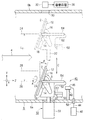
【解決手段】 照明装置40は、真空容器6外に設けられた光源42と、それからの光を真空容器6内へ導くライトガイド44と、真空容器6内に固定されていてライトガイド44で導かれた光48を放出する投光部46と、ホルダ駆動装置10の支持台18に取り付けられていて、ホルダ12がノッチ検出位置28に位置した状態で、投光部46からの光48を受ける受光部50と、それで受けた光を導くライトガイド52と、支持台18に取り付けられていてライトガイド52で導かれた光48を基板2の外周部に照射する発光器54とを備えている。
【選択図】 図2
Description
3 ノッチ
4 イオンビーム
6 真空容器
10 ホルダ駆動装置
12 ホルダ
18 支持台
28 ノッチ検出位置
32 カメラ
36 画像処理装置
40 照明装置
42 光源
44 第1のライトガイド
46 投光部
48 光
50 受光部
52 第2のライトガイド
54 発光器
Claims (2)
- 真空容器内に設けられたホルダに保持された基板にイオンビームを照射してイオン注入を行うイオン注入装置であって、
前記ホルダを前記イオンビームと交差するY方向に機械的に走査する機能を有するホルダ駆動装置と、
前記ホルダに保持された基板の外周部に背面側から光を照射して当該外周部のシルエットを形成する照明装置と、
前記基板の前面側から前記シルエットを撮影するカメラと、
前記カメラからの画像データを処理して、前記基板の外周部に設けられたノッチの位置を検出する画像処理装置とを備えるイオン注入装置において、
(A)前記ホルダ駆動装置は、
(a)前記ホルダを支持するものであって前記Y方向のみに駆動される支持台を備えており、
(b)かつ前記基板のノッチの位置を検出するノッチ検出位置に前記ホルダが位置した状態で前記支持台の位置を固定する機能を有しており、
(B)前記照明装置は、
(a)前記真空容器外に設けられていて光を発する光源と、
(b)前記光源が発する光を前記真空容器内へ導く第1のライトガイドと、
(c)前記真空容器内に固定されていて、前記第1のライトガイドで導かれた光を放出する投光部と、
(d)前記支持台に取り付けられていて、前記ホルダが前記ノッチ検出位置に位置した状態で、前記投光部から放出された光を受ける受光部と、
(e)前記受光部で受けた光を導く第2のライトガイドと、
(f)前記支持台に取り付けられていて、前記第2のライトガイドで導かれた光を、前記ホルダに支持された基板の外周部に背面側から照射して前記シルエットを形成する発光器とを備えている、ことを特徴とするイオン注入装置。 - 前記基板のノッチの位置を検出する時に、遮蔽体を動かして当該遮蔽体によって、前記投光部と受光部との間を前記カメラから隠す遮蔽機構を備えている請求項1記載のイオン注入装置。
Priority Applications (2)
| Application Number | Priority Date | Filing Date | Title |
|---|---|---|---|
| JP2008258718A JP5233012B2 (ja) | 2008-10-03 | 2008-10-03 | イオン注入装置 |
| US12/545,543 US8153995B2 (en) | 2008-10-03 | 2009-08-21 | Ion implanting apparatus |
Applications Claiming Priority (1)
| Application Number | Priority Date | Filing Date | Title |
|---|---|---|---|
| JP2008258718A JP5233012B2 (ja) | 2008-10-03 | 2008-10-03 | イオン注入装置 |
Publications (2)
| Publication Number | Publication Date |
|---|---|
| JP2010092619A true JP2010092619A (ja) | 2010-04-22 |
| JP5233012B2 JP5233012B2 (ja) | 2013-07-10 |
Family
ID=42075064
Family Applications (1)
| Application Number | Title | Priority Date | Filing Date |
|---|---|---|---|
| JP2008258718A Expired - Fee Related JP5233012B2 (ja) | 2008-10-03 | 2008-10-03 | イオン注入装置 |
Country Status (2)
| Country | Link |
|---|---|
| US (1) | US8153995B2 (ja) |
| JP (1) | JP5233012B2 (ja) |
Cited By (1)
| Publication number | Priority date | Publication date | Assignee | Title |
|---|---|---|---|---|
| US10340169B2 (en) | 2015-10-21 | 2019-07-02 | Toshiba Memory Corporation | Antireflection member and orienter apparatus having a third plate part with a second notch part and an antireflection surface |
Families Citing this family (2)
| Publication number | Priority date | Publication date | Assignee | Title |
|---|---|---|---|---|
| US20190148109A1 (en) * | 2017-11-10 | 2019-05-16 | Lam Research Corporation | Method and Apparatus for Anisotropic Pattern Etching and Treatment |
| CN111883539B (zh) * | 2020-08-26 | 2021-09-07 | 长江存储科技有限责任公司 | 三维存储器的制备方法及离子注入装置 |
Citations (6)
| Publication number | Priority date | Publication date | Assignee | Title |
|---|---|---|---|---|
| JPS63161637A (ja) * | 1986-12-25 | 1988-07-05 | Toshiba Corp | 半導体ウエ−ハの位置認識装置 |
| JPH0394447A (ja) * | 1989-09-06 | 1991-04-19 | Yaskawa Electric Mfg Co Ltd | ウエハー位置決め装置 |
| JPH06150871A (ja) * | 1992-11-11 | 1994-05-31 | Nissin Electric Co Ltd | ウェーハ浮き上がり検出装置 |
| JPH09252043A (ja) * | 1996-03-14 | 1997-09-22 | Nikon Corp | 位置決め方法 |
| JPH10134762A (ja) * | 1996-10-29 | 1998-05-22 | Tokyo Electron Ltd | イオン注入装置 |
| JP2006331724A (ja) * | 2005-05-24 | 2006-12-07 | Nissin Ion Equipment Co Ltd | イオンビーム照射装置 |
Family Cites Families (18)
| Publication number | Priority date | Publication date | Assignee | Title |
|---|---|---|---|---|
| DE2940325A1 (de) * | 1979-10-04 | 1981-04-09 | Original Hanau Heraeus Gmbh | Strahlungsmengenmesser |
| CA2073162C (en) * | 1991-07-31 | 1999-06-29 | Lee A. Danisch | Fiber optic bending and positioning sensor |
| JP3282786B2 (ja) | 1996-07-29 | 2002-05-20 | 東芝セラミックス株式会社 | ウエハの形状認識装置 |
| US5845038A (en) * | 1997-01-28 | 1998-12-01 | Minnesota Mining And Manufacturing Company | Optical fiber illumination system |
| JPH1166930A (ja) | 1997-08-11 | 1999-03-09 | Moritex Corp | 照明装置 |
| AU2001295060A1 (en) * | 2000-09-20 | 2002-04-02 | Kla-Tencor-Inc. | Methods and systems for semiconductor fabrication processes |
| US6848822B2 (en) * | 2002-05-31 | 2005-02-01 | 3M Innovative Properties Company | Light guide within recessed housing |
| US7649633B2 (en) * | 2003-11-20 | 2010-01-19 | National Institute Of Advanced Industrial Science And Technology | Method and instrument for measuring complex dielectric constant of a sample by optical spectral measurement |
| US7250611B2 (en) * | 2003-12-02 | 2007-07-31 | 3M Innovative Properties Company | LED curing apparatus and method |
| JP4069081B2 (ja) * | 2004-01-13 | 2008-03-26 | 東京エレクトロン株式会社 | 位置調整方法及び基板処理システム |
| DE102004015326A1 (de) * | 2004-03-30 | 2005-10-20 | Leica Microsystems | Vorrichtung und Verfahren zur Inspektion eines Halbleiterbauteils |
| JP4093235B2 (ja) * | 2005-01-17 | 2008-06-04 | 日新イオン機器株式会社 | イオン注入装置用の角度計測装置および関連装置 |
| US7435951B2 (en) * | 2005-06-08 | 2008-10-14 | Agilent Technologies, Inc. | Ion source sample plate illumination system |
| EP1922419A4 (en) * | 2005-06-10 | 2010-11-17 | Life Technologies Corp | METHOD AND SYSTEM FOR GENETIC MULTIPLEX ANALYSIS |
| US7361914B2 (en) * | 2005-11-30 | 2008-04-22 | Axcelis Technologies, Inc. | Means to establish orientation of ion beam to wafer and correct angle errors |
| JP4930692B2 (ja) * | 2006-06-22 | 2012-05-16 | コニカミノルタビジネステクノロジーズ株式会社 | 画像形成装置 |
| KR100850072B1 (ko) * | 2006-11-03 | 2008-08-04 | 동부일렉트로닉스 주식회사 | 웨이퍼 컷 앵글의 보상 기능을 가지는 이온주입장치 및이를 이용한 이온주입방법 |
| JP4744458B2 (ja) * | 2007-01-31 | 2011-08-10 | 東京エレクトロン株式会社 | 基板位置決め装置および基板位置決め方法 |
-
2008
- 2008-10-03 JP JP2008258718A patent/JP5233012B2/ja not_active Expired - Fee Related
-
2009
- 2009-08-21 US US12/545,543 patent/US8153995B2/en not_active Expired - Fee Related
Patent Citations (6)
| Publication number | Priority date | Publication date | Assignee | Title |
|---|---|---|---|---|
| JPS63161637A (ja) * | 1986-12-25 | 1988-07-05 | Toshiba Corp | 半導体ウエ−ハの位置認識装置 |
| JPH0394447A (ja) * | 1989-09-06 | 1991-04-19 | Yaskawa Electric Mfg Co Ltd | ウエハー位置決め装置 |
| JPH06150871A (ja) * | 1992-11-11 | 1994-05-31 | Nissin Electric Co Ltd | ウェーハ浮き上がり検出装置 |
| JPH09252043A (ja) * | 1996-03-14 | 1997-09-22 | Nikon Corp | 位置決め方法 |
| JPH10134762A (ja) * | 1996-10-29 | 1998-05-22 | Tokyo Electron Ltd | イオン注入装置 |
| JP2006331724A (ja) * | 2005-05-24 | 2006-12-07 | Nissin Ion Equipment Co Ltd | イオンビーム照射装置 |
Cited By (1)
| Publication number | Priority date | Publication date | Assignee | Title |
|---|---|---|---|---|
| US10340169B2 (en) | 2015-10-21 | 2019-07-02 | Toshiba Memory Corporation | Antireflection member and orienter apparatus having a third plate part with a second notch part and an antireflection surface |
Also Published As
| Publication number | Publication date |
|---|---|
| US8153995B2 (en) | 2012-04-10 |
| JP5233012B2 (ja) | 2013-07-10 |
| US20100084584A1 (en) | 2010-04-08 |
Similar Documents
| Publication | Publication Date | Title |
|---|---|---|
| US8837777B2 (en) | Wafer detecting apparatus | |
| US8220714B2 (en) | Scanner | |
| JP5185756B2 (ja) | 基板検出装置および方法 | |
| JP3472750B2 (ja) | 表面検査装置 | |
| CN108369330A (zh) | 观察装置 | |
| JP5233012B2 (ja) | イオン注入装置 | |
| US9521287B2 (en) | Light guide, illuminating device for image reading, and image reading apparatus | |
| JP6097460B2 (ja) | 画像読取ユニット | |
| CN116359236A (zh) | 检测装置 | |
| KR101658700B1 (ko) | 표면 검사 광학장치 및 표면 검사방법 | |
| CN107148631B (zh) | 用于容器侧壁上的浮凸部的光学读取的方法、装置和检验线 | |
| JP6486767B2 (ja) | 固定式の光学的情報読取装置およびそれを用いた光学的情報読取方法 | |
| JP2015102364A (ja) | 外観検査装置 | |
| KR102581986B1 (ko) | 릴레이티브 액티브 얼라인 장치 | |
| JP2020064734A (ja) | 照明装置 | |
| TW201224440A (en) | Inspection device | |
| JP4721733B2 (ja) | 撮像装置 | |
| JP6001361B2 (ja) | 電子部品の搭載方法、部品搭載ヘッドおよび電子部品搭載装置 | |
| JP2016170225A (ja) | 照明装置、照明装置を備えた画像読取装置、及び導光部材 | |
| JP6393667B2 (ja) | 外観検査装置および外観検査方法 | |
| JP5087520B2 (ja) | イメージセンサモジュール | |
| JP5085599B2 (ja) | 部品保持装置、電子部品認識装置及び電子部品装着装置 | |
| US10893640B2 (en) | Component pickup apparatus | |
| JP2009104032A (ja) | 照明装置および画像読取装置 | |
| JP2005093818A (ja) | 撮像装置 |
Legal Events
| Date | Code | Title | Description |
|---|---|---|---|
| A621 | Written request for application examination |
Free format text: JAPANESE INTERMEDIATE CODE: A621 Effective date: 20110217 |
|
| A521 | Request for written amendment filed |
Free format text: JAPANESE INTERMEDIATE CODE: A523 Effective date: 20111107 |
|
| TRDD | Decision of grant or rejection written | ||
| A01 | Written decision to grant a patent or to grant a registration (utility model) |
Free format text: JAPANESE INTERMEDIATE CODE: A01 Effective date: 20130219 |
|
| A61 | First payment of annual fees (during grant procedure) |
Free format text: JAPANESE INTERMEDIATE CODE: A61 Effective date: 20130304 |
|
| R150 | Certificate of patent or registration of utility model |
Free format text: JAPANESE INTERMEDIATE CODE: R150 |
|
| FPAY | Renewal fee payment (event date is renewal date of database) |
Free format text: PAYMENT UNTIL: 20160405 Year of fee payment: 3 |
|
| R250 | Receipt of annual fees |
Free format text: JAPANESE INTERMEDIATE CODE: R250 |
|
| R250 | Receipt of annual fees |
Free format text: JAPANESE INTERMEDIATE CODE: R250 |
|
| LAPS | Cancellation because of no payment of annual fees |