JP2010087502A - メモリデバイスを実現する積層チップパッケージ - Google Patents
メモリデバイスを実現する積層チップパッケージ Download PDFInfo
- Publication number
- JP2010087502A JP2010087502A JP2009207677A JP2009207677A JP2010087502A JP 2010087502 A JP2010087502 A JP 2010087502A JP 2009207677 A JP2009207677 A JP 2009207677A JP 2009207677 A JP2009207677 A JP 2009207677A JP 2010087502 A JP2010087502 A JP 2010087502A
- Authority
- JP
- Japan
- Prior art keywords
- main body
- wiring
- disposed
- type
- semiconductor chip
- Prior art date
- Legal status (The legal status is an assumption and is not a legal conclusion. Google has not performed a legal analysis and makes no representation as to the accuracy of the status listed.)
- Granted
Links
- 239000004065 semiconductor Substances 0.000 claims abstract description 137
- 239000010410 layer Substances 0.000 description 261
- 238000005498 polishing Methods 0.000 description 86
- 238000000034 method Methods 0.000 description 81
- 235000012431 wafers Nutrition 0.000 description 79
- 238000004519 manufacturing process Methods 0.000 description 29
- 230000002950 deficient Effects 0.000 description 22
- 238000007747 plating Methods 0.000 description 16
- 229910000679 solder Inorganic materials 0.000 description 14
- 239000011347 resin Substances 0.000 description 13
- 229920005989 resin Polymers 0.000 description 13
- 230000000712 assembly Effects 0.000 description 11
- 238000000429 assembly Methods 0.000 description 11
- 238000005520 cutting process Methods 0.000 description 11
- 239000000853 adhesive Substances 0.000 description 7
- 230000001070 adhesive effect Effects 0.000 description 7
- 239000000463 material Substances 0.000 description 7
- 239000000758 substrate Substances 0.000 description 6
- 238000005530 etching Methods 0.000 description 5
- 230000010354 integration Effects 0.000 description 5
- 230000000694 effects Effects 0.000 description 4
- 238000000227 grinding Methods 0.000 description 4
- 239000011810 insulating material Substances 0.000 description 4
- 238000000206 photolithography Methods 0.000 description 4
- 229920001721 polyimide Polymers 0.000 description 4
- 239000009719 polyimide resin Substances 0.000 description 4
- XUIMIQQOPSSXEZ-UHFFFAOYSA-N Silicon Chemical compound [Si] XUIMIQQOPSSXEZ-UHFFFAOYSA-N 0.000 description 3
- 239000002184 metal Substances 0.000 description 3
- 230000002093 peripheral effect Effects 0.000 description 3
- 229920002120 photoresistant polymer Polymers 0.000 description 3
- 229910052710 silicon Inorganic materials 0.000 description 3
- 239000010703 silicon Substances 0.000 description 3
- 230000015572 biosynthetic process Effects 0.000 description 2
- 239000003795 chemical substances by application Substances 0.000 description 2
- 238000005516 engineering process Methods 0.000 description 2
- 239000003822 epoxy resin Substances 0.000 description 2
- 230000006870 function Effects 0.000 description 2
- 238000005304 joining Methods 0.000 description 2
- 238000010030 laminating Methods 0.000 description 2
- 238000000059 patterning Methods 0.000 description 2
- 229920000647 polyepoxide Polymers 0.000 description 2
- 206010034972 Photosensitivity reaction Diseases 0.000 description 1
- NIXOWILDQLNWCW-UHFFFAOYSA-N acrylic acid group Chemical group C(C=C)(=O)O NIXOWILDQLNWCW-UHFFFAOYSA-N 0.000 description 1
- 239000000919 ceramic Substances 0.000 description 1
- 239000004020 conductor Substances 0.000 description 1
- 230000008602 contraction Effects 0.000 description 1
- 238000010586 diagram Methods 0.000 description 1
- 238000006073 displacement reaction Methods 0.000 description 1
- 229920005570 flexible polymer Polymers 0.000 description 1
- 239000011521 glass Substances 0.000 description 1
- 238000010438 heat treatment Methods 0.000 description 1
- 230000036211 photosensitivity Effects 0.000 description 1
- 238000001020 plasma etching Methods 0.000 description 1
- 230000001681 protective effect Effects 0.000 description 1
- 239000011241 protective layer Substances 0.000 description 1
- 239000012780 transparent material Substances 0.000 description 1
Images


Classifications
-
- H—ELECTRICITY
- H01—ELECTRIC ELEMENTS
- H01L—SEMICONDUCTOR DEVICES NOT COVERED BY CLASS H10
- H01L25/00—Assemblies consisting of a plurality of individual semiconductor or other solid state devices ; Multistep manufacturing processes thereof
- H01L25/03—Assemblies consisting of a plurality of individual semiconductor or other solid state devices ; Multistep manufacturing processes thereof all the devices being of a type provided for in the same subgroup of groups H01L27/00 - H01L33/00, or in a single subclass of H10K, H10N, e.g. assemblies of rectifier diodes
- H01L25/04—Assemblies consisting of a plurality of individual semiconductor or other solid state devices ; Multistep manufacturing processes thereof all the devices being of a type provided for in the same subgroup of groups H01L27/00 - H01L33/00, or in a single subclass of H10K, H10N, e.g. assemblies of rectifier diodes the devices not having separate containers
- H01L25/065—Assemblies consisting of a plurality of individual semiconductor or other solid state devices ; Multistep manufacturing processes thereof all the devices being of a type provided for in the same subgroup of groups H01L27/00 - H01L33/00, or in a single subclass of H10K, H10N, e.g. assemblies of rectifier diodes the devices not having separate containers the devices being of a type provided for in group H01L27/00
- H01L25/0657—Stacked arrangements of devices
-
- H—ELECTRICITY
- H01—ELECTRIC ELEMENTS
- H01L—SEMICONDUCTOR DEVICES NOT COVERED BY CLASS H10
- H01L21/00—Processes or apparatus adapted for the manufacture or treatment of semiconductor or solid state devices or of parts thereof
- H01L21/67—Apparatus specially adapted for handling semiconductor or electric solid state devices during manufacture or treatment thereof; Apparatus specially adapted for handling wafers during manufacture or treatment of semiconductor or electric solid state devices or components ; Apparatus not specifically provided for elsewhere
- H01L21/683—Apparatus specially adapted for handling semiconductor or electric solid state devices during manufacture or treatment thereof; Apparatus specially adapted for handling wafers during manufacture or treatment of semiconductor or electric solid state devices or components ; Apparatus not specifically provided for elsewhere for supporting or gripping
- H01L21/6835—Apparatus specially adapted for handling semiconductor or electric solid state devices during manufacture or treatment thereof; Apparatus specially adapted for handling wafers during manufacture or treatment of semiconductor or electric solid state devices or components ; Apparatus not specifically provided for elsewhere for supporting or gripping using temporarily an auxiliary support
-
- H—ELECTRICITY
- H01—ELECTRIC ELEMENTS
- H01L—SEMICONDUCTOR DEVICES NOT COVERED BY CLASS H10
- H01L23/00—Details of semiconductor or other solid state devices
- H01L23/544—Marks applied to semiconductor devices or parts, e.g. registration marks, alignment structures, wafer maps
-
- H—ELECTRICITY
- H01—ELECTRIC ELEMENTS
- H01L—SEMICONDUCTOR DEVICES NOT COVERED BY CLASS H10
- H01L24/00—Arrangements for connecting or disconnecting semiconductor or solid-state bodies; Methods or apparatus related thereto
- H01L24/01—Means for bonding being attached to, or being formed on, the surface to be connected, e.g. chip-to-package, die-attach, "first-level" interconnects; Manufacturing methods related thereto
- H01L24/18—High density interconnect [HDI] connectors; Manufacturing methods related thereto
- H01L24/23—Structure, shape, material or disposition of the high density interconnect connectors after the connecting process
- H01L24/24—Structure, shape, material or disposition of the high density interconnect connectors after the connecting process of an individual high density interconnect connector
-
- H—ELECTRICITY
- H01—ELECTRIC ELEMENTS
- H01L—SEMICONDUCTOR DEVICES NOT COVERED BY CLASS H10
- H01L24/00—Arrangements for connecting or disconnecting semiconductor or solid-state bodies; Methods or apparatus related thereto
- H01L24/01—Means for bonding being attached to, or being formed on, the surface to be connected, e.g. chip-to-package, die-attach, "first-level" interconnects; Manufacturing methods related thereto
- H01L24/18—High density interconnect [HDI] connectors; Manufacturing methods related thereto
- H01L24/23—Structure, shape, material or disposition of the high density interconnect connectors after the connecting process
- H01L24/25—Structure, shape, material or disposition of the high density interconnect connectors after the connecting process of a plurality of high density interconnect connectors
-
- H—ELECTRICITY
- H01—ELECTRIC ELEMENTS
- H01L—SEMICONDUCTOR DEVICES NOT COVERED BY CLASS H10
- H01L24/00—Arrangements for connecting or disconnecting semiconductor or solid-state bodies; Methods or apparatus related thereto
- H01L24/01—Means for bonding being attached to, or being formed on, the surface to be connected, e.g. chip-to-package, die-attach, "first-level" interconnects; Manufacturing methods related thereto
- H01L24/42—Wire connectors; Manufacturing methods related thereto
- H01L24/47—Structure, shape, material or disposition of the wire connectors after the connecting process
- H01L24/48—Structure, shape, material or disposition of the wire connectors after the connecting process of an individual wire connector
-
- H—ELECTRICITY
- H01—ELECTRIC ELEMENTS
- H01L—SEMICONDUCTOR DEVICES NOT COVERED BY CLASS H10
- H01L24/00—Arrangements for connecting or disconnecting semiconductor or solid-state bodies; Methods or apparatus related thereto
- H01L24/73—Means for bonding being of different types provided for in two or more of groups H01L24/10, H01L24/18, H01L24/26, H01L24/34, H01L24/42, H01L24/50, H01L24/63, H01L24/71
-
- H—ELECTRICITY
- H01—ELECTRIC ELEMENTS
- H01L—SEMICONDUCTOR DEVICES NOT COVERED BY CLASS H10
- H01L24/00—Arrangements for connecting or disconnecting semiconductor or solid-state bodies; Methods or apparatus related thereto
- H01L24/80—Methods for connecting semiconductor or other solid state bodies using means for bonding being attached to, or being formed on, the surface to be connected
- H01L24/82—Methods for connecting semiconductor or other solid state bodies using means for bonding being attached to, or being formed on, the surface to be connected by forming build-up interconnects at chip-level, e.g. for high density interconnects [HDI]
-
- H—ELECTRICITY
- H01—ELECTRIC ELEMENTS
- H01L—SEMICONDUCTOR DEVICES NOT COVERED BY CLASS H10
- H01L24/00—Arrangements for connecting or disconnecting semiconductor or solid-state bodies; Methods or apparatus related thereto
- H01L24/93—Batch processes
- H01L24/94—Batch processes at wafer-level, i.e. with connecting carried out on a wafer comprising a plurality of undiced individual devices
-
- H—ELECTRICITY
- H01—ELECTRIC ELEMENTS
- H01L—SEMICONDUCTOR DEVICES NOT COVERED BY CLASS H10
- H01L24/00—Arrangements for connecting or disconnecting semiconductor or solid-state bodies; Methods or apparatus related thereto
- H01L24/93—Batch processes
- H01L24/95—Batch processes at chip-level, i.e. with connecting carried out on a plurality of singulated devices, i.e. on diced chips
- H01L24/96—Batch processes at chip-level, i.e. with connecting carried out on a plurality of singulated devices, i.e. on diced chips the devices being encapsulated in a common layer, e.g. neo-wafer or pseudo-wafer, said common layer being separable into individual assemblies after connecting
-
- H—ELECTRICITY
- H01—ELECTRIC ELEMENTS
- H01L—SEMICONDUCTOR DEVICES NOT COVERED BY CLASS H10
- H01L25/00—Assemblies consisting of a plurality of individual semiconductor or other solid state devices ; Multistep manufacturing processes thereof
- H01L25/03—Assemblies consisting of a plurality of individual semiconductor or other solid state devices ; Multistep manufacturing processes thereof all the devices being of a type provided for in the same subgroup of groups H01L27/00 - H01L33/00, or in a single subclass of H10K, H10N, e.g. assemblies of rectifier diodes
- H01L25/10—Assemblies consisting of a plurality of individual semiconductor or other solid state devices ; Multistep manufacturing processes thereof all the devices being of a type provided for in the same subgroup of groups H01L27/00 - H01L33/00, or in a single subclass of H10K, H10N, e.g. assemblies of rectifier diodes the devices having separate containers
- H01L25/105—Assemblies consisting of a plurality of individual semiconductor or other solid state devices ; Multistep manufacturing processes thereof all the devices being of a type provided for in the same subgroup of groups H01L27/00 - H01L33/00, or in a single subclass of H10K, H10N, e.g. assemblies of rectifier diodes the devices having separate containers the devices being of a type provided for in group H01L27/00
-
- H—ELECTRICITY
- H01—ELECTRIC ELEMENTS
- H01L—SEMICONDUCTOR DEVICES NOT COVERED BY CLASS H10
- H01L25/00—Assemblies consisting of a plurality of individual semiconductor or other solid state devices ; Multistep manufacturing processes thereof
- H01L25/16—Assemblies consisting of a plurality of individual semiconductor or other solid state devices ; Multistep manufacturing processes thereof the devices being of types provided for in two or more different main groups of groups H01L27/00 - H01L33/00, or in a single subclass of H10K, H10N, e.g. forming hybrid circuits
-
- H—ELECTRICITY
- H01—ELECTRIC ELEMENTS
- H01L—SEMICONDUCTOR DEVICES NOT COVERED BY CLASS H10
- H01L25/00—Assemblies consisting of a plurality of individual semiconductor or other solid state devices ; Multistep manufacturing processes thereof
- H01L25/18—Assemblies consisting of a plurality of individual semiconductor or other solid state devices ; Multistep manufacturing processes thereof the devices being of types provided for in two or more different subgroups of the same main group of groups H01L27/00 - H01L33/00, or in a single subclass of H10K, H10N
-
- H—ELECTRICITY
- H01—ELECTRIC ELEMENTS
- H01L—SEMICONDUCTOR DEVICES NOT COVERED BY CLASS H10
- H01L25/00—Assemblies consisting of a plurality of individual semiconductor or other solid state devices ; Multistep manufacturing processes thereof
- H01L25/50—Multistep manufacturing processes of assemblies consisting of devices, each device being of a type provided for in group H01L27/00 or H01L29/00
-
- H—ELECTRICITY
- H01—ELECTRIC ELEMENTS
- H01L—SEMICONDUCTOR DEVICES NOT COVERED BY CLASS H10
- H01L2221/00—Processes or apparatus adapted for the manufacture or treatment of semiconductor or solid state devices or of parts thereof covered by H01L21/00
- H01L2221/67—Apparatus for handling semiconductor or electric solid state devices during manufacture or treatment thereof; Apparatus for handling wafers during manufacture or treatment of semiconductor or electric solid state devices or components; Apparatus not specifically provided for elsewhere
- H01L2221/683—Apparatus for handling semiconductor or electric solid state devices during manufacture or treatment thereof; Apparatus for handling wafers during manufacture or treatment of semiconductor or electric solid state devices or components; Apparatus not specifically provided for elsewhere for supporting or gripping
- H01L2221/68304—Apparatus for handling semiconductor or electric solid state devices during manufacture or treatment thereof; Apparatus for handling wafers during manufacture or treatment of semiconductor or electric solid state devices or components; Apparatus not specifically provided for elsewhere for supporting or gripping using temporarily an auxiliary support
- H01L2221/68359—Apparatus for handling semiconductor or electric solid state devices during manufacture or treatment thereof; Apparatus for handling wafers during manufacture or treatment of semiconductor or electric solid state devices or components; Apparatus not specifically provided for elsewhere for supporting or gripping using temporarily an auxiliary support used as a support during manufacture of interconnect decals or build up layers
-
- H—ELECTRICITY
- H01—ELECTRIC ELEMENTS
- H01L—SEMICONDUCTOR DEVICES NOT COVERED BY CLASS H10
- H01L2223/00—Details relating to semiconductor or other solid state devices covered by the group H01L23/00
- H01L2223/544—Marks applied to semiconductor devices or parts
- H01L2223/5442—Marks applied to semiconductor devices or parts comprising non digital, non alphanumeric information, e.g. symbols
-
- H—ELECTRICITY
- H01—ELECTRIC ELEMENTS
- H01L—SEMICONDUCTOR DEVICES NOT COVERED BY CLASS H10
- H01L2223/00—Details relating to semiconductor or other solid state devices covered by the group H01L23/00
- H01L2223/544—Marks applied to semiconductor devices or parts
- H01L2223/54426—Marks applied to semiconductor devices or parts for alignment
-
- H—ELECTRICITY
- H01—ELECTRIC ELEMENTS
- H01L—SEMICONDUCTOR DEVICES NOT COVERED BY CLASS H10
- H01L2224/00—Indexing scheme for arrangements for connecting or disconnecting semiconductor or solid-state bodies and methods related thereto as covered by H01L24/00
- H01L2224/01—Means for bonding being attached to, or being formed on, the surface to be connected, e.g. chip-to-package, die-attach, "first-level" interconnects; Manufacturing methods related thereto
- H01L2224/10—Bump connectors; Manufacturing methods related thereto
- H01L2224/15—Structure, shape, material or disposition of the bump connectors after the connecting process
- H01L2224/16—Structure, shape, material or disposition of the bump connectors after the connecting process of an individual bump connector
-
- H—ELECTRICITY
- H01—ELECTRIC ELEMENTS
- H01L—SEMICONDUCTOR DEVICES NOT COVERED BY CLASS H10
- H01L2224/00—Indexing scheme for arrangements for connecting or disconnecting semiconductor or solid-state bodies and methods related thereto as covered by H01L24/00
- H01L2224/01—Means for bonding being attached to, or being formed on, the surface to be connected, e.g. chip-to-package, die-attach, "first-level" interconnects; Manufacturing methods related thereto
- H01L2224/18—High density interconnect [HDI] connectors; Manufacturing methods related thereto
- H01L2224/23—Structure, shape, material or disposition of the high density interconnect connectors after the connecting process
- H01L2224/24—Structure, shape, material or disposition of the high density interconnect connectors after the connecting process of an individual high density interconnect connector
- H01L2224/241—Disposition
- H01L2224/24135—Connecting between different semiconductor or solid-state bodies, i.e. chip-to-chip
- H01L2224/24137—Connecting between different semiconductor or solid-state bodies, i.e. chip-to-chip the bodies being arranged next to each other, e.g. on a common substrate
-
- H—ELECTRICITY
- H01—ELECTRIC ELEMENTS
- H01L—SEMICONDUCTOR DEVICES NOT COVERED BY CLASS H10
- H01L2224/00—Indexing scheme for arrangements for connecting or disconnecting semiconductor or solid-state bodies and methods related thereto as covered by H01L24/00
- H01L2224/01—Means for bonding being attached to, or being formed on, the surface to be connected, e.g. chip-to-package, die-attach, "first-level" interconnects; Manufacturing methods related thereto
- H01L2224/42—Wire connectors; Manufacturing methods related thereto
- H01L2224/47—Structure, shape, material or disposition of the wire connectors after the connecting process
- H01L2224/48—Structure, shape, material or disposition of the wire connectors after the connecting process of an individual wire connector
- H01L2224/4805—Shape
- H01L2224/4809—Loop shape
- H01L2224/48091—Arched
-
- H—ELECTRICITY
- H01—ELECTRIC ELEMENTS
- H01L—SEMICONDUCTOR DEVICES NOT COVERED BY CLASS H10
- H01L2224/00—Indexing scheme for arrangements for connecting or disconnecting semiconductor or solid-state bodies and methods related thereto as covered by H01L24/00
- H01L2224/01—Means for bonding being attached to, or being formed on, the surface to be connected, e.g. chip-to-package, die-attach, "first-level" interconnects; Manufacturing methods related thereto
- H01L2224/42—Wire connectors; Manufacturing methods related thereto
- H01L2224/47—Structure, shape, material or disposition of the wire connectors after the connecting process
- H01L2224/48—Structure, shape, material or disposition of the wire connectors after the connecting process of an individual wire connector
- H01L2224/484—Connecting portions
- H01L2224/48463—Connecting portions the connecting portion on the bonding area of the semiconductor or solid-state body being a ball bond
- H01L2224/48464—Connecting portions the connecting portion on the bonding area of the semiconductor or solid-state body being a ball bond the other connecting portion not on the bonding area also being a ball bond, i.e. ball-to-ball
-
- H—ELECTRICITY
- H01—ELECTRIC ELEMENTS
- H01L—SEMICONDUCTOR DEVICES NOT COVERED BY CLASS H10
- H01L2224/00—Indexing scheme for arrangements for connecting or disconnecting semiconductor or solid-state bodies and methods related thereto as covered by H01L24/00
- H01L2224/01—Means for bonding being attached to, or being formed on, the surface to be connected, e.g. chip-to-package, die-attach, "first-level" interconnects; Manufacturing methods related thereto
- H01L2224/42—Wire connectors; Manufacturing methods related thereto
- H01L2224/47—Structure, shape, material or disposition of the wire connectors after the connecting process
- H01L2224/49—Structure, shape, material or disposition of the wire connectors after the connecting process of a plurality of wire connectors
- H01L2224/491—Disposition
- H01L2224/4912—Layout
- H01L2224/49175—Parallel arrangements
-
- H—ELECTRICITY
- H01—ELECTRIC ELEMENTS
- H01L—SEMICONDUCTOR DEVICES NOT COVERED BY CLASS H10
- H01L2224/00—Indexing scheme for arrangements for connecting or disconnecting semiconductor or solid-state bodies and methods related thereto as covered by H01L24/00
- H01L2224/01—Means for bonding being attached to, or being formed on, the surface to be connected, e.g. chip-to-package, die-attach, "first-level" interconnects; Manufacturing methods related thereto
- H01L2224/42—Wire connectors; Manufacturing methods related thereto
- H01L2224/47—Structure, shape, material or disposition of the wire connectors after the connecting process
- H01L2224/49—Structure, shape, material or disposition of the wire connectors after the connecting process of a plurality of wire connectors
- H01L2224/494—Connecting portions
- H01L2224/4943—Connecting portions the connecting portions being staggered
-
- H—ELECTRICITY
- H01—ELECTRIC ELEMENTS
- H01L—SEMICONDUCTOR DEVICES NOT COVERED BY CLASS H10
- H01L2224/00—Indexing scheme for arrangements for connecting or disconnecting semiconductor or solid-state bodies and methods related thereto as covered by H01L24/00
- H01L2224/73—Means for bonding being of different types provided for in two or more of groups H01L2224/10, H01L2224/18, H01L2224/26, H01L2224/34, H01L2224/42, H01L2224/50, H01L2224/63, H01L2224/71
- H01L2224/732—Location after the connecting process
- H01L2224/73251—Location after the connecting process on different surfaces
- H01L2224/73267—Layer and HDI connectors
-
- H—ELECTRICITY
- H01—ELECTRIC ELEMENTS
- H01L—SEMICONDUCTOR DEVICES NOT COVERED BY CLASS H10
- H01L2225/00—Details relating to assemblies covered by the group H01L25/00 but not provided for in its subgroups
- H01L2225/03—All the devices being of a type provided for in the same subgroup of groups H01L27/00 - H01L33/648 and H10K99/00
- H01L2225/04—All the devices being of a type provided for in the same subgroup of groups H01L27/00 - H01L33/648 and H10K99/00 the devices not having separate containers
- H01L2225/065—All the devices being of a type provided for in the same subgroup of groups H01L27/00 - H01L33/648 and H10K99/00 the devices not having separate containers the devices being of a type provided for in group H01L27/00
- H01L2225/06503—Stacked arrangements of devices
- H01L2225/06513—Bump or bump-like direct electrical connections between devices, e.g. flip-chip connection, solder bumps
-
- H—ELECTRICITY
- H01—ELECTRIC ELEMENTS
- H01L—SEMICONDUCTOR DEVICES NOT COVERED BY CLASS H10
- H01L2225/00—Details relating to assemblies covered by the group H01L25/00 but not provided for in its subgroups
- H01L2225/03—All the devices being of a type provided for in the same subgroup of groups H01L27/00 - H01L33/648 and H10K99/00
- H01L2225/04—All the devices being of a type provided for in the same subgroup of groups H01L27/00 - H01L33/648 and H10K99/00 the devices not having separate containers
- H01L2225/065—All the devices being of a type provided for in the same subgroup of groups H01L27/00 - H01L33/648 and H10K99/00 the devices not having separate containers the devices being of a type provided for in group H01L27/00
- H01L2225/06503—Stacked arrangements of devices
- H01L2225/06524—Electrical connections formed on device or on substrate, e.g. a deposited or grown layer
-
- H—ELECTRICITY
- H01—ELECTRIC ELEMENTS
- H01L—SEMICONDUCTOR DEVICES NOT COVERED BY CLASS H10
- H01L2225/00—Details relating to assemblies covered by the group H01L25/00 but not provided for in its subgroups
- H01L2225/03—All the devices being of a type provided for in the same subgroup of groups H01L27/00 - H01L33/648 and H10K99/00
- H01L2225/04—All the devices being of a type provided for in the same subgroup of groups H01L27/00 - H01L33/648 and H10K99/00 the devices not having separate containers
- H01L2225/065—All the devices being of a type provided for in the same subgroup of groups H01L27/00 - H01L33/648 and H10K99/00 the devices not having separate containers the devices being of a type provided for in group H01L27/00
- H01L2225/06503—Stacked arrangements of devices
- H01L2225/06551—Conductive connections on the side of the device
-
- H—ELECTRICITY
- H01—ELECTRIC ELEMENTS
- H01L—SEMICONDUCTOR DEVICES NOT COVERED BY CLASS H10
- H01L2225/00—Details relating to assemblies covered by the group H01L25/00 but not provided for in its subgroups
- H01L2225/03—All the devices being of a type provided for in the same subgroup of groups H01L27/00 - H01L33/648 and H10K99/00
- H01L2225/10—All the devices being of a type provided for in the same subgroup of groups H01L27/00 - H01L33/648 and H10K99/00 the devices having separate containers
- H01L2225/1005—All the devices being of a type provided for in the same subgroup of groups H01L27/00 - H01L33/648 and H10K99/00 the devices having separate containers the devices being of a type provided for in group H01L27/00
- H01L2225/1011—All the devices being of a type provided for in the same subgroup of groups H01L27/00 - H01L33/648 and H10K99/00 the devices having separate containers the devices being of a type provided for in group H01L27/00 the containers being in a stacked arrangement
- H01L2225/1047—Details of electrical connections between containers
- H01L2225/1058—Bump or bump-like electrical connections, e.g. balls, pillars, posts
-
- H—ELECTRICITY
- H01—ELECTRIC ELEMENTS
- H01L—SEMICONDUCTOR DEVICES NOT COVERED BY CLASS H10
- H01L24/00—Arrangements for connecting or disconnecting semiconductor or solid-state bodies; Methods or apparatus related thereto
- H01L24/01—Means for bonding being attached to, or being formed on, the surface to be connected, e.g. chip-to-package, die-attach, "first-level" interconnects; Manufacturing methods related thereto
- H01L24/42—Wire connectors; Manufacturing methods related thereto
- H01L24/47—Structure, shape, material or disposition of the wire connectors after the connecting process
- H01L24/49—Structure, shape, material or disposition of the wire connectors after the connecting process of a plurality of wire connectors
-
- H—ELECTRICITY
- H01—ELECTRIC ELEMENTS
- H01L—SEMICONDUCTOR DEVICES NOT COVERED BY CLASS H10
- H01L2924/00—Indexing scheme for arrangements or methods for connecting or disconnecting semiconductor or solid-state bodies as covered by H01L24/00
- H01L2924/0001—Technical content checked by a classifier
- H01L2924/00014—Technical content checked by a classifier the subject-matter covered by the group, the symbol of which is combined with the symbol of this group, being disclosed without further technical details
-
- H—ELECTRICITY
- H01—ELECTRIC ELEMENTS
- H01L—SEMICONDUCTOR DEVICES NOT COVERED BY CLASS H10
- H01L2924/00—Indexing scheme for arrangements or methods for connecting or disconnecting semiconductor or solid-state bodies as covered by H01L24/00
- H01L2924/01—Chemical elements
- H01L2924/01004—Beryllium [Be]
-
- H—ELECTRICITY
- H01—ELECTRIC ELEMENTS
- H01L—SEMICONDUCTOR DEVICES NOT COVERED BY CLASS H10
- H01L2924/00—Indexing scheme for arrangements or methods for connecting or disconnecting semiconductor or solid-state bodies as covered by H01L24/00
- H01L2924/01—Chemical elements
- H01L2924/01006—Carbon [C]
-
- H—ELECTRICITY
- H01—ELECTRIC ELEMENTS
- H01L—SEMICONDUCTOR DEVICES NOT COVERED BY CLASS H10
- H01L2924/00—Indexing scheme for arrangements or methods for connecting or disconnecting semiconductor or solid-state bodies as covered by H01L24/00
- H01L2924/01—Chemical elements
- H01L2924/01014—Silicon [Si]
-
- H—ELECTRICITY
- H01—ELECTRIC ELEMENTS
- H01L—SEMICONDUCTOR DEVICES NOT COVERED BY CLASS H10
- H01L2924/00—Indexing scheme for arrangements or methods for connecting or disconnecting semiconductor or solid-state bodies as covered by H01L24/00
- H01L2924/01—Chemical elements
- H01L2924/01015—Phosphorus [P]
-
- H—ELECTRICITY
- H01—ELECTRIC ELEMENTS
- H01L—SEMICONDUCTOR DEVICES NOT COVERED BY CLASS H10
- H01L2924/00—Indexing scheme for arrangements or methods for connecting or disconnecting semiconductor or solid-state bodies as covered by H01L24/00
- H01L2924/01—Chemical elements
- H01L2924/01029—Copper [Cu]
-
- H—ELECTRICITY
- H01—ELECTRIC ELEMENTS
- H01L—SEMICONDUCTOR DEVICES NOT COVERED BY CLASS H10
- H01L2924/00—Indexing scheme for arrangements or methods for connecting or disconnecting semiconductor or solid-state bodies as covered by H01L24/00
- H01L2924/01—Chemical elements
- H01L2924/01033—Arsenic [As]
-
- H—ELECTRICITY
- H01—ELECTRIC ELEMENTS
- H01L—SEMICONDUCTOR DEVICES NOT COVERED BY CLASS H10
- H01L2924/00—Indexing scheme for arrangements or methods for connecting or disconnecting semiconductor or solid-state bodies as covered by H01L24/00
- H01L2924/01—Chemical elements
- H01L2924/01075—Rhenium [Re]
-
- H—ELECTRICITY
- H01—ELECTRIC ELEMENTS
- H01L—SEMICONDUCTOR DEVICES NOT COVERED BY CLASS H10
- H01L2924/00—Indexing scheme for arrangements or methods for connecting or disconnecting semiconductor or solid-state bodies as covered by H01L24/00
- H01L2924/01—Chemical elements
- H01L2924/01078—Platinum [Pt]
-
- H—ELECTRICITY
- H01—ELECTRIC ELEMENTS
- H01L—SEMICONDUCTOR DEVICES NOT COVERED BY CLASS H10
- H01L2924/00—Indexing scheme for arrangements or methods for connecting or disconnecting semiconductor or solid-state bodies as covered by H01L24/00
- H01L2924/01—Chemical elements
- H01L2924/01082—Lead [Pb]
-
- H—ELECTRICITY
- H01—ELECTRIC ELEMENTS
- H01L—SEMICONDUCTOR DEVICES NOT COVERED BY CLASS H10
- H01L2924/00—Indexing scheme for arrangements or methods for connecting or disconnecting semiconductor or solid-state bodies as covered by H01L24/00
- H01L2924/013—Alloys
- H01L2924/014—Solder alloys
-
- H—ELECTRICITY
- H01—ELECTRIC ELEMENTS
- H01L—SEMICONDUCTOR DEVICES NOT COVERED BY CLASS H10
- H01L2924/00—Indexing scheme for arrangements or methods for connecting or disconnecting semiconductor or solid-state bodies as covered by H01L24/00
- H01L2924/06—Polymers
- H01L2924/078—Adhesive characteristics other than chemical
- H01L2924/07802—Adhesive characteristics other than chemical not being an ohmic electrical conductor
-
- H—ELECTRICITY
- H01—ELECTRIC ELEMENTS
- H01L—SEMICONDUCTOR DEVICES NOT COVERED BY CLASS H10
- H01L2924/00—Indexing scheme for arrangements or methods for connecting or disconnecting semiconductor or solid-state bodies as covered by H01L24/00
- H01L2924/10—Details of semiconductor or other solid state devices to be connected
- H01L2924/102—Material of the semiconductor or solid state bodies
- H01L2924/1025—Semiconducting materials
- H01L2924/10251—Elemental semiconductors, i.e. Group IV
- H01L2924/10253—Silicon [Si]
-
- H—ELECTRICITY
- H01—ELECTRIC ELEMENTS
- H01L—SEMICONDUCTOR DEVICES NOT COVERED BY CLASS H10
- H01L2924/00—Indexing scheme for arrangements or methods for connecting or disconnecting semiconductor or solid-state bodies as covered by H01L24/00
- H01L2924/15—Details of package parts other than the semiconductor or other solid state devices to be connected
- H01L2924/181—Encapsulation
-
- H—ELECTRICITY
- H01—ELECTRIC ELEMENTS
- H01L—SEMICONDUCTOR DEVICES NOT COVERED BY CLASS H10
- H01L2924/00—Indexing scheme for arrangements or methods for connecting or disconnecting semiconductor or solid-state bodies as covered by H01L24/00
- H01L2924/30—Technical effects
- H01L2924/301—Electrical effects
- H01L2924/30105—Capacitance
Abstract
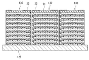
【解決手段】積層チップパッケージ1は、本体2と、本体2の側面に配置された配線3A,3Bとを備えている。本体2は、それぞれ第1の種類の半導体チップを含む複数の第1の種類の階層部分12〜18と、第2の種類の半導体チップを含む第2の種類の階層部分11とを含んでいる。第1の種類の半導体チップは、複数のメモリセルを含んでいる。第2の種類の半導体チップは、複数の第1の種類の階層部分に含まれる複数のメモリセルに対する書き込みと読み出しを制御する回路を含んでいる。各階層部分は、半導体チップの少なくとも1つの側面を覆う絶縁部と、半導体チップに接続された複数の電極とを含んでいる。各電極の端面は、本体2の側面に配置され、配線3A,3Bに接続されている。
【選択図】図1
Description
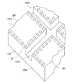
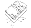
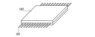
以下、本発明の実施の形態について図面を参照して詳細に説明する。始めに、図1を参照して、本発明の第1の実施の形態に係る積層チップパッケージの構成について説明する。図1は、本実施の形態に係る積層チップパッケージの斜視図である。図1に示したように、本実施の形態に係る積層チップパッケージ1は、直方体形状の本体2を備えている。本体2は、上面2a、下面2b、互いに反対側を向いた第1の側面2cおよび第2の側面2d、ならびに互いに反対側を向いた第3の側面2eおよび第4の側面2fを有している。
次に、本発明の第2の実施の形態について説明する。本実施の形態に係る積層チップパッケージ1では、本体2の4つの側面2c〜2fは、配線3が配置された少なくとも1つの第1の種類の側面と、配線3が配置されていない少なくとも1つの第2の種類の側面とを含んでいる。本実施の形態に係る積層チップパッケージ1の外観は、例えば、第1の実施の形態と同様に、図1に示したようになる。この例では、本体2の4つの側面2c〜2fのうち、側面2c,2dが第1の種類の側面であり、側面2e,2fが第2の種類の側面である。
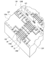
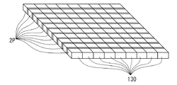
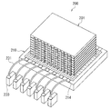
次に、本発明の第3の実施の形態について説明する。始めに、図36を参照して、本実施の形態に係る電子部品の構成について説明する。図36は、本実施の形態に係る電子部品の斜視図である。図37は、図36に示した電子部品の分解斜視図である。本実施の形態に係る電子部品は、フラッシュメモリ、DRAM、SRAM、MRAM、PROM、FeRAM等のメモリデバイスを実現するものである。
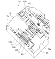
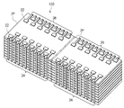
次に、図40および図41を参照して、本発明の第4の実施の形態について説明する。図40は、本実施の形態に係る積層チップパッケージの斜視図である。図41は、下面側から見た図40の積層チップパッケージを示す斜視図である。
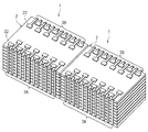
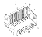
次に、図42および図43を参照して、本発明の第5の実施の形態について説明する。図42は、本実施の形態に係る電子部品の一態様を示す斜視図である。図43は、本実施の形態に係る電子部品の他の態様を示す斜視図である。本実施の形態に係る電子部品は、フラッシュメモリ、DRAM、SRAM、MRAM、PROM、FeRAM等のメモリデバイスを実現するものである。
Claims (12)
- 上面、下面および4つの側面を有する本体と、
前記本体の少なくとも1つの側面に配置された配線とを備え、
前記本体は、積層された複数の階層部分を含み、
前記複数の階層部分は、それぞれ第1の種類の半導体チップを含む複数の第1の種類の階層部分と、第2の種類の半導体チップを含む第2の種類の階層部分とを含み、
前記第1の種類の半導体チップは、複数のメモリセルを含み、
前記第2の種類の半導体チップは、前記複数の第1の種類の階層部分に含まれる複数のメモリセルに対する書き込みと読み出しを制御する回路を含み、
前記第1の種類の半導体チップと前記第2の種類の半導体チップは、いずれも、上面、下面および4つの側面を有し、
前記複数の階層部分の各々は、前記第1の種類または第2の種類の半導体チップの4つの側面のうちの少なくとも1つの側面を覆う絶縁部と、前記第1の種類または第2の種類の半導体チップに接続された複数の電極とを含み、
前記絶縁部は、前記配線が配置された前記本体の前記少なくとも1つの側面に配置された少なくとも1つの端面を有し、
前記複数の電極の各々は、前記配線が配置された前記本体の前記少なくとも1つの側面に配置され且つ前記絶縁部によって囲まれた端面を有し、
前記配線は、前記複数の階層部分における複数の電極の端面に接続されていることを特徴とする積層チップパッケージ。 - 前記第1の種類の半導体チップは、更に、そこに含まれる複数のメモリセルのみに関係する回路を含むことを特徴とする請求項1記載の積層チップパッケージ。
- 更に、前記本体の上面と下面の少なくとも一方に配置され、前記配線に接続された複数の端子を備えたことを特徴とする請求項1記載の積層チップパッケージ。
- 前記本体の4つの側面は、前記配線が配置された少なくとも1つの第1の種類の側面と、前記配線が配置されていない少なくとも1つの第2の種類の側面とを含み、
前記第1の種類または第2の種類の半導体チップの4つの側面は、前記本体の前記少なくとも1つの第1の種類の側面との間に前記絶縁部が配置された少なくとも1つの第1の種類の側面と、前記本体の前記少なくとも1つの第2の種類の側面に配置された少なくとも1つの第2の種類の側面とを含むことを特徴とする請求項1記載の積層チップパッケージ。 - 積層チップパッケージと、前記積層チップパッケージに接合された回路層とを備えた電子部品であって、
前記積層チップパッケージは、上面、下面および4つの側面を有する本体と、前記本体の少なくとも1つの側面に配置された配線とを備え、
前記本体は、積層された複数の階層部分を含み、
前記複数の階層部分の各々は、上面、下面および4つの側面を有すると共に複数のメモリセルを含む半導体チップと、前記半導体チップの4つの側面のうちの少なくとも1つの側面を覆う絶縁部と、前記半導体チップに接続された複数の電極とを含み、
前記絶縁部は、前記配線が配置された前記本体の前記少なくとも1つの側面に配置された少なくとも1つの端面を有し、
前記複数の電極の各々は、前記配線が配置された前記本体の前記少なくとも1つの側面に配置され且つ前記絶縁部によって囲まれた端面を有し、
前記配線は、前記複数の階層部分における複数の電極の端面に接続され、
前記回路層は、前記積層チップパッケージの前記配線に接続されて、前記複数の階層部分に含まれる複数のメモリセルに対する書き込みと読み出しを制御する回路を含むことを特徴とする電子部品。 - 前記半導体チップは、更に、そこに含まれる複数のメモリセルのみに関係する回路を含むことを特徴とする請求項5記載の電子部品。
- 前記積層チップパッケージは、更に、前記本体の上面と下面の少なくとも一方に配置され、前記配線に接続された複数の端子を備え、前記回路層は、前記複数の端子に接続されていることを特徴とする請求項5記載の電子部品。
- 前記本体の4つの側面は、前記配線が配置された少なくとも1つの第1の種類の側面と、前記配線が配置されていない少なくとも1つの第2の種類の側面とを含み、
前記半導体チップの4つの側面は、前記本体の前記少なくとも1つの第1の種類の側面との間に前記絶縁部が配置された少なくとも1つの第1の種類の側面と、前記本体の前記少なくとも1つの第2の種類の側面に配置された少なくとも1つの第2の種類の側面とを含むことを特徴とする請求項5記載の電子部品。 - 積層された複数の積層チップパッケージと、前記複数の積層チップパッケージのうちの1つに接合され且つ電気的に接続された回路層とを備えた電子部品であって、
上下に隣接する2つの積層チップパッケージは、互いに電気的に接続され、
前記複数の積層チップパッケージの各々は、上面、下面および4つの側面を有する本体と、前記本体の少なくとも1つの側面に配置された配線とを備え、
前記本体は、積層された複数の階層部分を含み、
前記複数の階層部分の各々は、上面、下面および4つの側面を有すると共に複数のメモリセルを含む半導体チップと、前記半導体チップの4つの側面のうちの少なくとも1つの側面を覆う絶縁部と、前記半導体チップに接続された複数の電極とを含み、
前記絶縁部は、前記配線が配置された前記本体の前記少なくとも1つの側面に配置された少なくとも1つの端面を有し、
前記複数の電極の各々は、前記配線が配置された前記本体の前記少なくとも1つの側面に配置され且つ前記絶縁部によって囲まれた端面を有し、
前記配線は、前記複数の階層部分における複数の電極の端面に接続され、
前記回路層は、複数の前記積層チップパッケージに含まれる複数のメモリセルに対する書き込みと読み出しを制御する回路を含むことを特徴とする電子部品。 - 前記半導体チップは、更に、そこに含まれる複数のメモリセルのみに関係する回路を含むことを特徴とする請求項9記載の電子部品。
- 前記複数の積層チップパッケージの各々は、更に、前記本体の上面に配置され、前記配線に接続された複数の第1の端子と、前記本体の下面に配置され、前記配線に接続された複数の第2の端子とを備え、
前記上下に隣接する2つの積層チップパッケージにおいて、下側の積層チップパッケージの複数の第1の端子と上側の積層チップパッケージの複数の第2の端子とが電気的に接続されていることを特徴とする請求項9記載の電子部品。 - 前記本体の4つの側面は、前記配線が配置された少なくとも1つの第1の種類の側面と、前記配線が配置されていない少なくとも1つの第2の種類の側面とを含み、
前記半導体チップの4つの側面は、前記本体の前記少なくとも1つの第1の種類の側面との間に前記絶縁部が配置された少なくとも1つの第1の種類の側面と、前記本体の前記少なくとも1つの第2の種類の側面に配置された少なくとも1つの第2の種類の側面とを含むことを特徴とする請求項9記載の電子部品。
Applications Claiming Priority (2)
| Application Number | Priority Date | Filing Date | Title |
|---|---|---|---|
| US12/285,101 US7557439B1 (en) | 2008-09-29 | 2008-09-29 | Layered chip package that implements memory device |
| US12/285,101 | 2008-09-29 |
Publications (2)
| Publication Number | Publication Date |
|---|---|
| JP2010087502A true JP2010087502A (ja) | 2010-04-15 |
| JP5535560B2 JP5535560B2 (ja) | 2014-07-02 |
Family
ID=40811004
Family Applications (1)
| Application Number | Title | Priority Date | Filing Date |
|---|---|---|---|
| JP2009207677A Expired - Fee Related JP5535560B2 (ja) | 2008-09-29 | 2009-09-09 | メモリデバイスを実現する積層チップパッケージ |
Country Status (2)
| Country | Link |
|---|---|
| US (1) | US7557439B1 (ja) |
| JP (1) | JP5535560B2 (ja) |
Cited By (5)
| Publication number | Priority date | Publication date | Assignee | Title |
|---|---|---|---|---|
| JP2012033861A (ja) * | 2010-08-02 | 2012-02-16 | Headway Technologies Inc | 積層半導体基板および積層チップパッケージ並びにこれらの製造方法 |
| JP2012039076A (ja) * | 2010-08-09 | 2012-02-23 | Headway Technologies Inc | 積層チップパッケージおよびその製造方法 |
| JP2012109523A (ja) * | 2010-11-18 | 2012-06-07 | Headway Technologies Inc | メモリデバイスおよび積層半導体基板並びにこれらの製造方法 |
| JP2013077767A (ja) * | 2011-09-30 | 2013-04-25 | Toshiba Corp | 半導体装置及びその製造方法、並びに半導体装置の管理システム |
| US10074667B1 (en) | 2017-03-10 | 2018-09-11 | Toshiba Memory Corporation | Semiconductor memory device |
Families Citing this family (16)
| Publication number | Priority date | Publication date | Assignee | Title |
|---|---|---|---|---|
| US7968374B2 (en) * | 2009-02-06 | 2011-06-28 | Headway Technologies, Inc. | Layered chip package with wiring on the side surfaces |
| US8274165B2 (en) * | 2009-02-10 | 2012-09-25 | Headway Technologies, Inc. | Semiconductor substrate, laminated chip package, semiconductor plate and method of manufacturing the same |
| US7915083B1 (en) * | 2009-10-28 | 2011-03-29 | Headway Technologies, Inc. | Method of manufacturing layered chip package |
| US8012802B2 (en) * | 2010-02-04 | 2011-09-06 | Headway Technologies, Inc. | Method of manufacturing layered chip package |
| TWI419197B (zh) * | 2010-04-26 | 2013-12-11 | Max Echo Technologies Corp | Production method and process adjustment method of laminated wafer |
| US8421243B2 (en) | 2010-06-24 | 2013-04-16 | Headway Technologies, Inc. | Layered chip package and method of manufacturing same |
| US8203215B2 (en) * | 2010-07-13 | 2012-06-19 | Headway Technologies, Inc. | Layered chip package and method of manufacturing same |
| US8203216B2 (en) * | 2010-07-13 | 2012-06-19 | Headway Technologies, Inc. | Layered chip package and method of manufacturing same |
| US8652877B2 (en) * | 2010-12-06 | 2014-02-18 | Headway Technologies, Inc. | Method of manufacturing layered chip package |
| US8536712B2 (en) | 2011-01-26 | 2013-09-17 | Sae Magnetics Ltd. | Memory device and method of manufacturing the same |
| JP5893287B2 (ja) * | 2011-08-10 | 2016-03-23 | ルネサスエレクトロニクス株式会社 | 半導体装置および基板 |
| US10354980B1 (en) * | 2018-03-22 | 2019-07-16 | Sandisk Technologies Llc | Three-dimensional memory device containing bonded chip assembly with through-substrate via structures and method of making the same |
| US10354987B1 (en) | 2018-03-22 | 2019-07-16 | Sandisk Technologies Llc | Three-dimensional memory device containing bonded chip assembly with through-substrate via structures and method of making the same |
| US10923456B2 (en) * | 2018-12-20 | 2021-02-16 | Cerebras Systems Inc. | Systems and methods for hierarchical exposure of an integrated circuit having multiple interconnected die |
| US10879260B2 (en) | 2019-02-28 | 2020-12-29 | Sandisk Technologies Llc | Bonded assembly of a support die and plural memory dies containing laterally shifted vertical interconnections and methods for making the same |
| KR20210128681A (ko) * | 2020-04-17 | 2021-10-27 | 에스케이하이닉스 주식회사 | 저항 소자를 구비하는 반도체 장치 |
Citations (3)
| Publication number | Priority date | Publication date | Assignee | Title |
|---|---|---|---|---|
| JPH06177318A (ja) * | 1991-09-30 | 1994-06-24 | Internatl Business Mach Corp <Ibm> | マルチチツプ集積回路パツケージ及びそのシステム |
| JPH08236688A (ja) * | 1994-12-20 | 1996-09-13 | Internatl Business Mach Corp <Ibm> | 電子モジュールおよびその形成方法 |
| JP2002110899A (ja) * | 2000-09-29 | 2002-04-12 | Toshiba Corp | 不揮発性半導体記憶装置および不揮発性半導体メモリシステム |
Family Cites Families (11)
| Publication number | Priority date | Publication date | Assignee | Title |
|---|---|---|---|---|
| US5838603A (en) | 1994-10-11 | 1998-11-17 | Matsushita Electric Industrial Co., Ltd. | Semiconductor device and method for fabricating the same, memory core chip and memory peripheral circuit chip |
| DE19626126C2 (de) * | 1996-06-28 | 1998-04-16 | Fraunhofer Ges Forschung | Verfahren zur Ausbildung einer räumlichen Chipanordnung und räumliche Chipanordung |
| US5953588A (en) | 1996-12-21 | 1999-09-14 | Irvine Sensors Corporation | Stackable layers containing encapsulated IC chips |
| US6373447B1 (en) * | 1998-12-28 | 2002-04-16 | Kawasaki Steel Corporation | On-chip antenna, and systems utilizing same |
| JP3767246B2 (ja) * | 1999-05-26 | 2006-04-19 | 富士通株式会社 | 複合モジュール及びプリント回路基板ユニット |
| US6831370B2 (en) * | 2001-07-19 | 2004-12-14 | Micron Technology, Inc. | Method of using foamed insulators in three dimensional multichip structures |
| US6734370B2 (en) | 2001-09-07 | 2004-05-11 | Irvine Sensors Corporation | Multilayer modules with flexible substrates |
| JP3880572B2 (ja) * | 2003-10-31 | 2007-02-14 | 沖電気工業株式会社 | 半導体チップ及び半導体装置 |
| US7227249B1 (en) * | 2003-12-24 | 2007-06-05 | Bridge Semiconductor Corporation | Three-dimensional stacked semiconductor package with chips on opposite sides of lead |
| US20060087013A1 (en) * | 2004-10-21 | 2006-04-27 | Etron Technology, Inc. | Stacked multiple integrated circuit die package assembly |
| JP2007036104A (ja) | 2005-07-29 | 2007-02-08 | Nec Electronics Corp | 半導体装置およびその製造方法 |
-
2008
- 2008-09-29 US US12/285,101 patent/US7557439B1/en not_active Expired - Fee Related
-
2009
- 2009-09-09 JP JP2009207677A patent/JP5535560B2/ja not_active Expired - Fee Related
Patent Citations (3)
| Publication number | Priority date | Publication date | Assignee | Title |
|---|---|---|---|---|
| JPH06177318A (ja) * | 1991-09-30 | 1994-06-24 | Internatl Business Mach Corp <Ibm> | マルチチツプ集積回路パツケージ及びそのシステム |
| JPH08236688A (ja) * | 1994-12-20 | 1996-09-13 | Internatl Business Mach Corp <Ibm> | 電子モジュールおよびその形成方法 |
| JP2002110899A (ja) * | 2000-09-29 | 2002-04-12 | Toshiba Corp | 不揮発性半導体記憶装置および不揮発性半導体メモリシステム |
Cited By (6)
| Publication number | Priority date | Publication date | Assignee | Title |
|---|---|---|---|---|
| JP2012033861A (ja) * | 2010-08-02 | 2012-02-16 | Headway Technologies Inc | 積層半導体基板および積層チップパッケージ並びにこれらの製造方法 |
| JP2012039076A (ja) * | 2010-08-09 | 2012-02-23 | Headway Technologies Inc | 積層チップパッケージおよびその製造方法 |
| US8362602B2 (en) | 2010-08-09 | 2013-01-29 | Headway Technologies, Inc. | Layered chip package and method of manufacturing same |
| JP2012109523A (ja) * | 2010-11-18 | 2012-06-07 | Headway Technologies Inc | メモリデバイスおよび積層半導体基板並びにこれらの製造方法 |
| JP2013077767A (ja) * | 2011-09-30 | 2013-04-25 | Toshiba Corp | 半導体装置及びその製造方法、並びに半導体装置の管理システム |
| US10074667B1 (en) | 2017-03-10 | 2018-09-11 | Toshiba Memory Corporation | Semiconductor memory device |
Also Published As
| Publication number | Publication date |
|---|---|
| JP5535560B2 (ja) | 2014-07-02 |
| US7557439B1 (en) | 2009-07-07 |
Similar Documents
| Publication | Publication Date | Title |
|---|---|---|
| JP5535560B2 (ja) | メモリデバイスを実現する積層チップパッケージ | |
| JP5576962B2 (ja) | 積層チップパッケージの製造方法 | |
| JP5461077B2 (ja) | 積層チップパッケージ | |
| JP5451204B2 (ja) | 積層チップパッケージの製造方法 | |
| JP5432604B2 (ja) | 積層チップパッケージの製造方法 | |
| JP5102339B2 (ja) | 積層チップパッケージの製造方法 | |
| JP5491802B2 (ja) | ヒートシンクを備えた積層チップパッケージ | |
| JP5550872B2 (ja) | 積層チップパッケージおよびその製造方法 | |
| JP5275941B2 (ja) | 積層チップパッケージおよびその製造方法 | |
| JP5154667B2 (ja) | 積層チップパッケージおよびその製造方法 | |
| JP5004311B2 (ja) | 積層チップパッケージおよびその製造方法 | |
| JP4927195B2 (ja) | 複合型積層チップパッケージおよびその製造方法 | |
| JP4927194B2 (ja) | 積層チップパッケージの製造方法 | |
| JP5228068B2 (ja) | 積層チップパッケージおよびその製造方法 | |
| JP4948635B2 (ja) | 積層チップパッケージの製造方法 | |
| JP5653949B2 (ja) | 積層チップパッケージの製造方法 |
Legal Events
| Date | Code | Title | Description |
|---|---|---|---|
| A621 | Written request for application examination |
Free format text: JAPANESE INTERMEDIATE CODE: A621 Effective date: 20120510 |
|
| A977 | Report on retrieval |
Free format text: JAPANESE INTERMEDIATE CODE: A971007 Effective date: 20130522 |
|
| A131 | Notification of reasons for refusal |
Free format text: JAPANESE INTERMEDIATE CODE: A131 Effective date: 20130604 |
|
| A521 | Request for written amendment filed |
Free format text: JAPANESE INTERMEDIATE CODE: A523 Effective date: 20130828 |
|
| TRDD | Decision of grant or rejection written | ||
| A01 | Written decision to grant a patent or to grant a registration (utility model) |
Free format text: JAPANESE INTERMEDIATE CODE: A01 Effective date: 20140422 |
|
| A61 | First payment of annual fees (during grant procedure) |
Free format text: JAPANESE INTERMEDIATE CODE: A61 Effective date: 20140423 |
|
| R150 | Certificate of patent or registration of utility model |
Ref document number: 5535560 Country of ref document: JP Free format text: JAPANESE INTERMEDIATE CODE: R150 |
|
| R250 | Receipt of annual fees |
Free format text: JAPANESE INTERMEDIATE CODE: R250 |
|
| R250 | Receipt of annual fees |
Free format text: JAPANESE INTERMEDIATE CODE: R250 |
|
| R250 | Receipt of annual fees |
Free format text: JAPANESE INTERMEDIATE CODE: R250 |
|
| LAPS | Cancellation because of no payment of annual fees |