JP2010080486A - Multilayer wiring board, probe card, and method of manufacturing multilayer wiring board - Google Patents
Multilayer wiring board, probe card, and method of manufacturing multilayer wiring board Download PDFInfo
- Publication number
- JP2010080486A JP2010080486A JP2008243940A JP2008243940A JP2010080486A JP 2010080486 A JP2010080486 A JP 2010080486A JP 2008243940 A JP2008243940 A JP 2008243940A JP 2008243940 A JP2008243940 A JP 2008243940A JP 2010080486 A JP2010080486 A JP 2010080486A
- Authority
- JP
- Japan
- Prior art keywords
- multilayer wiring
- wiring board
- heater
- core base
- insulating layer
- Prior art date
- Legal status (The legal status is an assumption and is not a legal conclusion. Google has not performed a legal analysis and makes no representation as to the accuracy of the status listed.)
- Granted
Links
Images


Abstract
Description
本発明は多層配線基板、プローブカード、及び、多層配線基板の製造方法に関するものであり、例えば、ヒータを内臓した多層配線基板の熱膨張率を低減するための構成に関する。 The present invention relates to a multilayer wiring board, a probe card, and a method for manufacturing the multilayer wiring board, and, for example, relates to a configuration for reducing the coefficient of thermal expansion of a multilayer wiring board with a built-in heater.
近年、電子機器の高性能化、小型化が急速に進展している。これに伴い、電子機器を構成する半導体素子、及び半導体素子を実装するための配線基板には、小型薄型であること、高い性能を有すること、高い信頼性を有すること等が要求されている。このような要求に応えるべく、半導体素子の実装方法としては、プリント基板等の配線基板上に半導体素子を直接実装するベアチップ実装技術が用いられている。 In recent years, high performance and miniaturization of electronic devices are rapidly progressing. Along with this, a semiconductor element constituting an electronic device and a wiring board for mounting the semiconductor element are required to be small and thin, to have high performance, and to have high reliability. In order to meet such demands, a bare chip mounting technique in which a semiconductor element is directly mounted on a wiring board such as a printed board is used as a method for mounting a semiconductor element.
また、半導体素子の多ピン化に伴い、半導体素子を実装するための配線基板として、配線層を多層化した多層配線基板の重要性が高まっている。また、半導体素子をテストするためのテスターボードにおいても、配線層の多層化は必要不可欠なものとなっている。 Further, with the increase in the number of pins of semiconductor elements, the importance of multilayer wiring boards in which wiring layers are multilayered is increasing as a wiring board for mounting semiconductor elements. Also, in a tester board for testing a semiconductor element, the multilayer wiring layer is indispensable.
このような多層配線基板としては、例えば、絶縁層と導体層とが交互に積層された配線形成層がコア基板の片面又は両面に形成されたビルトアップ方式のものが用いられている。 As such a multilayer wiring board, for example, a built-up type board in which a wiring forming layer in which insulating layers and conductor layers are alternately laminated is formed on one side or both sides of a core substrate is used.
ところで、ウェーハレベルテストにおいては、シリコンの熱膨張係数は約3.5ppm/℃であるのに対し、プローブカードとなるガラスエポキシ樹脂基板の熱膨張係数は12〜20ppm/℃である、このように、シリコンウェーハとガラスエポキシ樹脂基板の熱膨張係数は大きく異なっているため、シリコンウェーハの熱膨張率に近似させたプローブカードが必要となる。 By the way, in the wafer level test, the thermal expansion coefficient of silicon is about 3.5 ppm / ° C., whereas the thermal expansion coefficient of the glass epoxy resin substrate to be a probe card is 12 to 20 ppm / ° C. Since the thermal expansion coefficients of the silicon wafer and the glass epoxy resin substrate are greatly different, a probe card that approximates the thermal expansion coefficient of the silicon wafer is required.
実装基板の熱膨張係数を低減する手法としては、低熱膨張率の金属であるインバー等をコアとして用いるメタルコア基板や、ガラスエポキシ樹脂基板の基材として用いられるガラス布に代えて、熱膨張係数が1.0ppm/℃以下であるカーボンファイバを用いる手法がある。 As a method of reducing the thermal expansion coefficient of the mounting substrate, instead of a metal core substrate using a metal having a low thermal expansion coefficient such as Invar as a core or a glass cloth used as a base material of a glass epoxy resin substrate, a thermal expansion coefficient is used. There is a method using a carbon fiber of 1.0 ppm / ° C. or less.
これらの実装基板においては、低熱膨張率材料が配線層の熱膨張を抑制できる構造であれば効果が大きい。しかしながら、ウェーハを試験する場合は加熱することが多く、85〜125℃、場合によっては150〜200℃での試験がある。 In these mounting substrates, the effect is great if the low thermal expansion coefficient material can suppress the thermal expansion of the wiring layer. However, when testing a wafer, it is often heated and there is a test at 85-125 ° C, and sometimes 150-200 ° C.
一般的には、プローバのウェーハチャックが加熱源となるため、プローブカードはウェーハからの輻射熱で加熱される。このような構成から、プローブカードは片面加熱によって基板の表裏温度差が生じ、反りを発生させる。この反りは基板表裏温度差が緩和するまで反り挙動が安定せず、試験時のプローブのコンタクトにも影響するため、すぐに試験開始できない。 Generally, since the probe chuck of the prober serves as a heating source, the probe card is heated by radiant heat from the wafer. With such a configuration, the probe card is warped due to a temperature difference between the front and back surfaces of the substrate caused by single-sided heating. Since this warpage does not stabilize the warpage behavior until the temperature difference between the front and back surfaces of the substrate is relaxed and affects the contact of the probe during the test, the test cannot be started immediately.
このため、実装基板にヒータを取り付け、実装基板自体も加熱させて挙動を安定させることが行われている(例えば、特許文献1乃至特許文献4参照)。実装基板にヒータを取り付ける場合、最も望ましいのは実装基板の内部であり、中心付近のレイヤに内蔵させることが望ましい。実装基板のプローブ側や裏面側には充分なスペースを確保するには制約があるためである。
For this reason, a heater is attached to the mounting substrate, and the mounting substrate itself is also heated to stabilize the behavior (for example, see
一般的に、ヒータといえば、ニクロム線やステンレス線を抵抗体として蛇行配線したもの、抵抗金属箔を印刷したもの、ならびに導電性カーボンを合成ゴムに練り込んだものなどが挙げられる。
しかし、これらのヒータは発熱の安定性を求めるため、単体ではなく、金属線と複合させて用いることが多く、ヒータの熱膨張率はほぼ金属の物性と同様なものになっている。このようなヒータを基板に内蔵した場合、基板全体の熱膨張率が大きい方向に振れるため、望ましい内蔵ヒータとはならない。 However, these heaters are often used in combination with a metal wire rather than a single element in order to obtain stability of heat generation, and the thermal expansion coefficient of the heater is almost the same as the physical properties of metal. When such a heater is built in the substrate, it does not become a desirable built-in heater because the thermal expansion coefficient of the entire substrate swings in a large direction.
したがって、本発明は、熱膨張率を低減したままヒータを多層配線基板に内蔵することを目的とする。 Accordingly, an object of the present invention is to incorporate a heater in a multilayer wiring board while reducing the coefficient of thermal expansion.
本発明の一観点からは、カーボン材料からなるヒータと平板状の導電性を有する材料とを含むコア基材と、前記コア基材の表面に絶縁層と前記絶縁層に形成された導体層からなる多層配線構造を少なくとも有するとともに、前記コア基材に複数の貫通孔が設けられていることを特徴とする多層配線基板が提供される。 From one aspect of the present invention, a core base material including a heater made of a carbon material and a flat conductive material, an insulating layer on the surface of the core base material, and a conductor layer formed on the insulating layer. There is provided a multilayer wiring board having at least a multilayer wiring structure and having a plurality of through holes in the core base material.
また、本発明の別の観点からは、上記の多層配線基板の一方の面に探針と、前記探針を支持するカイド部材を設けたことを特徴とするプローブカードが提供される。 According to another aspect of the present invention, there is provided a probe card characterized in that a probe and a guide member for supporting the probe are provided on one surface of the multilayer wiring board.
さらに、別の観点からは、貫通孔が形成された平板状の導電性を有する材料とヒータ層とを積層してコア基材を形成する工程と、前記コア基材の表面に絶縁層と前記絶縁層に形成された導体層からなる多層配線構造を形成する工程とを有することを特徴とする多層配線基板の製造方法が提供される。 Furthermore, from another viewpoint, a step of forming a core base material by laminating a flat plate-like conductive material having a through hole and a heater layer, and an insulating layer on the surface of the core base material And a step of forming a multilayer wiring structure comprising a conductor layer formed on an insulating layer.
開示の多層配線基板、プローブカード、及び、多層配線基板の製造方法によれば、多層配線基板温度をSiの温度に近接させることによって、Siと実装基板の温度差を無くし、Siから熱の影響を受けずに、多層配線基板自身の温度勾配や温度変化を低減できる。 According to the disclosed multilayer wiring board, probe card, and multilayer wiring board manufacturing method, the temperature difference between Si and the mounting board is eliminated by bringing the multilayer wiring board temperature close to the temperature of Si, and the influence of heat from Si. The temperature gradient and the temperature change of the multilayer wiring board itself can be reduced without receiving.
また、それによって、多層配線基板の反り等を防ぐことができるため、コンタクトエラーを低減させることができる。また、複合させたヒータ層も低熱膨張率であることから、多層配線基板全体の熱膨張率を大きくすることなくヒータを内蔵させることができる。 Further, it is possible to prevent the multilayer wiring board from warping and the like, so that contact errors can be reduced. Further, since the combined heater layer also has a low coefficient of thermal expansion, it is possible to incorporate the heater without increasing the coefficient of thermal expansion of the entire multilayer wiring board.
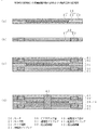
ここで、図1を参照して、本発明の実施の形態のプローブカードを説明する。
図1は本発明の実施の形態のプローブカードの概念的構成図であり、ヒータ2と低熱膨張率コア層3を積層させて導電性コア基材1を構成する。この場合、ヒータ2の両面を低熱膨張率コア層3で挟んでも良いし、或いは、低熱膨張率コア層3の両面をヒータ2で挟んでも良い。
Here, with reference to FIG. 1, the probe card of embodiment of this invention is demonstrated.
FIG. 1 is a conceptual configuration diagram of a probe card according to an embodiment of the present invention, in which a
この場合のヒータ2を構成するヒータ層は、カーボンナノチューブ、カーボン短繊維、或いは、カーボン長繊維の少なくとも一つを含むものであり、低熱膨張率のヒータ層を構成する。なお、カーボン長繊維とは、カーボン繊維が絡み合って一体になったものであり、カーボン単繊維とは、カーボン繊維が絡み合わずにバラバラな状態なっているものである。また、ヒータ層の両端にはヒータ電極7、特に、一方向性炭素繊維を用いたヒータ電極7を設けることが望ましい。
The heater layer constituting the
また、低熱膨張率コア層3は、カーボン繊維を平織りにした織布にエポキシ樹脂を含浸させたプリプレグ、即ち、CFRP(炭素繊維強化樹脂)、インバー、コバール、或いは、42アロイの少なくとも1つを含むものであり、熱膨張率が6ppm/℃以下の性質を持ち、いずれも導電性を有するので導電性コア層となる。したがって、ヒータ2と積層する場合には、ヒータ2との間に絶縁層、例えば、ガラス/エポキシプリプレグ等の絶縁性プリプレグを設ける必要がある。なお、低熱膨張率コア層3に用いられるエポキシ系樹脂組成物には、アルミナフィラー、窒化アルミニウムフィラー、シリカフィラー等の無機フィラーが混合され熱膨張率が低減されている。
The low thermal expansion
このヒータ2と低熱膨張率コア層3を積層させて導電性コア基材1の表面に、信号用、電源用、或いは、グラウンド用の配線パターン6を形成した樹脂絶縁層5からなる配線形成層4を所定の層数だけ積層することによって多層配線基板を構成する。また、多層配線基板にスルーホールを設けて導電性部材で埋め込むことによって、ヒータ電極7と電気的に接続するスルービア8を形成する。なお、ヒータ電極7として一方向性炭素繊維を用いた場合には、一方向性繊維層は、繊維方向には高い導電性を示すが、繊維と垂直方向では高導電性を示さない。
A wiring forming layer comprising a
このようなスルービア8は、配線レイアウト等に応じて所定の数のスルーホールが形成されており、このスルーホールには導電性コア基材1と絶縁するためのクリアランスホールが形成され、それぞれのクリアランスホールには絶縁樹脂が充填されて埋込絶縁層9を形成している。この場合のクリアランスホールの直径は、例えば0.8mmとし、クリアランスホールを貫通するスルーホールの直径を0.3mmとする。
In such a through via 8, a predetermined number of through holes are formed according to the wiring layout and the like, and clearance holes for insulating from the
また、配線形成層4に形成された配線パターン6は、スルーホールの内壁面に形成されたスルービアにより電気的に接続されている。また、配線形成層4と導電性コア基材1との間は絶縁層10、例えば、ガラス/エポキシプリプレグ等の絶縁性プリプレグにより絶縁されている。
Further, the
この多層配線基板の一方の面に探針となるカンチレバー11と、カンチレバー11を支持するガイド12を設ける。多層配線基板の他方の面には、コンデンサ等の受動素子、スティフナー、或いは、ポゴ基板に対する接続端子等の裏面部品13を設けることによって、プローブカードの基本構成が得られる。
A
加熱されたSiウェーハ等の半導体ウェーハ15の試験時において、プローブカードの基板部分の温度が、半導体の温度と同等になるように、スルービア8を介してヒータ2に通電することによって加熱する。この場合、導電性コア基材1を構成するヒータ2、ヒータ電極7、及び、低熱膨張率コア層3の全てが低熱膨張率であるのでSi等の半導体の熱膨張率に近似させることができる。なお、図における符号14は半導体ウェーハ15を保持するステージである。
During the test of the semiconductor wafer 15 such as a heated Si wafer, heating is performed by energizing the
このように、本発明においては導電性コア基材の低熱膨張率化とともに、ヒータ層の低熱膨張率化を図ることにより、低熱膨張率化を実現しながら基板そのものを加熱できるため、より被試験半導体の熱膨張率に近似させながら、反り挙動も安定した多層配線基板を実現することができる。 Thus, in the present invention, by reducing the thermal expansion coefficient of the conductive core base material and reducing the thermal expansion coefficient of the heater layer, the substrate itself can be heated while realizing a low thermal expansion coefficient. A multilayer wiring board having a stable warping behavior while approximating the thermal expansion coefficient of the semiconductor can be realized.
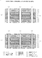
以上を前提として、次に、図2乃至図4を参照して本発明の実施例1の多層配線基板の製造工程を説明する。まず、図2(a)に示すように、ヒータ材料として、エポキシ樹脂中にカーボンナノチューブを例えば10vol%分散させた厚さが、例えば、0.1mmのヒータ層21とのその両端に設けた一方向性炭素繊維からなるヒータ電極22とをガラス/エポキシプリプレグからなる絶縁性プリプレグ23で挟んでヒータ20を構成する。
Based on the above, the manufacturing process of the multilayer wiring board according to the first embodiment of the present invention will be described next with reference to FIGS. First, as shown in FIG. 2 (a), as a heater material, for example, a carbon nanotube dispersed in an epoxy resin, for example, 10 vol% in thickness is provided at both ends of a
次いで、図2(b)に示すように、厚さが、例えば、0.2mmのカーボンファイバ織布とエポキシ系樹脂組成物とを複合化してなる導電性プリプレグ31を例えば3枚積層したのち、ドリル加工によりヒータ電極22に対するスルービアのためのクリアランスホールを形成する。このクリアランスホールの直径は例えば、0.8mmであり、この内部をエポキシ樹脂等で埋め込んで埋込絶縁層32としてCFRPコア層30を構成する。なお、導電性プリプレグ31を構成するエポキシ系樹脂組成物には、例えば、組成物全体の10wt%のシリカフィラーを混合した。
Next, as shown in FIG. 2B, for example, after laminating, for example, three
次いで、図2(c)に示すように、一枚のヒータ20の両側にCFRPコア層30を積層するとともに、CFRPコア層30の両側に厚さが、例えば、0.1mmのガラス/エポキシプリプレグからなる絶縁性プリプレグ41を積層したのち圧着して、例えば、全体の厚さを約1.7mmとする。
Next, as shown in FIG. 2C, a
次いで、図2(d)に示すように、ドリル加工により後工程で積層する多層配線構造を構成する信号配線、電源配線、或いは、グラウンド配線に対するスルービアのためのクリアランスホールを例えば、約5000個形成する。このクリアランスホールの直径は例えば、1.0mmであり、この内部をエポキシ樹脂等で埋め込んで埋込絶縁層42として導電性コア基材40が得られる。
Next, as shown in FIG. 2 (d), for example, about 5000 clearance holes are formed for through vias for signal wiring, power supply wiring, or ground wiring constituting a multilayer wiring structure to be laminated in a later process by drilling. To do. The clearance hole has a diameter of, for example, 1.0 mm. The inside of the clearance hole is filled with an epoxy resin or the like, and the
次いで、図3(e)に示すように、厚さが、例えば、100μmのガラスエポキシ樹脂からなる樹脂絶縁層51の両面に厚さが、例えば、35μmの銅箔を貼り付けた両面板を用い、ドライフィルムレジスト(図示は省略)でパターニング後、ウェットエッチングにより銅箔パターン52を形成して配線形成層50を形成する。なお、銅箔パターン52はその積層位置に応じて信号配線、電源配線、或いは、グラウンド配線を構成する。
Next, as shown in FIG. 3E, a double-sided board in which a copper foil with a thickness of 35 μm, for example, is attached to both surfaces of a
次いで、信号配線、電源配線、或いは、グラウンド配線を設けた配線形成層50を、厚さが、例えば、0.1mmのガラス/エポキシプリプレグからなる絶縁性プリプレグ53を介して導電性コア基材40の両面に必要とする層数分レイアップする。
Next, the
次いで、図3(f)に示すように、レイアップした積層物を金型にセットし、例えば、185℃に加熱した状態で真空プレスによって一体化積層を行った。 Next, as shown in FIG. 3 (f), the laid-up laminate was set in a mold, and integrated lamination was performed by, for example, a vacuum press while being heated to 185 ° C.
次いで、図4(g)に示すように、一体化積層した基板に対してドリル加工により埋込絶縁層32,42に対する位置にスルーホール54を形成する。この場合、埋込絶縁層32に対するスルーホール54の直径は0.3mmとし、埋込絶縁層42に対するスルーホール54の直径は0.3mmとする。
Next, as shown in FIG. 4G, a through
次いで、図4(h)に示すように、デスミア処理、無電解銅めっき、電解銅めっきを順次行うことによってスルーホール54を銅で埋め込む。次いで、ドライフィルムレジスト(図示は省略)でパターニングを行いエッチングする、所謂テンティング法によって、表面パターンを形成するともに、配線用スルービア55及びヒータ用スルービア56を形成する。最後に、ソルダーレジスト(図示は省略)を両面に形成することによって多層配線基板を完成させた。
Next, as shown in FIG. 4H, the through
以降は、図1の示したのと同様に、この多層配線基板の一方の面に探針となるカンチレバーと、カンチレバーを支持するガイドを設ける。また、多層配線基板の他方の面には、コンデンサ等の受動素子、スティフナー、或いは、ポゴ基板に対する接続端子等の裏面部品を設けることによって、プローブカードが完成することになる。 Thereafter, as shown in FIG. 1, a cantilever that serves as a probe and a guide that supports the cantilever are provided on one surface of the multilayer wiring board. In addition, a probe card is completed by providing a back surface component such as a passive element such as a capacitor, a stiffener, or a connection terminal for the pogo substrate on the other surface of the multilayer wiring board.
本発明の実施例1においては、導電性コア基材40を構成する各種材料を低熱膨張率の材料を用いて構成しているので、この導電性コア基材40は、温度範囲20〜200℃において、面方向の平均熱膨張率が2ppm/℃で、Siの熱膨張係数(約3.5ppm/℃)に近い値となる。なお、厚さ方向の平均熱膨張率が80ppm/℃であった。
In Example 1 of the present invention, since the various materials constituting the conductive
次に、図5乃至図7を参照して本発明の実施例2の多層配線基板の製造工程を説明する。まず、図5(a)に示すように、実施例1と同様に、ヒータ材料として、エポキシ樹脂中にカーボンナノチューブを例えば10vol%分散させた厚さが、例えば、0.1mmのヒータ層21とのその両端に設けた一方向性炭素繊維からなるヒータ電極22とをガラス/エポキシプリプレグからなる絶縁性プリプレグ23で挟んでヒータ20を構成する。
Next, the manufacturing process of the multilayer wiring board according to the second embodiment of the present invention will be described with reference to FIGS. First, as shown in FIG. 5A, similar to Example 1, as a heater material, for example, a
次いで、図5(b)に示すように、厚さが、例えば、0.2mmのカーボンファイバ織布とエポキシ系樹脂組成物とを複合化してなる導電性プリプレグ61を積層したのち、ドリル加工によりヒータ電極22に対するスルービアのためのクリアランスホールを形成する。このクリアランスホールの直径は例えば、0.8mmであり、この内部をエポキシ樹脂等で埋め込んで埋込絶縁層62としてCFRPコア層60を構成する。なお、導電性プリプレグ61を構成するエポキシ系樹脂組成物には、例えば、組成物全体の10wt%のシリカフィラーを混合した。
Next, as shown in FIG. 5B, after laminating a
次いで、図5(c)に示すように、一枚のCFRPコア層60の両側にヒータ20を積層したのち圧着する。
Next, as shown in FIG. 5 (c), the
次いで、図5(d)に示すように、ドリル加工により後工程で積層する多層配線構造を構成する信号配線、電源配線、或いは、グラウンド配線に対するスルービアのためのクリアランスホールを例えば、約5000個形成する。このクリアランスホールの直径は例えば、1.0mmであり、この内部をエポキシ樹脂等で埋め込んで埋込絶縁層71として導電性コア基材70が得られる。
Next, as shown in FIG. 5 (d), for example, about 5000 clearance holes are formed for through vias for signal wiring, power supply wiring, or ground wiring constituting a multilayer wiring structure to be laminated in a later process by drilling. To do. The clearance hole has a diameter of, for example, 1.0 mm. The inside of the clearance hole is filled with an epoxy resin or the like, and the conductive
次いで、図6(e)に示すように、厚さが、例えば、100μmのガラスエポキシ樹脂からなる樹脂絶縁層51の両面に厚さが、例えば、35μmの銅箔を貼り付けた両面板を用い、ドライフィルムレジスト(図示は省略)でパターニング後、ウェットエッチングにより銅箔パターン52を形成して配線形成層50を形成する。なお、銅箔パターン52はその積層位置に応じて信号配線、電源配線、或いは、グラウンド配線を構成する。
Next, as shown in FIG. 6E, a double-sided board in which a copper foil having a thickness of 35 μm, for example, is attached to both surfaces of a
次いで、信号配線、電源配線、或いは、グラウンド配線を設けた配線形成層50を、厚さが、例えば、0.1mmのガラス/エポキシプリプレグからなる絶縁性プリプレグ53を介して導電性コア基材70の両面に必要とする層数分レイアップする。
Next, the
次いで、図6(f)に示すように、レイアップした積層物を金型にセットし、例えば、185℃に加熱した状態で真空プレスによって一体化積層を行った。 Next, as shown in FIG. 6F, the laid-up laminate was set in a mold and, for example, integrated lamination was performed by a vacuum press while being heated to 185 ° C.
次いで、図7(g)に示すように、一体化積層した基板に対してドリル加工により埋込絶縁層62,72に対する位置にスルーホール54を形成する。この場合、埋込絶縁層62に対するスルーホール54の直径は0.3mmとし、埋込絶縁層71に対するスルーホール54の直径は0.3mmとする。
Next, as shown in FIG. 7G, a through
次いで、図7(h)に示すように、デスミア処理、無電解銅めっき、電解銅めっきを順次行うことによってスルーホール54を銅で埋め込む。次いで、ドライフィルムレジスト(図示は省略)でパターニングを行いエッチングする、所謂テンティング法によって、表面パターンを形成するともに、配線用スルービア55及びヒータ用スルービア56を形成する。最後に、ソルダーレジスト(図示は省略)を両面に形成することによって多層配線基板を完成させた。
Next, as shown in FIG. 7H, the through-
以降は、図1の示したのと同様に、この多層配線基板の一方の面に探針となるカンチレバーと、カンチレバーを支持するガイドを設ける。また、多層配線基板の他方の面には、コンデンサ等の受動素子、スティフナー、或いは、ポゴ基板に対する接続端子等の裏面部品を設けることによって、プローブカードが完成することになる。 Thereafter, as shown in FIG. 1, a cantilever that serves as a probe and a guide that supports the cantilever are provided on one surface of the multilayer wiring board. In addition, a probe card is completed by providing a back surface component such as a passive element such as a capacitor, a stiffener, or a connection terminal for the pogo substrate on the other surface of the multilayer wiring board.
本発明の実施例2においても、導電性コア基材70を構成する各種材料を低熱膨張率の材料を用いて構成しているので、この導電性コア基材70のをSiの熱膨張係数に近い値とすることができる。
Also in Example 2 of the present invention, various materials constituting the conductive
また、本発明の実施例2においては、CFRPコア層を中間にして2つのヒータを設けているので、大きな発熱量が必要な場合に有効になる。なお、図においては、上下のヒータに対して同じスルービアにより電力を供給しているが、ヒータ電極に予め互いに位置のずれた埋込絶縁層を設けたクリアランスホールを設けておき、2つのヒータに対して独立に電力を供給することができる。この場合、2つのヒータに対して独立に電力を供給することにより多層配線基板の反りを精度良く矯正することができる。 In the second embodiment of the present invention, the two heaters are provided with the CFRP core layer in the middle, which is effective when a large amount of heat generation is required. In the figure, power is supplied to the upper and lower heaters through the same through via. However, the heater electrodes are provided with clearance holes provided with buried insulating layers that are displaced from each other in advance. In contrast, power can be supplied independently. In this case, the warp of the multilayer wiring board can be accurately corrected by supplying power independently to the two heaters.
1 導電性コア基材
2 ヒータ
3 低熱膨張率コア層
4 配線形成層
5 樹脂絶縁層
6 配線パターン
7 ヒータ電極
8 スルービア
9 埋込絶縁層
10 絶縁層
11 カンチレバー
12 ガイド
13 裏面部品
14 ステージ
15 半導体ウェーハ
20 ヒータ
21 ヒータ層
22 ヒータ電極
23 絶縁性プリプレグ
30 CFRPコア層
31 導電性プリプレグ
32 埋込絶縁層
40 導電性コア基材
41 絶縁性プリプレグ
42 埋込絶縁層
50 配線形成層
51 樹脂絶縁層
52 銅箔パターン
53 絶縁性プリプレグ
54 スルーホール
55 配線用スルービア
56 ヒータ用スルービア
60 CFRPコア層
61 導電性プリプレグ
62 埋込絶縁層
70 導電性コア基材
71 埋込絶縁層
DESCRIPTION OF
Claims (7)
前記コア基材の表面に絶縁層と前記絶縁層に形成された導体層からなる多層配線構造を少なくとも有するとともに、
前記コア基材に複数の貫通孔が設けられていることを特徴とする多層配線基板。 A core base material including a heater made of a carbon material and a flat conductive material;
While having at least a multilayer wiring structure consisting of an insulating layer and a conductor layer formed on the insulating layer on the surface of the core substrate,
A multilayer wiring board comprising a plurality of through holes provided in the core base material.
探針と、前記探針を支持するカイド部材を
設けたことを特徴とするプローブカード。 At least a multi-layer wiring structure comprising a core base material including a heater made of a carbon material and a flat conductive material, and an insulating layer and a conductor layer formed on the insulating layer on the surface of the core base material , On one surface of the multilayer wiring board provided with a plurality of through holes in the core base material,
A probe card comprising a probe and a guide member that supports the probe.
前記コア基材の表面に絶縁層と前記絶縁層に形成された導体層からなる多層配線構造を形成する工程と
を有することを特徴とする多層配線基板の製造方法。 A step of forming a core base material by laminating a flat conductive material having a through hole and a heater layer;
Forming a multilayer wiring structure comprising an insulating layer and a conductor layer formed on the insulating layer on a surface of the core base material.
Priority Applications (1)
| Application Number | Priority Date | Filing Date | Title |
|---|---|---|---|
| JP2008243940A JP5251395B2 (en) | 2008-09-24 | 2008-09-24 | Multilayer wiring board, probe card, and method for manufacturing multilayer wiring board |
Applications Claiming Priority (1)
| Application Number | Priority Date | Filing Date | Title |
|---|---|---|---|
| JP2008243940A JP5251395B2 (en) | 2008-09-24 | 2008-09-24 | Multilayer wiring board, probe card, and method for manufacturing multilayer wiring board |
Publications (2)
| Publication Number | Publication Date |
|---|---|
| JP2010080486A true JP2010080486A (en) | 2010-04-08 |
| JP5251395B2 JP5251395B2 (en) | 2013-07-31 |
Family
ID=42210635
Family Applications (1)
| Application Number | Title | Priority Date | Filing Date |
|---|---|---|---|
| JP2008243940A Expired - Fee Related JP5251395B2 (en) | 2008-09-24 | 2008-09-24 | Multilayer wiring board, probe card, and method for manufacturing multilayer wiring board |
Country Status (1)
| Country | Link |
|---|---|
| JP (1) | JP5251395B2 (en) |
Cited By (6)
| Publication number | Priority date | Publication date | Assignee | Title |
|---|---|---|---|---|
| JP2010151497A (en) * | 2008-12-24 | 2010-07-08 | Micronics Japan Co Ltd | Probe card |
| WO2012111503A1 (en) * | 2011-02-16 | 2012-08-23 | 三菱重工業株式会社 | Carbon-fiber-reinforced plastic structure |
| KR101207700B1 (en) | 2010-07-28 | 2012-12-03 | 후지쯔 가부시끼가이샤 | Printed wiring board, method for manufacturing the same, and electronic equipment |
| JP2014089089A (en) * | 2012-10-30 | 2014-05-15 | Micronics Japan Co Ltd | Multilayer wiring board, and probe card using the same |
| JP2017220454A (en) * | 2016-06-03 | 2017-12-14 | ツィンファ ユニバーシティ | Manufacturing method and manufacturing installation of organic light-emitting diode |
| WO2024014610A1 (en) * | 2022-07-12 | 2024-01-18 | (주) 마이크로사이언스 | Method for manufacturing circuit board for probe card using graphene |
Citations (7)
| Publication number | Priority date | Publication date | Assignee | Title |
|---|---|---|---|---|
| JPH01174989U (en) * | 1988-05-31 | 1989-12-13 | ||
| JPH0812457A (en) * | 1994-06-28 | 1996-01-16 | Tonen Corp | Carbon fiber-reinforced carbon composite material and its production |
| JP2000346875A (en) * | 1999-06-07 | 2000-12-15 | Advantest Corp | Probe card and ic testing device using it |
| JP2001228171A (en) * | 2000-02-18 | 2001-08-24 | Japan Electronic Materials Corp | Probe card |
| JP2002249377A (en) * | 2001-02-16 | 2002-09-06 | Ibiden Co Ltd | Ceramic substrate for manufacturing and inspection equipment of semiconductor |
| JP2004087856A (en) * | 2002-08-27 | 2004-03-18 | Fujitsu Ltd | Multilayer wiring board |
| JP2004241405A (en) * | 2003-02-03 | 2004-08-26 | Denso Corp | Structure for mounting electronic component heat insulating element on printed wiring board |
-
2008
- 2008-09-24 JP JP2008243940A patent/JP5251395B2/en not_active Expired - Fee Related
Patent Citations (7)
| Publication number | Priority date | Publication date | Assignee | Title |
|---|---|---|---|---|
| JPH01174989U (en) * | 1988-05-31 | 1989-12-13 | ||
| JPH0812457A (en) * | 1994-06-28 | 1996-01-16 | Tonen Corp | Carbon fiber-reinforced carbon composite material and its production |
| JP2000346875A (en) * | 1999-06-07 | 2000-12-15 | Advantest Corp | Probe card and ic testing device using it |
| JP2001228171A (en) * | 2000-02-18 | 2001-08-24 | Japan Electronic Materials Corp | Probe card |
| JP2002249377A (en) * | 2001-02-16 | 2002-09-06 | Ibiden Co Ltd | Ceramic substrate for manufacturing and inspection equipment of semiconductor |
| JP2004087856A (en) * | 2002-08-27 | 2004-03-18 | Fujitsu Ltd | Multilayer wiring board |
| JP2004241405A (en) * | 2003-02-03 | 2004-08-26 | Denso Corp | Structure for mounting electronic component heat insulating element on printed wiring board |
Cited By (8)
| Publication number | Priority date | Publication date | Assignee | Title |
|---|---|---|---|---|
| JP2010151497A (en) * | 2008-12-24 | 2010-07-08 | Micronics Japan Co Ltd | Probe card |
| KR101207700B1 (en) | 2010-07-28 | 2012-12-03 | 후지쯔 가부시끼가이샤 | Printed wiring board, method for manufacturing the same, and electronic equipment |
| WO2012111503A1 (en) * | 2011-02-16 | 2012-08-23 | 三菱重工業株式会社 | Carbon-fiber-reinforced plastic structure |
| JP2012169533A (en) * | 2011-02-16 | 2012-09-06 | Mitsubishi Heavy Ind Ltd | Carbon fiber-reinforced plastic structure |
| US10357938B2 (en) | 2011-02-16 | 2019-07-23 | Mitsubishi Heavy Industries, Ltd. | Carbon-fiber-reinforced plastic structure |
| JP2014089089A (en) * | 2012-10-30 | 2014-05-15 | Micronics Japan Co Ltd | Multilayer wiring board, and probe card using the same |
| JP2017220454A (en) * | 2016-06-03 | 2017-12-14 | ツィンファ ユニバーシティ | Manufacturing method and manufacturing installation of organic light-emitting diode |
| WO2024014610A1 (en) * | 2022-07-12 | 2024-01-18 | (주) 마이크로사이언스 | Method for manufacturing circuit board for probe card using graphene |
Also Published As
| Publication number | Publication date |
|---|---|
| JP5251395B2 (en) | 2013-07-31 |
Similar Documents
| Publication | Publication Date | Title |
|---|---|---|
| JP4855753B2 (en) | Multilayer wiring board and manufacturing method thereof | |
| US8119925B2 (en) | Core substrate and printed wiring board | |
| US7002080B2 (en) | Multilayer wiring board | |
| CN102090155B (en) | Method for integrating at least one electronic component into a printed circuit board, and printed circuit board | |
| US9538642B2 (en) | Wiring board and method for manufacturing the same | |
| JP5251395B2 (en) | Multilayer wiring board, probe card, and method for manufacturing multilayer wiring board | |
| US20100163290A1 (en) | Printed wiring board and method for manufacturing the same | |
| JP2009290124A (en) | Printed wiring board | |
| US8878076B2 (en) | Wiring substrate and manufacturing method for wiring substrate | |
| TW480681B (en) | Multilayer printed wiring board and electronic equipment | |
| JPWO2005029934A1 (en) | Printed circuit board and manufacturing method thereof | |
| JP2001274556A (en) | Printed wiring board | |
| JP4924871B2 (en) | Composite board and wiring board | |
| US20140318834A1 (en) | Wiring board and method for manufacturing the same | |
| US20100051323A1 (en) | Printed wiring board and conductive wiring layer | |
| JP5179910B2 (en) | Manufacturing method of multilayer wiring board | |
| KR20110053828A (en) | A method of manufacturing printed circuit board | |
| KR20090030139A (en) | Multi-layer printed circuit board | |
| JP5584986B2 (en) | Interposer | |
| JP2006117888A (en) | Composite, prepreg using the same, metal foil-clad laminate plate, circuit board and method for producing the circuit board | |
| JP5321240B2 (en) | Probe card, probe card manufacturing method and test apparatus | |
| JP2004179171A (en) | Wiring board | |
| JP2017011215A (en) | Interposer and electronic apparatus including the same | |
| JP4396426B2 (en) | Resistance element and multilayer printed wiring board incorporating the resistance element | |
| JP2007221117A (en) | Substrate incorporated with components, and its manufacturing method |
Legal Events
| Date | Code | Title | Description |
|---|---|---|---|
| A621 | Written request for application examination |
Free format text: JAPANESE INTERMEDIATE CODE: A621 Effective date: 20110613 |
|
| RD03 | Notification of appointment of power of attorney |
Free format text: JAPANESE INTERMEDIATE CODE: A7423 Effective date: 20110915 |
|
| A977 | Report on retrieval |
Free format text: JAPANESE INTERMEDIATE CODE: A971007 Effective date: 20120919 |
|
| A131 | Notification of reasons for refusal |
Free format text: JAPANESE INTERMEDIATE CODE: A131 Effective date: 20121009 |
|
| A521 | Written amendment |
Free format text: JAPANESE INTERMEDIATE CODE: A523 Effective date: 20121203 |
|
| TRDD | Decision of grant or rejection written | ||
| A01 | Written decision to grant a patent or to grant a registration (utility model) |
Free format text: JAPANESE INTERMEDIATE CODE: A01 Effective date: 20130319 |
|
| A61 | First payment of annual fees (during grant procedure) |
Free format text: JAPANESE INTERMEDIATE CODE: A61 Effective date: 20130401 |
|
| R150 | Certificate of patent or registration of utility model |
Ref document number: 5251395 Country of ref document: JP Free format text: JAPANESE INTERMEDIATE CODE: R150 Free format text: JAPANESE INTERMEDIATE CODE: R150 |
|
| FPAY | Renewal fee payment (event date is renewal date of database) |
Free format text: PAYMENT UNTIL: 20160426 Year of fee payment: 3 |
|
| LAPS | Cancellation because of no payment of annual fees |