JP2010080461A - Method for mounting electronic component - Google Patents
Method for mounting electronic component Download PDFInfo
- Publication number
- JP2010080461A JP2010080461A JP2008243471A JP2008243471A JP2010080461A JP 2010080461 A JP2010080461 A JP 2010080461A JP 2008243471 A JP2008243471 A JP 2008243471A JP 2008243471 A JP2008243471 A JP 2008243471A JP 2010080461 A JP2010080461 A JP 2010080461A
- Authority
- JP
- Japan
- Prior art keywords
- printed circuit
- circuit board
- mounting
- electronic component
- transport device
- Prior art date
- Legal status (The legal status is an assumption and is not a legal conclusion. Google has not performed a legal analysis and makes no representation as to the accuracy of the status listed.)
- Granted
Links
- 238000000034 method Methods 0.000 title claims abstract description 12
- 238000011144 upstream manufacturing Methods 0.000 claims description 13
- 239000000758 substrate Substances 0.000 claims description 5
- 238000004519 manufacturing process Methods 0.000 abstract description 7
- 238000009434 installation Methods 0.000 abstract description 5
- 230000003044 adaptive effect Effects 0.000 abstract 1
- 238000012545 processing Methods 0.000 description 12
- 238000012546 transfer Methods 0.000 description 11
- 238000013459 approach Methods 0.000 description 2
- 238000012986 modification Methods 0.000 description 2
- 230000004048 modification Effects 0.000 description 2
- 230000001360 synchronised effect Effects 0.000 description 2
- 238000010586 diagram Methods 0.000 description 1
- 238000007599 discharging Methods 0.000 description 1
- 238000001179 sorption measurement Methods 0.000 description 1
Images


Landscapes
- Supply And Installment Of Electrical Components (AREA)
Abstract
Description
本発明は、各プリント基板を搬送すると共に各プリント基板を各位置決め装置で位置決めするように並設された二列の搬送装置と、この二列の搬送装置の一外方にのみ設けられて電子部品を供給する部品供給装置と、駆動源により一方向に移動可能な一対のビームと、各ビームに沿った方向に各駆動源により移動可能でそれぞれ吸着ノズルを備えた装着ヘッドとを備え、前記部品供給装置から電子部品を前記各装着ヘッドの吸着ノズルが取り出して前記各プリント基板に装着する電子部品の装着方法に関する。 The present invention provides two rows of conveyance devices arranged in parallel so as to convey each printed circuit board and position each printed circuit board with each positioning device, and an electronic device provided only on the outer side of the two rows of conveyance devices. A component supply device that supplies components; a pair of beams that can be moved in one direction by a drive source; and a mounting head that can be moved by each drive source in a direction along each beam and that has a suction nozzle. The present invention relates to an electronic component mounting method in which an electronic component is taken out from a component supply device by a suction nozzle of each mounting head and mounted on each printed circuit board.
位置決め装置で位置決めされたプリント基板上に電子部品を装着する電子部品の装着方法は、例えば、特許文献1などに開示されている。一般に、電子部品を供給する部品供給装置はプリント基板を搬送する搬送装置の両外方にそれぞれ設けられ、装着ヘッドを備えたビームは前記各部品供給装置に対応して一対設けられる。即ち、各ビームと各部品供給装置は対応しており、一方のビームの装着ヘッドは対応する部品供給装置のみから電子部品を取出してプリント基板上に装着するのが一般的である。
しかし、ときに設置スペースの関係等から必ずしも、搬送装置の両外方にそれぞれ設ける必要がない場合があって、搬送装置の一外方にのみ部品供給装置を設ける場合があるが、この場合に、プリント基板の生産時間を極力短くして仕上げたい。 However, sometimes it is not always necessary to provide them on both sides of the transfer device due to the installation space, etc., and there may be a case where the parts supply device is provided only on the outside of the transfer device. I want to make the production time of printed circuit boards as short as possible.
そこで本発明は、設置スペースの関係等から部品供給装置を搬送装置の両外方にそれぞれ設ける必要もない場合に対処でき、またこの場合でも極力プリント基板の生産効率の向上を図ることを目的とする。 Therefore, the present invention can cope with the case where it is not necessary to provide the component supply devices on both sides of the transfer device due to the installation space and the like, and even in this case, the object is to improve the production efficiency of the printed circuit board as much as possible. To do.
このため第1の発明は、各プリント基板を搬送すると共に各プリント基板を各位置決め装置で位置決めするように並設された二列の搬送装置と、この二列の搬送装置の一外方にのみ設けられて電子部品を供給する部品供給装置と、駆動源により一方向に移動可能な一対のビームと、各ビームに沿った方向に各駆動源により移動可能でそれぞれ吸着ノズルを備えた装着ヘッドとを備え、前記部品供給装置から電子部品を前記各装着ヘッドの吸着ノズルが取り出して前記各プリント基板に装着する電子部品の装着方法であって、前記一列目の搬送装置において位置決め装置によりプリント基板を位置決めする位置と前記二列目の搬送装置において位置決め装置によりプリント基板を位置決めする位置とを搬送方向においてずらし、前記一列目の搬送装置上の一方のプリント基板には一方の前記ビームに設けられた装着ヘッドが前記部品供給装置から電子部品を取り出して装着すると共に、前記二列目の搬送装置上の他方のプリント基板上には他方の前記ビームに設けられた装着ヘッドが前記部品供給装置から電子部品を取り出して装着することを特徴とする。 Therefore, according to the first aspect of the present invention, the two rows of conveying devices arranged so as to convey each printed circuit board and position each printed circuit board by each positioning device, and only one outside of the two rows of conveying devices. A component supply device that supplies electronic components; a pair of beams that can be moved in one direction by a drive source; and a mounting head that can be moved by each drive source in a direction along each beam and that has a suction nozzle. An electronic component mounting method in which an electronic component is taken out from the component supply device by a suction nozzle of each mounting head and mounted on each printed circuit board, and the printed circuit board is mounted by a positioning device in the first row transport device. The positioning position and the position where the printed circuit board is positioned by the positioning device in the transport device in the second row are shifted in the transport direction, and the transport in the first row is performed. On one printed circuit board on the apparatus, a mounting head provided on one of the beams picks up and mounts an electronic component from the component supply apparatus, and on the other printed circuit board on the second row conveying apparatus. The mounting head provided on the other beam picks up and mounts an electronic component from the component supply device.
第2の発明は、第1の発明において、前記二列の搬送装置をそれぞれ上流側搬送装置と下流側搬送装置とで構成し、前記二列の搬送装置のうちの一方の搬送装置を構成する上流側搬送装置又は下流側搬送装置の位置決め装置で一方のプリント基板を位置決めし、他方の搬送装置を構成する下流側搬送装置又は上流側搬送装置の位置決め装置で他方のプリント基板を位置決めして、それぞれ対応するビームに設けられた装着ヘッドで電子部品を装着することを特徴とする。 According to a second invention, in the first invention, each of the two rows of conveying devices includes an upstream conveying device and a downstream conveying device, and constitutes one of the two rows of conveying devices. Position one printed circuit board with the positioning device of the upstream conveying apparatus or the downstream conveying apparatus, position the other printed circuit board with the positioning apparatus of the downstream conveying apparatus or the upstream conveying apparatus constituting the other conveying apparatus, The electronic components are mounted by mounting heads provided on the corresponding beams, respectively.
本発明は、設置スペースの関係等から部品供給装置を搬送装置の両外方にそれぞれ設ける必要もない場合に対処でき、またこの場合でも極力プリント基板の生産効率の向上を図ることができる。特に、電子部品の種類数が多いプリント基板の生産に効果的である。 The present invention can cope with the case where it is not necessary to provide the component supply devices on both sides of the conveying device because of the installation space and the like, and even in this case, the production efficiency of the printed circuit board can be improved as much as possible. In particular, it is effective for production of printed circuit boards having a large number of types of electronic components.
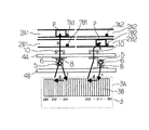
以下図1に基づき、プリント基板上に電子部品を装着する電子部品装着装置について、本発明の実施の形態を説明する。電子部品装着装置1には、各プリント基板を搬送すると共に各プリント基板を各位置決め装置で位置決めするように並設された二列の搬送装置2A、2Bと、電子部品を供給する部品供給装置3と、駆動源により一方向に移動可能(Y方向に往復移動可能)な一対のビーム4A、4Bと、それぞれ吸着ノズル5を備えて前記各ビーム4A、4Bに沿った方向に各駆動源により移動可能な装着ヘッド6とが設けられている。
An embodiment of the present invention will be described below with respect to an electronic component mounting apparatus that mounts electronic components on a printed circuit board with reference to FIG. The electronic
前記搬送装置2A、2Bは電子部品装着装置1の奥と手前の前後中間部に配設され、ベルトコンベアから構成される左搬送装置2A1、2B1と右搬送装置2A2、2B2とを備えると共に夫々位置決め固定する位置決め装置(図示せず)を備えている。左搬送装置2A1、2B1及び右搬送装置2A2、2B2には、それぞれ下流寄りに出没可能なストッパ7A1、7B1及び7A2、7B2が設けられる。
The
前記部品供給装置3は前記搬送装置2A、2Bの一外方、例えば搬送装置2A、2Bの手前側に配設され、電子部品装着装置1の装置本体に取り付けられるフィーダベース3Aと、このフィーダベース3A上に複数並設され種々の電子部品を夫々その部品取出し部(部品吸着位置)に1個ずつ供給する部品供給ユニット3B群とから構成される。
The
そして、X方向に長い前後一対の前記ビーム4A、4Bは、各Y方向リニアモータ9の駆動により左右一対の前後に延びたガイドに沿って前記各ビームに固定されたスライダが摺動して個別にY方向に移動する。前記Y方向リニアモータ9は、左右一対の基体1A、1Bに沿って固定された上下一対の固定子と、前記ビーム4A、4Bの両端部に設けられた取付板の下部に固定された可動子9Aとから構成される。
The pair of front and
また、前記ビーム4A、4Bにはその長手方向(X方向)にX方向リニアモータ19によりガイドに沿って移動する前記装着ヘッド6が夫々内側に設けられており、前記X方向リニアモータ19は各ビーム4A、4Bに固定された前後一対の固定子と、各固定子の間に位置して前記装着ヘッド6に設けられた可動子とから構成される。
The
従って、各装着ヘッド6は向き合うように各ビーム4A、4Bの内側に設けられ、同じ高さ位置で移動可能であり、前記搬送装置2A、2B上の対応するプリント基板Pや部品供給ユニット3Bの部品取出し位置上方を移動する。即ち、ビーム4A、4Bに設けられた両装着ヘッド6は、原則として部品供給ユニット3B群から同時に(同期ではない。)、電子部品の取出し作業を行い、ビーム4Aに設けられた装着ヘッド6は奥側の搬送装置2A上のプリント基板Pのみに装着し、ビーム4Bに設けられた装着ヘッド6は手前側の搬送装置2B上のプリント基板Pのみに装着するように、分担している。
Accordingly, each
そして、各装着ヘッド6には12本の各バネにより下方へ付勢されている吸着ノズル5が円周上に所定間隔を存して配設されており、各装着ヘッド6の3時と9時の位置に位置する吸着ノズル5により並設された複数の部品供給ユニット3Bから電子部品を同時に取出しすることも可能である。この吸着ノズル5は上下軸モータ20により昇降可能であり、またθ軸モータ21により装着ヘッド6を鉛直軸周りに回転させることにより、結果として各装着ヘッド6の各吸着ノズル5はX方向及びY方向に移動可能であり、垂直線回りに回転可能で、且つ上下動可能となっている。
Each
また、各装着ヘッド6には基板認識カメラ8が設けられ、位置決めされているプリント基板Pに付された位置決めマークを撮像する。各部品認識カメラ10は、各装着ヘッド6に設けられた各吸着ノズル5に吸着保持された電子部品を一括して撮像する。
In addition, each
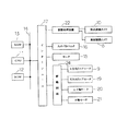
図3は電子部品装着装置1の電子部品装着に係る制御のための制御ブロックであり、以下説明する。電子部品装着装置1の各要素はCPU(セントラル・プロセッシング・ユニット)11が統括制御しており、この制御に係るプログラムを格納するROM(リ−ド・オンリー・メモリ)12及び各種データを格納するRAM(ランダム・アクセス・メモリ)13がバスライン14を介して接続されている。また、CPU11には操作画面等を表示するモニタ15及び該モニタ15の表示画面に形成された入力手段としてのタッチパネルスイッチ16がインターフェース17を介して接続されている。また、前記Y方向リニアモータ9等が駆動回路24、インターフェース17を介して前記CPU11に接続されている。
FIG. 3 is a control block for control related to electronic component mounting of the electronic
前記RAM13には、図4に示すように、部品装着に係るプリント基板Pの種類毎に装着データが記憶されており、その装着順序毎(ステップ番号毎)に、夫々のプリント基板Pの右側下部のコーナーを原点としたプリント基板P内での各電子部品の装着座標のX方向(図2(C)では上方向がプラス)、Y方向(図2(C)では左方向がプラス)及び装着角度情報や吸着ノズルの番号情報(「1」〜「12」で表示)、各部品供給ユニットの配置番号情報(FDR)、装着ヘッド6の番号情報(奥側のビーム4Aに設けられた装着ヘッドは「1」、手前側のビーム4Bに設けられた装着ヘッドは「2」で表示)、左右のプリント基板のうちの左(「L」で表示)か右(「R」で表示)かの基板位置情報、二列の搬送装置2A、2Bのうち奥側の搬送装置2Aは「B」と表示し、手前側の搬送装置2Bは「A」と表示する搬送レーン情報等が格納されている。
As shown in FIG. 4, the
この装着データによれば、ステップ番号「0001」〜「0012」及び「0025」〜「0036」は、手前側のビーム4Bに設けられた装着ヘッド6(ヘッド番号「2」)を使用して、手前側の搬送装置2Bの右搬送装置2B2上のプリント基板Pに電子部品を装着することを意味し、またステップ番号「0013」〜「0024」及び「0037」〜「0048」は、奥側のビーム4Aに設けられた装着ヘッド6(ヘッド番号「1」)を使用して、奥側の搬送装置2Aの左搬送装置2A1のプリント基板Pに電子部品を装着することを意味する。
According to this mounting data, the step numbers “0001” to “0012” and “0025” to “0036” use the mounting head 6 (head number “2”) provided on the
また、前記RAM13には、図5に示すように、前記各部品供給ユニットの部品供給ユニット配置番号に対応した各電子部品の種類(部品ID)の情報、即ち部品配置データが格納されており、更には形状データ・認識データ・制御データ・部品供給データから成る部品ライブラリデータ等が格納されている。
Further, as shown in FIG. 5, the
22はインターフェース17を介して前記CPU11に接続される認識処理装置で、前記基板認識カメラ8や部品認識カメラ10により撮像して取込まれた画像の認識処理が該認識処理装置22にて行われ、CPU11に処理結果が送出される。即ち、CPU11は基板認識カメラ8や部品認識カメラ10により撮像された画像を認識処理(位置ずれ量の算出など)するように指示を認識処理装置22に出力すると共に、認識処理結果を認識処理装置22から受取るものである。
A
以上の構成により、以下動作について説明する。先ず、図2(A)に示すように、初めにベルトコンベアから構成される奥側と手前側の搬送装置2A、2Bの左搬送装置2A1、2B1及び右搬送装置2A2、2B2は全て停止状態であって、ストッパ7A1、7B1及び7A2、7B2が上昇して搬送路内に突出してプリント基板Pを係止可能な状態にある。
With the above configuration, the operation will be described below. First, as shown in FIG. 2 (A), the left conveying devices 2A1 and 2B1 and the right conveying devices 2A2 and 2B2 of the conveying
次に、図2(B)に示すように、奥側の搬送装置2Aはストッパ7A1、7A2を上昇させたまま、上流側装置からプリント基板Pを受け継ぐために、左搬送装置2A1を運転状態とし、また手前側の搬送装置2Bはストッパ7B1を下降させ(ストッパ7A2は上昇したまま)、上流側装置からプリント基板Pを受け継ぐために、左搬送装置2A1、2B1及び右搬送装置2B2を運転状態とする。
Next, as shown in FIG. 2 (B), the
この状態で、図2(C)に示すように、奥側の搬送装置2Aでは上流側装置から移載されたプリント基板Pがストッパ7A1に係止し、手前側の搬送装置2Bでは上流側装置から移載されたプリント基板Pがストッパ7B2に係止するが、このプリント基板Pがストッパ7B1を通過したら、ストッパ7B1を上昇させる。
In this state, as shown in FIG. 2C, the printed circuit board P transferred from the upstream device is locked to the stopper 7A1 in the
そして、この奥側の搬送装置2Aではプリント基板Pを左搬送装置2A1の位置決め装置により、また手前側の搬送装置2Bではプリント基板Pを右搬送装置2B2の位置決め装置により、平面方向及び上下方向における位置決めがなされ、以下電子部品の装着動作に移ることとなる。なお、奥側の搬送装置2Aではプリント基板Pを右搬送装置2A2の位置決め装置により、また手前側の搬送装置2Bではプリント基板Pを左搬送装置2B2の位置決め装置により位置決めして、電子部品の装着動作を行ってもよく、いずれにおいても、各位置決め装置によりプリント基板を位置決めする位置が互いに搬送方向においてずらしているので、両装着ヘッド6が衝突することを防止することができる。
Then, in the
そして、各プリント基板Pの位置決めがされると、CPU11はRAM13に格納された装着データ(図4参照)に従って、両ビーム4A、4Bの装着ヘッド6が部品供給ユニット3B群から電子部品を同時(「同期」ではない。)に取出して、各プリント基板P上に同時に装着するように制御する。この電子部品の取出し及び装着に際して、Y方向については両ビーム4A、4Bが必要以上に近づかないように制御されると共にX方向については両装着ヘッド6が必要以上に近づかないように制御されて、両ビーム4A、4Bの装着ヘッド6の衝突が防止される。
When each printed circuit board P is positioned, the
初めに、ステップ番号「0001」から「0012」まで、部品供給ユニット3B群から手前側のビーム4Bに設けられた装着ヘッド6(ヘッド番号「2」)により電子部品が順に取出されると同時に、ステップ番号「0013」から「0024」まで、部品供給ユニット3B群から奥側のビーム4Bに設けられた装着ヘッド6(ヘッド番号「1」)により電子部品が順に取出される。即ち、ステップ番号「0001」において、手前側のビーム4Bに設けられた装着ヘッド6の吸着ノズル5のノズル番号「1」が配置番号「211」の部品供給ユニット3Bから電子部品を取出すと同時に、ステップ番号「0013」において、奥側のビーム4Aに設けられた装着ヘッド6の吸着ノズル5のノズル番号「1」が配置番号「241」の部品供給ユニット3Bから電子部品を取出すというように、それぞれ対応するステップ番号に従って12個の電子部品を吸着して取出す。
First, from step numbers “0001” to “0012”, electronic components are sequentially taken out by the mounting head 6 (head number “2”) provided on the
また、この取出した後は、両装着ヘッド6の吸着ノズル5を上昇させて、両ビーム4A、4Bの装着ヘッド6を各部品認識カメラ10上方を通過させ、この移動中に両装着ヘッド6の12本の吸着ノズル5に吸着保持された12個の電子部品を一括して撮像して、この撮像された画像を認識処理装置22が認識処理して吸着ノズル5に対する位置ズレを把握する。
Further, after the removal, the
その後、両ビーム4A、4Bの装着ヘッド6に設けられた基板認識カメラ8を各プリント基板P上方へ移動させて、奥側の搬送装置2Aの左搬送装置2A1、手前側の搬送装置2Bの右搬送装置2B2上で位置決めされている各プリント基板Pに付された位置決めマークを撮像し、この撮像された画像を認識処理装置22が認識処理して各プリント基板Pの位置を把握する。そして、装着データの装着座標にそれぞれのプリント基板Pの位置認識結果及び各部品認識処理結果を加味して、各吸着ノズル5が位置ずれを補正しつつ、それぞれ電子部品を各プリント基板P上に装着する。
After that, the
即ち、ステップ番号「0001」から「0012」までの電子部品について、手前側のビーム4Bに設けられた装着ヘッド6に設けられ右側に位置した吸着ノズル5に吸着保持された電子部品を手前側の搬送装置2Bの右搬送装置2B2上のプリント基板P上に補正しつつ順次装着すると同時に、ステップ番号「0013」から「0024」までの電子部品について、奥側のビーム4Aに設けられ左側に位置した装着ヘッド6に設けられた吸着ノズル5に吸着保持された電子部品を奥側の搬送装置2Aの左搬送装置2A1上のプリント基板P上に補正しつつ順次装着する。この場合にも、両ビーム4A、4Bの装着ヘッド6が衝突しないように対応するY方向リニアモータ9及びX方向リニアモータ19がCPU11により制御される。
That is, for the electronic components from step numbers “0001” to “0012”, the electronic components sucked and held by the
次に、ステップ番号「0025」から「0036」まで、部品供給ユニット3B群から手前側のビーム4Bに設けられた装着ヘッド6により電子部品が順に取出されると同時に、ステップ番号「0037」から「0048」まで、部品供給ユニット3B群から奥側のビーム4Aに設けられた装着ヘッド6により電子部品が順に取出される。
Next, from step numbers “0025” to “0036”, electronic components are sequentially taken out from the
この場合、ステップ番号「0001」から「0012」までは、手前側のビーム4Bの装着ヘッド6は部品供給ユニット配置番号「211」から「222」までの部品供給ユニット3B群から電子部品を取出し、またステップ番号「0013」から「0024」までは、奥側のビーム4Aの装着ヘッド6は部品供給ユニット配置番号「241」から「252」までの部品供給ユニット3B群から電子部品を取出すので、図6に示すように、手前側のビーム4Bの装着ヘッド6が部品供給ユニット3B群の右半分の領域から取出すと共に奥側のビーム4Aの装着ヘッド6は左半分の領域から取出していたが、ステップ番号「0025」から「0036」まで及びステップ番号「0037」から「0048」までは、図7に示すように、両装着ヘッド6を左右入れ替える必要がある。
In this case, from the step numbers “0001” to “0012”, the mounting
即ち、図7に示すように、部品供給ユニット3B群からの電子部品の取出しに際して、今まで左方に位置していた奥側のビーム4Aの装着ヘッド6は右方に、また今まで右方に位置していた手前側のビーム4Bの装着ヘッド6は右方に移動しなければならず、電子部品の取出し後の各プリント基板Pへの装着に際しては再び元に戻し、奥側のビーム4Aの装着ヘッド6を左方に且つ手前側のビーム4Bの装着ヘッド6を左方に移動させることとなる。
That is, as shown in FIG. 7, when the electronic component is taken out from the
また、ステップ番号「0025」から「0036」、「0037」から「0048」までの電子部品を取出した後は、両装着ヘッド6の吸着ノズル5を上昇させて、両ビーム4A、4Bの装着ヘッド6を部品認識カメラ10上方を通過させ、この移動中に両装着ヘッド6の12本の吸着ノズル5に吸着保持された12個の電子部品を一括して撮像して、この撮像された画像を認識処理装置22が認識処理して吸着ノズル5に対する位置ズレを把握する。
In addition, after taking out the electronic components from step numbers “0025” to “0036” and “0037” to “0048”, the
そして、装着データの装着座標にそれぞれのプリント基板Pの位置認識結果及び各部品認識処理結果を加味して、各吸着ノズル5が位置ずれを補正しつつ、それぞれ電子部品を各プリント基板P上に装着する。即ち、ステップ番号「0025」から「0036」までの電子部品について、手前側のビーム4Bに設けられた装着ヘッド6に設けられた吸着ノズル5に吸着保持された電子部品を手前側の搬送装置2Bの右搬送装置2B2上のプリント基板P上に補正しつつ順次装着すると同時に、ステップ番号「0037」から「0048」までの電子部品について、奥側のビーム4Aに設けられた装着ヘッド6に設けられた吸着ノズル5に吸着保持された電子部品を奥側の搬送装置2Aの左搬送装置2A1上のプリント基板P上に補正しつつ順次装着する。
Then, by adding the position recognition result of each printed circuit board P and the result of each component recognition process to the mounting coordinates of the mounting data, each
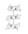
次に、各プリント基板P上への全ての電子部品の装着を終了した後に、下流側装置へこれらのプリント基板Pを排出する動作について、図8に基づいて説明する。先ず、図8(A)に示すように、奥側の搬送装置2Aの左搬送装置2A1上のプリント基板Pはストッパ7A1に係止し、また手前側の搬送装置2Bの右搬送装置2B2上のプリント基板Pはストッパ7B2に係止して位置決め状態にある状態で、全ての電子部品の装着動作が終了する。次に、図8(B)に示すように、奥側の搬送装置2Aにおいては、ストッパ7A1を下降させて、左搬送装置2A1及び右搬送装置2A2を運転させて、プリント基板Pを左搬送装置2A1から右搬送装置2A2への移載を開始させ、手前側の搬送装置2Bでは、右搬送装置2B2のストッパ7B2に装着済みのプリント基板Pが係止すると共に上流側装置からの新たなプリント基板Pの受け継ぎを開始する。
Next, the operation of discharging these printed circuit boards P to the downstream apparatus after all electronic components have been mounted on each printed circuit board P will be described with reference to FIG. First, as shown in FIG. 8A, the printed circuit board P on the left transport device 2A1 of the
そして、図8(C)に示すように、奥側の搬送装置2Aでは、左搬送装置2A1上のプリント基板Pがストッパ7A1を通過したら、このストッパ7A1が上昇して新たなプリント基板Pの受け継ぎが開始される。次に、図8(D)に示すように、奥側の搬送装置2Aでは、受け継いだ新たなプリント基板Pがストッパ7A1に係止すると共に装着済みのプリント基板はストッパ7A2に係止したら、左搬送装置2A1及び右搬送装置2A2を停止させ、手前側の搬送装置2Bでは、受け継いだ新たなプリント基板Pがストッパ7B1に係止したら、左搬送装置2B1を停止させる。
As shown in FIG. 8C, in the
次に、図8(E)に示すように、奥側の搬送装置2Aの右搬送装置2A2及び手前側の搬送装置2Bの右搬送装置2B2のストッパ7A2、7B2を下降させると共に両右搬送装置2A2及び2B2の運転を開始させ、下流側装置に装着済みの各プリント基板Pを受け渡す。
Next, as shown in FIG. 8E, the stoppers 7A2 and 7B2 of the right transport device 2A2 of the
そして、図8(F)に示すように、下流側装置への装着済みの各プリント基板Pの排出が完了したら、両ストッパ7A2、7B2を上昇させる共に両右搬送装置2A2及び2B2を停止させる。次いで、図8(G)に示すように、手前側の搬送装置2Bの左搬送装置2B1のストッパ7B1を下降させると共に左右搬送装置2B1及び2B2の運転を開始させ、新たなプリント基板Pを左搬送装置2B1から右搬送装置2B2へと移載する。
Then, as shown in FIG. 8 (F), when the discharge of each printed circuit board P attached to the downstream apparatus is completed, both stoppers 7A2 and 7B2 are raised and both right transport apparatuses 2A2 and 2B2 are stopped. Next, as shown in FIG. 8G, the stopper 7B1 of the left transport device 2B1 of the
そして、図8(H)に示すように、手前側の搬送装置2Bの右搬送装置2B2のストッパ7B2に新たなプリント基板Pが係止するので、手前側の搬送装置2Bの右搬送装置2B2及び奥側の搬送装置2Aの左搬送装置2A1において、各新たなプリント基板Pが各ストッパ7B2、7A1に係止し、装着済みのプリント基板Pの下流側装置への受け渡し及び新たなプリント基板Pの上流側装置からの受け継ぎが終了する。以後は、前述したように、これらのプリント基板Pを位置決めして、電子部品の装着動作に移ることができる。
Then, as shown in FIG. 8H, the new printed circuit board P is locked to the stopper 7B2 of the right transport device 2B2 of the
以上のように、本実施形態によれば、設置スペースの関係等から部品供給装置3を搬送装置2A、2Bの一外方に配設し、両ビーム4A、4Bに設けられた装着ヘッド6が部品供給装置3に同時に乗り入れて、同時進行する形で電子部品の吸着取出しを行い、各プリント基板Pへの装着動作も同時に行うので、プリント基板の生産効率の向上を図ることができる。特に、プリント基板への装着点数が多いプリント基板の生産に効果的である。また、搬送装置が二列なので、プリント基板への装着終了後、すぐに下流側へ排出することができる。更に、両搬送装置に夫々搬送させるプリント基板は、同一種類でも、異なる種類のものでもよい。
As described above, according to the present embodiment, the
装着データと一対になった基板種毎に設けられたデータであって、搬送モード(例えば、一列の搬送装置又は二列の搬送装置のモード)を指定するデータによって、上述した基板の搬送及びタイミングで行わせるように制御することができる。 The above-described substrate transport and timing according to data that is provided for each substrate type paired with the mounting data and that designates a transport mode (for example, a mode of a single-row transport device or a double-row transport device). It can be controlled to be performed in.
なお、電子部品の品種が少なければ、フィーダベース上の片側寄りに配設された部品供給ユニットから電子部品を取出し、各ビームに設けられた装着ヘッドを左右入れ替えないようにしてもよい。 If there are few types of electronic components, the electronic components may be taken out from a component supply unit disposed on one side of the feeder base so that the mounting heads provided on each beam are not switched left and right.
また、大きなプリント基板にあっては、両搬送装置ともに左右の搬送装置にまたがって位置決めして電子部品を装着してもよいし、どちらかの搬送装置のみを使用して左右の搬送装置にまたがって位置決めして電子部品を装着してもよい。 For a large printed circuit board, both transport devices may be positioned across the left and right transport devices and electronic components may be mounted, or only one of the transport devices may be used to span the left and right transport devices. The electronic parts may be mounted after positioning.
以上のように本発明の実施態様について説明したが、上述の説明に基づいて当業者にとって種々の代替例、修正又は変形が可能であり、本発明はその趣旨を逸脱しない範囲で前述の種々の代替例、修正又は変形を包含するものである。 Although the embodiments of the present invention have been described above, various alternatives, modifications, and variations can be made by those skilled in the art based on the above description, and the present invention is not limited to the various embodiments described above without departing from the spirit of the present invention. It encompasses alternatives, modifications or variations.
1 電子部品装着装置
2A、2B 搬送装置
3 部品供給装置
3A フィーダベース
3B 部品供給ユニット
4A、4B ビーム
5 吸着ノズル
6 装着ヘッド
11 CPU
13 RAM
DESCRIPTION OF
13 RAM
Claims (2)
Priority Applications (1)
| Application Number | Priority Date | Filing Date | Title |
|---|---|---|---|
| JP2008243471A JP5118595B2 (en) | 2008-09-23 | 2008-09-23 | Mounting method of electronic parts |
Applications Claiming Priority (1)
| Application Number | Priority Date | Filing Date | Title |
|---|---|---|---|
| JP2008243471A JP5118595B2 (en) | 2008-09-23 | 2008-09-23 | Mounting method of electronic parts |
Publications (2)
| Publication Number | Publication Date |
|---|---|
| JP2010080461A true JP2010080461A (en) | 2010-04-08 |
| JP5118595B2 JP5118595B2 (en) | 2013-01-16 |
Family
ID=42210614
Family Applications (1)
| Application Number | Title | Priority Date | Filing Date |
|---|---|---|---|
| JP2008243471A Active JP5118595B2 (en) | 2008-09-23 | 2008-09-23 | Mounting method of electronic parts |
Country Status (1)
| Country | Link |
|---|---|
| JP (1) | JP5118595B2 (en) |
Cited By (2)
| Publication number | Priority date | Publication date | Assignee | Title |
|---|---|---|---|---|
| JP2015082579A (en) * | 2013-10-23 | 2015-04-27 | パナソニックIpマネジメント株式会社 | Component mounting system |
| WO2019043903A1 (en) * | 2017-09-01 | 2019-03-07 | ヤマハ発動機株式会社 | Component mounting method and component mounting apparatus |
Citations (6)
| Publication number | Priority date | Publication date | Assignee | Title |
|---|---|---|---|---|
| JP2002076692A (en) * | 2000-08-30 | 2002-03-15 | Sanyo Electric Co Ltd | Electronic component mounting apparatus |
| JP2002204099A (en) * | 2000-12-27 | 2002-07-19 | Sanyo Electric Co Ltd | Electronic component mounting machine |
| JP2002353692A (en) * | 2001-05-22 | 2002-12-06 | Sanyo Electric Co Ltd | Electronic component mounter |
| JP2002359493A (en) * | 2001-05-30 | 2002-12-13 | Sanyo Electric Co Ltd | Electronic component mounting device |
| JP2004128400A (en) * | 2002-10-07 | 2004-04-22 | Fuji Mach Mfg Co Ltd | Component mounting apparatus, program for controlling operation of the same apparatus, and component mounting system |
| JP2006270050A (en) * | 2005-02-25 | 2006-10-05 | Matsushita Electric Ind Co Ltd | Device mounter and substrate positioning method |
-
2008
- 2008-09-23 JP JP2008243471A patent/JP5118595B2/en active Active
Patent Citations (6)
| Publication number | Priority date | Publication date | Assignee | Title |
|---|---|---|---|---|
| JP2002076692A (en) * | 2000-08-30 | 2002-03-15 | Sanyo Electric Co Ltd | Electronic component mounting apparatus |
| JP2002204099A (en) * | 2000-12-27 | 2002-07-19 | Sanyo Electric Co Ltd | Electronic component mounting machine |
| JP2002353692A (en) * | 2001-05-22 | 2002-12-06 | Sanyo Electric Co Ltd | Electronic component mounter |
| JP2002359493A (en) * | 2001-05-30 | 2002-12-13 | Sanyo Electric Co Ltd | Electronic component mounting device |
| JP2004128400A (en) * | 2002-10-07 | 2004-04-22 | Fuji Mach Mfg Co Ltd | Component mounting apparatus, program for controlling operation of the same apparatus, and component mounting system |
| JP2006270050A (en) * | 2005-02-25 | 2006-10-05 | Matsushita Electric Ind Co Ltd | Device mounter and substrate positioning method |
Cited By (4)
| Publication number | Priority date | Publication date | Assignee | Title |
|---|---|---|---|---|
| JP2015082579A (en) * | 2013-10-23 | 2015-04-27 | パナソニックIpマネジメント株式会社 | Component mounting system |
| WO2019043903A1 (en) * | 2017-09-01 | 2019-03-07 | ヤマハ発動機株式会社 | Component mounting method and component mounting apparatus |
| JPWO2019043903A1 (en) * | 2017-09-01 | 2020-02-27 | ヤマハ発動機株式会社 | Component mounting method and component mounting device |
| JP7017574B2 (en) | 2017-09-01 | 2022-02-08 | ヤマハ発動機株式会社 | Component mounting method and component mounting device |
Also Published As
| Publication number | Publication date |
|---|---|
| JP5118595B2 (en) | 2013-01-16 |
Similar Documents
| Publication | Publication Date | Title |
|---|---|---|
| JP4846649B2 (en) | Electronic component mounting device | |
| JP4942497B2 (en) | Electronic component mounting device | |
| JP5281546B2 (en) | Electronic component mounting method, electronic component mounting device, electronic component mounting order determination method for electronic component mounting device, and mounting data creation method for electronic component mounting device | |
| JP4744407B2 (en) | Electronic component mounting device | |
| JP5118595B2 (en) | Mounting method of electronic parts | |
| JP4792346B2 (en) | Electronic component mounting apparatus and electronic component mounting method | |
| JP2008159855A (en) | Apparatus for mounting electronic component | |
| JP5085509B2 (en) | Electronic component mounting method, electronic component mounting apparatus, and electronic component mounting order determination method for electronic component mounting apparatus | |
| JP6572437B2 (en) | Component mounting apparatus and component mounting method | |
| JP2011035081A (en) | Method for mounting electronic component and device for mounting electronic component | |
| JP2012094925A (en) | Method for mounting electronic component | |
| JP5027039B2 (en) | Mounting method of electronic parts | |
| JP2017011024A (en) | Electronic component mounting system | |
| JP4933507B2 (en) | Mounting method of electronic parts | |
| JP5321474B2 (en) | Component mounting apparatus and component mounting method | |
| JP5075096B2 (en) | Electronic component mounting device | |
| JP4933508B2 (en) | Mounting method of electronic parts | |
| JP5370204B2 (en) | Component mounting apparatus and component mounting method | |
| JP5755505B2 (en) | Electronic component mounting method and mounting device | |
| JP2011134812A (en) | Mounting method of electronic component and mounting device thereof | |
| JP5234013B2 (en) | Component mounting apparatus and component mounting method | |
| JP2008135608A (en) | Electronic-component mounting device | |
| US20200022292A1 (en) | Movement error detection apparatus of mounting head, and component mounting apparatus | |
| JP5096385B2 (en) | Electronic component mounting device | |
| JP2012119511A (en) | Electronic component mounting device, electronic component mounting system, and electronic component mounting method |
Legal Events
| Date | Code | Title | Description |
|---|---|---|---|
| A621 | Written request for application examination |
Free format text: JAPANESE INTERMEDIATE CODE: A621 Effective date: 20101029 |
|
| A977 | Report on retrieval |
Free format text: JAPANESE INTERMEDIATE CODE: A971007 Effective date: 20120229 |
|
| A131 | Notification of reasons for refusal |
Free format text: JAPANESE INTERMEDIATE CODE: A131 Effective date: 20120306 |
|
| A521 | Request for written amendment filed |
Free format text: JAPANESE INTERMEDIATE CODE: A523 Effective date: 20120507 |
|
| TRDD | Decision of grant or rejection written | ||
| A01 | Written decision to grant a patent or to grant a registration (utility model) |
Free format text: JAPANESE INTERMEDIATE CODE: A01 Effective date: 20120920 |
|
| A01 | Written decision to grant a patent or to grant a registration (utility model) |
Free format text: JAPANESE INTERMEDIATE CODE: A01 |
|
| A61 | First payment of annual fees (during grant procedure) |
Free format text: JAPANESE INTERMEDIATE CODE: A61 Effective date: 20121019 |
|
| R150 | Certificate of patent or registration of utility model |
Free format text: JAPANESE INTERMEDIATE CODE: R150 Ref document number: 5118595 Country of ref document: JP Free format text: JAPANESE INTERMEDIATE CODE: R150 |
|
| FPAY | Renewal fee payment (event date is renewal date of database) |
Free format text: PAYMENT UNTIL: 20151026 Year of fee payment: 3 |
|
| S111 | Request for change of ownership or part of ownership |
Free format text: JAPANESE INTERMEDIATE CODE: R313113 |
|
| R350 | Written notification of registration of transfer |
Free format text: JAPANESE INTERMEDIATE CODE: R350 |
|
| R250 | Receipt of annual fees |
Free format text: JAPANESE INTERMEDIATE CODE: R250 |
|
| R250 | Receipt of annual fees |
Free format text: JAPANESE INTERMEDIATE CODE: R250 |
|
| R250 | Receipt of annual fees |
Free format text: JAPANESE INTERMEDIATE CODE: R250 |
|
| R250 | Receipt of annual fees |
Free format text: JAPANESE INTERMEDIATE CODE: R250 |
|
| R250 | Receipt of annual fees |
Free format text: JAPANESE INTERMEDIATE CODE: R250 |
|
| R250 | Receipt of annual fees |
Free format text: JAPANESE INTERMEDIATE CODE: R250 |
|
| R250 | Receipt of annual fees |
Free format text: JAPANESE INTERMEDIATE CODE: R250 |
|
| R250 | Receipt of annual fees |
Free format text: JAPANESE INTERMEDIATE CODE: R250 |
|
| R250 | Receipt of annual fees |
Free format text: JAPANESE INTERMEDIATE CODE: R250 |