JP2010073962A - 半導体発光素子 - Google Patents
半導体発光素子 Download PDFInfo
- Publication number
- JP2010073962A JP2010073962A JP2008240893A JP2008240893A JP2010073962A JP 2010073962 A JP2010073962 A JP 2010073962A JP 2008240893 A JP2008240893 A JP 2008240893A JP 2008240893 A JP2008240893 A JP 2008240893A JP 2010073962 A JP2010073962 A JP 2010073962A
- Authority
- JP
- Japan
- Prior art keywords
- crystal
- nano
- layer
- gan
- axis
- Prior art date
- Legal status (The legal status is an assumption and is not a legal conclusion. Google has not performed a legal analysis and makes no representation as to the accuracy of the status listed.)
- Granted
Links
Images


Landscapes
- Led Devices (AREA)
Abstract
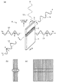
【解決手段】基板上に、n型GaN層1、InGaN活性層2、p型GaN層3を有するウルツ構造の半導体結晶4がc軸成長されて成る半導体発光素子において、前記の各層1,2,3による半導体結晶4を、基板からナノサイズのシート状に立設する。したがって、大きなアスペクト比の差で成長させることで、図1(b)で示すように、InGaN活性層2が、両側の層1,層3よりも格子定数が大きいために、短手(厚み)方向では外部に膨出して応力が緩和されているのに対して、図1(c)で示すように、長手(幅)方向では変形しておらず、応力緩和が許容されない。これによって、応力無印加時には縮退している2つの価電子帯HHとLHとが互いに分離し、HH帯へのキャリア遷移によるc軸と垂直方向に伝播する直線偏光した光11〜14を支配的に発光させることができる。
【選択図】図1
Description
2 GaN/InGaN量子井戸層(活性層)
3 p型GaN層
4 ナノサイズの薄いシート(壁)状GaN結晶
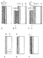
21 半導体発光素子
22 c面サファイア基板
23 n型GaN層
24 Cr薄膜層
25 p型プレーナGaN層
26 n型電極
27 p型電極
28 透明導電膜
29 反射層
Claims (8)
- 基板上に、少なくともp型層、活性層、n型層を有するウルツ構造の半導体結晶がc軸成長されて成る半導体発光素子において、
前記の各層による半導体結晶が、基板からナノサイズのシート状に立設されることを特徴とする半導体発光素子。 - 前記ナノサイズのシート状結晶の長手方向の軸が、m軸またはa軸に平行であることを特徴とする請求項1記載の半導体発光素子。
- 前記ナノサイズのシート状結晶は、前記p型層、活性層、n型層が、GaN、InGaN、GaNまたはAlGaN、GaN、AlGaNから、それぞれ成ることを特徴とする請求項1または2記載の半導体発光素子。
- 前記ナノサイズのシート状結晶は、1nm以上、30nm以下の厚さに形成されることを特徴とする請求項1〜3のいずれか1項に記載の半導体発光素子。
- 前記ナノサイズのシート状結晶は、前記基板上に、複数のアレイ状に形成されていることを特徴とする請求項1〜4のいずれか1項に記載の半導体発光素子。
- 前記ナノサイズのシート状結晶は、2次元フォトニック結晶配列となっていることを特徴とする請求項5記載の半導体発光素子。
- アレイ状に形成された各ナノサイズのシート状結晶において、p型層が、該結晶の成長に伴い、相互に隣接する結晶間が結合されていることを特徴とする請求項5または6記載の半導体発光素子。
- 前記p型層とp型電極との間に透明導電膜を備え、この透明導電膜は活性層から発光された波長の光に対して、70%以上の透過率および1kohm/square以下のシート抵抗を有することを特徴とする請求項1〜7のいずれか1項に記載の半導体発光素子。
Priority Applications (1)
| Application Number | Priority Date | Filing Date | Title |
|---|---|---|---|
| JP2008240893A JP5341446B2 (ja) | 2008-09-19 | 2008-09-19 | 半導体発光素子 |
Applications Claiming Priority (1)
| Application Number | Priority Date | Filing Date | Title |
|---|---|---|---|
| JP2008240893A JP5341446B2 (ja) | 2008-09-19 | 2008-09-19 | 半導体発光素子 |
Publications (2)
| Publication Number | Publication Date |
|---|---|
| JP2010073962A true JP2010073962A (ja) | 2010-04-02 |
| JP5341446B2 JP5341446B2 (ja) | 2013-11-13 |
Family
ID=42205468
Family Applications (1)
| Application Number | Title | Priority Date | Filing Date |
|---|---|---|---|
| JP2008240893A Expired - Fee Related JP5341446B2 (ja) | 2008-09-19 | 2008-09-19 | 半導体発光素子 |
Country Status (1)
| Country | Link |
|---|---|
| JP (1) | JP5341446B2 (ja) |
Cited By (2)
| Publication number | Priority date | Publication date | Assignee | Title |
|---|---|---|---|---|
| WO2012020559A1 (ja) * | 2010-08-09 | 2012-02-16 | パナソニック株式会社 | 半導体発光デバイス |
| KR102396825B1 (ko) * | 2020-11-06 | 2022-05-10 | 한양대학교 산학협력단 | 초저전력 소모 트랜지스터 |
Citations (1)
| Publication number | Priority date | Publication date | Assignee | Title |
|---|---|---|---|---|
| JP2008016836A (ja) * | 2006-07-03 | 2008-01-24 | Samsung Electro Mech Co Ltd | 偏光性を有する半導体発光素子 |
-
2008
- 2008-09-19 JP JP2008240893A patent/JP5341446B2/ja not_active Expired - Fee Related
Patent Citations (1)
| Publication number | Priority date | Publication date | Assignee | Title |
|---|---|---|---|---|
| JP2008016836A (ja) * | 2006-07-03 | 2008-01-24 | Samsung Electro Mech Co Ltd | 偏光性を有する半導体発光素子 |
Cited By (3)
| Publication number | Priority date | Publication date | Assignee | Title |
|---|---|---|---|---|
| WO2012020559A1 (ja) * | 2010-08-09 | 2012-02-16 | パナソニック株式会社 | 半導体発光デバイス |
| JP4981996B2 (ja) * | 2010-08-09 | 2012-07-25 | パナソニック株式会社 | 半導体発光デバイス |
| KR102396825B1 (ko) * | 2020-11-06 | 2022-05-10 | 한양대학교 산학협력단 | 초저전력 소모 트랜지스터 |
Also Published As
| Publication number | Publication date |
|---|---|
| JP5341446B2 (ja) | 2013-11-13 |
Similar Documents
| Publication | Publication Date | Title |
|---|---|---|
| JP5450776B2 (ja) | 超格子構造のウェル層及び/又は超格子構造のバリア層を有する発光ダイオード | |
| KR101342664B1 (ko) | 자외선 발광소자 | |
| JP4572270B2 (ja) | 窒化物半導体素子およびその製造方法 | |
| US8344409B2 (en) | Optoelectronic device and method for manufacturing the same | |
| CN102150287B (zh) | 发光器件 | |
| US20130140519A1 (en) | Light emitting diode | |
| KR101550117B1 (ko) | 광전 소자 및 그 제조 방법 | |
| JP4110222B2 (ja) | 発光ダイオード | |
| KR100658938B1 (ko) | 나노 로드를 갖는 발광 소자 및 그의 제조 방법 | |
| KR20110131801A (ko) | 발광 소자 및 다중 파장의 광을 만드는 방법 | |
| KR101644156B1 (ko) | 양자우물 구조의 활성 영역을 갖는 발광 소자 | |
| KR20120128398A (ko) | 마이크로 어레이 형태의 질화물 발광 소자 및 그 제조 방법 | |
| JP2009239075A (ja) | 発光素子 | |
| US8946736B2 (en) | Optoelectronic device and method for manufacturing the same | |
| US8759857B2 (en) | Light emitting diode | |
| CN103035797A (zh) | 完全禁带光子晶体结构、其制备方法及一种发光二极管 | |
| JP2015119108A (ja) | 紫外線発光素子 | |
| JP5341446B2 (ja) | 半導体発光素子 | |
| JP3157124U (ja) | 窒化ガリウム系発光ダイオードの構造 | |
| Hayashi et al. | Thermally engineered flip-chip InGaN/GaN well-ordered nanocolumn array LEDs | |
| WO2011163186A1 (en) | Engineering emission wavelengths in laser and light emitting devices | |
| RU2426197C1 (ru) | Нитридное полупроводниковое устройство | |
| JP2011082248A (ja) | 半導体発光素子及びその製造方法、並びにランプ | |
| KR100765722B1 (ko) | 나노 로드를 갖는 발광 소자 및 그의 제조 방법 | |
| JP2004165267A (ja) | 半導体発光素子および発光表示装置、ならびにそれらの製造方法 |
Legal Events
| Date | Code | Title | Description |
|---|---|---|---|
| A621 | Written request for application examination |
Free format text: JAPANESE INTERMEDIATE CODE: A621 Effective date: 20110421 |
|
| A711 | Notification of change in applicant |
Free format text: JAPANESE INTERMEDIATE CODE: A712 Effective date: 20120111 |
|
| A977 | Report on retrieval |
Free format text: JAPANESE INTERMEDIATE CODE: A971007 Effective date: 20120912 |
|
| A131 | Notification of reasons for refusal |
Free format text: JAPANESE INTERMEDIATE CODE: A131 Effective date: 20120925 |
|
| A521 | Written amendment |
Free format text: JAPANESE INTERMEDIATE CODE: A523 Effective date: 20121031 |
|
| TRDD | Decision of grant or rejection written | ||
| A01 | Written decision to grant a patent or to grant a registration (utility model) |
Free format text: JAPANESE INTERMEDIATE CODE: A01 Effective date: 20130730 |
|
| A61 | First payment of annual fees (during grant procedure) |
Free format text: JAPANESE INTERMEDIATE CODE: A61 Effective date: 20130808 |
|
| R150 | Certificate of patent or registration of utility model |
Free format text: JAPANESE INTERMEDIATE CODE: R150 |
|
| LAPS | Cancellation because of no payment of annual fees |