JP2010073725A - 電子部品及び電子部品の製造方法 - Google Patents
電子部品及び電子部品の製造方法 Download PDFInfo
- Publication number
- JP2010073725A JP2010073725A JP2008236221A JP2008236221A JP2010073725A JP 2010073725 A JP2010073725 A JP 2010073725A JP 2008236221 A JP2008236221 A JP 2008236221A JP 2008236221 A JP2008236221 A JP 2008236221A JP 2010073725 A JP2010073725 A JP 2010073725A
- Authority
- JP
- Japan
- Prior art keywords
- metal member
- opening
- electrode
- carbon nanotube
- film
- Prior art date
- Legal status (The legal status is an assumption and is not a legal conclusion. Google has not performed a legal analysis and makes no representation as to the accuracy of the status listed.)
- Granted
Links
- 238000004519 manufacturing process Methods 0.000 title claims abstract description 15
- 239000002184 metal Substances 0.000 claims abstract description 82
- 229910052751 metal Inorganic materials 0.000 claims abstract description 82
- OKTJSMMVPCPJKN-UHFFFAOYSA-N Carbon Chemical compound [C] OKTJSMMVPCPJKN-UHFFFAOYSA-N 0.000 claims abstract description 81
- 239000002041 carbon nanotube Substances 0.000 claims abstract description 80
- 229910021393 carbon nanotube Inorganic materials 0.000 claims abstract description 80
- 239000000758 substrate Substances 0.000 claims abstract description 21
- 239000011347 resin Substances 0.000 claims description 4
- 229920005989 resin Polymers 0.000 claims description 4
- 229920001187 thermosetting polymer Polymers 0.000 claims description 2
- 239000004065 semiconductor Substances 0.000 abstract description 45
- 238000006073 displacement reaction Methods 0.000 abstract 1
- 238000002844 melting Methods 0.000 description 45
- 230000008018 melting Effects 0.000 description 44
- 238000000034 method Methods 0.000 description 11
- 239000010953 base metal Substances 0.000 description 10
- 229910000679 solder Inorganic materials 0.000 description 7
- 239000004925 Acrylic resin Substances 0.000 description 4
- 239000010949 copper Substances 0.000 description 4
- 239000000565 sealant Substances 0.000 description 4
- 238000013459 approach Methods 0.000 description 3
- 239000007789 gas Substances 0.000 description 3
- 230000008569 process Effects 0.000 description 3
- 230000001681 protective effect Effects 0.000 description 3
- 229920000178 Acrylic resin Polymers 0.000 description 2
- XKRFYHLGVUSROY-UHFFFAOYSA-N Argon Chemical compound [Ar] XKRFYHLGVUSROY-UHFFFAOYSA-N 0.000 description 2
- 229910020830 Sn-Bi Inorganic materials 0.000 description 2
- 229910018728 Sn—Bi Inorganic materials 0.000 description 2
- 229910045601 alloy Inorganic materials 0.000 description 2
- 239000000956 alloy Substances 0.000 description 2
- 238000005229 chemical vapour deposition Methods 0.000 description 2
- 230000008602 contraction Effects 0.000 description 2
- 238000011161 development Methods 0.000 description 2
- 239000003822 epoxy resin Substances 0.000 description 2
- 230000001771 impaired effect Effects 0.000 description 2
- 239000002923 metal particle Substances 0.000 description 2
- 229920000647 polyepoxide Polymers 0.000 description 2
- 239000000843 powder Substances 0.000 description 2
- KCTAWXVAICEBSD-UHFFFAOYSA-N prop-2-enoyloxy prop-2-eneperoxoate Chemical compound C=CC(=O)OOOC(=O)C=C KCTAWXVAICEBSD-UHFFFAOYSA-N 0.000 description 2
- 238000004544 sputter deposition Methods 0.000 description 2
- RYGMFSIKBFXOCR-UHFFFAOYSA-N Copper Chemical compound [Cu] RYGMFSIKBFXOCR-UHFFFAOYSA-N 0.000 description 1
- UFHFLCQGNIYNRP-UHFFFAOYSA-N Hydrogen Chemical compound [H][H] UFHFLCQGNIYNRP-UHFFFAOYSA-N 0.000 description 1
- HSFWRNGVRCDJHI-UHFFFAOYSA-N alpha-acetylene Natural products C#C HSFWRNGVRCDJHI-UHFFFAOYSA-N 0.000 description 1
- CAVCGVPGBKGDTG-UHFFFAOYSA-N alumanylidynemethyl(alumanylidynemethylalumanylidenemethylidene)alumane Chemical compound [Al]#C[Al]=C=[Al]C#[Al] CAVCGVPGBKGDTG-UHFFFAOYSA-N 0.000 description 1
- 229910052782 aluminium Inorganic materials 0.000 description 1
- XAGFODPZIPBFFR-UHFFFAOYSA-N aluminium Chemical compound [Al] XAGFODPZIPBFFR-UHFFFAOYSA-N 0.000 description 1
- 229910052786 argon Inorganic materials 0.000 description 1
- 229910052799 carbon Inorganic materials 0.000 description 1
- 239000012159 carrier gas Substances 0.000 description 1
- 239000003054 catalyst Substances 0.000 description 1
- 229910052802 copper Inorganic materials 0.000 description 1
- 238000009713 electroplating Methods 0.000 description 1
- 238000005530 etching Methods 0.000 description 1
- 125000002534 ethynyl group Chemical group [H]C#C* 0.000 description 1
- 238000012986 modification Methods 0.000 description 1
- 230000004048 modification Effects 0.000 description 1
- 230000002093 peripheral effect Effects 0.000 description 1
- 238000007747 plating Methods 0.000 description 1
- 230000009467 reduction Effects 0.000 description 1
- 229910052710 silicon Inorganic materials 0.000 description 1
- 239000010703 silicon Substances 0.000 description 1
- 230000007480 spreading Effects 0.000 description 1
- 238000003892 spreading Methods 0.000 description 1
- 238000012360 testing method Methods 0.000 description 1
Images


Classifications
-
- H—ELECTRICITY
- H01—ELECTRIC ELEMENTS
- H01L—SEMICONDUCTOR DEVICES NOT COVERED BY CLASS H10
- H01L24/00—Arrangements for connecting or disconnecting semiconductor or solid-state bodies; Methods or apparatus related thereto
- H01L24/01—Means for bonding being attached to, or being formed on, the surface to be connected, e.g. chip-to-package, die-attach, "first-level" interconnects; Manufacturing methods related thereto
- H01L24/10—Bump connectors ; Manufacturing methods related thereto
- H01L24/12—Structure, shape, material or disposition of the bump connectors prior to the connecting process
- H01L24/13—Structure, shape, material or disposition of the bump connectors prior to the connecting process of an individual bump connector
-
- H—ELECTRICITY
- H01—ELECTRIC ELEMENTS
- H01L—SEMICONDUCTOR DEVICES NOT COVERED BY CLASS H10
- H01L2224/00—Indexing scheme for arrangements for connecting or disconnecting semiconductor or solid-state bodies and methods related thereto as covered by H01L24/00
- H01L2224/01—Means for bonding being attached to, or being formed on, the surface to be connected, e.g. chip-to-package, die-attach, "first-level" interconnects; Manufacturing methods related thereto
- H01L2224/10—Bump connectors; Manufacturing methods related thereto
- H01L2224/12—Structure, shape, material or disposition of the bump connectors prior to the connecting process
- H01L2224/13—Structure, shape, material or disposition of the bump connectors prior to the connecting process of an individual bump connector
- H01L2224/13001—Core members of the bump connector
- H01L2224/13005—Structure
Abstract
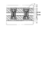
【解決手段】 第1の基板(10)の表面に第1の電極(12)が形成されている。第1の基板の表面上に、第1の電極の位置に第1の開口(20a)が形成されている絶縁膜(20)が配置されている。第1の開口内に、第1の電極に電気的に接続された金属部材(21)が形成されている。複数のカーボンナノチューブ(55)の一方の端部が金属部材内に埋め込まれ、金属部材に固定されている。
【選択図】 図1−4
Description
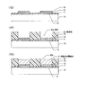
表面に第1の電極が形成された第1の基板と、
前記第1の基板の表面上に配置され、前記第1の電極の位置に第1の開口が形成されている絶縁膜と、
前記第1の開口内に形成され、前記第1の電極に電気的に接続された金属部材と、
一方の端部が前記金属部材内に埋め込まれ、該金属部材に固定されている複数のカーボンナノチューブと
を有する。
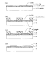
表面に第1の電極が形成された第1の基板の該表面の上に絶縁膜を配置する工程と、
前記絶縁膜の、前記第1の電極に対応する位置に第1の開口を形成する工程と、
前記第1の開口内に金属部材を形成する工程と、
前記第1の開口内の金属部材を溶融させた状態で、該金属部材に複数のカーボンナノチューブの一方の端部を挿入する工程と、
前記カーボンナノチューブが前記金属部材に挿入された状態で、該金属部材を固化させて、該カーボンナノチューブを該金属部材に固定する工程と
を有する。
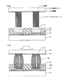
11 ソルダーレジスト
12 電極
15 シード層
16 レジストパターン
16a 開口
18 下地金属膜
20 絶縁膜
20a 開口
21 低融点金属部材
50 半導体チップ
51 電極
52 保護膜
55 カーボンナノチューブ
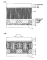
60 絞り膜
60a 開口
70 絶縁膜
71 シード層
72 下地金属膜
73 低融点金属部材
80 成長用仮基板
81 Al膜
82 Fe膜
90、91 絞り膜
Claims (6)
- 表面に第1の電極が形成された第1の基板と、
前記第1の基板の表面上に配置され、前記第1の電極の位置に第1の開口が形成されている絶縁膜と、
前記第1の開口内に形成され、前記第1の電極に電気的に接続された金属部材と、
一方の端部が前記金属部材内に埋め込まれ、該金属部材に固定されている複数のカーボンナノチューブと
を有する電子部品。 - さらに、前記絶縁膜の上に配置され、前記第1の開口に対応する位置に、該第1の開口よりも小さな第2の開口が形成された膜を有し、
前記カーボンナノチューブが、前記第2の開口を貫通している請求項1に記載の電子部品。 - さらに、
前記第1の基板の、前記第1の電極が形成された面に対向するように配置され、該第1の電極に対応する位置に第2の電極が形成された第2の基板を有し、
前記カーボンナノチューブの他方の端部が前記第2の電極に固定されている請求項1または2に記載の電子部品。 - さらに、前記カーボンナノチューブの、前記金属部材に埋め込まれている先端に形成された金属炭化物を有する請求項1乃至3のいずれか1項に記載の電子部品。
- 表面に第1の電極が形成された第1の基板の該表面の上に絶縁膜を配置する工程と、
前記絶縁膜の、前記第1の電極に対応する位置に第1の開口を形成する工程と、
前記第1の開口内に金属部材を形成する工程と、
前記第1の開口内の金属部材を溶融させた状態で、該金属部材に複数のカーボンナノチューブの一方の端部を挿入する工程と、
前記カーボンナノチューブが前記金属部材に挿入された状態で、該金属部材を固化させて、該カーボンナノチューブを該金属部材に固定する工程と
を有する電子部品の製造方法。 - 前記カーボンナノチューブを前記金属部材に挿入する前に、さらに、
第2の開口が設けられ、硬化時に収縮する熱硬化性樹脂で形成された膜を、該第2の開口が前記第1の開口に重なるように前記絶縁膜の上に配置する工程を有し、
前記カーボンナノチューブを前記金属部材に挿入する工程において、該カーボンナノチューブを前記第2の開口を通して該金属部材に挿入し、
前記カーボンナノチューブを前記金属部材に挿入した後、前記金属部材が溶融している状態で、前記膜を硬化させる工程を含み
前記膜が硬化した後の前記第2の開口が、前記第1の開口よりも小さくなっている請求項5に記載の電子部品の製造方法。
Priority Applications (1)
| Application Number | Priority Date | Filing Date | Title |
|---|---|---|---|
| JP2008236221A JP5186662B2 (ja) | 2008-09-16 | 2008-09-16 | 電子部品及び電子部品の製造方法 |
Applications Claiming Priority (1)
| Application Number | Priority Date | Filing Date | Title |
|---|---|---|---|
| JP2008236221A JP5186662B2 (ja) | 2008-09-16 | 2008-09-16 | 電子部品及び電子部品の製造方法 |
Publications (2)
| Publication Number | Publication Date |
|---|---|
| JP2010073725A true JP2010073725A (ja) | 2010-04-02 |
| JP5186662B2 JP5186662B2 (ja) | 2013-04-17 |
Family
ID=42205277
Family Applications (1)
| Application Number | Title | Priority Date | Filing Date |
|---|---|---|---|
| JP2008236221A Active JP5186662B2 (ja) | 2008-09-16 | 2008-09-16 | 電子部品及び電子部品の製造方法 |
Country Status (1)
| Country | Link |
|---|---|
| JP (1) | JP5186662B2 (ja) |
Cited By (3)
| Publication number | Priority date | Publication date | Assignee | Title |
|---|---|---|---|---|
| JP2012076938A (ja) * | 2010-09-30 | 2012-04-19 | Nippon Valqua Ind Ltd | 垂直配向カーボンナノチューブの成長密度制御方法 |
| WO2013114587A1 (ja) * | 2012-02-01 | 2013-08-08 | パイオニア株式会社 | 基板デバイスの製造方法及び基板デバイス |
| JP2020094940A (ja) * | 2018-12-13 | 2020-06-18 | 富士通株式会社 | 磁気センサ、及び磁気センサの製造方法 |
Citations (2)
| Publication number | Priority date | Publication date | Assignee | Title |
|---|---|---|---|---|
| JP2005109465A (ja) * | 2003-09-12 | 2005-04-21 | Semiconductor Energy Lab Co Ltd | 半導体装置、及びその作製方法 |
| WO2007123778A1 (en) * | 2006-03-31 | 2007-11-01 | Intel Corporation | Carbon nanotube-solder composite structures for interconnects, process of making same, packages containing same, and systems containing same |
-
2008
- 2008-09-16 JP JP2008236221A patent/JP5186662B2/ja active Active
Patent Citations (2)
| Publication number | Priority date | Publication date | Assignee | Title |
|---|---|---|---|---|
| JP2005109465A (ja) * | 2003-09-12 | 2005-04-21 | Semiconductor Energy Lab Co Ltd | 半導体装置、及びその作製方法 |
| WO2007123778A1 (en) * | 2006-03-31 | 2007-11-01 | Intel Corporation | Carbon nanotube-solder composite structures for interconnects, process of making same, packages containing same, and systems containing same |
Cited By (4)
| Publication number | Priority date | Publication date | Assignee | Title |
|---|---|---|---|---|
| JP2012076938A (ja) * | 2010-09-30 | 2012-04-19 | Nippon Valqua Ind Ltd | 垂直配向カーボンナノチューブの成長密度制御方法 |
| WO2013114587A1 (ja) * | 2012-02-01 | 2013-08-08 | パイオニア株式会社 | 基板デバイスの製造方法及び基板デバイス |
| JP2020094940A (ja) * | 2018-12-13 | 2020-06-18 | 富士通株式会社 | 磁気センサ、及び磁気センサの製造方法 |
| JP7147533B2 (ja) | 2018-12-13 | 2022-10-05 | 富士通株式会社 | 磁気センサ、及び磁気センサの製造方法 |
Also Published As
| Publication number | Publication date |
|---|---|
| JP5186662B2 (ja) | 2013-04-17 |
Similar Documents
| Publication | Publication Date | Title |
|---|---|---|
| US7851928B2 (en) | Semiconductor device having substrate with differentially plated copper and selective solder | |
| JP5347222B2 (ja) | 半導体装置の製造方法 | |
| US8563363B2 (en) | Fabricating method of semiconductor package structure | |
| JP2014038993A (ja) | コア基板及びこれを用いたプリント回路基板 | |
| JPWO2013027718A1 (ja) | 部品実装プリント基板及びその製造方法 | |
| KR100860533B1 (ko) | 금속 인쇄회로기판 제조방법 | |
| KR20110029465A (ko) | 인쇄회로기판 및 그의 제조 방법 | |
| US10062623B2 (en) | Semiconductor package substrate, package system using the same and method for manufacturing thereof | |
| JP5186662B2 (ja) | 電子部品及び電子部品の製造方法 | |
| JP2004266074A (ja) | 配線基板 | |
| JP2010157693A (ja) | 金属バンプを備えた半導体パッケージ基板 | |
| CN102376677B (zh) | 半导体封装结构及半导体封装结构的制作方法 | |
| JP2011146510A (ja) | 部品内蔵基板および電子回路モジュール | |
| KR100744149B1 (ko) | 은 범프를 이용한 반도체 패키지 구조 및 형성 방법 | |
| JP2010219397A (ja) | 電子部品及びその製造方法 | |
| JP2010118469A (ja) | 半導体装置及びその製造方法 | |
| JP5267540B2 (ja) | 半導体装置 | |
| CN108461405B (zh) | 线路载板及其制造方法 | |
| JPS63222437A (ja) | 電気回路部材 | |
| JP2016100352A (ja) | プリント配線板およびその製造方法 | |
| JP5493020B2 (ja) | 配線基板の製造方法及び半導体パッケージの製造方法 | |
| US20130277850A1 (en) | Electronic device | |
| WO2018003391A1 (ja) | 部品内蔵基板及びその製造方法、並びに高周波モジュール | |
| JP2002270711A (ja) | 半導体装置用配線基板およびその製造方法 | |
| JP2005302968A (ja) | 配線基板 |
Legal Events
| Date | Code | Title | Description |
|---|---|---|---|
| A621 | Written request for application examination |
Free format text: JAPANESE INTERMEDIATE CODE: A621 Effective date: 20101119 |
|
| A977 | Report on retrieval |
Free format text: JAPANESE INTERMEDIATE CODE: A971007 Effective date: 20120126 |
|
| A131 | Notification of reasons for refusal |
Free format text: JAPANESE INTERMEDIATE CODE: A131 Effective date: 20121002 |
|
| A521 | Request for written amendment filed |
Free format text: JAPANESE INTERMEDIATE CODE: A523 Effective date: 20121121 |
|
| TRDD | Decision of grant or rejection written | ||
| A01 | Written decision to grant a patent or to grant a registration (utility model) |
Free format text: JAPANESE INTERMEDIATE CODE: A01 Effective date: 20121211 |
|
| A61 | First payment of annual fees (during grant procedure) |
Free format text: JAPANESE INTERMEDIATE CODE: A61 Effective date: 20121224 |
|
| FPAY | Renewal fee payment (event date is renewal date of database) |
Free format text: PAYMENT UNTIL: 20160201 Year of fee payment: 3 |
|
| R150 | Certificate of patent or registration of utility model |
Ref document number: 5186662 Country of ref document: JP Free format text: JAPANESE INTERMEDIATE CODE: R150 Free format text: JAPANESE INTERMEDIATE CODE: R150 |