JP2010067863A - Light emitting device, and light emitting module - Google Patents
Light emitting device, and light emitting module Download PDFInfo
- Publication number
- JP2010067863A JP2010067863A JP2008233986A JP2008233986A JP2010067863A JP 2010067863 A JP2010067863 A JP 2010067863A JP 2008233986 A JP2008233986 A JP 2008233986A JP 2008233986 A JP2008233986 A JP 2008233986A JP 2010067863 A JP2010067863 A JP 2010067863A
- Authority
- JP
- Japan
- Prior art keywords
- light emitting
- light
- emitting element
- resin
- emitting device
- Prior art date
- Legal status (The legal status is an assumption and is not a legal conclusion. Google has not performed a legal analysis and makes no representation as to the accuracy of the status listed.)
- Granted
Links
Images


Classifications
-
- H—ELECTRICITY
- H01—ELECTRIC ELEMENTS
- H01L—SEMICONDUCTOR DEVICES NOT COVERED BY CLASS H10
- H01L2224/00—Indexing scheme for arrangements for connecting or disconnecting semiconductor or solid-state bodies and methods related thereto as covered by H01L24/00
- H01L2224/01—Means for bonding being attached to, or being formed on, the surface to be connected, e.g. chip-to-package, die-attach, "first-level" interconnects; Manufacturing methods related thereto
- H01L2224/42—Wire connectors; Manufacturing methods related thereto
- H01L2224/44—Structure, shape, material or disposition of the wire connectors prior to the connecting process
- H01L2224/45—Structure, shape, material or disposition of the wire connectors prior to the connecting process of an individual wire connector
- H01L2224/45001—Core members of the connector
- H01L2224/45099—Material
- H01L2224/451—Material with a principal constituent of the material being a metal or a metalloid, e.g. boron (B), silicon (Si), germanium (Ge), arsenic (As), antimony (Sb), tellurium (Te) and polonium (Po), and alloys thereof
- H01L2224/45138—Material with a principal constituent of the material being a metal or a metalloid, e.g. boron (B), silicon (Si), germanium (Ge), arsenic (As), antimony (Sb), tellurium (Te) and polonium (Po), and alloys thereof the principal constituent melting at a temperature of greater than or equal to 950°C and less than 1550°C
- H01L2224/45144—Gold (Au) as principal constituent
-
- H—ELECTRICITY
- H01—ELECTRIC ELEMENTS
- H01L—SEMICONDUCTOR DEVICES NOT COVERED BY CLASS H10
- H01L2224/00—Indexing scheme for arrangements for connecting or disconnecting semiconductor or solid-state bodies and methods related thereto as covered by H01L24/00
- H01L2224/01—Means for bonding being attached to, or being formed on, the surface to be connected, e.g. chip-to-package, die-attach, "first-level" interconnects; Manufacturing methods related thereto
- H01L2224/42—Wire connectors; Manufacturing methods related thereto
- H01L2224/47—Structure, shape, material or disposition of the wire connectors after the connecting process
- H01L2224/48—Structure, shape, material or disposition of the wire connectors after the connecting process of an individual wire connector
- H01L2224/4805—Shape
- H01L2224/4809—Loop shape
- H01L2224/48091—Arched
-
- H—ELECTRICITY
- H01—ELECTRIC ELEMENTS
- H01L—SEMICONDUCTOR DEVICES NOT COVERED BY CLASS H10
- H01L2224/00—Indexing scheme for arrangements for connecting or disconnecting semiconductor or solid-state bodies and methods related thereto as covered by H01L24/00
- H01L2224/01—Means for bonding being attached to, or being formed on, the surface to be connected, e.g. chip-to-package, die-attach, "first-level" interconnects; Manufacturing methods related thereto
- H01L2224/42—Wire connectors; Manufacturing methods related thereto
- H01L2224/47—Structure, shape, material or disposition of the wire connectors after the connecting process
- H01L2224/48—Structure, shape, material or disposition of the wire connectors after the connecting process of an individual wire connector
- H01L2224/481—Disposition
- H01L2224/48151—Connecting between a semiconductor or solid-state body and an item not being a semiconductor or solid-state body, e.g. chip-to-substrate, chip-to-passive
- H01L2224/48221—Connecting between a semiconductor or solid-state body and an item not being a semiconductor or solid-state body, e.g. chip-to-substrate, chip-to-passive the body and the item being stacked
- H01L2224/48245—Connecting between a semiconductor or solid-state body and an item not being a semiconductor or solid-state body, e.g. chip-to-substrate, chip-to-passive the body and the item being stacked the item being metallic
- H01L2224/48247—Connecting between a semiconductor or solid-state body and an item not being a semiconductor or solid-state body, e.g. chip-to-substrate, chip-to-passive the body and the item being stacked the item being metallic connecting the wire to a bond pad of the item
-
- H—ELECTRICITY
- H01—ELECTRIC ELEMENTS
- H01L—SEMICONDUCTOR DEVICES NOT COVERED BY CLASS H10
- H01L2224/00—Indexing scheme for arrangements for connecting or disconnecting semiconductor or solid-state bodies and methods related thereto as covered by H01L24/00
- H01L2224/01—Means for bonding being attached to, or being formed on, the surface to be connected, e.g. chip-to-package, die-attach, "first-level" interconnects; Manufacturing methods related thereto
- H01L2224/42—Wire connectors; Manufacturing methods related thereto
- H01L2224/47—Structure, shape, material or disposition of the wire connectors after the connecting process
- H01L2224/49—Structure, shape, material or disposition of the wire connectors after the connecting process of a plurality of wire connectors
- H01L2224/491—Disposition
- H01L2224/4911—Disposition the connectors being bonded to at least one common bonding area, e.g. daisy chain
- H01L2224/49113—Disposition the connectors being bonded to at least one common bonding area, e.g. daisy chain the connectors connecting different bonding areas on the semiconductor or solid-state body to a common bonding area outside the body, e.g. converging wires
Abstract
Description
本発明は、発光素子を用いた発光装置、発光モジュールに関する。 The present invention relates to a light emitting device and a light emitting module using a light emitting element.
近年、携帯電話機の液晶ディスプレイのバックライトに白色LED(LED:Light Emitting Diode)が採用されたことにより、白色LEDの生産量が飛躍的に拡大している。ここで、白色LEDのパッケージとは、半導体発光素子(LED)を備えた発光装置のことであって、例えば凹部を有する白色樹脂ケースの凹部内側にリードフレームを露出させるように配置し、凹部の内側に露出するリードフレームに半導体発光素子を取り付けるとともにこれらを電気的に接続し、半導体発光素子を覆うように、凹部に蛍光体を含有させた封止樹脂を形成してなるものである。今後、携帯電話機以外の用途でも、液晶ディスプレイのバックライトに白色LEDの使用が広まっていくことが期待されている。また、液晶ディスプレイのバックライトへの使用量が増えるに伴って、他の照明分野でも採用が検討されている。今後、携帯電話機以外の用途でも液晶ディスプレイのバックライトに白色LEDが使われることは確実と思われる。液晶ディスプレイのバックライトへの使用量が増えるに伴って他の照明分野でも採用が検討されている。 2. Description of the Related Art In recent years, white LED (Light Emitting Diode) has been adopted as a backlight of a liquid crystal display of a mobile phone, and the production amount of white LEDs has been dramatically increased. Here, the white LED package is a light emitting device including a semiconductor light emitting element (LED), and is disposed so as to expose the lead frame inside the concave portion of the white resin case having the concave portion, for example. A semiconductor light emitting element is attached to the lead frame exposed to the inside, and these are electrically connected, and a sealing resin containing a phosphor is formed in the concave portion so as to cover the semiconductor light emitting element. In the future, it is expected that the use of white LEDs for the backlight of liquid crystal displays will be widespread even in applications other than mobile phones. In addition, as the amount of liquid crystal display used as a backlight increases, adoption in other lighting fields is also being studied. In the future, it seems to be certain that white LEDs will be used for the backlight of liquid crystal displays in applications other than mobile phones. As the amount of liquid crystal displays used as backlights increases, adoption in other lighting fields is also being considered.
液晶ディスプレイのバックライトに白色LEDを使う場合、大画面をできるだけ少ない電力で規定の輝度を得るために、白色LEDを搭載したパッケージの高効率化がきわめて強く要求されている。さらに、液晶ディスプレイの表示面全体における色のばらつきについても、厳しい規格が存在する。例えばCIEのYxy表色系の色度の範囲として規定すると、x、yそれぞれにおいて±0.008程度のばらつきに抑制することが要求されている。ディスプレイの表示面全体における色のばらつきを前述の範囲内に収めるためには、パッケージについても、その範囲に入れる必要がある。 When a white LED is used as a backlight of a liquid crystal display, in order to obtain a specified luminance with a power as small as possible on a large screen, a highly efficient package equipped with the white LED is extremely demanded. Furthermore, there are strict standards for color variations across the display surface of a liquid crystal display. For example, if it is defined as the chromaticity range of the CIE Yxy color system, it is required to suppress variations of about ± 0.008 in each of x and y. In order to keep the color variation on the entire display surface of the display within the above-mentioned range, the package needs to be within the range.
ハンドラーテスターなどで一つ一つ測定して要求範囲からずれているパッケージを発見した場合は、そのパッケージを取り除かなければならない。よって、パッケージのコストは、すべてのパッケージを要求される色度の範囲に入れないと、その分だけ上がってしまう。逆を言うと白色LEDを用いた照明(バックライトも含む)を普及させるためには、白色LEDのパッケージのコストを下げる必要があり、そのためにはパッケージの製造工程で輝度低下の原因を極力排除するとともに色のばらつきを極力減らすことが要求されている。 If you find a package that deviates from the required range by measuring it with a handler tester, you must remove the package. Thus, the cost of the package will increase by that amount unless all packages are within the required chromaticity range. In other words, in order to popularize lighting using white LEDs (including backlights), it is necessary to reduce the cost of the white LED package. To that end, the cause of the brightness reduction is eliminated as much as possible in the package manufacturing process. In addition, it is required to reduce the color variation as much as possible.
ところで、白色LEDのパッケージにおいては、半導体発光素子で発生した光がすべて有効に使われているわけではなく、パッケージ内部に閉じ込められて、出て来られない部分がかなりある。封止樹脂は一般に1.4〜1.5の屈折率があり、空気は1であるから、屈折率の違いにより一定の入射角以下で入射した光は反射して元に戻る。球面の中心に発光体(例えば半導体発光素子)があると仮定すると、発光体から出力されるすべての光は、境界面に対して直角に入射するので反射されることが無く、光の取り出し効率が最も高いといわれている。そこで、半球状のレンズをつくりその中心に発光体を配置する発光装置(パッケージ)が数多く提案されている。 By the way, in the white LED package, not all the light generated in the semiconductor light emitting element is effectively used, and there are quite a portion that is confined inside the package and cannot come out. Since the sealing resin generally has a refractive index of 1.4 to 1.5 and air is 1, light incident at a certain incident angle or less is reflected and returned to the original due to the difference in refractive index. Assuming that there is a light emitter (for example, a semiconductor light-emitting element) at the center of the spherical surface, all light output from the light emitter is incident at a right angle to the boundary surface and is not reflected, and light extraction efficiency Is said to be the highest. Thus, many light emitting devices (packages) have been proposed in which a hemispherical lens is formed and a light emitter is arranged at the center thereof.
ところが、実際に発光装置を試作してみると、そのような構造では十分な発光効率を得ることができず、方向ごとに色度のばらつきも大きく、パッケージ間での色度のばらつきも実用に耐えるものはできなかった。色のばらつきには2種類あり、パッケージごとに色度が異なる場合と、一つのパッケージで方向(位置)に応じて色度が異なる場合とがある。そこで、光の取り出し効率を極限まで向上させるとともに、これら2種類の色のばらつきを抑える技術が、いろいろと提案されてきている(特許文献1〜4参照)。 However, when a prototype of a light-emitting device is actually manufactured, such a structure does not provide sufficient luminous efficiency, chromaticity varies greatly from direction to direction, and chromaticity variation between packages is practical. I couldn't do anything to endure. There are two types of color variations, and there are cases where the chromaticity varies from package to package and chromaticity varies depending on the direction (position) of one package. Thus, various techniques have been proposed for improving the light extraction efficiency to the limit and suppressing variations in these two types of colors (see Patent Documents 1 to 4).
さらに、パッケージから出力される光の色度が時間とともに変化してしまうと、規格から外れてしまうので、時間とともに輝度や色度が変化するのを極力抑える必要がある。したがって、リフレクタが形成される樹脂容器の樹脂材料および封止樹脂については、リードフレームのメッキ表面の変色を押さえ込むために十分な検討が必要とされる。 Furthermore, if the chromaticity of the light output from the package changes with time, it deviates from the standard, so it is necessary to suppress the change in luminance and chromaticity with time as much as possible. Therefore, sufficient study is required for the resin material and the sealing resin of the resin container in which the reflector is formed in order to suppress discoloration of the plating surface of the lead frame.
特許文献1及び特許文献2では、一つのパッケージで方向により色度が異なることを防ぐために以下の記述がある。すなわち、発光素子から発光装置の光取り出し面までに存在する蛍光体を含有した樹脂の層の厚さが一定であることを必須の要件としている。これを達成するために特殊な形状のパッケージにするとか封止樹脂を2層に分けて、蛍光体含有の層で発光素子を均一の厚さで覆うことかパッケージの外周に均一の厚さの蛍光体含有封止樹脂を塗りつけるようなことをする必要がある。
In Patent Document 1 and
そこで、特許文献3には、主に方向によって色度がばらつくのを防ぐのを目的として、次の方法が提案されている。すなわち、白色パッケージ容器に封止樹脂を注入すると蛍光体が部分的に沈んでしまい、発光している半導体発光素子から封止樹脂の光が通過する距離を一定にできないので、方向により色度がばらつくとして、蛍光体を含んだ層を粒子が沈降しない電気泳動法などの別な方法で作成し、蛍光体を含んだ層の厚さを均一にすることが提案されている。
Therefore,
一方、特許文献4では、上記とは異なる手法で、1つのパッケージで方向によって発光色がばらつくことを防ぐことが提案されている。すなわち、蛍光体を封止樹脂に均一に分散することで、1つのパッケージで方向によって色度がばらつくことを防げるとしている。しかし、特許文献1、2、3の記述のように発光素子から出た光が封止樹脂を通って外に出るまでの距離が異なるパッケージでは、封止樹脂に蛍光体を均一に分散しただけでは、2つあるばらつき要因のうち、パッケージ間の色度のばらつきを抑えるのに効果はあるが、1つのパッケージで方向によって色度がばらつくのを抑えることはできない。
On the other hand,
また、仮に封止樹脂に蛍光体を均一分散させたとしても、1つの発光素子を覆う蛍光体含有封止樹脂層の厚みがばらつくと、1つのパッケージで方向によって発光色がばらつく原因となる。さらに、パッケージごとに蛍光体を含んだ層の厚さが異なると、パッケージごとに色度がばらつくことになる。パッケージごとに色度がばらつくことに関しては、それを防ぐ方法に対する明確な記述はないが、実際には、発光素子を覆う蛍光体含有封止樹脂層の厚みを極力同じにすることが前提条件になっているものと考えられる。
LED等の発光素子を利用した照明は、液晶ディスプレイのバックライトとして採用されたのを需要の中心として発展してきている。しかしながら、現状では、携帯電話機向けの小型のディスプレイが主体であり、パソコン用モニタや大型TVなどの大面積の液晶ディスプレイ用には、ほとんど採用されていない。これは、上述したように、輝度が十分でなかったり、色のばらつきに対する安定性、輝度・色座の経時的変化に対する安定性が十分確保されていなかったりするためである。 Illumination using light emitting elements such as LEDs has been developed mainly as a demand for backlights used in liquid crystal displays. However, at present, small displays for cellular phones are mainly used, and are hardly adopted for large area liquid crystal displays such as monitors for personal computers and large TVs. This is because, as described above, the luminance is not sufficient, the stability against color variations, and the stability against changes with time in luminance and color constellation are not sufficiently ensured.
携帯電話機等の液晶ディスプレイの場合は、色再現範囲がNTSC比で70%程度でも実用上問題ないので、黄色蛍光体と青色LEDとの組合せで白色を発色させるのが一般的である。これに対し、大型液晶テレビの場合は、最低でもNTSC比で82%以上の色再現範囲が要求されている。これを達成するためには、黄色一種類の蛍光体では難しく、青色の光で緑色に発光する緑色蛍光体と、赤色に発光する赤色蛍光体とを混ぜて使用する必要がある。このように2種類の蛍光体を用いた場合、各蛍光体が均一に分散していない限り、発光装置毎の色度のばらつきと、同じ発光装置内でも方向によって色度が変動してしまう問題がますます深刻になる。 In the case of a liquid crystal display such as a mobile phone, there is no practical problem even if the color reproduction range is about 70% in terms of NTSC ratio. Therefore, it is common to develop a white color with a combination of a yellow phosphor and a blue LED. On the other hand, in the case of a large-sized liquid crystal television, a color reproduction range of 82% or more is required at least as compared with NTSC. In order to achieve this, it is difficult to use a single yellow phosphor, and it is necessary to use a mixture of a green phosphor that emits green light with blue light and a red phosphor that emits red light. When two types of phosphors are used in this way, unless the phosphors are uniformly dispersed, the chromaticity varies among the light emitting devices and the chromaticity varies depending on the direction within the same light emitting device. Will become more and more serious.
ところが一般に、緑色蛍光体と赤色蛍光体とでは密度、粒度分布とも異なるので、沈降速度に差があり、発光色の色度が変化してしまう。1つの発光装置の方向による色度のばらつきと発光装置毎の色度のばらつきとを極力小さくし、液晶表示装置のバックライトに要求される規格である、色度x,yともに±0.008以内に95%以上を入れるための製造技術が必要となる。 However, since the green phosphor and the red phosphor generally have different densities and particle size distributions, there is a difference in sedimentation speed, and the chromaticity of the emission color changes. The variation in chromaticity depending on the direction of one light emitting device and the variation in chromaticity for each light emitting device are minimized, and both chromaticity x and y, which are standards required for a backlight of a liquid crystal display device, are ± 0.008. Manufacturing technology is required to put 95% or more in the inside.
また、半導体発光素子と蛍光体とを組み合わせて構成したパッケージでは、半導体発光素子を搭載する位置によって、出力される光の色度にばらつきが生じることがある。例えば、半導体発光素子に近い側では蛍光体の発光色よりも半導体発光素子の発光色が強くなり、半導体発光素子から遠い側では半導体発光素子の発光色が弱まる分、蛍光体の発光色が強くなる傾向がある。 Further, in a package configured by combining a semiconductor light emitting element and a phosphor, chromaticity of output light may vary depending on a position where the semiconductor light emitting element is mounted. For example, the emission color of the semiconductor light emitting element is stronger than the emission color of the phosphor on the side closer to the semiconductor light emitting element, and the emission color of the phosphor is stronger because the emission color of the semiconductor light emitting element is weaker on the side farther from the semiconductor light emitting element. Tend to be.
本発明は、発光素子から出力される光を、蛍光体を用いて波長変換を行う発光装置において、出力される光の色のばらつきを抑制しつつ、発光素子の配置の自由度を高めることを目的とする。 The present invention provides a light-emitting device that converts the wavelength of light output from a light-emitting element using a phosphor, and increases the degree of freedom in arranging the light-emitting elements while suppressing variations in the color of the output light. Objective.
かかる目的のもと、本発明が適用される発光装置は、底面と、底面の周縁から立ち上がる壁面とを含む凹部を備えた樹脂容器と、金属導体と、金属導体の表面に形成された0.3以上且つ1.0以下の光沢度を有する銀メッキ層とを有し、樹脂容器の凹部の底面に露出した状態で配置される導体部と、凹部の底面において、底面の中心位置とは異なる位置に取り付けられ、導体部と電気的に接続される発光素子と、発光素子の発光波長に対して透明な透明樹脂と、透明樹脂に分散され発光素子の発光波長をより長波長の光に変換する蛍光体とを含み、凹部において発光素子を封止する封止樹脂とを含んでいる。 For such a purpose, a light emitting device to which the present invention is applied includes a resin container provided with a recess including a bottom surface and a wall surface rising from the peripheral edge of the bottom surface, a metal conductor, and a surface formed on the surface of the metal conductor. And a silver plating layer having a glossiness of 3 or more and 1.0 or less, and the conductor portion disposed in a state exposed on the bottom surface of the recess of the resin container is different from the center position of the bottom surface of the recess. A light emitting element that is attached to a position and is electrically connected to a conductor, a transparent resin that is transparent to the light emitting wavelength of the light emitting element, and dispersed in the transparent resin to convert the light emitting wavelength of the light emitting element into longer wavelength light And a sealing resin for sealing the light emitting element in the recess.
このような発光装置において、導体部は、0.3以上且つ1.0以下の光沢度を有する銀メッキ層によって得られるランバーシアン型の反射特性によって発光素子からの光を反射させることを特徴とすることができる。
また、樹脂容器が、白色顔料を用いて白色化されていることを特徴とすることができる。
さらに、導体部における銀メッキ層の光沢度が、0.5以上且つ0.7以下であることを特徴とすることができる。
さらにまた、発光素子は青色光を出力し、蛍光体は、青色光を緑色光に変換して出力する第1の蛍光体と、青色光を赤色光に変換して出力する第2の蛍光体とを含むことを特徴とすることができる。
また、透明樹脂が、シリコン樹脂にて構成されることを特徴とすることができる。
そして、封止樹脂は、発光素子から出力される光を外部に出射する出射面を有し、出射面は、樹脂容器との境界部側から中央部側に向けて凹む凹状の形状を有し、出射面の凹み量が、20μm以上且つ100μm以下の範囲に設定されることを特徴とすることができる。
In such a light emitting device, the conductor portion reflects light from the light emitting element by a Lambertian reflection characteristic obtained by a silver plating layer having a glossiness of 0.3 or more and 1.0 or less. can do.
The resin container may be whitened using a white pigment.
Furthermore, the glossiness of the silver plating layer in a conductor part can be characterized by being 0.5 or more and 0.7 or less.
Furthermore, the light emitting element outputs blue light, and the phosphor is a first phosphor that converts blue light into green light and outputs it, and a second phosphor that converts blue light into red light and outputs it. It can be characterized by including.
Further, the transparent resin may be composed of a silicon resin.
The sealing resin has an emission surface that emits the light output from the light emitting element to the outside, and the emission surface has a concave shape that is recessed from the boundary side to the center side with the resin container. The depression amount of the exit surface is set in a range of 20 μm or more and 100 μm or less.
また、他の観点から捉えると、本発明が適用される発光装置は、凹部を有する樹脂容器と、金属導体と、金属導体の表面に形成された0.3以上且つ1.0以下の光沢度を有する銀メッキ層とを有し、樹脂容器の凹部の内側に露出した状態で形成される導体部と、凹部の内側に設けられ、導体部と電気的に接続される複数の発光素子と、複数の発光素子の発光波長に対して透明な透明樹脂と、透明樹脂に分散され発光素子の発光波長をより長波長の光に変換する蛍光体とを含み、凹部において複数の発光素子を封止する封止樹脂とを含んでいる。 From another point of view, the light emitting device to which the present invention is applied includes a resin container having a recess, a metal conductor, and a glossiness of 0.3 or more and 1.0 or less formed on the surface of the metal conductor. A conductor part formed in a state exposed to the inside of the recess of the resin container, a plurality of light emitting elements provided inside the recess and electrically connected to the conductor part, A transparent resin transparent to the emission wavelengths of a plurality of light emitting elements, and a phosphor dispersed in the transparent resin that converts the light emission wavelength of the light emitting elements into light having a longer wavelength, and sealing the plurality of light emitting elements in the recesses Sealing resin.
このような発光装置において、導体部は、0.3以上且つ1.0以下の光沢度を有する銀メッキ層によって得られるランバーシアン型の反射特性によって発光素子からの光を反射させることを特徴とすることができる。
また、樹脂容器は、チタニア微粒子を含む樹脂にて構成されることを特徴とすることができる。
さらに、導体部における銀メッキ層の光沢度が、0.5以上且つ0.7以下であることを特徴とすることができる。
さらにまた、可視領域における樹脂容器および導体部の銀メッキ層の光反射率が85%以上98%以下であることを特徴とすることができる。
そして、凹部の底面に露出する導体部の面積が、底面の全面積の半分以上に設定されることを特徴とすることができる。
In such a light emitting device, the conductor portion reflects light from the light emitting element by a Lambertian reflection characteristic obtained by a silver plating layer having a glossiness of 0.3 or more and 1.0 or less. can do.
Further, the resin container may be formed of a resin containing titania fine particles.
Furthermore, the glossiness of the silver plating layer in a conductor part can be characterized by being 0.5 or more and 0.7 or less.
Furthermore, the light reflectance of the resin container and the silver plating layer of the conductor in the visible region may be 85% or more and 98% or less.
And the area of the conductor part exposed to the bottom face of a recessed part can be set to the half or more of the total area of a bottom face, It can be characterized by the above-mentioned.
さらに、他の観点から捉えると、本発明が適用される発光モジュールは、基板と、基板に取り付けられる複数の発光装置とを備え、発光装置は、底面と、底面の周縁から立ち上がる壁面とを含む凹部を備えた樹脂容器と、金属導体と、金属導体の表面に形成された0.3以上且つ1.0以下の光沢度を有する銀メッキ層とを有し、樹脂容器の凹部の底面に露出した状態で配置される導体部と、凹部の底面において、底面の中心位置とは異なる位置に取り付けられ、導体部と電気的に接続される発光素子と、発光素子の発光波長に対して透明な透明樹脂と、透明樹脂に分散され発光素子の発光波長をより長波長の光に変換する蛍光体とを含み、凹部において発光素子を封止する封止樹脂とを有することを特徴としている。 Further, from another viewpoint, the light emitting module to which the present invention is applied includes a substrate and a plurality of light emitting devices attached to the substrate, and the light emitting device includes a bottom surface and a wall surface rising from a peripheral edge of the bottom surface. A resin container having a recess, a metal conductor, and a silver plating layer having a glossiness of 0.3 to 1.0 formed on the surface of the metal conductor and exposed to the bottom surface of the recess of the resin container A light emitting element that is attached to a position different from the center position of the bottom surface, and is transparent to the light emission wavelength of the light emitting element. It includes a transparent resin and a phosphor that is dispersed in the transparent resin and converts the emission wavelength of the light emitting element into light having a longer wavelength, and has a sealing resin that seals the light emitting element in the recess.
このような発光モジュールにおいて、発光装置の導体部は、0.3以上且つ1.0以下の光沢度を有する銀メッキ層によって得られるランバーシアン型の反射特性によって発光素子からの光を反射させることを特徴とすることができる。
また、発光装置の樹脂容器が、白色顔料を用いて白色化されていることを特徴とすることができる。
さらに、発光装置の導体部における銀メッキ層の光沢度が、0.5以上且つ0.7以下であることを特徴とすることができる。
In such a light emitting module, the conductor portion of the light emitting device reflects light from the light emitting element by a Lambertian reflection characteristic obtained by a silver plating layer having a glossiness of 0.3 or more and 1.0 or less. Can be characterized.
In addition, the resin container of the light emitting device may be whitened using a white pigment.
Furthermore, the glossiness of the silver plating layer in the conductor part of the light emitting device may be 0.5 or more and 0.7 or less.
本発明によれば、発光素子から出力される光を、蛍光体を用いて波長変換を行う発光装置において、出力される光の色のばらつきを抑制しつつ、発光素子の配置の自由度を高めることができる。 According to the present invention, in a light-emitting device that performs wavelength conversion of light output from a light-emitting element using a phosphor, the degree of freedom in arrangement of the light-emitting elements is increased while suppressing variations in the color of the output light. be able to.
以下、添付図面を参照して、本発明の実施の形態について詳細に説明する。
<実施の形態1>
図1は、本実施の形態が適用される液晶表示装置の全体構成を示す図である。この液晶表示装置は、液晶表示モジュール50と、この液晶表示モジュール50の背面側(図1では下部側)に設けられるバックライト装置10とを備えている。
Embodiments of the present invention will be described below in detail with reference to the accompanying drawings.
<Embodiment 1>
FIG. 1 is a diagram showing an overall configuration of a liquid crystal display device to which the present embodiment is applied. The liquid crystal display device includes a liquid
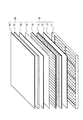
バックライト装置10は、バックライトフレーム11と、発光装置がそれぞれに配列され、バックライトフレーム11に収容される複数の発光モジュール12とを備えている。また、バックライト装置10は、光学フィルムの積層体として、面全体を均一な明るさとするために光を散乱・拡散させる板(またはフィルム)である拡散板13と、前方への集光効果を持たせたプリズムシート14、15とを備えている。また、輝度を向上させるための拡散・反射型の輝度向上フィルム16が、必要に応じて備えられる。
The
一方、液晶表示モジュール50は、2枚のガラス基板により液晶が挟まれて構成される液晶パネル51と、この液晶パネル51の各々のガラス基板に積層され、光波の振動をある方向に制限するための偏光板52、53とを備えている。更に、本液晶表示装置には、図示しない駆動用LSIなどの周辺部材も装着される。
On the other hand, the liquid
液晶パネル51は、図示しない各種構成要素を含んで構成されている。例えば、2枚のガラス基板に、図示しない表示電極、薄膜トランジスタ(TFT:Thin Film Transistor)などのアクティブ素子、液晶、スペーサ、シール剤、配向膜、共通電極、保護膜、カラーフィルタ等を備えている。
The
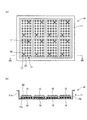
図2は、バックライト装置10の構造を説明するための図である。ここで、図2(a)は、発光モジュール12が装着されたバックライトフレーム11を、図1に示す液晶表示モジュール50側からみた上面図であり、図2(b)は図2(a)のIIB−IIB断面図である。本実施の形態では、液晶表示モジュール50の背面直下に光源を置く直下型のバックライト構造を採用している。そして、このバックライト構造では、液晶表示モジュール50の背面の全体に対してほぼ均等に、発光素子を有する発光装置60が配列されている。なお本実施の形態で用いる発光装置60は、一般的にLEDパッケージと呼ばれるものである。
FIG. 2 is a diagram for explaining the structure of the
バックライトフレーム11は、例えばアルミニウムやマグネシウム、鉄、またはそれらを含む金属合金などで生成される筐体構造を形成している。そして、その筐体構造の内側に、例えば白色高反射の性能を有するポリエステルフィルムなどが貼られ、リフレクタとしても機能するようになっている。この筐体構造としては、液晶表示モジュール50の大きさに対応して設けられる背面部11a、この背面部11aの四隅を囲う側面部11bを備えている。そして、この背面部11a上には放熱シート18を設けることができる。
The
図2に示す例では、発光モジュール12が複数(この例では8枚)設けられている。そして、各発光モジュール12は、それぞれ複数 (この例では1枚の発光モジュール12に対して2本) のネジ17により、放熱シート18を介してバックライトフレーム11に固定されている。
In the example shown in FIG. 2, a plurality of light emitting modules 12 (eight in this example) are provided. Each
発光モジュール12は、基板の一例としての配線基板20と、この配線基板20に実装される複数(この例では28個)の発光装置60とを備えている。なお、各発光装置60は、後述する構成を備えることにより、それぞれが白色光を出力するようになっている。
The
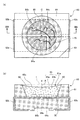
図3は、本実施の形態で用いられる発光装置60の構成を説明するための図である。ここで、図3(a)は発光装置60の上面図を、図3(b)は図3(a)のIIIB−IIIB断面図を、それぞれ示している。
FIG. 3 is a diagram for explaining the configuration of the
この発光装置60は、上部側に凹部61aが形成された樹脂容器61と、樹脂容器61と一体化したリードフレームからなる第1アノード用リード部62a、第2アノード用リード部62b、第3アノード用リード部62cおよびカソード用リード部63と、凹部61aの底面70に取り付けられた第1半導体発光素子64a、第2半導体発光素子64bおよび第3半導体発光素子64cと、凹部61aを覆うように設けられた封止樹脂65とを備えている。なお、図3(a)においては、封止樹脂65の記載を省略している。
The
樹脂容器61は、第1アノード用リード部62a、第2アノード用リード部62b、第3アノード用リード部62cおよびカソード用リード部63を含む金属リード部に、白色顔料が含有された熱可塑性樹脂(以下の説明では白色樹脂と呼ぶ)を射出成型することによって形成されている。
The
この樹脂容器61を構成する白色樹脂は、可視光の光反射率が85%以上であって98%以下となるように白色顔料の含有率、粒径等が調整されている。言い換えると、樹脂容器61の可視光の光吸収率が15%未満とされている。白色顔料としては、チタニア(酸化チタン)を微粒子化したものを用いることが好ましい。チタニアは、他の白色顔料に比べて屈折率が高く、また、光吸収率が低いので、本実施形態の樹脂容器61に好適に用いることができる。他の白色顔料、例えば酸化アルミニウムは、チタニアに比べて輝度が大幅に低下するので、チタニアと比較して好ましくない。ただし、チタニアは、光触媒作用があるので樹脂を変質させてしまうおそれがある。そこで、チタニアに対し、水酸化アルミニウムなどで表面処理を行うことが好ましい。この表面処理が十分でないと、樹脂容器61を構成する樹脂が変質して特定の波長を吸収するので、経時的な色度座標の変化が起こることがある。したがって、白色顔料としてのチタニアの選定およびその添加量は極めて重要である。樹脂容器61の光反射率を向上させるためには、チタニアの添加量を多くした方がよいが、射出成型などで樹脂容器61の形を作るためには流動性が低下する面もあり、その添加量には上限がある。
The white resin constituting the
また、製造工程でハンダリフローなどの温度がかかる工程が複数あるので、白色樹脂は、耐熱性も十分考慮された材質が選定されている。基材となる樹脂としてはPPA(polyphthalamide)が最も一般的であるが、液晶ポリマー、エポキシ樹脂、ポリスチレンなどでもよい。 In addition, since there are a plurality of processes that require temperature such as solder reflow in the manufacturing process, a material that sufficiently considers heat resistance is selected for the white resin. PPA (polyphthalamide) is most commonly used as the base resin, but may be a liquid crystal polymer, an epoxy resin, polystyrene, or the like.
樹脂容器61に設けられる凹部61aは、円形状を有する底面70と、底面70の周縁から樹脂容器61の上部側に向けて拡開するように立ち上がる壁面80とを備えている。ここで、底面70は、凹部61aに露出する第1アノード用リード部62a、第2アノード用リード部62b、第3アノード用リード部62cおよびカソード用リード部63と、第1アノード用リード部62aと第2アノード用リード部62bと第3アノード用リード部62cとカソード用リード部63との間の隙間に露出する樹脂容器61の白色樹脂とによって構成されている。ただし、底面70の半分以上の領域が、第1アノード用リード部62a、第2アノード用リード部62b、第3アノード用リード部62cとカソード用リード部63とによって占められている。一方、壁面80は、樹脂容器61を構成する白色樹脂によって構成されている。なお、底面70の形状については、円形、矩形、楕円形、多角形のいずれでもよい。また、壁面80の形状は、円形、矩形、楕円形、多角形のいずれでもよく、また、底面形状と同一でもよく、本実施の形態のように異なっていてもよい。
The
導体部の一例としての第1アノード用リード部62a、第2アノード用リード部62b、第3アノード用リード部62cおよびカソード用リード部63は、それぞれの一部が樹脂容器61内に挟まれて保持されるとともに、他の一部が樹脂容器61の外部に露出されており、第1半導体発光素子64a、第2半導体発光素子64bおよび第3半導体発光素子64cに電流を印加するための端子となっている。表面実装を前提とするときは、図3に示すように、第1アノード用リード部62a、第2アノード用リード部62b、第3アノード用リード部62cおよびカソード用リード部63を、それぞれ樹脂容器61の裏側に折り曲げて樹脂容器61の底部にその先端を配設することが望ましい。
The first
また、第1アノード用リード部62a、第2アノード用リード部62b、第3アノード用リード部62cおよびカソード用リード部63すなわちリードフレームは、0.1〜0.5mm程度の厚みをもつ金属板であり、銅合金等の金属導体をベースとし、その表面には銀メッキが施されることによって銀メッキ層が形成されている。したがって、凹部61aの底面70には、第1アノード用リード部62a、第2アノード用リード部62b、第3アノード用リード部62cおよびカソード用リード部63の銀メッキ層が露出していることになる。これら第1アノード用リード部62a、第2アノード用リード部62b、第3アノード用リード部62cおよびカソード用リード部63の光反射率すなわち銀メッキ層の光反射率は、85%以上98%以下であることが好ましい。また、第1アノード用リード部62a、第2アノード用リード部62b、第3アノード用リード部62cおよびカソード用リード部63の光沢度は、0.3以上且つ1.0以下の範囲内、より好ましくは、0.5以上且つ0.7以下の範囲内とすることが好ましい。ここで、光沢度は、JISZ8741に規定されるものであり、ここでは入射光の入射角を60°とした場合の値としている。
The first
一般に、銀メッキの条件を検討することによって、その表面の凹凸の状態を制御することができる。リードフレームへの銀メッキはシアン溶液による電解メッキが一般的である。電解メッキでは、一度銀が析出したところが突起となり、その尖ったところに電流が集中しやすいので突起周辺がさらに成長する。その結果として所謂デンドライト状析出が起こりやい。特に銀の電解メッキでは、この傾向が顕著である。シアン溶液の銀電解を、成膜速度を速くして行うと、いわゆる無光沢白色メッキになる。これはランバーシアン反射にきわめて近い光反射特性を示すが、その代わりに光吸収率が比較的高くなり、10%を超えてしまう。これに対し、銀メッキを行う際にSeなどの光沢剤を入れると、デンドライト成長が抑制されて平滑化し、完全鏡面反射に近い挙動を示す面を得ることができる。この場合も、完全鏡面を得られるまで光沢剤を添加すると、析出面に添加剤が残り光吸収率が高くなってしまう。銀メッキ表面の形状(光沢度)は、銀メッキのAg+の濃度、温度、pH、シアンイオン濃度、他の陽イオン・陰イオン添加、電流密度、有機物添加剤などの条件を振ることにより、適宜調整することができる。 In general, by examining the conditions of silver plating, the state of unevenness on the surface can be controlled. The silver plating on the lead frame is generally electrolytic plating with a cyan solution. In electroplating, once silver is deposited, it becomes a protrusion, and current tends to concentrate at the sharp point, so the periphery of the protrusion grows further. As a result, so-called dendritic precipitation is likely to occur. This tendency is particularly remarkable in silver electroplating. When silver electrolysis of the cyan solution is performed at a high film formation rate, so-called matte white plating is obtained. This shows a light reflection characteristic very close to Lambertian reflection, but instead the light absorption rate is relatively high, exceeding 10%. On the other hand, when a brightening agent such as Se is added during silver plating, dendrite growth is suppressed and smoothed, and a surface exhibiting behavior close to complete specular reflection can be obtained. In this case as well, if the brightener is added until a complete mirror surface is obtained, the additive remains on the deposited surface and the light absorption rate increases. The shape (glossiness) of the silver plating surface can be adjusted by varying the Ag + concentration, temperature, pH, cyanide concentration, addition of other cations and anions, current density, organic additives, etc. It can be adjusted appropriately.
また、第1半導体発光素子64aは凹部61aの底面70に露出する第1アノード用リード部62a上に、第2半導体発光素子64bは凹部61aの底面70に露出する第2アノード用リード部62b上に、第3半導体発光素子64cは凹部61aの底面70に露出する第3アノード用リード部62c上に、それぞれシリコン樹脂またはエポキシ樹脂からなるダイボンド剤で接着され、固定されている。
The first semiconductor
ここで、第1半導体発光素子64a、第2半導体発光素子64bおよび第3半導体発光素子64cは、それぞれ、n型電極およびp型電極を有している。そして、第1半導体発光素子64aのp型電極が第1アノード用リード部62aに、第2半導体発光素子64bのp型電極が第2アノード用リード部62bに、第3半導体発光素子64cのp型電極が第3アノード用リード部62cに、それぞれボンディングワイヤを介して接続されている。一方、これら第1半導体発光素子64a、第2半導体発光素子64b、および第3半導体発光素子64cのそれぞれに設けられたn型電極は、共通のカソード用リード部63に接続されている。したがって、この発光装置60において、第1半導体発光素子64a、第2半導体発光素子64b、および第3半導体発光素子64cは、並列に接続されていることになる。
Here, the first semiconductor
さらに、この発光装置60では、第1半導体発光素子64a、第2半導体発光素子64b、および第3半導体発光素子64cが、円形状を有する底面70の中心Cからずれた位置に、それぞれ配置されている。
Further, in the
第1半導体発光素子64aは、430nm以上500nm以下の波長領域に主発光ピークを有する青色光を発するものであり、サファイア基板の上に形成されるAlNからなるシード層と、シード層上に形成される下地層と、GaNを主体とする積層半導体層とを少なくとも備えている。積層半導体層は、基板側から下地層、n型半導体層、発光層、p型半導体層の順に積層されて構成されている。なお、第2半導体発光素子64bおよび第3半導体発光素子64cも、第1半導体発光素子64aと同一の構成を有しており、青色光を出力するようになっている。
The first semiconductor
封止樹脂65は、第1半導体発光素子64a、第2半導体発光素子64bおよび第3半導体発光素子64cが発する光を吸収してより長波長の光を発する二種類以上の蛍光体(以下、蛍光体粉体ともいう)65aと、蛍光体粉体65aを均一に分散させた状態で含有する透明樹脂65bとから構成されている。この例において、蛍光体粉体65aは、第1半導体発光素子64a、第2半導体発光素子64bおよび第3半導体発光素子64cが発する青色光を吸収して緑色光を発する緑色蛍光体と、第1半導体発光素子64a、第2半導体発光素子64bおよび第3半導体発光素子64cが発する青色光を吸収して赤色光を発する赤色蛍光体とを含んでいる。なお、赤色蛍光体は、緑色蛍光体が発する光でも励起されるので、緑および赤の蛍光体の比率により、発光装置60から出力される光の色度の動きは非常に複雑に変化する。このような色度の調節には、第1半導体発光素子64a、第2半導体発光素子64bおよび第3半導体発光素子64cの発光波長と緑および赤の蛍光体の比率と、封止樹脂65における蛍光体の濃度と、封止樹脂65の上面すなわち光が出射される出射面65cの形状とが関係する。
The sealing
この発光装置60においては、第1半導体発光素子64a、第2半導体発光素子64bおよび第3半導体発光素子64cが発する青色光と、蛍光体粉体65aに含まれる緑色蛍光体が発する緑色光と、同じく蛍光体粉体65aに含まれる赤色蛍光体が発する赤色光とによって、青、緑、赤の3原色が揃う。このため、封止樹脂65の出射面65cからは、白色光が出射されるようになっている。液晶表示装置のバックライトとしてこの白色光を使った場合の色再現範囲は、第1半導体発光素子64a、第2半導体発光素子64bおよび第3半導体発光素子64cの主発光ピークの波長および半値幅と、蛍光体粉体65aの発光ピークの波長および半値幅とで決まる。
In the
上述した蛍光体粉体65aに好適に用いられる第1の蛍光体の一例としての緑色蛍光体は、シリケート系蛍光体(BaSiO4:Eu2+)が好ましく、また、第2の蛍光体の一例としての赤色蛍光体は窒化物蛍光体(CaAlSiN3:Eu2+)が好ましい。これらの緑色蛍光体および赤色蛍光体は、真密度が3.5g/cm3〜4.7g/cm3と比較的低く、平均粒径も質量平均で10μm程度の粉体の作成が可能であるためである。
The green phosphor as an example of the first phosphor suitably used for the
ここで、緑色蛍光体(BaSiO4:Eu2+)は、励起波長が380〜440nm、発光波長が508nmであるので、本実施の形態で用いる青色光を緑色光に変換するための要求特性に対しては、励起波長も発光波長も短すぎる。ただし、Baの一部をSr、Ca、Mgなどの他のアルカリ土類元素で置き換えることで、励起波長及び発光波長を長波長側に移動させることができる。本実施の形態では、励起波長を455nmに、発光波長528nmにそれぞれ調節することが好ましい。 Here, since the green phosphor (BaSiO 4 : Eu 2+ ) has an excitation wavelength of 380 to 440 nm and an emission wavelength of 508 nm, the required characteristics for converting the blue light used in this embodiment into green light are obtained. On the other hand, both the excitation wavelength and the emission wavelength are too short. However, by replacing a part of Ba with other alkaline earth elements such as Sr, Ca, and Mg, the excitation wavelength and the emission wavelength can be moved to the longer wavelength side. In this embodiment, it is preferable to adjust the excitation wavelength to 455 nm and the emission wavelength of 528 nm, respectively.
また、赤色蛍光体(CaAlSiN3:Eu2+)は、励起波長が400nm〜500nm、発光波長が640nmである。ピーク波長の半値幅は使用目的によって異なる。照明用ではできるだけピーク波長の波形がブロードなものが良いが、本実施の形態のような液晶表示装置のバックライト用途では、できるだけ波形がシャープなものが良い。照明用で演色性(太陽光の下で見た色と同じに見える度合い)を高めるためには、できるだけ太陽光と同じ波長分布をしている必要があり、すべての波長を同程度含んでいることが要求される。これに対し、液晶表示装置のバックライトに使った場合の色再現範囲は青、緑、赤の色度座標上の3点ができるだけ広い必要がある。すなわち色純度ができるだけ高いことが重要である。そのためには3原色の波長分布をできるだけシャープにすることが好ましい。 The red phosphor (CaAlSiN 3 : Eu 2+ ) has an excitation wavelength of 400 nm to 500 nm and an emission wavelength of 640 nm. The full width at half maximum of the peak wavelength varies depending on the purpose of use. For illumination purposes, it is preferable that the waveform of the peak wavelength is as broad as possible, but for the backlight application of the liquid crystal display device as in this embodiment, it is preferable that the waveform is as sharp as possible. In order to improve color rendering (the degree that looks the same as the color seen under sunlight) for lighting, it is necessary to have the same wavelength distribution as that of sunlight, and all wavelengths are included to the same extent. Is required. On the other hand, the color reproduction range when used for the backlight of a liquid crystal display device needs to be as wide as possible on the three chromaticity coordinates of blue, green, and red. That is, it is important that the color purity is as high as possible. For this purpose, it is preferable to make the wavelength distribution of the three primary colors as sharp as possible.
一方、封止樹脂65を構成する透明樹脂65bとしては、可視領域において透明な各種樹脂を適用して差し支えないが、耐熱性の観点から、シリコン樹脂を用いることが好ましい。
On the other hand, as the
また、封止樹脂65には、白色光を出射させる出射面65cが設けられている。この例では、図3(b)に示すように、樹脂容器61の上部側すなわち凹部61aの開口部側に出射面65cが形成されている。
この発光装置60においては、図3(b)に示すように、出射面65cの中央部が樹脂容器61の上面よりも凹んでおり、その凹み量dが上面から−20μm〜−100μmの範囲に設定されている。凹み量dは、樹脂容器61の開口端の高さと、出射面65cの最低高さとの差になる。なお、ここでは、樹脂容器61の開口端の高さを基準(0)としたとき、底面70に近づく側をマイナス(−)としている。したがって、凹み量dが上面から−20μm〜−100μmの範囲とは、樹脂容器61の開口端の高さを0μmとしたときに、出射面65cの最低高さが上面よりも20μm〜100μmの範囲で底面70側に位置していることを意味する。
Further, the sealing
In the
この凹み量dは、樹脂容器61の開口端の延長面Lを仮想的に設定し、凹部61a内で硬化した封止樹脂65の中心点をAとし、点Aと延長面Lとの距離から求める。実際の測定は、レーザ変位計(たとえばオムロン製 ZSHLD2)で行うことができる。
This dent amount d virtually sets the extended surface L of the opening end of the
では、図3に示す発光装置60の発光動作について説明する。
第1アノード用リード部62a、第2アノード用リード部62bおよび第3アノード用リード部62cを正極とし、カソード用リード部63を負極として第1半導体発光素子64a、第2半導体発光素子64bおよび第3半導体発光素子64cのそれぞれに電流を流すと、第1半導体発光素子64a、第2半導体発光素子64bおよび第3半導体発光素子64cは青色光を出力する。第1半導体発光素子64a、第2半導体発光素子64bおよび第3半導体発光素子64cから出力された青色光は、封止樹脂65内を進行し、直接あるいは底面70や壁面80で反射した後に出射面65cから外部に出射される。但し、出射面65cに向かう光の一部は、出射面65cで反射し、再び封止樹脂65内を進行する。この間、封止樹脂65内において、青色光の一部は蛍光体粉体65aによって緑色光および赤色光に変換され、変換された緑色光および赤色光は、直接あるいは底面70や壁面80で反射した後、青色光と共に出射面65cから外部に出射される。したがって、出射面65cからは、青色光、緑色光および赤色光を含む白色光が出射されることになる。
Now, the light emission operation of the
The first anode light-emitting
本実施の形態の発光装置60のように、封止樹脂65において蛍光体粉体65aが透明樹脂65bに均一に分散されており、封止樹脂65の光反射率が、85%以上98%以下の白色樹脂からなる樹脂容器61の凹部61aに収納されている場合の光の挙動は次のようになる。例えば、第1半導体発光素子64a、第2半導体発光素子64bおよび第3半導体発光素子64cから出力された光のうち、壁面80や底面70を構成する白色樹脂に入射した光は、反射されて封止樹脂65に戻り、それがまた白色樹脂に入射するというように何度も行き来する複雑な動きをした上で、最終的に封止樹脂65を通過して出射面65cに抜けて出る。この場合、底面70に設けられた銀メッキ層の反射の仕方および光吸収率が、非常に大きく影響する。本実施の形態では、底面70や壁面80を構成する銀メッキ層や白色樹脂に所謂ランバーシアン反射型の反射特性を持たせることで、これらを所謂鏡面反射型の反射特性とした場合と比較して、底面70や壁面80の銀メッキ層や白色樹脂で吸収される光の量を低減することができる。したがって、ランバーシアン反射型の反射特性と鏡面反射型の反射特性とで、発光装置60から出力される光の量すなわち明るさに違いが出るのは、底面70や壁面80での光吸収率の違いによるものであり、仮に光吸収率がゼロであれば、出力に差は生じない。感覚的には、凹部61aを構成する底面70や壁面80に鏡面反射型の反射特性を持たせた方が、第1半導体発光素子64a、第2半導体発光素子64bおよび第3半導体発光素子64cから出力される光を、少ない反射回数で出射面65cに導くことができると思われる。しかしながら、実際には、上述したような複雑な光の挙動があるために、底面70や壁面80にランバーシアン型の反射特性を持たせた方が、底面70や壁面80で吸収される光の量を少なくすることができる。
Like the
これらのうち、底面70や壁面80に向かう光は、底面70や壁面80を構成する銀メッキ層や白色樹脂によって反射されることを繰り返して、最終的に出射面65cに抜け出る。これに対し、出射面65cに向かう光は、底面70や壁面80での反射には関係ないかというとそうではなく、一部は封止樹脂65内に分散された蛍光体粉体65aで散乱され、壁面80を構成する白色樹脂で反射され、底面70の銀メッキ層および白色樹脂で再び反射されるということを繰り返したのちに出射面65cに抜け出る。このような散乱や反射を行う過程において、少しずつではあるが光の吸収が発生する。第1半導体発光素子64a、第2半導体発光素子64bおよび第3半導体発光素子64cから出力される光を極力有効に取り出そうとすると、光を散乱・反射させる回数は極力少ない方がよい。しかしながら、出射面65c上の位置による色度のばらつきを極力抑える観点からすれば、徹底して散乱・反射を繰り返させた方がよい。このように、第1半導体発光素子64a、第2半導体発光素子64bおよび第3半導体発光素子64cから出力される光を、極力有効に取り出すとともに方位ごとの色度のばらつきをなくす、という矛盾したことが、現実には要求されている。
Among these, the light directed toward the
このような要求に対し、本実施の形態では、樹脂容器61を光吸収が少ない白色樹脂で構成し、且つ、リードフレームを構成する第1アノード用リード部62a、第2アノード用リード部62b、第3アノード用リード部62cおよびカソード用リード部63の表面に銀メッキ層を形成することで、凹部61a内における可視光の光吸収率を少なくしている。具体的には、底面70や壁面80を構成する銀メッキ層および白色樹脂の可視領域における光吸収率を2%超15%未満の範囲としている。特に、本実施の形態では、底面70を構成する第1アノード用リード部62a、第2アノード用リード部62b、第3アノード用リード部62cおよびカソード用リード部63の表面に形成される銀メッキの光沢度を0.3〜1.0の範囲とし、且つ、壁面80を白色樹脂にて構成することにより、このような構成を有していないものと比較して、光の取り出し効率すなわち発光効率を向上させている。
In response to such a demand, in the present embodiment, the
では続いて、図4を参照しながら、図3に示す発光装置60の製造方法について説明する。
まず、第1アノード用リード部62a、第2アノード用リード部62b、第3アノード用リード部62cおよびカソード用リード部63を一体化したリードフレームに、白色樹脂を射出成形して、凹部61aを有する樹脂容器61を形成する。次いで、樹脂容器61の凹部61aの底面70に露出する第1アノード用リード部62a上に第1半導体発光素子64aを、第2アノード用リード部62b上に第2半導体発光素子64bを、第3アノード用リード部62c上に第3半導体発光素子64cを、それぞれ接着固定する。そして、ボンディングワイヤを用いて、第1半導体発光素子64aのp型電極を第1アノード用リード部62aに、第2半導体発光素子64bのp型電極を第2アノード用リード部62bに、第3半導体発光素子64cのp型電極を第3アノード用リード部62cに、第1半導体発光素子64a、第2半導体発光素子64bおよび第3半導体発光素子64cのn型電極を、それぞれカソード用リード部63に、それぞれ接続する。
Next, a method for manufacturing the
First, a white resin is injection molded into a lead frame in which the
次に、凹部61aに、蛍光体粉体65aと未硬化状態の透明樹脂65bとを含む混合樹脂ペーストRを充填する。その際、第1半導体発光素子64a、第2半導体発光素子64bおよび第3半導体発光素子64cおよびボンディングワイヤを混合樹脂ペーストRによって覆うとともに、混合樹脂ペーストRの液面R1を樹脂容器61の上面61bよりも凹ませ、その凹み量dを上面61bから−20μm〜−100μmの範囲に設定する。例えば図4に示す例では、液面R1の中心部A1の高さと液面R1の端部B1の高さとの差を20μm〜100μmの範囲にする。
Next, the
樹脂容器61の凹部61aに対する混合樹脂ペーストRの充填は、ペーストの吐出装置を用いたポッディング法で行うとよい。この吐出装置は、混合樹脂ペーストRを吐出する吐出ノズルNと、図示しない制御部とを具備して構成されている。
The filling of the mixed resin paste R into the
混合樹脂ペーストRは、真密度が3g/cm3以上4.7g/cm3以下の範囲であるとともに質量平均粒径が7μm以上15μm以下の範囲である蛍光体粉体65aが、未硬化状態の透明樹脂65bに混合されてなるものであり、粘度が4000cP〜15000cPの範囲に調整されてなるものである。
Mixed resin paste R is a true density in the range weight average particle diameter of 7μm or more 15μm or less with a 3 g / cm 3 or more 4.7 g / cm 3 or less of the range the
ここで、第1半導体発光素子64a、第2半導体発光素子64bおよび第3半導体発光素子64cが取り付けられた状態での凹部61aの空容積を6.5μLとし、混合樹脂ペーストRの注入量の繰り返し精度を例えば±0.2μLとした場合、注入量が0.2μL変動すると、注入後の混合樹脂ペーストRの液面R1の中心部A1の高さが約25μm変動する。そして、液面R1の高さが例えば100μm動いた場合において、出射面65cから出射される光の発光色の色度yが0.01だけ動くので、注入量のばらつきにより動く色度yの動きは±0.0025になる。
Here, the empty volume of the
なお、混合樹脂ペーストRの注入量は注入圧力によって制御されるが、注入圧力の最小調整量だけ動かすと、注入量が約0.3μL程度変動する。これは、液面R1の高さを38μm動かすことに相当する。発光装置60の発光色の色度yの管理幅を±0.008とした場合、混合樹脂ペーストRの粘度の変化などで注入後の液面R1が動いてしまうような状況では、注入圧力を制御して注入量を変化させ、これにより液面R1のレベルを±40μmに制御する必要がある。なお、液面R1の高さは、上述したレーザ変位計(たとえばオムロン製 ZSHLD2)で行うことができる。このとき、凹部61aの端部B1同士を結んだ中点から注入後の液面R1までの距離を測定する。注入後の硬化熱処理をする前に液面R1の高さを測定し、その位置が凹部61aの端部B1同士を結んだ中点から−20μm〜−100μmに入るように注入圧力を制御すればよい。
The injection amount of the mixed resin paste R is controlled by the injection pressure. However, when the injection amount is moved by the minimum adjustment amount of the injection pressure, the injection amount varies by about 0.3 μL. This corresponds to moving the height of the liquid level R 1 by 38 μm. When the control range of the chromaticity y of the luminescent color of the
次に、混合樹脂ペーストRを硬化させて封止樹脂65を形成する。硬化処理は、例えば、加熱等を行えばよい。その後、リードフレームを第1アノード用リード部62a、第2アノード用リード部62b、第3アノード用リード部62cおよびカソード用リード部63に分離する切断およびリードフレームの折り曲げを行って、発光装置60が得られる。
Next, the mixed resin paste R is cured to form the sealing
ではここで、発光装置60の樹脂容器61の凹部61aに形成した封止樹脂65の凹み量dや、封止樹脂65を構成する蛍光体粉体65aの真密度及び質量平均粒径を、上記範囲に限定した理由について説明する。
Here, the dent amount d of the sealing
上述した発光装置60を複数用い、液晶表示装置のバックライトとして使用する場合には、バックライトの発光色の色度の分布を極力抑える目的で、各発光装置60による発光色の色度座標(x,y)上でのばらつきを、それぞれ±0.008の範囲内に収めることが要求される。また発光装置60を長期にわたって点灯し続けた場合に、発光色が経時的に変化してしまうと、使用中に発光色の色度のばらつきが生じてしまうので、これも同時に抑え込む必要がある。
When a plurality of the above-described
本発明者は、発光装置60の封止樹脂65において、蛍光体粉体65aを透明樹脂65b中に均一に分散させることにより、狙いとする色度からのばらつきを抑えることが可能なことを見出した。発光装置60からの出射光の白色の色度を決める要因としては、封止樹脂65中の蛍光体粉体65aの濃度、緑色蛍光体と赤色蛍光体との比率、そして形成される封止樹脂65の出射面65cの形状、の3種類が考えられている。したがって、発光装置60の発光色のばらつきが生じる原因は、蛍光体粉体65aの濃度が封止樹脂65中の場所によって異なったり、場所によって緑色蛍光体と赤色蛍光体との比率がずれていたり、樹脂容器61の凹部61aに形成された封止樹脂65の出射面65cの形状が変動していたりすると、発光装置60から出射される光の色度が変化し、色むらが生じることになる。また、発光装置60の製造において、樹脂容器61の凹部61aに混合樹脂ペーストRを注入した後、混合樹脂ペーストRに含まれる蛍光体粉体65aが底面70側に沈むということが起こるかぎり、封止樹脂65中における蛍光体粉体65aの濃度のばらつきと、緑色蛍光体と赤色蛍光体との比率のばらつきとが起きてしまう。
The present inventor has found that the dispersion from the target chromaticity can be suppressed by uniformly dispersing the
したがって、封止樹脂65における蛍光体粉体65aの均一分散性を向上させることが、発光装置60から出射される光の色度を安定させるために重要である。また、封止樹脂65における蛍光体粉体65aの均一分散が達成されている場合には、封止樹脂65の出射面65cの形状によって色度が大きく変動するので、出射面65cの形状の管理を均一分散の管理と共に行わないと、蛍光体粉体65aを均一分散したことによって却って色度のばらつきが大きくなることもありうる。さらに、封止樹脂65において蛍光体粉体65aが均一分散されていたとしても、発光装置60から出射される光の出力および色度は、樹脂容器61の凹部61aの大きさ、形状、底面70や壁面80の表面状態の影響を大きく受ける。これに対し、本発明者は、凹部61aの底面70の多くを担っている第1アノード用リード部62a、第2アノード用リード部62b、第3アノード用リード部62cおよびカソード用リード部63の銀メッキ層に、ランバーシアン反射に近い反射特性を持たせることが、光吸収を少なくするとともに出射面65c内の位置による発光色のばらつきをなくす上で、極めて重要であることを見出した。
Therefore, improving the uniform dispersibility of the
なお、このことを別の観点から見れば、凹部61aの底面70における第1半導体発光素子64a、第2半導体発光素子64bおよび第3半導体発光素子64cの取り付け位置とは関係なく、発光色のばらつきを押さえることが可能になることを意味する。すなわち、発光装置60における第1半導体発光素子64a、第2半導体発光素子64bおよび第3半導体発光素子64cの配置位置の設定に関する自由度が高まることになる。
If this is viewed from another point of view, the variation in emission color is independent of the mounting positions of the first semiconductor
また、上述した発光装置60の製造方法において、樹脂容器61の凹部61aに混合樹脂ペーストRを注入した後、透明樹脂65bが硬化するまでの間に蛍光体粉体65aが沈んでしまうと、複数の発光装置60において蛍光体粉体65aの沈み方を全て同じようにすることは実質的に不可能である。したがって、複数の発光装置60をほぼ同じ色度の発光色で発光させるためには、蛍光体粉体65aに含まれる緑色蛍光体と赤色蛍光体とが、透明樹脂65b中にできるだけ均一に分散していることが望ましい。
In the method for manufacturing the
発光装置60の製造に際して、混合樹脂ペーストRすなわち蛍光体粉体65aを含む未硬化状態の透明樹脂65bを、樹脂容器61の凹部61aにポッティングするまでは攪拌することも可能であるが、ポッティングしてから加熱によって未硬化状態の透明樹脂65bを硬化させるまでの時間は、一般には1時間程度が必要である。この間に、凹部61aにおいて蛍光体粉体65aが沈降してしまうことがある。
In manufacturing the
ところで、未硬化状態の透明樹脂65bにおける蛍光体粉体65aの沈降速度Vsは、下記式(1)で示されるストークスの式にしたがう。式(1)において、Dpは蛍光体粉体65aの質量平均粒径であり、ρpは蛍光体粉体65aの真密度であり、ρfは透明樹脂65bの密度である。gは重力加速度であり、ηは未硬化状態の透明樹脂65bの粘度である。
By the way, the sedimentation velocity Vs of the
Vs=Dp 2(ρp−ρf)g/18η … (1) Vs = D p 2 (ρ p -ρ f) g / 18η ... (1)
ここで、凹部61aにポッティングされた混合樹脂ペーストRにおいて、蛍光体粉体65aが沈降しにくくなるように沈降速度Vsを低下させるには、硬化前の透明樹脂65bの粘度ηを高くすればよいが、あまり粘度ηが高くなると、定量的にポッティングすることが困難になる。
Here, in the mixed resin paste R potted in the
また、蛍光体粉体65aの質量平均粒径Dpを小さくすれば沈降速度Vsは低下するが、蛍光体粉体65aの質量平均粒径Dpをあまり小さくすると、今度は蛍光体粉体65aの発光特性を維持するのが難しくなる。
Further, although the settling velocity Vs by reducing the mass average particle diameter D p of the
さらに、蛍光体粉体65aの真密度ρpが透明樹脂65bの密度と同じであれば蛍光体粉体65aは沈降しないが、未硬化状態の透明樹脂65bの真密度が1.4g/cm3〜1.8g/cm3程度であるのに対し、ほとんどの蛍光体粉体65aは重金属を含むためにその真密度が2.0g/cm3よりもはるかに大きくなる。
Furthermore, if the true density ρ p of the
以上のように、蛍光体粉体65aの質量平均粒径Dp、蛍光体粉体65aの真密度ρp、未硬化状態の透明樹脂65bの粘度η、の3つの特性値のうち、一つだけをクリアすることで、蛍光体粉体65aの沈降を防ぐのは難しいという結論になる。すなわち、ポッティングで定量的に注入することが可能な範囲で粘度ηの大きな透明樹脂65bを使い、発光特性を維持できる範囲でできるだけ小さい粒径であって、発光特性を維持できる範囲でできるだけ真密度の小さい蛍光体粉体65aを選択することが必要になる。
As described above, one of the three characteristic values of the mass average particle diameter D p of the
図3に示す発光装置60の封止樹脂65の厚みが0.5mm程度である場合、未硬化の透明樹脂65bが硬化する1時間の間に蛍光体粉体65aが0.5mm沈むと、全ての蛍光体粉体65aが凹部61aの底に沈降してしまう。したがって、色度のばらつきを抑える目的で、蛍光体粉体65aの沈降距離を無視しうる範囲に抑えようとすると、1時間での沈降距離を0.05mm以下にする必要がある。この沈降距離に入るようにするためには、蛍光体粉体65aの質量平均粒径Dp、蛍光体粉体65aの真密度ρp、未硬化状態の透明樹脂65bの粘度ηを上記の範囲に入れる必要がある。
When the thickness of the sealing
また、発光装置60から出射される発光色の色度のばらつきを発生させる原因の一つとして、封止樹脂65を形成するために注入される混合樹脂ペーストRの量がある。図3に示すような所謂トップビューパッケージと呼ばれる発光装置60の場合、注入する混合樹脂ペーストRの量によって、得られる封止樹脂65の出射面65cの形状が変動してしまう。具体的に説明すると、封止樹脂65が、樹脂容器61の上面61bよりも凸状に膨らむ場合と凹状に引き込む場合とがある。凹部61aに注入した混合樹脂ペーストRが凸状に膨らんだ場合、波長変換において有効に働く蛍光体粉体65aの量が増えるので、蛍光体粉体65aの濃度を高めた場合と同様な作用が働き、発光色の色度はx値、y値とも大きくなる方にシフトする。しかし、封止樹脂65が凸状に膨らんでいると、製造工程において、パーツフィーダーなどで搬送するときにお互いにくっついてしまうのでハンドリングが極めて困難となってしまう。したがって封止樹脂65が凸状になることを避けることが望ましい。このような理由によっても、封止樹脂65が樹脂容器61に対し凹状に引き込む形状にそろえることが好ましいといえる。また、封止樹脂65が樹脂容器61に対し凹状に引き込んでいたとしても、どの程度引き込んでいるかによって、出射面65cから出射される出力光の色度が動く。本発明者らが相関を測定したところ、凹み量dが100μm動くと色度のY値が0.01動くことがわかった。液晶表示装置用のバックライトの場合、X値、Y値をそれぞれ±0.008以内に収めることが要求されていることから、封止樹脂65の凹み量dを−20μm〜−100μmの範囲に収めなければならない。
In addition, as one of the causes for causing the chromaticity variation of the emission color emitted from the
以上のことから、本実施の形態では、封止樹脂65に含まれる蛍光体粉体65aの真密度ρpを3g/cm3以上4.7g/cm3以下の範囲とするとともに、蛍光体粉体65aの質量平均粒径Dpを7μm以上15μm以下の範囲としている。また、樹脂容器61の凹部61aに形成される封止樹脂65の凹み量dを−20μm〜−100μmの範囲としている。
From the above, in this embodiment, the true density [rho p of the
以上説明したように、このような発光装置60によれば、第1半導体発光素子64a、第2半導体発光素子64bおよび第3半導体発光素子64cを覆う封止樹脂65が、所定の範囲の真密度と質量平均粒径とを有する蛍光体粉体65aを透明樹脂65bに混合させて構成されているので、透明樹脂65b中に蛍光体粉体65aを均一に分散させることができる。その結果、各発光装置60において、色度yの幅が±0.008の範囲内に制御された白色光を出射させることができる。
As described above, according to such a
また、封止樹脂65の出射面65cが上面61bよりも凹んでおり、その凹み量dが上面61bから−20μm〜−100μmの範囲に設定されているので、複数の発光装置60から出射される白色光の色度yの幅を±0.008の範囲内におさめることができる。
Further, the
また、上述した発光装置60の製造方法によれば、未硬化の透明樹脂65bに、上記の範囲の真密度と質量平均粒径とを有する蛍光体粉体65aを混合して所定の粘度の混合樹脂ペーストRとし、これを第1半導体発光素子64a、第2半導体発光素子64bおよび第3半導体発光素子64cを覆うように充填して硬化させることで封止樹脂65を形成するので、透明樹脂65b中に蛍光体粉体65aを均一に分散させることができる。また、出射面65cを上面61bよりも凹ませ、その凹み量dを上面61bから−20μm〜−100μmの範囲に設定することで、封止樹脂65の出射面65cから均質で色むらの少ない白色光が出射される発光装置60を構成することができる。
Moreover, according to the manufacturing method of the light-emitting
そして、本実施の形態の発光装置60では、上述した構成を備えることにより、凹部61aの底面70において第1半導体発光素子64a、第2半導体発光素子64bおよび第3半導体発光素子64cが底面70の中心Cとは異なる位置に配置されていても、封止樹脂65の出射面65cから均質で色むらの少ない白色光を出力させることができる。
In the
<実施の形態2>
図5は、本実施の形態が適用される発光装置60の構成を説明するための図である。ここで、図5(a)は発光装置60の上面図を、図5(b)は図5(a)のVB−VB断面図を、それぞれ示している。
<
FIG. 5 is a diagram for explaining a configuration of a
この発光装置60の基本構成は、実施の形態1で用いたものとほぼ同じである。ただし、この発光装置60では、第1半導体発光素子64aのみが搭載されており、第2半導体発光素子64bおよび第3半導体発光素子64cは搭載されていない。ここで、第1半導体発光素子64aは、実施の形態1と同様に、底面70に露出する第1アノード用リード部62aに取り付けられており、第1アノード用リード部62aおよびカソード用リード部63に電気的に接続されている。
The basic configuration of the
また、この発光装置60では、第1半導体発光素子64aが、実施の形態1と同様に、円形状を有する底面70の中心Cからずれた位置に配置されている。このような構成は、例えばリードフレームの形状やワイヤボンドなどを行うために、第1半導体発光素子64aを底面70の中心Cに配置しにくい場合に採用される。
Further, in the
なお、実施の形態1と同様に、第1アノード用リード部62a、第2アノード用リード部62b、第3アノード用リード部62c、およびカソード用リード部63の各表面には、光沢度が0.3〜1.0、より好ましくは0.5〜0.7の範囲に収まる銀メッキが施される。
As in the first embodiment, each surface of the first
本実施の形態の発光装置60においても、樹脂容器61を光吸収が少ない白色樹脂とし、且つ、リードフレームを構成する第1アノード用リード部62a、第2アノード用リード部62b、第3アノード用リード部62c、およびカソード用リード部63の表面に銀メッキ層を形成し、可視領域におけるこれらの光吸収率を2%超15%未満の範囲としている。そして、底面70を構成する第1アノード用リード部62a、第2アノード用リード部62b、第3アノード用リード部62c、およびカソード用リード部63の表面に形成される銀メッキの光沢度を0.3〜1.0の範囲とし、且つ、壁面80を白色樹脂にて構成することにより、このような構成を有していないものと比較して、光の取り出し効率すなわち発光効率を向上させることができる。
Also in the
また、上述した構成を備えることにより、凹部61aの底面70における第1半導体発光素子64aが底面70の中心Cとは異なる位置に配置されていても、封止樹脂65の出射面65cから均質で色むらの少ない白色光を出力させることができる。
Further, by providing the above-described configuration, even if the first semiconductor
なお、実施の形態1および実施の形態2では、発光装置60を用いて構成した発光モジュール12を、液晶表示装置のバックライト装置10に適用する例について説明を行ったが、これに限られるものではない。例えば発光モジュール12をシェード等と組み合わせることによって、空間や物体などを照明する照明装置として利用することもできる。
In the first and second embodiments, the example in which the
また、上述した発光装置60を、例えば信号機、スキャナの光源装置、プリンタの露光装置、車載用の照明機器、LEDのドットマトリクスを用いたLEDディスプレイ装置等にも適用することができる。
The
さらに、実施の形態1では、青色光を出力する第1半導体発光素子64a、第2半導体発光素子64bおよび第3半導体発光素子64cと、青色光を緑色光に変換する蛍光体および青色光を赤色光に変換する蛍光体とを用いて、白色光を出力する例について説明を行ったが、これに限られるものではない。すなわち、第1半導体発光素子64a、第2半導体発光素子64bおよび第3半導体発光素子64cの発光色については適宜選定して差し支えなく、また、蛍光体についても適宜選定して差し支えない。
Furthermore, in the first embodiment, the first semiconductor
では次に、本発明の実施例について説明を行う。
図6は、実施例および比較例に用いた各試料とその構成との関係を示す図である。
ここでは、上面における縦横の大きさが5.0mm×5.5mmに設定された樹脂容器61を用いた。ここで、樹脂容器61を構成する白色樹脂の光吸収率は7%である。なお、使用した発光装置60は、図3に示した構造を有しており、各々3個の半導体発光素子すなわち第1半導体発光素子64a、第2半導体発光素子64bおよび第3半導体発光素子64cが搭載されている。
Next, examples of the present invention will be described.
FIG. 6 is a diagram showing the relationship between each sample used in Examples and Comparative Examples and its configuration.
Here, the
また、ここでは、上述した樹脂容器61に対し、光沢度の異なる銀メッキを施した7種類のリードフレームを組み合わせた。なお、銀メッキ層の光沢度は、リードフレーム表面凹凸の形成に対応している。ここで、光沢度が0.1であるリードフレームを有する発光装置60を、試料S1と呼ぶ。また、光沢度が0.3であるリードフレームを有する発光装置60を、試料S2と呼ぶ。さらに、光沢度が0.5であるリードフレームを有する発光装置60を、試料S3と呼ぶ。さらにまた、光沢度が0.6であるリードフレームを有する発光装置60を、試料S4と呼ぶ。また、光沢度が0.7であるリードフレームを有する発光装置60を、試料S5と呼ぶ。さらに、光沢度が1.0であるリードフレームを有する発光装置60を、試料S6と呼ぶ。そして、光沢度が1.3であるリードフレームを有する発光装置60を、試料S7と呼ぶ。なお、この例では、試料S2〜S6が本発明の実施例となり、試料S1およびS7が、本発明の比較例となる。
Here, seven types of lead frames having silver plating with different glossiness are combined with the
ここで、試料S1では、リードフレームの銀メッキ層が光沢のない所謂無光沢白色の状態となっており、きわめてランバーシアン反射に近い特性を示している。また、試料S2〜S6では、リードフレームの銀メッキ層が半光沢の状態となっており、部分的なランバーシアン反射特性を示している。これに対し、試料S7では、リードフレームの銀メッキ層が非常に光沢の高い所謂全光沢の状態となっており、きわめて完全鏡面反射に近い特性を示している。 Here, in the sample S1, the silver plating layer of the lead frame is in a so-called matte white state with no gloss, and exhibits characteristics very close to Lambertian reflection. In Samples S2 to S6, the silver plating layer of the lead frame is in a semi-glossy state and shows partial Lambertian reflection characteristics. On the other hand, in the sample S7, the silver plating layer of the lead frame is in a so-called all-gloss state with a very high gloss, and exhibits characteristics very close to perfect specular reflection.
では、各試料S1〜S7の作成手順について簡単に説明する。
上述した形状の樹脂容器61を有する試料S1〜S7は、1枚のリードフレームに対し、白色樹脂にて40個の樹脂容器61を形成して作成した。なお、試料S1〜S7のそれぞれにおいて、樹脂容器61の凹部61aの深さはすべて0.6mmである。
Then, the preparation procedure of each sample S1-S7 is demonstrated easily.
Samples S1 to S7 having the above-described shape of the
そして、各樹脂容器61に対し、第1半導体発光素子64a、第2半導体発光素子64b、第3半導体発光素子64cのそれぞれを、ダイアタッチペーストを用いてダイボンドを行い、150℃で2時間加熱してダイアタッチペーストを硬化させたのち、直径25μmの田中貴金属製4Nの金線を用いてそれぞれワイヤボンドを行った。
Then, the first semiconductor
また、注入時の粘度が9000cPで密度が1.7g/cm3のシリコン樹脂からなる未硬化の透明樹脂65bに、密度4.5g/cm3で励起波長450nm、発光波長530nmで質量平均粒径12μmのシリケート蛍光体と、密度4.2g/cm3で励起波長460nm、発光波長640nmで質量平均粒径9μmの窒化物蛍光体とを含む蛍光体粉体65aを練り込んだ混合樹脂ペーストRを準備した。ここでは、透明樹脂65bに対する蛍光体粉体65aの混入量を、緑色蛍光体を5.8質量%、赤色蛍光体を2.1質量%として一定とした。
Further, an uncured
そして、このようにして得られた混合樹脂ペーストRを、自動樹脂注入器の吐出ノズルNを用いて、樹脂容器61の凹部61aにそれぞれ6.8μLずつ注入した。この例では、上述したように、1つのリードフレームに40個の樹脂容器61が設けられている。そこで、400枚のリードフレームを用意して、合計で16000個の発光装置60を試作した。なお、1つの樹脂容器61に対して混合樹脂ペーストRを注入するのに、1.5秒程度の時間を要した。
Then, 6.8 μL each of the mixed resin paste R obtained in this manner was injected into the
得られた各試料S1〜S7(発光装置60)について、上述したレーザ変位計で出射面65cの上面の形状を測定した。スタートする前にダミーを流し、10個の凹み量dの平均値(平均凹み量)が−60μm±10μmになるように注入量を微調整した。一つのリードフレームの平均凹み量が20μm以上ずれてきたら注入圧力を変え、−60μm±10μmに入るように調節した。1つのリードフレーム内のばらつきはσ=約11μmであった。
ここで、混合樹脂ペーストRの注入量が小さいほどそのばらつきは大きくなるが、1つのリードフレームで平均化すると凹み量dの動きは、時間経過とともにほぼ同じように動いた。その結果どの樹脂容器61を用いても、すべて凹み量dを−20μm〜−100μmに入れることができた。混合樹脂ペーストRの注入後、150℃で4時間熱を加え、硬化処理を行った。
About each obtained sample S1-S7 (light-emitting device 60), the shape of the upper surface of the
Here, the smaller the injection amount of the mixed resin paste R, the larger the variation. However, when averaged with one lead frame, the movement of the dent amount d moved almost the same with time. As a result, no matter which
そして、得られた各発光装置60に対し、Labsphere社製積分球を用いて出力P(mW)、全光束Φ(lm)、発光効率E(lm/W)、色度(x,y)の測定を行った。このとき、通電電流Iは20mAとした。これらの測定結果は、各試料S1〜S7をそれぞれ構成する20個の発光装置60の平均値とした。なお、色度(x,y)は、CIEのYxy(XYZ)表色系におけるx値とy値とで表される。
For each of the obtained light emitting
また、分光放射輝度計(コニカミノルタ CS1000S)を用いて、各試料S1〜S7から出力される光の色度の方位依存性(色度のばらつき)を測定した。この測定は、以下の手順にしたがった。発光装置60の発光面(出射面65c)に対して垂直な方向については、発光面の中心に垂線を立てたとし、この垂線を含む一つの面内で、垂線に対して0度から180度の範囲で測定を行った。一方、発光面に対して平行な方向については、上記垂線から60度傾いたところで、発光面に平行な面内で360度回転させて測定を行った。色度のばらつき度合いは、出射面65cに対し垂直な方向および平行な方向における、x値、y値それぞれの最大最小差すなわちxΔmax-minおよびyΔmax-minで示される。また各試料S1〜S7において、それぞれ1000個の発光装置60について出射面65cの正面から測定を行い、xとyとの標準偏差である色度のばらつきを評価した。ここで、前者は、単一の発光装置60における、方位による色度の変化を定量化することを目的とするものであり、後者は、複数の発光装置60における、色度のばらつきを定量化することを目的とするものである。
Moreover, the orientation dependence (chromaticity dispersion | variation) of the chromaticity of the light output from each sample S1-S7 was measured using the spectral radiance meter (Konica Minolta CS1000S). This measurement was performed according to the following procedure. With respect to the direction perpendicular to the light emitting surface (
図7は、実施例および比較例で用いた各試料と得られた特性との関係を示す図である。より具体的に説明すると、図7は、各試料S1〜S7と、各試料S1〜S7に対する通電電流I(mA)、各試料S1〜S7に対する印加電圧V(V)、各試料S1〜S7からの光の出力P(mW)、各試料S1〜S7が出力する全光束Φ(lm)、各試料S1〜S7の発光効率E(lm/W)、各試料S1〜S7の発光色の色度(x,y)、各試料S1〜S7の色度yのばらつきσ、各試料S1〜S7の垂直方向の色度のばらつき具合に対応するxΔmax-minおよびyΔmax-min、そして各試料S1〜S7の平行方向の色度のばらつき具合に対応するxΔmax-minおよびyΔmax-min、との関係を示している。 FIG. 7 is a diagram showing the relationship between each sample used in Examples and Comparative Examples and the obtained characteristics. More specifically, FIG. 7 shows from the samples S1 to S7, the energization current I (mA) for each sample S1 to S7, the applied voltage V (V) for each sample S1 to S7, and the samples S1 to S7. Light output P (mW), total luminous flux Φ (lm) output from each sample S1 to S7, luminous efficiency E (lm / W) of each sample S1 to S7, chromaticity of emission color of each sample S1 to S7 (X, y), variation σ of chromaticity y of each sample S1 to S7, xΔmax-min and yΔmax-min corresponding to variation in chromaticity in the vertical direction of each sample S1 to S7, and each sample S1 to S7 The relationship between xΔmax-min and yΔmax-min corresponding to the degree of chromaticity variation in the parallel direction is shown.
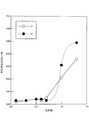
そして、図8は、図6および図7に示す関係から、各試料S1〜S7の光沢度と発光効率Eとの関係を示すグラフ図である。
図8から明らかなように、リードフレームがほぼ無光沢となる光沢度=0.1およびリードフレームがほぼ鏡面光沢となる光沢度=1.3と比較して、リードフレームが半光沢となる光沢度=0.3〜1.0の範囲において、より高い発光効率Eが得られることがわかる。また、特に光沢度=0.5〜0.7の範囲において、より高い発光効率Eが得られることがわかる。これは、例えばリードフレームの光沢度が0.1の場合には、そのときのリードフレームの光吸収率が12%まで増加しているために、リードフレームによる光吸収の影響が大きくなるためである。一方、例えばリードフレームの光沢度が1.3の場合には、リードフレームの反射特性が鏡面反射に近づいているために、リードフレームで反射した光が出射面65cから抜け出るまでの反射回数が増大し、リードフレームや白色樹脂による光吸収の影響が大きくなるためである。したがって、リードフレームの光沢度を0.3〜1.0の範囲、より好ましくは0.5〜0.7の範囲より選択すればよいことが理解される。
FIG. 8 is a graph showing the relationship between the glossiness of each of the samples S1 to S7 and the light emission efficiency E based on the relationships shown in FIGS.
As can be seen from FIG. 8, the gloss of the lead frame becomes semi-gloss as compared to the gloss level of 0.1 where the lead frame is almost non-gloss = 0.1 and the gloss level of 1.3 where the lead frame is almost specular. It can be seen that higher luminous efficiency E is obtained in the range of degree = 0.3 to 1.0. It can also be seen that higher luminous efficiency E can be obtained particularly in the glossiness range of 0.5 to 0.7. This is because, for example, when the glossiness of the lead frame is 0.1, the light absorption rate of the lead frame at that time has increased to 12%, so that the influence of light absorption by the lead frame increases. is there. On the other hand, for example, when the glossiness of the lead frame is 1.3, since the reflection characteristics of the lead frame are close to mirror reflection, the number of reflections until the light reflected by the lead frame escapes from the
また、図9は、図6および図7に示す関係から、各試料S1〜S7の光沢度と、出射面65cに対し垂直な方向におけるx値、y値それぞれの最大最小差xΔmax-minおよびyΔmax-minとの関係を示すグラフ図である。なお、図9では、例えばx値の最大最小差xΔmax-minを、(x)として示し、y値の最大最小差yΔmax-minを(y)として示している。
FIG. 9 shows the glossiness of each of the samples S1 to S7 and the maximum and minimum differences xΔmax-min and yΔmax between the x value and the y value in the direction perpendicular to the
図9より明らかなように、リードフレームがほぼ鏡面光沢となる光沢度=1.3と比較して、光沢度=0.1〜1.0の範囲において、各発光装置60の出射面65c上において、垂直方向のx値、y値のばらつきが小さくなること、換言すれば、各発光装置60から出射される光の色むらが抑制されることがわかる。
As can be seen from FIG. 9, on the
一方、図10は、図6および図7に示す関係から、各試料S1〜S7の光沢度と、出射面65cに対し平行な方向におけるx値、y値それぞれの最大最小差xΔmax-minおよびyΔmax-minとの関係を示すグラフ図である。なお、図10では、図9と同様に、例えばx値の最大最小差xΔmax-minを、(x)として示し、y値の最大最小差yΔmax-minを(y)として示している。
On the other hand, FIG. 10 shows the relationship between the glossiness of each of the samples S1 to S7 and the maximum and minimum differences xΔmax-min and yΔmax between the x value and the y value in the direction parallel to the
図10から明らかなように、リードフレームがほぼ鏡面光沢となる光沢度=1.3と比較して、光沢度=0.1〜1.0の範囲において、各発光装置60の出射面65c上において、平行方向のx値、y値のばらつきが小さくなること、換言すれば、各発光装置60から出射される光の色むらが抑制されることがわかる。ただし、図8に示したように、リードフレームがほぼ無光沢となる光沢度=0.1の場合には、リードフレームが半光沢となる光沢度=0.3〜1.0の場合よりも、発光効率Eが低くなる。したがって、リードフレームの光沢度を0.3〜1.0の範囲、より好ましくは0.5〜0.7の範囲より選択すればよいことが理解される。
As can be seen from FIG. 10, on the
さらに、図11は、図6および図7に示す関係から、各試料S1〜S7の光沢度と、発光装置60間の色度yのばらつきとの関係を示すグラフ図である。なお、ここでは、各試料S1〜S7をそれぞれ20個ずつ用意し、各試料S1〜S7を構成するそれぞれ20個の発光装置60から出力される光の色度yのばらつきを、σで評価している。
Further, FIG. 11 is a graph showing the relationship between the glossiness of each of the samples S1 to S7 and the variation in chromaticity y between the light emitting
図11から明らかなように、リードフレームがほぼ鏡面光沢となる光沢度=1.3と比較して、光沢度=0.1〜1.0の範囲において、より色度yのばらつきσが小さくなること、換言すれば、発光装置60間での色むらが抑制されることがわかる。ただし、図8にも示したように、リードフレームがほぼ無光沢となる光沢度=0.1の場合には、リードフレームが半光沢となる光沢度=0.3〜1.0の場合よりも、発光効率Eが低くなる。したがって、リードフレームの光沢度を0.3〜1.0の範囲、より好ましくは0.5〜0.7の範囲より選択すればよいことが理解される。
As is apparent from FIG. 11, the variation σ of the chromaticity y is smaller in the range of glossiness = 0.1 to 1.0 compared to the glossiness = 1.3 where the lead frame is almost specular. In other words, it can be seen that uneven color between the light emitting
10…バックライト装置、12…発光モジュール、50…液晶表示モジュール、51…液晶パネル、60…発光装置、61…樹脂容器、61a…凹部、61b…上面、62a…第1アノード用リード部、62b…第2アノード用リード部、62c…第3アノード用リード部、63…カソード用リード部、64a…第1半導体発光素子、64b…第2半導体発光素子、64c…第3半導体発光素子、65…封止樹脂、65a…蛍光体粉体、65b…透明樹脂、65c…出射面、70…底面、80…壁面
DESCRIPTION OF
Claims (17)
金属導体と、当該金属導体の表面に形成された0.3以上且つ1.0以下の光沢度を有する銀メッキ層とを有し、前記樹脂容器の前記凹部の前記底面に露出した状態で配置される導体部と、
前記凹部の前記底面において、当該底面の中心位置とは異なる位置に取り付けられ、前記導体部と電気的に接続される発光素子と、
前記発光素子の発光波長に対して透明な透明樹脂と、当該透明樹脂に分散され当該発光素子の発光波長をより長波長の光に変換する蛍光体とを含み、前記凹部において当該発光素子を封止する封止樹脂と
を含む発光装置。 A resin container having a recess including a bottom surface and a wall surface rising from the periphery of the bottom surface;
It has a metal conductor and a silver plating layer having a glossiness of 0.3 or more and 1.0 or less formed on the surface of the metal conductor, and is arranged in a state exposed on the bottom surface of the recess of the resin container A conductor portion to be
A light emitting element attached to a position different from a center position of the bottom surface on the bottom surface of the concave portion and electrically connected to the conductor portion;
A transparent resin transparent to the light emission wavelength of the light emitting element, and a phosphor dispersed in the transparent resin and converting the light emission wavelength of the light emitting element into light having a longer wavelength, and sealing the light emitting element in the recess. A light emitting device including a sealing resin to be stopped.
前記蛍光体は、前記青色光を緑色光に変換して出力する第1の蛍光体と、当該青色光を赤色光に変換して出力する第2の蛍光体とを含むことを特徴とする請求項1ないし4のいずれか1項記載の発光装置。 The light emitting element outputs blue light,
The phosphor includes a first phosphor that converts the blue light into green light and outputs the light, and a second phosphor that converts the blue light into red light and outputs the light. Item 5. The light emitting device according to any one of Items 1 to 4.
前記出射面は、前記樹脂容器との境界部側から中央部側に向けて凹む凹状の形状を有し、当該出射面の凹み量が、20μm以上且つ100μm以下の範囲に設定されることを特徴とする請求項1ないし6のいずれか1項記載の発光装置。 The sealing resin has an emission surface for emitting the light output from the light emitting element to the outside,
The exit surface has a concave shape that is recessed from the boundary side with the resin container toward the center side, and the amount of recess of the exit surface is set in a range of 20 μm or more and 100 μm or less. The light-emitting device according to claim 1.
金属導体と、当該金属導体の表面に形成された0.3以上且つ1.0以下の光沢度を有する銀メッキ層とを有し、前記樹脂容器の前記凹部の内側に露出した状態で形成される導体部と、
前記凹部の内側に設けられ、前記導体部と電気的に接続される複数の発光素子と、
前記複数の発光素子の発光波長に対して透明な透明樹脂と、当該透明樹脂に分散され当該発光素子の発光波長をより長波長の光に変換する蛍光体とを含み、前記凹部において当該複数の発光素子を封止する封止樹脂と
を含む発光装置。 A resin container having a recess;
It has a metal conductor and a silver plating layer having a glossiness of 0.3 or more and 1.0 or less formed on the surface of the metal conductor, and is formed in a state of being exposed inside the recess of the resin container. A conductor portion;
A plurality of light emitting elements provided inside the recess and electrically connected to the conductor portion;
A transparent resin transparent to the emission wavelength of the plurality of light emitting elements, and a phosphor that is dispersed in the transparent resin and converts the emission wavelength of the light emitting element into light having a longer wavelength. A light emitting device including a sealing resin for sealing the light emitting element.
前記基板に取り付けられる複数の発光装置とを備え、
前記発光装置は、
底面と、当該底面の周縁から立ち上がる壁面とを含む凹部を備えた樹脂容器と、
金属導体と、当該金属導体の表面に形成された0.3以上且つ1.0以下の光沢度を有する銀メッキ層とを有し、前記樹脂容器の前記凹部の前記底面に露出した状態で配置される導体部と、
前記凹部の前記底面において、当該底面の中心位置とは異なる位置に取り付けられ、前記導体部と電気的に接続される発光素子と、
前記発光素子の発光波長に対して透明な透明樹脂と、当該透明樹脂に分散され当該発光素子の発光波長をより長波長の光に変換する蛍光体とを含み、前記凹部において当該発光素子を封止する封止樹脂と
を有することを特徴とする発光モジュール。 A substrate,
A plurality of light emitting devices attached to the substrate;
The light emitting device
A resin container having a recess including a bottom surface and a wall surface rising from the periphery of the bottom surface;
It has a metal conductor and a silver plating layer having a glossiness of 0.3 or more and 1.0 or less formed on the surface of the metal conductor, and is arranged in a state exposed on the bottom surface of the recess of the resin container A conductor portion to be
A light emitting element attached to a position different from a center position of the bottom surface on the bottom surface of the concave portion and electrically connected to the conductor portion;
A transparent resin transparent to the light emission wavelength of the light emitting element, and a phosphor dispersed in the transparent resin and converting the light emission wavelength of the light emitting element into light having a longer wavelength, and sealing the light emitting element in the recess. A light emitting module comprising: a sealing resin that stops.
Priority Applications (4)
| Application Number | Priority Date | Filing Date | Title |
|---|---|---|---|
| JP2008233986A JP5220527B2 (en) | 2008-09-11 | 2008-09-11 | Light emitting device, light emitting module |
| PCT/JP2009/065247 WO2010029872A1 (en) | 2008-09-09 | 2009-09-01 | Light emitting unit, light emitting module, and display device |
| US13/062,152 US8378369B2 (en) | 2008-09-09 | 2009-09-01 | Light emitting unit, light emitting module, and display device |
| TW098130222A TWI425655B (en) | 2008-09-09 | 2009-09-08 | A light emitting device, a light emitting module, and a display device |
Applications Claiming Priority (1)
| Application Number | Priority Date | Filing Date | Title |
|---|---|---|---|
| JP2008233986A JP5220527B2 (en) | 2008-09-11 | 2008-09-11 | Light emitting device, light emitting module |
Publications (2)
| Publication Number | Publication Date |
|---|---|
| JP2010067863A true JP2010067863A (en) | 2010-03-25 |
| JP5220527B2 JP5220527B2 (en) | 2013-06-26 |
Family
ID=42193176
Family Applications (1)
| Application Number | Title | Priority Date | Filing Date |
|---|---|---|---|
| JP2008233986A Expired - Fee Related JP5220527B2 (en) | 2008-09-09 | 2008-09-11 | Light emitting device, light emitting module |
Country Status (1)
| Country | Link |
|---|---|
| JP (1) | JP5220527B2 (en) |
Cited By (10)
| Publication number | Priority date | Publication date | Assignee | Title |
|---|---|---|---|---|
| WO2011125428A1 (en) * | 2010-04-01 | 2011-10-13 | 京セラ株式会社 | Light emitting device |
| JP2011222641A (en) * | 2010-04-07 | 2011-11-04 | Nichia Chem Ind Ltd | Light-emitting device |
| KR20110125070A (en) * | 2010-05-12 | 2011-11-18 | 엘지이노텍 주식회사 | Light-emitting element package |
| JP2013084690A (en) * | 2011-10-06 | 2013-05-09 | Sharp Corp | Light-emitting diode package and backlight device |
| JP2013201399A (en) * | 2012-03-26 | 2013-10-03 | Furukawa Electric Co Ltd:The | Substrate of lead frame for optical semiconductor device, lead frame for optical semiconductor device using the same and manufacturing method therefor, and optical semiconductor device |
| US8926114B2 (en) | 2010-04-30 | 2015-01-06 | Samsung Electronics Co., Ltd. | Light emitting device package, light source module, backlight unit, display apparatus, television set, and illumination apparatus |
| JP2015041683A (en) * | 2013-08-21 | 2015-03-02 | 大日本印刷株式会社 | Lead frame with resin, manufacturing method thereof, led package and manufacturing method thereof |
| JP2015050320A (en) * | 2013-09-02 | 2015-03-16 | 株式会社リコー | Optical device and image formation device |
| JP2015073131A (en) * | 2015-01-05 | 2015-04-16 | ローム株式会社 | Led light emitter and led bulb |
| KR101873998B1 (en) * | 2011-07-28 | 2018-07-05 | 엘지이노텍 주식회사 | Light emitting device package and lighting system including the same |
Citations (9)
| Publication number | Priority date | Publication date | Assignee | Title |
|---|---|---|---|---|
| JP2004363537A (en) * | 2002-09-05 | 2004-12-24 | Nichia Chem Ind Ltd | Semiconductor equipment, manufacturing method therefor and optical device using the same |
| JP2005146191A (en) * | 2003-11-19 | 2005-06-09 | Kaneka Corp | Curable resin composition for semiconductor package and semiconductor |
| JP2006228856A (en) * | 2005-02-16 | 2006-08-31 | Ngk Spark Plug Co Ltd | Wiring board for packaging light emitting device |
| JP2006269531A (en) * | 2005-03-22 | 2006-10-05 | Matsushita Electric Ind Co Ltd | Optical semiconductor apparatus |
| JP2007080990A (en) * | 2005-09-13 | 2007-03-29 | Showa Denko Kk | Light emitting device |
| WO2007142018A1 (en) * | 2006-06-02 | 2007-12-13 | Hitachi Chemical Co., Ltd. | Package for mounting optical semiconductor element and optical semiconductor device employing the same |
| JP2008041699A (en) * | 2006-08-01 | 2008-02-21 | Showa Denko Kk | Led package |
| JP2008187188A (en) * | 2004-04-27 | 2008-08-14 | Matsushita Electric Ind Co Ltd | Light emitting device |
| JP2008201828A (en) * | 2007-02-16 | 2008-09-04 | Nippon Steel Chem Co Ltd | Light-emitting diode |
-
2008
- 2008-09-11 JP JP2008233986A patent/JP5220527B2/en not_active Expired - Fee Related
Patent Citations (9)
| Publication number | Priority date | Publication date | Assignee | Title |
|---|---|---|---|---|
| JP2004363537A (en) * | 2002-09-05 | 2004-12-24 | Nichia Chem Ind Ltd | Semiconductor equipment, manufacturing method therefor and optical device using the same |
| JP2005146191A (en) * | 2003-11-19 | 2005-06-09 | Kaneka Corp | Curable resin composition for semiconductor package and semiconductor |
| JP2008187188A (en) * | 2004-04-27 | 2008-08-14 | Matsushita Electric Ind Co Ltd | Light emitting device |
| JP2006228856A (en) * | 2005-02-16 | 2006-08-31 | Ngk Spark Plug Co Ltd | Wiring board for packaging light emitting device |
| JP2006269531A (en) * | 2005-03-22 | 2006-10-05 | Matsushita Electric Ind Co Ltd | Optical semiconductor apparatus |
| JP2007080990A (en) * | 2005-09-13 | 2007-03-29 | Showa Denko Kk | Light emitting device |
| WO2007142018A1 (en) * | 2006-06-02 | 2007-12-13 | Hitachi Chemical Co., Ltd. | Package for mounting optical semiconductor element and optical semiconductor device employing the same |
| JP2008041699A (en) * | 2006-08-01 | 2008-02-21 | Showa Denko Kk | Led package |
| JP2008201828A (en) * | 2007-02-16 | 2008-09-04 | Nippon Steel Chem Co Ltd | Light-emitting diode |
Cited By (11)
| Publication number | Priority date | Publication date | Assignee | Title |
|---|---|---|---|---|
| WO2011125428A1 (en) * | 2010-04-01 | 2011-10-13 | 京セラ株式会社 | Light emitting device |
| JP2011222641A (en) * | 2010-04-07 | 2011-11-04 | Nichia Chem Ind Ltd | Light-emitting device |
| US8926114B2 (en) | 2010-04-30 | 2015-01-06 | Samsung Electronics Co., Ltd. | Light emitting device package, light source module, backlight unit, display apparatus, television set, and illumination apparatus |
| KR20110125070A (en) * | 2010-05-12 | 2011-11-18 | 엘지이노텍 주식회사 | Light-emitting element package |
| KR101659355B1 (en) | 2010-05-12 | 2016-09-23 | 엘지이노텍 주식회사 | Light-emitting element package |
| KR101873998B1 (en) * | 2011-07-28 | 2018-07-05 | 엘지이노텍 주식회사 | Light emitting device package and lighting system including the same |
| JP2013084690A (en) * | 2011-10-06 | 2013-05-09 | Sharp Corp | Light-emitting diode package and backlight device |
| JP2013201399A (en) * | 2012-03-26 | 2013-10-03 | Furukawa Electric Co Ltd:The | Substrate of lead frame for optical semiconductor device, lead frame for optical semiconductor device using the same and manufacturing method therefor, and optical semiconductor device |
| JP2015041683A (en) * | 2013-08-21 | 2015-03-02 | 大日本印刷株式会社 | Lead frame with resin, manufacturing method thereof, led package and manufacturing method thereof |
| JP2015050320A (en) * | 2013-09-02 | 2015-03-16 | 株式会社リコー | Optical device and image formation device |
| JP2015073131A (en) * | 2015-01-05 | 2015-04-16 | ローム株式会社 | Led light emitter and led bulb |
Also Published As
| Publication number | Publication date |
|---|---|
| JP5220527B2 (en) | 2013-06-26 |
Similar Documents
| Publication | Publication Date | Title |
|---|---|---|
| WO2010029872A1 (en) | Light emitting unit, light emitting module, and display device | |
| JP5220527B2 (en) | Light emitting device, light emitting module | |
| JP5220526B2 (en) | Light emitting device, light emitting module, display device | |
| JP7096512B2 (en) | Luminescent device | |
| JPWO2005091387A1 (en) | Light emitting device and lighting device | |
| CN102299246A (en) | Light-Emitting Device | |
| JP2006253336A (en) | Light source device | |
| JP5220522B2 (en) | Light emitting device, light emitting module | |
| JP6524624B2 (en) | Light emitting device | |
| JP2007088060A (en) | Light emitting device | |
| US20230207752A1 (en) | Light-emitting device and method of manufacturing the same | |
| JP2007173408A (en) | Light-emitting device | |
| KR20120045539A (en) | Light emitting device package | |
| US10454007B2 (en) | Light-emitting device and method for manufacturing same | |
| JP2007173733A (en) | Light emitting device | |
| KR20030031061A (en) | Light emitting device having highly efficient color conversion layer and method for manufacturing thereof | |
| JP2014195046A (en) | Light emitting device and lighting device including the same | |
| US9190580B2 (en) | Phosphor and light emitting device having the same | |
| US10336936B2 (en) | Phosphor and light emitting device having the same | |
| JP2010199629A (en) | Semiconductor light emitting device | |
| JP2007288125A (en) | Light emitting device | |
| JP2007234817A (en) | Light-emitting device | |
| KR20170073353A (en) | Light emitting device and lighting system having thereof | |
| WO2016035508A1 (en) | Light emitting device | |
| KR20170073360A (en) | Phosphor, light emitting device having thereof and light unit having thereof |
Legal Events
| Date | Code | Title | Description |
|---|---|---|---|
| A621 | Written request for application examination |
Free format text: JAPANESE INTERMEDIATE CODE: A621 Effective date: 20110601 |
|
| A131 | Notification of reasons for refusal |
Free format text: JAPANESE INTERMEDIATE CODE: A131 Effective date: 20120403 |
|
| A02 | Decision of refusal |
Free format text: JAPANESE INTERMEDIATE CODE: A02 Effective date: 20120918 |
|
| A521 | Written amendment |
Free format text: JAPANESE INTERMEDIATE CODE: A523 Effective date: 20121212 |
|
| A911 | Transfer to examiner for re-examination before appeal (zenchi) |
Free format text: JAPANESE INTERMEDIATE CODE: A911 Effective date: 20121219 |
|
| TRDD | Decision of grant or rejection written | ||
| A01 | Written decision to grant a patent or to grant a registration (utility model) |
Free format text: JAPANESE INTERMEDIATE CODE: A01 Effective date: 20130219 |
|
| A61 | First payment of annual fees (during grant procedure) |
Free format text: JAPANESE INTERMEDIATE CODE: A61 Effective date: 20130306 |
|
| FPAY | Renewal fee payment (event date is renewal date of database) |
Free format text: PAYMENT UNTIL: 20160315 Year of fee payment: 3 |
|
| R150 | Certificate of patent or registration of utility model |
Free format text: JAPANESE INTERMEDIATE CODE: R150 |
|
| LAPS | Cancellation because of no payment of annual fees |