JP2010060341A - 磁気センサ - Google Patents
磁気センサ Download PDFInfo
- Publication number
- JP2010060341A JP2010060341A JP2008224297A JP2008224297A JP2010060341A JP 2010060341 A JP2010060341 A JP 2010060341A JP 2008224297 A JP2008224297 A JP 2008224297A JP 2008224297 A JP2008224297 A JP 2008224297A JP 2010060341 A JP2010060341 A JP 2010060341A
- Authority
- JP
- Japan
- Prior art keywords
- magnetic
- magnetoresistive element
- magnetosensitive
- electrode
- magnetoresistive
- Prior art date
- Legal status (The legal status is an assumption and is not a legal conclusion. Google has not performed a legal analysis and makes no representation as to the accuracy of the status listed.)
- Granted
Links
- 239000000758 substrate Substances 0.000 claims abstract description 37
- 239000004020 conductor Substances 0.000 claims abstract description 13
- 238000001514 detection method Methods 0.000 claims description 55
- 230000035945 sensitivity Effects 0.000 claims description 19
- 230000004907 flux Effects 0.000 claims description 12
- 238000003491 array Methods 0.000 claims description 2
- 239000004065 semiconductor Substances 0.000 abstract description 14
- 230000015572 biosynthetic process Effects 0.000 description 18
- 238000010586 diagram Methods 0.000 description 11
- 230000001681 protective effect Effects 0.000 description 10
- WPYVAWXEWQSOGY-UHFFFAOYSA-N indium antimonide Chemical compound [Sb]#[In] WPYVAWXEWQSOGY-UHFFFAOYSA-N 0.000 description 2
- 239000000463 material Substances 0.000 description 2
- 229910001218 Gallium arsenide Inorganic materials 0.000 description 1
- 229910004298 SiO 2 Inorganic materials 0.000 description 1
- 230000000694 effects Effects 0.000 description 1
- 239000000696 magnetic material Substances 0.000 description 1
- 230000035807 sensation Effects 0.000 description 1
Images

Classifications
-
- G—PHYSICS
- G01—MEASURING; TESTING
- G01R—MEASURING ELECTRIC VARIABLES; MEASURING MAGNETIC VARIABLES
- G01R33/00—Arrangements or instruments for measuring magnetic variables
- G01R33/02—Measuring direction or magnitude of magnetic fields or magnetic flux
- G01R33/06—Measuring direction or magnitude of magnetic fields or magnetic flux using galvano-magnetic devices
- G01R33/09—Magnetoresistive devices
- G01R33/093—Magnetoresistive devices using multilayer structures, e.g. giant magnetoresistance sensors
-
- B—PERFORMING OPERATIONS; TRANSPORTING
- B82—NANOTECHNOLOGY
- B82Y—SPECIFIC USES OR APPLICATIONS OF NANOSTRUCTURES; MEASUREMENT OR ANALYSIS OF NANOSTRUCTURES; MANUFACTURE OR TREATMENT OF NANOSTRUCTURES
- B82Y25/00—Nanomagnetism, e.g. magnetoimpedance, anisotropic magnetoresistance, giant magnetoresistance or tunneling magnetoresistance
-
- G—PHYSICS
- G01—MEASURING; TESTING
- G01R—MEASURING ELECTRIC VARIABLES; MEASURING MAGNETIC VARIABLES
- G01R33/00—Arrangements or instruments for measuring magnetic variables
- G01R33/0005—Geometrical arrangement of magnetic sensor elements; Apparatus combining different magnetic sensor types
-
- G—PHYSICS
- G01—MEASURING; TESTING
- G01R—MEASURING ELECTRIC VARIABLES; MEASURING MAGNETIC VARIABLES
- G01R33/00—Arrangements or instruments for measuring magnetic variables
- G01R33/02—Measuring direction or magnitude of magnetic fields or magnetic flux
- G01R33/06—Measuring direction or magnitude of magnetic fields or magnetic flux using galvano-magnetic devices
Landscapes
- Physics & Mathematics (AREA)
- Condensed Matter Physics & Semiconductors (AREA)
- General Physics & Mathematics (AREA)
- Chemical & Material Sciences (AREA)
- Engineering & Computer Science (AREA)
- Nanotechnology (AREA)
- Crystallography & Structural Chemistry (AREA)
- Measuring Magnetic Variables (AREA)
- Hall/Mr Elements (AREA)
Abstract
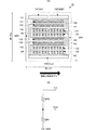
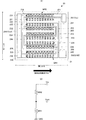
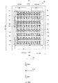
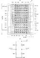
【解決手段】基板11上には、磁気抵抗素子MR1を構成する感磁部121〜124と、磁気抵抗素子MR2を構成する感磁部131〜134とが形成されている。感磁部121〜124,131〜134は長尺状の半導体膜により形成されており、さらに感磁部121〜124の半導体膜上には導電性材料からなる短絡電極が長尺方向に沿って所定間隔で形成されている。感磁部121〜124,131〜134は、それぞれの長尺方向が平行に並び且つ近接するように形成される。この際、感磁部121〜124,131〜134は、磁気抵抗素子MR2の感磁部131,132、磁気抵抗素子MR1の感磁部121,122、磁気抵抗素子MR2の感磁部133,134、磁気抵抗素子MR1の感磁部123,124の順に配列されるように、形成される。
【選択図】図1
Description
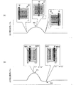
基板41における磁気検出部40の形成領域の第一方向(図5(A)における縦方向)に沿った一方端には、電圧入力用電極491、グランド接続用電極492が形成されており、他方端には、電圧出力用電極493が形成されている。
基板51における磁気検出部50の形成領域の第二方向(図6(A)における横方向)に沿った一方端には、電圧入力用電極5911,5912、グランド接続用電極5921,5922が形成されており、他方端には、電圧出力用電極5931,5932が形成されている。
Claims (6)
- 通過磁束により抵抗値の変化する感磁部を基板表面に形成してなる複数の磁気抵抗素子を直列接続し、該直列接続された複数の磁気抵抗素子によって分圧される電圧を出力信号とする磁気検出部を備えた磁気センサであって、
前記磁気抵抗素子のそれぞれは、長尺状に形成された複数の前記感磁部と、該複数の前記感磁部を直列接続する接続導体部と、を有し、
前記複数の磁気抵抗素子をそれぞれ構成する複数の感磁部は、一方向に並んで配置され、
一つの磁気抵抗素子を構成する少なくとも一つの感磁部が当該一つの磁気抵抗素子を構成する他の複数の感磁部に対して両側から隣り合わないように、全ての磁気抵抗素子の感磁部が配置されている、磁気センサ。 - 前記複数の磁気抵抗素子は異なる感度を有し、
前記一つの磁気抵抗素子の一つの感磁部と、前記一つの磁気抵抗素子と感度の異なる別の磁気抵抗素子の一つの感磁部とが隣り合うように配置された一対の配列が複数形成されている、請求項1に記載の磁気センサ。 - 前記複数の磁気抵抗素子をそれぞれ構成する複数の感磁部は、前記長尺方向に垂直な方向に沿って平行になるように配置されている、請求項1または請求項2に記載の磁気センサ。
- 前記長尺方向が被検出体の搬送方向に平行である、請求項1〜請求項3のいずれかに記載の磁気センサ。
- 前記感磁部を接続する接続電極は、前記基板の前記感磁部を有する面とともに、当該面に対して前記感磁部を覆うように形成された絶縁層の表面にも形成されている、請求項1〜請求項4のいずれかに記載の磁気センサ。
- 前記磁気検出部を複数備え、該複数の磁気検出部に対して、前記一つの磁気抵抗素子を構成する一つの感磁部が当該一つの磁気抵抗素子を構成する他の複数の感磁部に対して両側から隣り合わないように、全ての磁気抵抗素子の感磁部を配置する、請求項1〜請求項5のいずれかに記載の磁気センサ。
Priority Applications (4)
| Application Number | Priority Date | Filing Date | Title |
|---|---|---|---|
| JP2008224297A JP4735686B2 (ja) | 2008-09-02 | 2008-09-02 | 磁気センサ |
| EP09251952A EP2159586B1 (en) | 2008-09-02 | 2009-08-06 | Magnetic sensor |
| KR1020090081261A KR20100027979A (ko) | 2008-09-02 | 2009-08-31 | 자기 센서 |
| CN200910170660.3A CN101666864B (zh) | 2008-09-02 | 2009-09-01 | 磁性传感器 |
Applications Claiming Priority (1)
| Application Number | Priority Date | Filing Date | Title |
|---|---|---|---|
| JP2008224297A JP4735686B2 (ja) | 2008-09-02 | 2008-09-02 | 磁気センサ |
Related Child Applications (1)
| Application Number | Title | Priority Date | Filing Date |
|---|---|---|---|
| JP2011025890A Division JP4771015B2 (ja) | 2011-02-09 | 2011-02-09 | 磁気センサ |
Publications (2)
| Publication Number | Publication Date |
|---|---|
| JP2010060341A true JP2010060341A (ja) | 2010-03-18 |
| JP4735686B2 JP4735686B2 (ja) | 2011-07-27 |
Family
ID=41278876
Family Applications (1)
| Application Number | Title | Priority Date | Filing Date |
|---|---|---|---|
| JP2008224297A Expired - Fee Related JP4735686B2 (ja) | 2008-09-02 | 2008-09-02 | 磁気センサ |
Country Status (4)
| Country | Link |
|---|---|
| EP (1) | EP2159586B1 (ja) |
| JP (1) | JP4735686B2 (ja) |
| KR (1) | KR20100027979A (ja) |
| CN (1) | CN101666864B (ja) |
Cited By (2)
| Publication number | Priority date | Publication date | Assignee | Title |
|---|---|---|---|---|
| CN103267955A (zh) * | 2013-05-28 | 2013-08-28 | 江苏多维科技有限公司 | 单芯片桥式磁场传感器 |
| CN110998349A (zh) * | 2017-08-16 | 2020-04-10 | 株式会社村田制作所 | 磁传感器 |
Families Citing this family (8)
| Publication number | Priority date | Publication date | Assignee | Title |
|---|---|---|---|---|
| US7220602B2 (en) * | 2005-07-29 | 2007-05-22 | Freescale Semiconductor, Inc. | Magnetic tunnel junction sensor method |
| CN102683582A (zh) * | 2011-03-11 | 2012-09-19 | 曲炳郡 | 一种高灵敏度磁传感芯片的制造方法 |
| JP5867235B2 (ja) | 2011-05-16 | 2016-02-24 | 三菱電機株式会社 | 磁気センサ装置 |
| TWI409488B (zh) * | 2011-09-29 | 2013-09-21 | Voltafield Technology Corp | 磁阻感測元件與磁阻感測裝置 |
| CN103090888A (zh) * | 2011-11-04 | 2013-05-08 | 新科实业有限公司 | 带有旁路层的磁传感器及其制造方法 |
| WO2018116783A1 (ja) * | 2016-12-21 | 2018-06-28 | 株式会社村田製作所 | 磁気センサ |
| WO2018204356A1 (en) * | 2017-05-01 | 2018-11-08 | The Board Of Trustees Of The Leland Stanford Junior University | Methods for accurate temperature measurement on gmr biosensor arrays |
| CN110535456B (zh) * | 2019-08-26 | 2024-07-26 | 基康仪器股份有限公司 | 一种基于磁敏的编码控制方法及开关系统 |
Citations (8)
| Publication number | Priority date | Publication date | Assignee | Title |
|---|---|---|---|---|
| JPS5011588A (ja) * | 1973-05-31 | 1975-02-06 | ||
| JPS59114412A (ja) * | 1982-12-21 | 1984-07-02 | Copal Co Ltd | 磁気抵抗素子を具える磁気検出器 |
| JPH01300578A (ja) * | 1988-05-30 | 1989-12-05 | Fujitsu Ltd | 磁気抵抗素子 |
| JPH08313296A (ja) * | 1995-05-23 | 1996-11-29 | Sankyo Seiki Mfg Co Ltd | 磁気検出装置 |
| JP2001004728A (ja) * | 1999-09-02 | 2001-01-12 | Micro Magune Kk | 磁気検出装置 |
| JP2003188438A (ja) * | 2001-12-18 | 2003-07-04 | Murata Mfg Co Ltd | 磁気抵抗素子 |
| JP2003215222A (ja) * | 2002-01-23 | 2003-07-30 | Denso Corp | 磁気抵抗効果素子センサ |
| JP2006098088A (ja) * | 2004-09-28 | 2006-04-13 | Yamaha Corp | 巨大磁気抵抗効果素子を用いた磁気センサ及び同磁気センサの製造方法 |
Family Cites Families (1)
| Publication number | Priority date | Publication date | Assignee | Title |
|---|---|---|---|---|
| TWI278650B (en) * | 2004-09-28 | 2007-04-11 | Yamaha Corp | Magnetic sensor using giant magnetoresistive elements and method for manufacturing the same |
-
2008
- 2008-09-02 JP JP2008224297A patent/JP4735686B2/ja not_active Expired - Fee Related
-
2009
- 2009-08-06 EP EP09251952A patent/EP2159586B1/en not_active Not-in-force
- 2009-08-31 KR KR1020090081261A patent/KR20100027979A/ko not_active Ceased
- 2009-09-01 CN CN200910170660.3A patent/CN101666864B/zh not_active Expired - Fee Related
Patent Citations (8)
| Publication number | Priority date | Publication date | Assignee | Title |
|---|---|---|---|---|
| JPS5011588A (ja) * | 1973-05-31 | 1975-02-06 | ||
| JPS59114412A (ja) * | 1982-12-21 | 1984-07-02 | Copal Co Ltd | 磁気抵抗素子を具える磁気検出器 |
| JPH01300578A (ja) * | 1988-05-30 | 1989-12-05 | Fujitsu Ltd | 磁気抵抗素子 |
| JPH08313296A (ja) * | 1995-05-23 | 1996-11-29 | Sankyo Seiki Mfg Co Ltd | 磁気検出装置 |
| JP2001004728A (ja) * | 1999-09-02 | 2001-01-12 | Micro Magune Kk | 磁気検出装置 |
| JP2003188438A (ja) * | 2001-12-18 | 2003-07-04 | Murata Mfg Co Ltd | 磁気抵抗素子 |
| JP2003215222A (ja) * | 2002-01-23 | 2003-07-30 | Denso Corp | 磁気抵抗効果素子センサ |
| JP2006098088A (ja) * | 2004-09-28 | 2006-04-13 | Yamaha Corp | 巨大磁気抵抗効果素子を用いた磁気センサ及び同磁気センサの製造方法 |
Cited By (4)
| Publication number | Priority date | Publication date | Assignee | Title |
|---|---|---|---|---|
| CN103267955A (zh) * | 2013-05-28 | 2013-08-28 | 江苏多维科技有限公司 | 单芯片桥式磁场传感器 |
| JP2016524142A (ja) * | 2013-05-28 | 2016-08-12 | 江▲蘇▼多▲維▼科技有限公司Multidimension Technology Co., Ltd. | シングルチップ・ブリッジ型磁場センサ |
| CN110998349A (zh) * | 2017-08-16 | 2020-04-10 | 株式会社村田制作所 | 磁传感器 |
| CN110998349B (zh) * | 2017-08-16 | 2021-11-16 | 株式会社村田制作所 | 磁传感器 |
Also Published As
| Publication number | Publication date |
|---|---|
| EP2159586B1 (en) | 2013-02-13 |
| EP2159586A3 (en) | 2010-10-13 |
| EP2159586A2 (en) | 2010-03-03 |
| CN101666864B (zh) | 2016-02-03 |
| KR20100027979A (ko) | 2010-03-11 |
| JP4735686B2 (ja) | 2011-07-27 |
| CN101666864A (zh) | 2010-03-10 |
Similar Documents
| Publication | Publication Date | Title |
|---|---|---|
| JP4735686B2 (ja) | 磁気センサ | |
| KR101429356B1 (ko) | 3개의 접점을 갖는 홀 효과 영역을 포함하는 전자 디바이스 | |
| US20100123458A1 (en) | Twin vertical hall sensor | |
| US12032042B2 (en) | Current sensor for compensation of on-die temperature gradient | |
| JP5888402B2 (ja) | 磁気センサ素子 | |
| CN100420953C (zh) | 磁阻传感器 | |
| CN107533113B (zh) | 具有增加的snr的磁场传感器 | |
| US10101414B2 (en) | Thin film resistive device for use in an integrated circuit, an integrated circuit including a thin film resistive device | |
| JP4798191B2 (ja) | 磁気センサ装置 | |
| US11243275B2 (en) | Magnetic field sensing device | |
| JP7020176B2 (ja) | 磁気センサ | |
| JP2018535391A (ja) | 磁気イメージセンサー | |
| JP6267613B2 (ja) | 磁気センサおよびその磁気センサを備えた電流センサ | |
| JP5413866B2 (ja) | 磁気検出素子を備えた電流センサ | |
| JP4771015B2 (ja) | 磁気センサ | |
| US8957680B2 (en) | Magnetic sensor and pattern for magnetic sensor | |
| JP4345813B2 (ja) | 長尺型磁気センサ | |
| JP2023046271A (ja) | 磁気センサ | |
| KR20230089608A (ko) | 3축 자기저항 센서 | |
| JP4914502B2 (ja) | 磁気センサ及び磁気エンコーダ | |
| EP4386408A1 (en) | Magnetic sensor device for sensing a magnetic field and having low sensitivity to inhomogeneities in the magnetic field | |
| US20260023137A1 (en) | Magnetic sensor and manufacturing method for the same | |
| JP7119351B2 (ja) | 磁気センサ | |
| JP2008060454A (ja) | 磁気デバイス | |
| JP2010133854A (ja) | 磁気検出回路素子および磁気センサ |
Legal Events
| Date | Code | Title | Description |
|---|---|---|---|
| A621 | Written request for application examination |
Free format text: JAPANESE INTERMEDIATE CODE: A621 Effective date: 20100201 |
|
| A131 | Notification of reasons for refusal |
Free format text: JAPANESE INTERMEDIATE CODE: A131 Effective date: 20100413 |
|
| A521 | Request for written amendment filed |
Free format text: JAPANESE INTERMEDIATE CODE: A523 Effective date: 20100614 |
|
| RD02 | Notification of acceptance of power of attorney |
Free format text: JAPANESE INTERMEDIATE CODE: A7422 Effective date: 20100614 |
|
| A131 | Notification of reasons for refusal |
Free format text: JAPANESE INTERMEDIATE CODE: A131 Effective date: 20100817 |
|
| A521 | Request for written amendment filed |
Free format text: JAPANESE INTERMEDIATE CODE: A523 Effective date: 20101018 |
|
| A02 | Decision of refusal |
Free format text: JAPANESE INTERMEDIATE CODE: A02 Effective date: 20101109 |
|
| A521 | Request for written amendment filed |
Free format text: JAPANESE INTERMEDIATE CODE: A523 Effective date: 20110209 |
|
| A911 | Transfer to examiner for re-examination before appeal (zenchi) |
Free format text: JAPANESE INTERMEDIATE CODE: A911 Effective date: 20110217 |
|
| TRDD | Decision of grant or rejection written | ||
| A01 | Written decision to grant a patent or to grant a registration (utility model) |
Free format text: JAPANESE INTERMEDIATE CODE: A01 Effective date: 20110329 |
|
| A61 | First payment of annual fees (during grant procedure) |
Free format text: JAPANESE INTERMEDIATE CODE: A61 Effective date: 20110411 |
|
| R150 | Certificate of patent or registration of utility model |
Ref document number: 4735686 Country of ref document: JP Free format text: JAPANESE INTERMEDIATE CODE: R150 Free format text: JAPANESE INTERMEDIATE CODE: R150 |
|
| FPAY | Renewal fee payment (event date is renewal date of database) |
Free format text: PAYMENT UNTIL: 20140513 Year of fee payment: 3 |
|
| LAPS | Cancellation because of no payment of annual fees |