JP2010060341A - Magnetic sensor - Google Patents
Magnetic sensor Download PDFInfo
- Publication number
- JP2010060341A JP2010060341A JP2008224297A JP2008224297A JP2010060341A JP 2010060341 A JP2010060341 A JP 2010060341A JP 2008224297 A JP2008224297 A JP 2008224297A JP 2008224297 A JP2008224297 A JP 2008224297A JP 2010060341 A JP2010060341 A JP 2010060341A
- Authority
- JP
- Japan
- Prior art keywords
- magnetic
- magnetoresistive element
- magnetosensitive
- electrode
- magnetoresistive
- Prior art date
- Legal status (The legal status is an assumption and is not a legal conclusion. Google has not performed a legal analysis and makes no representation as to the accuracy of the status listed.)
- Granted
Links
Images

Classifications
-
- G—PHYSICS
- G01—MEASURING; TESTING
- G01R—MEASURING ELECTRIC VARIABLES; MEASURING MAGNETIC VARIABLES
- G01R33/00—Arrangements or instruments for measuring magnetic variables
- G01R33/02—Measuring direction or magnitude of magnetic fields or magnetic flux
- G01R33/06—Measuring direction or magnitude of magnetic fields or magnetic flux using galvano-magnetic devices
- G01R33/09—Magnetoresistive devices
- G01R33/093—Magnetoresistive devices using multilayer structures, e.g. giant magnetoresistance sensors
-
- B—PERFORMING OPERATIONS; TRANSPORTING
- B82—NANOTECHNOLOGY
- B82Y—SPECIFIC USES OR APPLICATIONS OF NANOSTRUCTURES; MEASUREMENT OR ANALYSIS OF NANOSTRUCTURES; MANUFACTURE OR TREATMENT OF NANOSTRUCTURES
- B82Y25/00—Nanomagnetism, e.g. magnetoimpedance, anisotropic magnetoresistance, giant magnetoresistance or tunneling magnetoresistance
-
- G—PHYSICS
- G01—MEASURING; TESTING
- G01R—MEASURING ELECTRIC VARIABLES; MEASURING MAGNETIC VARIABLES
- G01R33/00—Arrangements or instruments for measuring magnetic variables
- G01R33/0005—Geometrical arrangement of magnetic sensor elements; Apparatus combining different magnetic sensor types
-
- G—PHYSICS
- G01—MEASURING; TESTING
- G01R—MEASURING ELECTRIC VARIABLES; MEASURING MAGNETIC VARIABLES
- G01R33/00—Arrangements or instruments for measuring magnetic variables
- G01R33/02—Measuring direction or magnitude of magnetic fields or magnetic flux
- G01R33/06—Measuring direction or magnitude of magnetic fields or magnetic flux using galvano-magnetic devices
Abstract
Description
この発明は、被検出体に備えられた磁気パターン等の磁気情報を検出する磁気センサに関するものである。 The present invention relates to a magnetic sensor for detecting magnetic information such as a magnetic pattern provided on a detection object.
従来、紙幣等の被検出体に組み込まれた磁気パターンや磁気情報を検出する磁気センサが各種考案されている。 2. Description of the Related Art Conventionally, various magnetic sensors for detecting a magnetic pattern and magnetic information incorporated in a detection object such as a bill have been devised.
例えば、特許文献1には、基板上にミアンダ形状の磁気抵抗効果膜が形成されてなる一般的な差動型の磁気センサが示されている。また、特許文献2にも、磁気抵抗素子を複数備えた差動型の磁気センサが示されている。ここで、より具体的に特許文献2の図24に示すように、各磁気抵抗素子は、長尺状からなる複数の感磁部を有し、該複数の感磁部は被検出体の検知範囲において一方向に並んで配置されるとともに直列接続されている。 For example, Patent Document 1 discloses a general differential type magnetic sensor in which a meander-shaped magnetoresistive film is formed on a substrate. Patent Document 2 also shows a differential magnetic sensor including a plurality of magnetoresistive elements. More specifically, as shown in FIG. 24 of Patent Document 2, each magnetoresistive element has a plurality of long magnetic sensing portions, and the plurality of magnetic sensing portions are detected by a detection target. They are arranged side by side in one direction and connected in series.
そして、このように磁気抵抗素子を直列接続して分圧した電圧を出力すること、すなわち差分出力することで、磁気抵抗素子の有する温度により抵抗値が変化する抵抗温度特性の影響を抑制している。
しかしながら、上述のような従来の磁気センサでは、差分出力に利用する複数の磁気抵抗素子の形成位置が離間している。ここで、磁気センサは、例えば、当該磁気センサが搭載される機器内に設置されており、当該機器内の熱源で発生する熱等が磁気センサ全体に均一に伝達されるとは限らない。このため、各磁気抵抗素子の形成位置で温度が異なってしまい、上述のような抵抗温度特性による影響の抑制効果が得られなくなる。その結果、温度が異なることにより、複数の磁気抵抗素子間で抵抗値の変化が大きくなり、差分出力が変動してしまう。 However, in the conventional magnetic sensor as described above, the formation positions of a plurality of magnetoresistive elements used for differential output are separated. Here, the magnetic sensor is installed in, for example, a device on which the magnetic sensor is mounted, and heat generated by a heat source in the device is not necessarily transmitted uniformly to the entire magnetic sensor. For this reason, the temperature differs depending on the formation position of each magnetoresistive element, and the effect of suppressing the influence due to the resistance temperature characteristic as described above cannot be obtained. As a result, when the temperatures are different, the resistance value changes greatly between the plurality of magnetoresistive elements, and the differential output fluctuates.
したがって、本発明の目的は、複数の磁気抵抗素子の温度を均一にできる構造の磁気センサを実現することにある。 Therefore, an object of the present invention is to realize a magnetic sensor having a structure capable of making the temperatures of a plurality of magnetoresistive elements uniform.
この発明は、通過磁束により抵抗値の変化する感磁部を基板表面に形成してなる複数の磁気抵抗素子を直列接続し、該直列接続された複数の磁気抵抗素子によって分圧される電圧を出力信号とする磁気検出部を備えた磁気センサに関するものである。そして、この磁気センサの各磁気抵抗素子は、それぞれが長尺状に形成された複数の感磁部と、該複数の感磁部を直列接続する接続導体部と、を有する。さらに、複数の磁気抵抗素子をそれぞれ構成する複数の感磁部は、一方向に並んで配置され、一つの磁気抵抗素子を構成する少なくとも一つの感磁部が当該一つの磁気抵抗素子を構成する他の複数の感磁部に対して両側から隣り合わないように、全ての磁気抵抗素子の感磁部が配置される。 In the present invention, a plurality of magnetoresistive elements formed by forming a magnetosensitive part whose resistance value is changed by a passing magnetic flux on a substrate surface are connected in series, and a voltage divided by the plurality of magnetoresistive elements connected in series is obtained. The present invention relates to a magnetic sensor including a magnetic detection unit as an output signal. Each magnetoresistive element of the magnetic sensor has a plurality of magnetic sensing portions each formed in a long shape, and a connection conductor portion connecting the plurality of magnetic sensing portions in series. Further, the plurality of magnetosensitive parts constituting each of the plurality of magnetoresistive elements are arranged in one direction, and at least one magnetosensitive part constituting one magnetoresistive element constitutes the one magnetoresistive element. The magnetic sensitive parts of all the magnetoresistive elements are arranged so as not to be adjacent to the other magnetic sensitive parts from both sides.
この構成では、全ての磁気抵抗素子に対して、単体の磁気抵抗素子を構成する全ての感磁部が一箇所に集合して形成されない。例えば、第1磁気抵抗素子と第2磁気抵抗素子とからなる二つの磁気抵抗素子がそれぞれ第1感磁部、第2感磁部の二つを有する場合、第1磁気抵抗素子の第1感磁部、第2磁気抵抗素子の第1感磁部、第1磁気抵抗素子の第2感磁部、第2磁気抵抗素子の第2感磁部の順に並んで形成される。このため、従来のように各磁気抵抗素子をそれぞれ構成する感磁部群が異なる領域にそれぞれ設置される場合と比較して、各磁気抵抗素子の感磁部で感温される温度の差が低減される。 In this configuration, all the magnetosensitive parts constituting the single magnetoresistive element are not collectively formed at one place with respect to all the magnetoresistive elements. For example, when two magnetoresistive elements including a first magnetoresistive element and a second magnetoresistive element have two first and second magnetosensitive parts, respectively, the first sensation of the first magnetoresistive element. The magnetic part, the first magnetosensitive part of the second magnetoresistive element, the second magnetosensitive part of the first magnetoresistive element, and the second magnetosensitive part of the second magnetoresistive element are arranged in this order. For this reason, compared with the case where the magnetosensitive part group which comprises each magnetoresistive element each is installed in a different area | region conventionally, the difference of the temperature sensed by the magnetosensitive part of each magnetoresistive element is different. Reduced.
また、この発明の磁気センサは、複数の磁気抵抗素子が異なる感度を有し、一つの磁気抵抗素子の一つの感磁部と、一つの磁気抵抗素子と感度の異なる別の磁気抵抗素子の一つの感磁部とが隣り合うように配置された一対の配列が複数形成されている。 In the magnetic sensor of the present invention, a plurality of magnetoresistive elements have different sensitivities, one magnetosensitive part of one magnetoresistive element, and one magnetoresistive element having a different sensitivity from one magnetoresistive element. A plurality of pairs of arrays are formed so that two magnetic sensing portions are adjacent to each other.
この構成では、異なる感度からなる複数の磁気抵抗素子を構成する感磁部同士が、隣り合うことで一つの感磁部対として構成される。そして、これら異なる感度の感磁部の組からなる感磁部対が順次配列される構成になることで、それぞれに異なる磁気抵抗素子を構成する感度の異なる各感磁部群間での温度差がより一層低減される。 In this configuration, the magnetosensitive parts constituting a plurality of magnetoresistive elements having different sensitivities are adjacent to each other so as to be configured as one magnetosensitive part pair. Then, by arranging the magnetic sensing part pairs composed of the magnetic sensing parts having different sensitivities in sequence, the temperature difference between the magnetic sensitive parts having different sensitivities constituting the respective magnetoresistive elements. Is further reduced.
また、この発明の磁気センサは、複数の磁気抵抗素子をそれぞれ構成する複数の感磁部が長尺方向に垂直な方向に沿って平行になるように配置されている。 In the magnetic sensor of the present invention, the plurality of magnetic sensing parts respectively constituting the plurality of magnetoresistive elements are arranged in parallel along a direction perpendicular to the longitudinal direction.
この構成では、隣り合う感磁部同士での最も離れた部分間の距離が、長尺方向に沿って並ぶ場合よりも短くなる。すなわち、長尺方向に並ぶ場合では感磁部の長尺方向の長さの約2倍であるのに対して、長尺方向に垂直な方向に並ぶ場合では感磁部の短い幅の約2倍でしかない。このような構成とすることで、異なる磁気抵抗素子の隣り合う感磁部同士での感温は略同じとなる。これにより、複数の磁気抵抗素子の温度が略均一になる。 In this configuration, the distance between the farthest portions between the adjacent magnetic sensing portions is shorter than that in the case where they are arranged along the longitudinal direction. That is, in the case of being arranged in the longitudinal direction, it is about twice the length in the longitudinal direction of the magnetic sensing part, whereas in the case of being arranged in the direction perpendicular to the longitudinal direction, it is about 2 of the short width of the magnetic sensing part. It is only double. By setting it as such a structure, the temperature sensitivity in the adjacent magnetosensitive part of a different magnetoresistive element becomes substantially the same. Thereby, the temperature of a some magnetoresistive element becomes substantially uniform.
また、この発明の磁気センサは、長尺方向が被検出体の搬送方向に平行である。 In the magnetic sensor of the present invention, the longitudinal direction is parallel to the conveyance direction of the detection target.
この構成では、各磁気抵抗素子での被検出体からの磁気検出タイミングが一致する。このため、例えば、磁気抵抗素子間で感度が異なるように設定されていれば、感度が低い側の磁気抵抗素子の出力が、感度の高い側の磁気抵抗素子の出力に打ち消され、単純な波形の出力が得られる。この際、各磁気抵抗素子の抵抗温度特性は異ならず、温度も同じであるので、抵抗温度特性の影響を抑圧することができる。 In this configuration, the magnetic detection timing from the detection object in each magnetoresistive element matches. For this reason, for example, if the sensitivity is set to be different between the magnetoresistive elements, the output of the magnetoresistive element on the low sensitivity side is canceled by the output of the magnetoresistive element on the high sensitivity side, and a simple waveform is obtained. Is obtained. At this time, the resistance temperature characteristics of the magnetoresistive elements are not different and the temperature is the same, so that the influence of the resistance temperature characteristics can be suppressed.
また、この発明の磁気センサは、感磁部を接続する接続電極が、基板の感磁部を有する面とともに、当該面に対して感磁部を覆うように形成された絶縁層の表面にも形成されている。 In addition, the magnetic sensor of the present invention has a connection electrode for connecting the magnetic sensitive part on the surface of the insulating layer formed to cover the magnetic sensitive part with respect to the surface of the substrate having the magnetic sensitive part. Is formed.
この構成では、感磁部が形成された基板の表面に、全ての接続電極を形成しなくても良いので、基板表面での感磁部の密集率を向上させることができる。これにより、複数の磁気抵抗素子の温度をより均一にできる。また、感磁部や接続電極の引き回しが容易になる。 In this configuration, since it is not necessary to form all the connection electrodes on the surface of the substrate on which the magnetic sensitive portion is formed, the density of the magnetic sensitive portions on the substrate surface can be improved. Thereby, the temperature of a some magnetoresistive element can be made more uniform. Further, the magnetic sensing part and the connection electrode can be easily routed.
また、この発明の磁気センサは、磁気検出部を複数備え、該複数の磁気検出部に対して、一つの磁気抵抗素子を構成する一つの感磁部が当該一つの磁気抵抗素子を構成する他の複数の感磁部に対して両側から隣り合わないように、全ての磁気抵抗素子の感磁部を配置している。 In addition, the magnetic sensor of the present invention includes a plurality of magnetic detection units, and one magnetosensitive unit constituting one magnetoresistive element constitutes the one magnetoresistive element with respect to the plurality of magnetic detection units. The magnetosensitive parts of all the magnetoresistive elements are arranged so as not to be adjacent to the plurality of magnetosensitive parts from both sides.
この構成では、複数の磁気検出部を構成する各磁気抵抗素子の感磁部が、磁気抵抗素子毎に集中せず、上述のように各磁気抵抗素子の感磁部が配列方向に沿って交代しながら順に配置される。これにより、複数の磁気検出部を有する構成であっても、各磁気検出部を構成する磁気抵抗素子の感磁部の温度が均一になる。 In this configuration, the magnetosensitive elements of the magnetoresistive elements constituting the plurality of magnetic detectors are not concentrated for each magnetoresistive element, and as described above, the magnetosensitive elements of the magnetoresistive elements alternate along the arrangement direction. Are arranged in order. Thereby, even if it is the structure which has a some magnetic detection part, the temperature of the magnetic sensing part of the magnetoresistive element which comprises each magnetic detection part becomes uniform.
この発明によれば、磁気センサを構成する複数の磁気抵抗素子の温度を均一にすることができるので、磁気抵抗素子が有する抵抗温度特性の影響を抑制することができる。これにより、抵抗温度特性による出力信号の変化を補正する必要が無く、高精度な磁気検知を実現することができる。 According to this invention, since the temperature of the several magnetoresistive element which comprises a magnetic sensor can be made uniform, the influence of the resistance temperature characteristic which a magnetoresistive element has can be suppressed. Thereby, it is not necessary to correct the change of the output signal due to the resistance temperature characteristic, and highly accurate magnetic detection can be realized.
本発明の第1の実施形態に係る磁気センサについて図を参照して説明する。 A magnetic sensor according to a first embodiment of the present invention will be described with reference to the drawings.
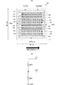
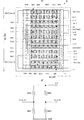
図1(A)は本実施形態の磁気センサの磁気検出部10の構成を示す平面図であり、図1(B)は磁気検出部10の等価回路図である。
FIG. 1A is a plan view showing the configuration of the
磁気検出部10は、図1(A)に示すように、感磁部と、該感磁部を接続する接続ライン電極と、電圧入出力やグランドへの接続に用いる外部接続用電極とを、基板11上に形成することで、図1(B)に示すような回路を構成する。すなわち、磁気抵抗素子MR1,MR2が電圧入力端子Vinとグランド端子GNDとの間に直列接続され、磁気抵抗素子MR1,MR2の接続点に電圧出力端子Voutが接続される回路を構成する。以下に、具体的な構成について示す。
As shown in FIG. 1A, the
基板11は、例えばSi基板からなり、当該Si基板の表面に上述の回路を構成する感磁部(半導体膜)や電極が形成される。なお、基板としては、Si基板等の絶縁性基板の他に、GaAs:SiO2等の半絶縁性基板を用いることができる。基板11における磁気検出部10の形成領域の第一方向(図1(A)における縦方向)に沿った一方端には、電圧入力端子Vinに対応する電圧入力用電極191、グランド端子GNDに対応するグランド接続用電極192が形成されており、他方端には、電圧出力端子Voutに対応する電圧出力用電極193が形成されている。これら電圧入力用電極191、グランド接続用電極192、および電圧出力用電極193は導電性材料からなる。また、電圧入力用電極191、グランド接続用電極192、および電圧出力用電極193は、形成領域の第一方向に垂直な第二方向(図1(A)における横方向)に延びる形状からなる。
The
基板11における電圧入力用電極191およびグランド接続用電極192と、電圧出力用電極193との間の領域には、磁気抵抗素子MR1を構成する感磁部121〜124および接続ライン電極141〜145と、磁気抵抗素子MR2を構成する感磁部131〜134および接続ライン電極151〜155とが形成されている。
In a region between the
磁気抵抗素子MR1の感磁部121〜124は、例えば、InSbを材質とする半導体膜により形成され、長さが幅よりも大きい長尺状のパターンからなる。感磁部121〜124は、長尺方向に沿って、半導体膜上に所定間隔で導電体からなる短絡電極が形成されており、これら短絡電極の形成パターンにより磁界に対する感度が設定されている。ここで磁界に対する感度とは、感磁部を通過する磁束密度に応じて変化する抵抗値を意味し、磁束密度が所定量変化する場合に抵抗値が大きく変化するほど、高感度であると定義される。
The
感磁部121〜124は、長尺方向が前記第二方向に平行になるように配置されている。感磁部121と感磁部122は第一方向において近接して配置され、感磁部123と感磁部124も第一方向において近接して配置される。また、第一方向において、感磁部121,122が平行して形成された領域と、電圧入力用電極191およびグランド接続用電極192が形成された領域との間は、磁気抵抗素子MR2を構成する感磁部131,132が形成可能な距離だけ離間されている。さらに、第一方向において、感磁部121,122が平行して形成された領域と感磁部123,124が平行して形成された領域との間は、磁気抵抗素子MR2を構成する感磁部133,134が形成可能な距離だけ離間されている。そして、感磁部123,124が平行して形成された領域は、電圧出力用電極193に近接している。
The magnetic
磁気抵抗素子MR1の接続ライン電極141〜145は、電圧入力用電極191、グランド接続用電極192および電圧出力用電極193と同じ導電性材料により基板11表面に形成されており、例えば、電圧入力用電極191、グランド接続用電極192および電圧出力用電極193と同時にパターン形成されている。
The connection line electrodes 141 to 145 of the magnetoresistive element MR1 are formed on the surface of the
接続ライン電極141は、互いに離間されたグランド接続用電極192と感磁部121とを電気的に接続するパターンからなり、接続ライン電極142は、互いに近接する感磁部121と感磁部122とを電気的に接続するパターンからなる。接続ライン電極143は、互いに離間された感磁部122と感磁部123とを電気的に接続するパターンからなり、接続ライン電極144は、互いに近接する感磁部123と感磁部124とを電気的に接続するパターンからなる。さらに、接続ライン電極145は、互いに近接する感磁部124と電圧出力用電極193とを接続するパターンからなる。これら接続ライン電極141〜145は、感磁部121〜124の長尺方向の両端に存在する領域に形成されている。
The connection line electrode 141 has a pattern for electrically connecting the
磁気抵抗素子MR2の感磁部131〜134は、例えば、InSbを材質とする半導体膜からなり、長さが幅よりも大きい長尺状のパターンである。感磁部131〜134は、半導体膜上に短絡電極が形成されていない。これにより、感磁部131〜134は、感磁部121〜124よりも磁束に対して低感度に設定されている。
The magnetic
感磁部131〜134は、長尺方向が前記第二方向に平行になるように配置されている。感磁部131と感磁部132は第一方向において近接して配置され、感磁部133と感磁部134も第一方向において近接して配置される。
The magnetic
感磁部131,132は、第一方向において、上述の電圧入力用電極191およびグランド接続用電極192が形成された領域と磁気抵抗素子MR1の感磁部121,122が形成された領域との間に、配置されている。この際、磁気抵抗素子MR2の感磁部131,132と磁気抵抗素子MR1の感磁部121〜124は長尺方向が平行となるように配置される。さらに、磁気抵抗素子MR2の感磁部132と磁気抵抗素子MR1の感磁部121とは、第1方向において近接して配置される。
In the first direction, the magnetic
感磁部133,134は、第一方向において、上述の磁気抵抗素子MR1の感磁部121,122が形成された領域と磁気抵抗素子MR1の感磁部123,124が形成された領域との間に配置されている。この際、磁気抵抗素子MR2の感磁部133,134と磁気抵抗素子MR1の感磁部121〜124は、長尺方向が平行となるように配置される。さらに、磁気抵抗素子MR2の感磁部133と磁気抵抗素子MR1の感磁部122は、第1方向において近接して配置されるとともに、磁気抵抗素子MR2の感磁部134と磁気抵抗素子MR1の感磁部123も、第1方向において近接して配置される。
In the first direction, the magnetic
接続ライン電極151は、互いに近接する電圧入力用電極191と感磁部131とを電気的に接続するパターンからなり、接続ライン電極152は、互いに近接する感磁部131と感磁部132とを電気的に接続するパターンからなる。接続ライン電極153は、互いに離間された感磁部132と感磁部133とを電気的に接続するパターンからなり、接続ライン電極154は、互いに近接する感磁部133と感磁部134とを電気的に接続するパターンからなる。さらに、接続ライン電極155は、互いに離間された感磁部134と電圧出力用電極193とを接続するパターンからなる。これら接続ライン電極151〜155は、感磁部131〜134の長尺方向の両端に存在する領域に形成されている。
The
以上のように、本実施形態の構成では、基板11上の磁気センサ10の形成領域において、第一方向に沿って、一方端(図1(A)の上端)から順に、(i)電圧入力用電極191およびグランド接続用電極192の電極群、(ii)磁気抵抗素子MR2の感磁部131,132、(iii)磁気抵抗素子MR1の感磁部121,122、(iv)磁気抵抗素子MR2の感磁部133,134、(v)磁気抵抗素子MR1の感磁部123,124、(vi)電圧出力用電極193が互いに近接して形成された構造となる。これは、すなわち、磁気抵抗素子MR1の感磁部の形成領域と、磁気抵抗素子MR2の感磁部の形成領域とが、第一方向に沿って、交互に配置されるとともに、これらが近接して配置されていることを意味する。これにより、磁気抵抗素子MR1の形成領域と磁気抵抗素子MR2の形成領域とが集中して離間されないので、磁気抵抗素子MR1の温度と磁気抵抗素子MR2の温度とが略同等になる。特に、本実施形態のように、磁気抵抗素子MR1の感磁部と磁気抵抗素子MR2の感磁部とが交互に複数回繰り返されて配置されることで、単に磁気抵抗素子MR1の感磁部と磁気抵抗素子MR2の感磁部とが隣接して配置されるよりも、さらに温度を同等にすることができる。そして、このような構成とすることで、図1(B)に示すような差動型の出力電圧信号を得る場合に、磁気抵抗素子MR1と磁気抵抗素子MR2との間での温度差を無くすことができるので、磁気抵抗素子MR1,MR2の抵抗温度特性に影響されることなく、磁気抵抗素子MR1,MR2の感磁量に応じた正確な出力電圧信号を得ることができる。
As described above, in the configuration of the present embodiment, in the formation region of the
さらに、上述の第二方向を被検出体の搬送方向とすることで、磁気抵抗素子MR1,MR2を構成する感磁部121〜124、131〜134の配列方向が、被検出体の搬送方向に直交する。これにより、被検出体による通過磁束の変化に応じた磁気抵抗素子MR1の抵抗値変化と磁気抵抗素子MR2の抵抗値変化とが時間軸上で一致する。ここで、上述のように、磁気抵抗素子MR2の感度を磁気抵抗素子MR1の感度よりも低くすることで、磁気抵抗素子MR2の抵抗値変化が、磁気抵抗素子MR1の抵抗値変化により打ち消される。
Furthermore, by setting the above-mentioned second direction as the transport direction of the detected object, the arrangement direction of the magnetic
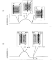
図2は本実施形態の構成の磁気センサの磁気検出部10と従来の構成(上述の特許文献2の図24の構成)の磁気センサの磁気検出部との出力電圧信号の波形を説明するための図であり、図2(A)が本実施形態の磁気センサの磁気検出部10の場合を示し、図2(B)が従来の構成の磁気センサの磁気検出部の場合を示す。
FIG. 2 is a diagram for explaining waveforms of output voltage signals from the
図2(A)に示すように、本実施形態の構成を用いることで、出力電圧信号は、被検出体Mの通過に伴い発生するピーク(P0)が一つのみの波形となり、被検出体Mを正確に検知することができる。この際、上述のように磁気抵抗素子MR1,MR2の温度(T°)が一致するので、抵抗温度特性の影響を相殺でき、被検出体Mの磁束密度の大きさに応じた正確な出力電圧信号レベルが得られる。一方で、図2(B)に示すように、従来の構成を用いると、出力電圧信号は被検出体Mが磁気抵抗素子MR1を通過した際のピーク(P1)と、被検出体が磁気抵抗素子MR2を通過した際のピーク(P2)との二つのピークを有することになる。このため、一つの被検出体に対して二つのピークが検知されることになってしまう。そして、これらのピークは、それぞれの磁気抵抗素子MR1,MR2の形成位置の温度に依存するので、これら形成位置の温度が相違すれば、これらを単に加減算や乗除算しても、抵抗温度特性の影響を相殺することができず、被検出体の磁束密度の大きさに応じた出力電圧信号レベルを正確に検知することができない。 As shown in FIG. 2 (A), by using the configuration of the present embodiment, the output voltage signal has a waveform with only one peak (P0) generated along the passage of the detected object M, and the detected object. M can be detected accurately. At this time, since the temperatures (T °) of the magnetoresistive elements MR1 and MR2 coincide with each other as described above, the influence of the resistance temperature characteristics can be offset, and an accurate output voltage corresponding to the magnitude of the magnetic flux density of the detection target M can be obtained. A signal level is obtained. On the other hand, as shown in FIG. 2B, when the conventional configuration is used, the output voltage signal has a peak (P1) when the detected object M passes the magnetoresistive element MR1, and the detected object is magnetoresistive. It has two peaks, a peak (P2) when passing through the element MR2. For this reason, two peaks will be detected with respect to one to-be-detected body. Since these peaks depend on the temperatures of the formation positions of the magnetoresistive elements MR1 and MR2, if the temperatures of these formation positions are different, even if they are simply added or subtracted or multiplied and divided, The influence cannot be canceled out, and the output voltage signal level corresponding to the magnitude of the magnetic flux density of the detected object cannot be detected accurately.
次に、第2の実施形態に係る磁気センサについて図を参照して説明する。 Next, a magnetic sensor according to a second embodiment will be described with reference to the drawings.
図3(A)は本実施形態の磁気センサの磁気検出部20の構成を示す平面図であり、図3(B)は磁気センサの磁気検出部20の等価回路図である。
FIG. 3A is a plan view showing the configuration of the
本実施形態に示す磁気検出部20も、第1の実施形態に示した磁気検出部10と同様に、基板21上に感磁部や導電性の電極を形成することで、図3(B)に示す回路を構成する。そして、基板21、感磁部、導電性の電極の材質も第1の実施形態と同じである。
Similarly to the
基板21における磁気検出部20の形成領域の第二方向(図3(A)における横方向)に沿った一方端には、電圧入力用電極291、グランド接続用電極292が形成されており、他方端には、電圧出力用電極293が形成されている。
A
基板21における電圧入力用電極291およびグランド接続用電極292と、電圧出力用電極293との間の領域には、磁気抵抗素子MR1を構成する感磁部221〜225および接続ライン電極241〜246と、磁気抵抗素子MR2を構成する感磁部231〜235および接続ライン電極251〜256とが形成されている。
In the region between the
磁気抵抗素子MR1の感磁部221〜225は、長さが幅よりも大きい長尺状のパターンであり、長尺方向に沿って、半導体膜上に所定間隔で導電体からなる短絡電極が形成されている。感磁部221〜225は、長尺方向が前記第二方向に平行になるように配置されている。
The
感磁部221と感磁部222は第一方向において近接して配置され、感磁部222と感磁部223は第一方向において磁気抵抗素子MR2の感磁部232,233が形成可能な距離だけ離間されている。感磁部223と感磁部224は第一方向において近接して配置され、感磁部224と感磁部225は第一方向において磁気抵抗素子MR2の感磁部234,235が形成可能な距離だけ離間されている。
The magnetic
感磁部221とグランド接続用電極292は、接続ライン電極241により電気的に接続され、感磁部221,222は接続ライン電極242により電気的に接続される。感磁部222,223は接続ライン電極243により電気的に接続され、感磁部223、224は接続ライン電極244により電気的に接続される。感磁部224,225は接続ライン電極245により電気的に接続され、感磁部225と電圧出力用電極293は接続ライン電極246により電気的に接続される。
The magnetic
磁気抵抗素子MR2の感磁部231〜235は、長さが幅よりも大きい長尺状のパターンであり、短絡電極が形成されていない。感磁部231〜235は、感磁部221〜225と同様に、長尺方向が前記第二方向に平行になるように配置されている。
The
感磁部231は、磁気抵抗素子MR1の感磁部221に対して感磁部222と対向する側で、感磁部221に近接して配置されている。
The
感磁部232と感磁部233は第一方向において近接するように、上述の磁気抵抗素子MR1の感磁部222と感磁部223との間の領域に配置されている。感磁部234と感磁部235は第一方向において近接するように、上述の磁気抵抗素子MR1の感磁部224と感磁部225との間の領域に配置されている。
The
感磁部231と電圧入力用電極291は、接続ライン電極251によりに電気的に接続され、感磁部231,232は接続ライン電極252により電気的に接続される。感磁部232,233は接続ライン電極253により電気的に接続され、感磁部233、234は接続ライン電極254により電気的に接続される。感磁部234,235は接続ライン電極255により電気的に接続され、感磁部235と電圧出力用電極293は接続ライン電極256により電気的に接続される。
The
このような構成とすることで、二つの磁気抵抗素子MR1の感磁部221〜225と磁気抵抗素子MR2の感磁部231〜235は、第一方向に沿って、感磁部231、感磁部221、感磁部222、感磁部232、感磁部233、感磁部223、感磁部224、感磁部234、感磁部235、感磁部225の順に配列される。
With this configuration, the
ここで、本実施形態では、構成する磁気抵抗素子が異なる組み合わせからなる隣り合う感磁部間の距離、例えば感磁部231と感磁部221との距離が、構成する磁気抵抗素子が同じ組み合わせからなる隣り合う感磁部間の距離、例えば感磁部221と感磁部222との距離よりも、さらに短く設定されている。
Here, in the present embodiment, the distance between adjacent magnetic sensing parts composed of different combinations of the magnetoresistive elements, for example, the distance between the magnetic
このような構成により、磁気抵抗素子MR2の感磁部231と磁気抵抗素子MR1の感磁部221と組み合わせのように、異なる磁気抵抗素子を構成する感磁部同士が極近接された位置に配置される。これにより、第1の実施形態よりも、さらに磁気抵抗素子MR1,MR2間での温度差が無くなり、抵抗温度特性の影響をより効果的に抑制した出力電圧信号を得ることができる。
With such a configuration, the magnetic sensitive parts constituting the different magnetoresistive elements are arranged in close proximity to each other like the magnetic
また、本実施形態においても感磁部の配列方向を被検出体搬送方向に直交させることで、被検出体の検知を正確に行うことができる。 Also in this embodiment, the detection object can be detected accurately by making the arrangement direction of the magnetic sensing parts orthogonal to the detection object conveyance direction.
次に、第3の実施形態に係る磁気センサについて図を参照して説明する。 Next, a magnetic sensor according to a third embodiment will be described with reference to the drawings.
図4(A)は本実施形態の磁気センサの磁気検出部30の構成を示す平面図であり、図4(B)は磁気センサの磁気検出部30の等価回路図である。
FIG. 4A is a plan view showing the configuration of the
本実施形態の磁気センサの磁気検出部30は、上述の第1、第2の実施形態に示したような出力電圧信号が一つ得られる構成ではなく、一つの電圧入力に対して、二つの出力電圧信号が得られる構成である。すなわち、図4(B)に示すように等価回路としては、電圧入力端子Vinとグランド端子(GND)との間に、磁気抵抗素子MR3,MR1の直列回路と、磁気抵抗素子MR2,MR4の直列回路とが並列接続され、磁気抵抗素子MR3,MR1の接続点が電圧出力端子Vout−Aに接続され、磁気抵抗素子MR2,MR4の接続点が電圧出力端子Vout−Bに接続される。
The
また、本実施形態に示す磁気検出部30も、第1、第2の実施形態に示した磁気検出部10,20と同様に、基板31上に感磁部や導電性の電極を形成することで、図4(B)に示す回路を構成する。そして、基板31、感磁部、導電性の電極の材質も第1、第2の実施形態と同じである。
The
基板31における磁気検出部30の形成領域の第二方向(図4(A)における横方向)に沿った一方端には、電圧入力端子Vinに対応する二つの電圧入力用電極3911,3912と、電圧出力端子Vout−Aに対応する一つ電圧出力用電極3931が形成されており、他方端には、グランド端子GNDに対応する二つのグランド接続用電極3921,3922と、電圧出力端子Vout−Bに対応する一つ電圧出力用電極3932が形成されている。
Two
基板31における第二方向の一方端と他方端との間の領域には、磁気抵抗素子MR1を構成する感磁部3211,3221,3231および接続ライン電極3411,3421,3431,3441と、磁気抵抗素子MR2を構成する感磁部3312,3322,3332および接続ライン電極3512,3522,3532,3542と、磁気抵抗素子MR3を構成する感磁部3311,3321および接続ライン電極3511,3521,3441と、磁気抵抗素子MR4を構成する感磁部3212,3222および接続ライン電極3412,3422,3542とが形成されている。ここで、電圧出力用電極3931に接続する接続ライン電極3441は磁気抵抗素子MR1,MR3で共通であり、電圧出力用電極3932に接続する接続ライン電極3542は磁気抵抗素子MR2,MR4で共通である。
In a region between one end and the other end of the
磁気抵抗素子MR1を構成する感磁部3211,3221,3231は、長さが幅よりも大きい長尺状のパターンであり、長尺方向に沿って、半導体膜上に所定間隔で導電体からなる短絡電極が形成されている。感磁部3211,3221,3231は、長尺方向が前記第二方向に平行になるように配置されている。
The magnetic
感磁部3211と感磁部3221は、第一方向において、磁気抵抗素子MR2の感磁部3332、3322、磁気抵抗素子MR4の感磁部3222,3212が形成可能な距離だけ離間されている。感磁部3221と感磁部3231は、第一方向において磁気抵抗素子MR3の感磁部3311,3321が形成可能な距離だけ離間されている。
In the first direction, the
感磁部3211とグランド接続用電極3921は接続ライン電極3411により電気的に接続され、感磁部3211,3221は接続ライン電極3421により電気的に接続され、感磁部3221,3231は接続ライン電極3431により電気的に接続され、感磁部3231と電圧出力用電極3931は接続ライン電極3441により電気的に接続されている。
The
磁気抵抗素子MR2を構成する感磁部3312,3322,3332は、長さが幅よりも大きい長尺状のパターンであり、長尺方向に沿って、半導体膜上に所定間隔で導電体からなる短絡電極が形成されている。感磁部3312,3322,3332は、長尺方向が前記第二方向に平行になるように配置されている。
The magnetic
感磁部3332は、磁気抵抗素子MR1の感磁部3211,3221間における、磁気抵抗素子MR1の感磁部3211に近接して設置されている。感磁部3322は、磁気抵抗素子MR1の感磁部3211,3221間における、磁気抵抗素子MR1の感磁部3221に近接して設置されている。この際、磁気抵抗素子MR2の感磁部3332,3322は、第一方向において磁気抵抗素子MR4の感磁部3212,3222が形成可能な距離だけ離間されている。
The
感磁部3312は、第一方向において磁気抵抗素子MR1の感磁部3231に対して感磁部3221,3322と反対側で且つ感磁部3231に近接して配置されている。
The
感磁部3312と電圧入力用電極3912は接続ライン電極3512により電気的に接続され、感磁部3312,3322は接続ライン電極3522により電気的に接続され、感磁部3322,3332は接続ライン電極3532により電気的に接続され、感磁部3332と電圧出力用電極3932は、接続ライン電極3542により電気的に接続されている。
The
磁気抵抗素子MR3を構成する感磁部3311,3321は、長さが幅よりも大きい長尺状のパターンであり、半導体膜上に導電体からなる短絡電極は形成されていない。感磁部3311,3321は、長尺方向が前記第二方向に平行になるように配置されている。
The magnetic
感磁部3311,3321は、第一方向における磁気抵抗素子MR1の感磁部3221,3231間に、近接するように配置されている。
The magnetic
感磁部3311と電圧入力用電極3911は接続ライン電極3511により電気的に接続され、感磁部3311,3321は接続ライン電極3521により電気的に接続され、感磁部3321と電圧出力用電極3931は、接続ライン電極3441により電気的に接続されている。
The
磁気抵抗素子MR4を構成する感磁部3212,3222は、長さが幅よりも大きい長尺状のパターンであり、半導体膜上に導電体からなる短絡電極は形成されていない。感磁部3212,3222は、長尺方向が前記第二方向に平行になるように配置されている。
The magnetic
感磁部3212,3222は、第一方向における磁気抵抗素子MR2の感磁部3332,3322間に、近接するように配置されている。
The magnetic
感磁部3212とグランド接続用電極3922は接続ライン電極3412により電気的に接続され、感磁部3212,3222は接続ライン電極3422により電気的に接続され、感磁部3222と電圧出力用電極3932は、接続ライン電極3542により電気的に接続されている。
The magnetic sensing part 3212 and the
このような構成とすることで、基板31上の第一方向に沿って、磁気抵抗素子MR1の感磁部3211、磁気抵抗素子MR2の感磁部3332、磁気抵抗素子MR4の感磁部3222,3212、磁気抵抗素子MR2の感磁部3322、磁気抵抗素子MR1の感磁部3221、磁気抵抗素子MR3の感磁部3311,3321、磁気抵抗素子MR1の感磁部3231、磁気抵抗素子MR2の感磁部3312が順に近接して配置される。
With such a configuration, along the first direction on the
これにより、磁気抵抗素子MR1〜MR4の感磁部は、磁気抵抗素子MR1〜MR4毎に集中せず、入り組んだ構成となる。この結果、一つの入力電圧で二つの出力電圧が得られる磁気センサであっても、上述の各実施形態のように、磁気抵抗素子MR1〜MR4の抵抗温度特性による影響を抑制することができる。 As a result, the magnetosensitive portions of the magnetoresistive elements MR1 to MR4 are not concentrated for each of the magnetoresistive elements MR1 to MR4, and are intricately configured. As a result, even a magnetic sensor that can obtain two output voltages with one input voltage can suppress the influence of the resistance temperature characteristics of the magnetoresistive elements MR1 to MR4 as in the above-described embodiments.
なお、このような磁束変化に対する応答が時間軸上で一致する二つの出力電圧信号が得られることを利用し、これら二つの出力電圧信号の一方を極性反転処理して、二つの出力電圧信号を加算することで、よりピークレベルが高く、ピークが一つとなる検出信号を得ることができる。これにより、磁束密度の差に応じた検出信号のレベル差も大きくなるので、磁束密度に対する検出分解能を向上させることができ、より高精度な磁気センサを実現することができる。 By utilizing the fact that two output voltage signals whose responses to magnetic flux changes coincide on the time axis are obtained, one of these two output voltage signals is subjected to polarity inversion processing, and the two output voltage signals are By adding, a detection signal having a higher peak level and one peak can be obtained. Thereby, since the level difference of the detection signal according to the difference in magnetic flux density is also increased, the detection resolution with respect to the magnetic flux density can be improved, and a more accurate magnetic sensor can be realized.
次に、第4の実施形態に係る磁気センサについて図を参照して説明する。 Next, a magnetic sensor according to a fourth embodiment will be described with reference to the drawings.
図5(A)は本実施形態の磁気センサの磁気検出部40の構成を示す平面図であり、図5(B)は磁気センサの磁気検出部40の等価回路図である。
FIG. 5A is a plan view showing the configuration of the
上述の各実施形態の磁気センサの磁気検出部では接続ライン電極の全てを基板の表面に直接形成した例を示したが、本実施形態の磁気センサの磁気検出部40は、接続ライン電極の一部が感磁部等の上面に形成された保護膜42の表面に形成されているものである。
In the magnetic detection unit of the magnetic sensor of each embodiment described above, an example in which all of the connection line electrodes are formed directly on the surface of the substrate is shown. However, the
具体的には、磁気検出部40は以下の構成からなる。
基板41における磁気検出部40の形成領域の第一方向(図5(A)における縦方向)に沿った一方端には、電圧入力用電極491、グランド接続用電極492が形成されており、他方端には、電圧出力用電極493が形成されている。
Specifically, the
A
基板41における電圧入力用電極491およびグランド接続用電極492と、電圧出力用電極493との間の領域には、磁気抵抗素子MR1を構成する感磁部421〜424と、磁気抵抗素子MR2を構成する感磁部431〜434とが形成されている。
In a region between the
磁気抵抗素子MR1の感磁部421〜424は、長さが幅よりも大きい長尺状のパターンであり、長尺方向に沿って、半導体膜上に所定間隔で導電体からなる短絡電極が形成されている。感磁部421〜424は、長尺方向が前記第二方向に平行になるように配置されている。
The
磁気抵抗素子MR2の感磁部431〜434は、長さが幅よりも大きい長尺状のパターンであり、短絡電極が形成されていない。感磁部431〜434は、感磁部421〜424と同様に、長尺方向が前記第二方向に平行になるように配置されている。
The
そして、これら感磁部421〜424,431〜434は、第一方向に沿って、構成する磁気抵抗素子が順に交代するように、近接して配置されている。すなわち、電圧入力用電極491、グランド接続用電極492の形成領域側から順に、磁気抵抗素子MR2の感磁部431、磁気抵抗素子MR1の感磁部421、磁気抵抗素子MR2の感磁部432、磁気抵抗素子MR1の感磁部422、磁気抵抗素子MR2の感磁部433、磁気抵抗素子MR1の感磁部423、磁気抵抗素子MR2の感磁部434、磁気抵抗素子MR1の感磁部424が配置されている。
And these magnetic sensitive parts 421-424,431-434 are arrange | positioned adjacently so that the magnetoresistive element to comprise may change in order along a 1st direction. That is, in order from the formation region side of the
また、基板41上には、接続ライン電極441,442,443,445,451,455が形成されている。接続ライン電極441はグランド接続用電極492と感磁部421とを電気的に接続し、接続ライン電極442は感磁部421,422を電気的に接続し、接続ライン電極443は感磁部422,423を電気的に接続し、接続ライン電極445は感磁部424と電圧出力用電極493とを電気的に接続する。接続ライン電極451は電圧入力用電極491と感磁部431とを電気的に接続し、接続ライン電極455は感磁部434と電圧出力用電極493とを電気的に接続する。
In addition,
このような感磁部群と接続ライン電極群との表面には、絶縁性を有する保護膜42が形成されている。保護膜42の表面には、接続ライン電極452,453,454,444が形成されている。接続ライン電極452は保護膜42に形成された図示しないビアホールを介して感磁部431,432を電気的に接続し、接続ライン電極453は保護膜42に形成された図示しないビアホールを介して感磁部432,433を電気的に接続し、接続ライン電極454は保護膜42に形成された図示しないビアホールを介して感磁部433,434を電気的に接続する。また、接続ライン電極444は保護膜42に形成された図示しないビアホールを介して感磁部423,424を電気的に接続する。
A
このような構成とすることで、異なる磁気抵抗素子MR1,MR2をそれぞれに構成する複数の感磁部が、一本毎に第一方向に沿って順次交代しながら配置される。これにより、磁気抵抗素子MR1,MR2での温度を、さらに正確に一致させることができる。 By adopting such a configuration, a plurality of magnetosensitive portions that respectively configure different magnetoresistive elements MR1 and MR2 are arranged alternately one by one along the first direction. As a result, the temperatures at the magnetoresistive elements MR1 and MR2 can be matched more accurately.
また、接続ライン電極を二層に分けて配置することで、電極の引き回しパターンを容易にすることができる。 Further, by arranging the connection line electrodes in two layers, the electrode routing pattern can be facilitated.
次に、第5の実施形態に係る磁気センサについて図を参照して説明する。 Next, a magnetic sensor according to a fifth embodiment will be described with reference to the drawings.
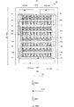
図6(A)は本実施形態の磁気センサの磁気検出部50の構成を示す平面図であり、図5(B)は磁気センサの磁気検出部50の等価回路図である。 FIG. 6A is a plan view showing the configuration of the magnetic detection unit 50 of the magnetic sensor of this embodiment, and FIG. 5B is an equivalent circuit diagram of the magnetic detection unit 50 of the magnetic sensor.
本実施形態の磁気センサの磁気検出部50は、第3の実施形態で示したような一入力二出力の磁気センサに対して、第4の実施形態で示した接続ライン電極の二層構造を適用したものである。 The magnetic detection unit 50 of the magnetic sensor according to the present embodiment has the two-layer structure of the connection line electrodes shown in the fourth embodiment as compared with the one-input two-output magnetic sensor as shown in the third embodiment. It is applied.
具体的には、磁気検出部50は以下の構成からなる。
基板51における磁気検出部50の形成領域の第二方向(図6(A)における横方向)に沿った一方端には、電圧入力用電極5911,5912、グランド接続用電極5921,5922が形成されており、他方端には、電圧出力用電極5931,5932が形成されている。
Specifically, the magnetic detection unit 50 has the following configuration.
また、基板51には、磁気抵抗素子MR1を構成する感磁部5211,5221,5231と、磁気抵抗素子MR2を構成する感磁部5312,5322,5332と、磁気抵抗素子MR3を構成する感磁部5311,5321,5331と、磁気抵抗素子MR4を構成する感磁部5212,5222,5232とが形成されている。
Further, on the
磁気抵抗素子MR1,MR2の感磁部5211,5221,5231、5312,5322,5332は、長さが幅よりも大きい長尺状のパターンであり、短絡電極が形成されておらず、長尺方向が前記第二方向に平行になるように配置されている。
The
磁気抵抗素子MR3,MR4の感磁部5311,5321,5331,5212,5222,5232は、長さが幅よりも大きい長尺状のパターンであり、長尺方向に沿って半導体膜上に所定間隔で導電体からなる短絡電極が形成されており、長尺方向が前記第二方向に平行になるように配置されている。
The magnetic
そして、これらの感磁部は、第一方向に沿って、構成する磁気抵抗素子が順に一本ずつ交代するように、近接して配置されている。すなわち、磁気検出部50の形成領域における第一方向の一方端(図6(A)の上端)から順に、磁気抵抗素子MR4の感磁部5232、磁気抵抗素子MR3の感磁部5311、磁気抵抗素子MR2の感磁部5332、磁気抵抗素子MR1の感磁部5211、磁気抵抗素子MR4の感磁部5222、磁気抵抗素子MR3の感磁部5231、磁気抵抗素子MR2の感磁部5322、磁気抵抗素子MR1の感磁部5221、磁気抵抗素子MR4の感磁部5212、磁気抵抗素子MR3の感磁部5331、磁気抵抗素子MR2の感磁部5312、磁気抵抗素子MR1の感磁部5231が配置されている。
These magnetic sensitive portions are arranged close to each other so that the magnetoresistive elements constituting the magnetic material change one by one along the first direction. That is, in order from the one end in the first direction (the upper end of FIG. 6A) in the formation region of the magnetic detection unit 50, the
また、基板51上には、磁気抵抗素子MR1〜MR4と電圧入力用電極、電圧出力用電極、グランド接続用電極とを接続する接続ライン電極5411,5412,5441,5442,5511,5512,5541,5542が形成されている。
On the
接続ライン電極5411は磁気抵抗素子MR1の感磁部5211とグランド接続用電極5921とを接続し、接続ライン電極5412は磁気抵抗素子MR4の感磁部5212とグランド接続用電極5922とを接続する。接続ライン電極5441は磁気抵抗素子MR1の感磁部5231と電圧出力用電極5931とを接続し、接続ライン電極5442は磁気抵抗素子MR4の感磁部5232と電圧出力用電極5932とを接続する。接続ライン電極5511は磁気抵抗素子MR3の感磁部5311と電圧入力用電極5911とを接続し、接続ライン電極5512は磁気抵抗素子MR2の感磁部5312と電圧入力用電極5912とを接続する。接続ライン電極5541は磁気抵抗素子MR3の感磁部5331と電圧出力用電極5931とを接続し、接続ライン電極5542は磁気抵抗素子MR2の感磁部5332と電圧出力用電極5932とを接続する。
The
このような感磁部群と接続ライン電極群との表面には、絶縁性を有する保護膜52が形成されている。保護膜52の表面には、各磁気抵抗素子MR1〜MR4内における複数の感磁部を接続する接続ライン電極5421,5431,5522,5532,5521,5531,5422,5432が形成されている。
A
接続ライン電極5421は磁気抵抗素子MR1の感磁部5211,5221を接続し、接続ライン電極5431は磁気抵抗素子MR1の感磁部5221,5231を接続する。接続ライン電極5522は磁気抵抗素子MR2の感磁部5312,5322を接続し、接続ライン電極5532は磁気抵抗素子MR2の感磁部5322,5332を接続する。接続ライン電極5521は磁気抵抗素子MR3の感磁部5311,5321を接続し、接続ライン電極5531は磁気抵抗素子MR3の感磁部5321,5331を接続する。接続ライン電極5422は磁気抵抗素子MR4の感磁部5212,5222を接続し、接続ライン電極5432は磁気抵抗素子MR4の感磁部5222,5232を接続する。なお、図示していないが、これらの接続ライン電極は、保護膜52に形成されたビアホールを介して各感磁部へ接続している。
The
このような構成とすることで、異なる磁気抵抗素子MR1〜MR4をそれぞれに構成する複数の感磁部が、一本毎に第一方向に沿って順次交代しながら配置される。これにより、磁気抵抗素子MR1〜MR4での温度を、さらに正確に一致させることができる。 By setting it as such a structure, the several magnetic sensing part which each comprises different magnetoresistive elements MR1-MR4 is arrange | positioned by changing one by one along a 1st direction one by one. Thereby, the temperature in magnetoresistive element MR1-MR4 can be matched more correctly.
また、接続ライン電極を二層に分けて配置することで、電極の引き回しパターンを容易にすることができる。 Further, by arranging the connection line electrodes in two layers, the electrode routing pattern can be facilitated.
なお、本発明の磁気センサにおいては、上述の磁気検出部の他に、バイアス磁界を印加する磁石(図示せず)を備えてもよい。このようにバイアス磁界を印加することで、磁気センサの通過磁束変化による抵抗値変化をより高感度な領域へシフトさせることができるので、上述の各作用効果と組み合わせることで、さらに高感度且つ高精度な温度依存性の低い磁気センサを構成することができる。 The magnetic sensor of the present invention may include a magnet (not shown) for applying a bias magnetic field in addition to the above-described magnetic detection unit. By applying the bias magnetic field in this way, it is possible to shift the resistance value change due to the magnetic flux passing through the magnetic sensor to a more sensitive region. An accurate magnetic sensor with low temperature dependence can be configured.
10,20,30,40,50−磁気センサの磁気検出部、11,21,31,41,51−基板、42,52−保護膜、121〜124,131〜134,221〜225,231〜235−感磁部、141〜145,151〜155,241〜246,251〜256−接続用ライン電極、191,291−電圧入力用電極、192,292−グランド接続用電極、193,293−電圧出力用電極、MR1〜MR4−磁気抵抗素子、M−被検出体 10, 20, 30, 40, 50—Magnetic detection part of magnetic sensor, 11, 21, 31, 41, 51—Substrate, 42, 52—Protective film, 121-124, 131-134, 221-225, 231- 235-Magnetic sensing portion, 141-145, 151-155, 241-246, 251-256-connection line electrode, 191,291-voltage input electrode, 192,292-ground connection electrode, 193,293-voltage Output electrode, MR1 to MR4-magnetoresistance element, M-detected body
Claims (6)
前記磁気抵抗素子のそれぞれは、長尺状に形成された複数の前記感磁部と、該複数の前記感磁部を直列接続する接続導体部と、を有し、
前記複数の磁気抵抗素子をそれぞれ構成する複数の感磁部は、一方向に並んで配置され、
一つの磁気抵抗素子を構成する少なくとも一つの感磁部が当該一つの磁気抵抗素子を構成する他の複数の感磁部に対して両側から隣り合わないように、全ての磁気抵抗素子の感磁部が配置されている、磁気センサ。 A plurality of magnetoresistive elements formed by forming a magnetosensitive part whose resistance value is changed by the passing magnetic flux on the substrate surface are connected in series, and a voltage divided by the plurality of magnetoresistive elements connected in series is used as an output signal. A magnetic sensor including a magnetic detection unit,
Each of the magnetoresistive elements includes a plurality of the magnetically sensitive portions formed in a long shape, and a connection conductor portion that connects the plurality of magnetically sensitive portions in series.
The plurality of magnetic sensing parts that respectively constitute the plurality of magnetoresistive elements are arranged in one direction,
Magnetosensitivity of all magnetoresistive elements so that at least one magnetosensitive part constituting one magnetoresistive element is not adjacent to a plurality of other magnetosensitive parts constituting the one magnetoresistive element from both sides. Magnetic sensor in which the part is arranged.
前記一つの磁気抵抗素子の一つの感磁部と、前記一つの磁気抵抗素子と感度の異なる別の磁気抵抗素子の一つの感磁部とが隣り合うように配置された一対の配列が複数形成されている、請求項1に記載の磁気センサ。 The plurality of magnetoresistive elements have different sensitivities;
A plurality of pairs of arrays in which one magnetosensitive part of the one magnetoresistive element and one magnetosensitive part of another magnetoresistive element having different sensitivity from the one magnetoresistive element are adjacent to each other are formed. The magnetic sensor according to claim 1.
Priority Applications (4)
| Application Number | Priority Date | Filing Date | Title |
|---|---|---|---|
| JP2008224297A JP4735686B2 (en) | 2008-09-02 | 2008-09-02 | Magnetic sensor |
| EP09251952A EP2159586B1 (en) | 2008-09-02 | 2009-08-06 | Magnetic sensor |
| KR1020090081261A KR20100027979A (en) | 2008-09-02 | 2009-08-31 | Magnetic sensor |
| CN200910170660.3A CN101666864B (en) | 2008-09-02 | 2009-09-01 | Magnetic sensor |
Applications Claiming Priority (1)
| Application Number | Priority Date | Filing Date | Title |
|---|---|---|---|
| JP2008224297A JP4735686B2 (en) | 2008-09-02 | 2008-09-02 | Magnetic sensor |
Related Child Applications (1)
| Application Number | Title | Priority Date | Filing Date |
|---|---|---|---|
| JP2011025890A Division JP4771015B2 (en) | 2011-02-09 | 2011-02-09 | Magnetic sensor |
Publications (2)
| Publication Number | Publication Date |
|---|---|
| JP2010060341A true JP2010060341A (en) | 2010-03-18 |
| JP4735686B2 JP4735686B2 (en) | 2011-07-27 |
Family
ID=41278876
Family Applications (1)
| Application Number | Title | Priority Date | Filing Date |
|---|---|---|---|
| JP2008224297A Expired - Fee Related JP4735686B2 (en) | 2008-09-02 | 2008-09-02 | Magnetic sensor |
Country Status (4)
| Country | Link |
|---|---|
| EP (1) | EP2159586B1 (en) |
| JP (1) | JP4735686B2 (en) |
| KR (1) | KR20100027979A (en) |
| CN (1) | CN101666864B (en) |
Cited By (2)
| Publication number | Priority date | Publication date | Assignee | Title |
|---|---|---|---|---|
| CN103267955A (en) * | 2013-05-28 | 2013-08-28 | 江苏多维科技有限公司 | Single-chip bridge-type magnetic field sensor |
| CN110998349A (en) * | 2017-08-16 | 2020-04-10 | 株式会社村田制作所 | Magnetic sensor |
Families Citing this family (8)
| Publication number | Priority date | Publication date | Assignee | Title |
|---|---|---|---|---|
| US7220602B2 (en) * | 2005-07-29 | 2007-05-22 | Freescale Semiconductor, Inc. | Magnetic tunnel junction sensor method |
| CN102683582A (en) | 2011-03-11 | 2012-09-19 | 曲炳郡 | Method for manufacturing high sensitivity magnetic sensor chip |
| JP5867235B2 (en) | 2011-05-16 | 2016-02-24 | 三菱電機株式会社 | Magnetic sensor device |
| TWI409488B (en) * | 2011-09-29 | 2013-09-21 | Voltafield Technology Corp | Magnatoresistive sensing component and magnatoresistive sensing device |
| CN103090888A (en) * | 2011-11-04 | 2013-05-08 | 新科实业有限公司 | Magnetic sensor with bypass layers and manufacturing method of magnetic sensor |
| WO2018116783A1 (en) * | 2016-12-21 | 2018-06-28 | 株式会社村田製作所 | Magnetic sensor |
| JP2020519249A (en) * | 2017-05-01 | 2020-07-02 | ザ ボード オブ トラスティーズ オブ ザ レランド スタンフォード ジュニア ユニバーシティー | Accurate temperature measurement method for giant magnetoresistive biosensor array |
| CN110535456A (en) * | 2019-08-26 | 2019-12-03 | 基康仪器股份有限公司 | A kind of coding control method and switching system based on magnetosensitive |
Citations (8)
| Publication number | Priority date | Publication date | Assignee | Title |
|---|---|---|---|---|
| JPS5011588A (en) * | 1973-05-31 | 1975-02-06 | ||
| JPS59114412A (en) * | 1982-12-21 | 1984-07-02 | Copal Co Ltd | Magnetic detector with magneto-resistance element |
| JPH01300578A (en) * | 1988-05-30 | 1989-12-05 | Fujitsu Ltd | Magneto-resistance element |
| JPH08313296A (en) * | 1995-05-23 | 1996-11-29 | Sankyo Seiki Mfg Co Ltd | Magnetic detecting apparatus |
| JP2001004728A (en) * | 1999-09-02 | 2001-01-12 | Micro Magune Kk | Magnetism detecting apparatus |
| JP2003188438A (en) * | 2001-12-18 | 2003-07-04 | Murata Mfg Co Ltd | Magneto-resistive element |
| JP2003215222A (en) * | 2002-01-23 | 2003-07-30 | Denso Corp | Magneto-resistance effect element sensor |
| JP2006098088A (en) * | 2004-09-28 | 2006-04-13 | Yamaha Corp | Magnetometric sensor using huge magnetoresistive element, and manufacturing method of magnetometric sensor |
Family Cites Families (1)
| Publication number | Priority date | Publication date | Assignee | Title |
|---|---|---|---|---|
| KR100698413B1 (en) * | 2004-09-28 | 2007-03-23 | 야마하 가부시키가이샤 | Magnetic sensor using giant magnetoresistive elements and method for manufacturing the same |
-
2008
- 2008-09-02 JP JP2008224297A patent/JP4735686B2/en not_active Expired - Fee Related
-
2009
- 2009-08-06 EP EP09251952A patent/EP2159586B1/en not_active Not-in-force
- 2009-08-31 KR KR1020090081261A patent/KR20100027979A/en not_active Application Discontinuation
- 2009-09-01 CN CN200910170660.3A patent/CN101666864B/en not_active Expired - Fee Related
Patent Citations (8)
| Publication number | Priority date | Publication date | Assignee | Title |
|---|---|---|---|---|
| JPS5011588A (en) * | 1973-05-31 | 1975-02-06 | ||
| JPS59114412A (en) * | 1982-12-21 | 1984-07-02 | Copal Co Ltd | Magnetic detector with magneto-resistance element |
| JPH01300578A (en) * | 1988-05-30 | 1989-12-05 | Fujitsu Ltd | Magneto-resistance element |
| JPH08313296A (en) * | 1995-05-23 | 1996-11-29 | Sankyo Seiki Mfg Co Ltd | Magnetic detecting apparatus |
| JP2001004728A (en) * | 1999-09-02 | 2001-01-12 | Micro Magune Kk | Magnetism detecting apparatus |
| JP2003188438A (en) * | 2001-12-18 | 2003-07-04 | Murata Mfg Co Ltd | Magneto-resistive element |
| JP2003215222A (en) * | 2002-01-23 | 2003-07-30 | Denso Corp | Magneto-resistance effect element sensor |
| JP2006098088A (en) * | 2004-09-28 | 2006-04-13 | Yamaha Corp | Magnetometric sensor using huge magnetoresistive element, and manufacturing method of magnetometric sensor |
Cited By (4)
| Publication number | Priority date | Publication date | Assignee | Title |
|---|---|---|---|---|
| CN103267955A (en) * | 2013-05-28 | 2013-08-28 | 江苏多维科技有限公司 | Single-chip bridge-type magnetic field sensor |
| JP2016524142A (en) * | 2013-05-28 | 2016-08-12 | 江▲蘇▼多▲維▼科技有限公司Multidimension Technology Co., Ltd. | Single-chip bridge type magnetic field sensor |
| CN110998349A (en) * | 2017-08-16 | 2020-04-10 | 株式会社村田制作所 | Magnetic sensor |
| CN110998349B (en) * | 2017-08-16 | 2021-11-16 | 株式会社村田制作所 | Magnetic sensor |
Also Published As
| Publication number | Publication date |
|---|---|
| JP4735686B2 (en) | 2011-07-27 |
| CN101666864A (en) | 2010-03-10 |
| KR20100027979A (en) | 2010-03-11 |
| EP2159586A2 (en) | 2010-03-03 |
| CN101666864B (en) | 2016-02-03 |
| EP2159586A3 (en) | 2010-10-13 |
| EP2159586B1 (en) | 2013-02-13 |
Similar Documents
| Publication | Publication Date | Title |
|---|---|---|
| JP4735686B2 (en) | Magnetic sensor | |
| KR101429356B1 (en) | Electronic device comprising hall effect region with three contacts | |
| US20100123458A1 (en) | Twin vertical hall sensor | |
| CN107533113B (en) | Magnetic field sensor with increased SNR | |
| EP2722681B1 (en) | Magnetic field direction detector | |
| JP5888402B2 (en) | Magnetic sensor element | |
| JP4798191B2 (en) | Magnetic sensor device | |
| JP7020176B2 (en) | Magnetic sensor | |
| JP4345813B2 (en) | Long magnetic sensor | |
| JP6267613B2 (en) | Magnetic sensor and current sensor including the magnetic sensor | |
| JP5413866B2 (en) | Current sensor with magnetic sensing element | |
| JP4771015B2 (en) | Magnetic sensor | |
| US20200300943A1 (en) | Magnetic field sensing device | |
| US8957680B2 (en) | Magnetic sensor and pattern for magnetic sensor | |
| JP4914502B2 (en) | Magnetic sensor and magnetic encoder | |
| TWI714107B (en) | Electric current sensor | |
| JP7119351B2 (en) | magnetic sensor | |
| EP3882646A1 (en) | Integrated magnetometer and method of detecting a magnetic field | |
| KR20230089608A (en) | 3-axis magnetoresistance sensor | |
| JP2017020818A (en) | Current detection device and manufacturing method therefor | |
| JP2023046271A (en) | magnetic sensor | |
| CN116609712A (en) | Magnetic sensor | |
| JP2008060454A (en) | Magnetic device | |
| JP2010133854A (en) | Magnetic detection circuit element and magnetic sensor |
Legal Events
| Date | Code | Title | Description |
|---|---|---|---|
| A621 | Written request for application examination |
Free format text: JAPANESE INTERMEDIATE CODE: A621 Effective date: 20100201 |
|
| A131 | Notification of reasons for refusal |
Free format text: JAPANESE INTERMEDIATE CODE: A131 Effective date: 20100413 |
|
| A521 | Request for written amendment filed |
Free format text: JAPANESE INTERMEDIATE CODE: A523 Effective date: 20100614 |
|
| RD02 | Notification of acceptance of power of attorney |
Free format text: JAPANESE INTERMEDIATE CODE: A7422 Effective date: 20100614 |
|
| A131 | Notification of reasons for refusal |
Free format text: JAPANESE INTERMEDIATE CODE: A131 Effective date: 20100817 |
|
| A521 | Request for written amendment filed |
Free format text: JAPANESE INTERMEDIATE CODE: A523 Effective date: 20101018 |
|
| A02 | Decision of refusal |
Free format text: JAPANESE INTERMEDIATE CODE: A02 Effective date: 20101109 |
|
| A521 | Request for written amendment filed |
Free format text: JAPANESE INTERMEDIATE CODE: A523 Effective date: 20110209 |
|
| A911 | Transfer to examiner for re-examination before appeal (zenchi) |
Free format text: JAPANESE INTERMEDIATE CODE: A911 Effective date: 20110217 |
|
| TRDD | Decision of grant or rejection written | ||
| A01 | Written decision to grant a patent or to grant a registration (utility model) |
Free format text: JAPANESE INTERMEDIATE CODE: A01 Effective date: 20110329 |
|
| A61 | First payment of annual fees (during grant procedure) |
Free format text: JAPANESE INTERMEDIATE CODE: A61 Effective date: 20110411 |
|
| R150 | Certificate of patent or registration of utility model |
Ref document number: 4735686 Country of ref document: JP Free format text: JAPANESE INTERMEDIATE CODE: R150 Free format text: JAPANESE INTERMEDIATE CODE: R150 |
|
| FPAY | Renewal fee payment (event date is renewal date of database) |
Free format text: PAYMENT UNTIL: 20140513 Year of fee payment: 3 |
|
| LAPS | Cancellation because of no payment of annual fees |